JP2007523034A - Structure including amorphous carbon film and method for forming the same. - Google Patents
Structure including amorphous carbon film and method for forming the same. Download PDFInfo
- Publication number
- JP2007523034A JP2007523034A JP2006551053A JP2006551053A JP2007523034A JP 2007523034 A JP2007523034 A JP 2007523034A JP 2006551053 A JP2006551053 A JP 2006551053A JP 2006551053 A JP2006551053 A JP 2006551053A JP 2007523034 A JP2007523034 A JP 2007523034A
- Authority
- JP
- Japan
- Prior art keywords
- layer
- amorphous carbon
- pattern
- hard mask
- forming
- Prior art date
- Legal status (The legal status is an assumption and is not a legal conclusion. Google has not performed a legal analysis and makes no representation as to the accuracy of the status listed.)
- Withdrawn
Links
Images


Classifications
-
- H10W20/087—
-
- H10W20/081—
-
- H10W20/085—
-
- H10W20/086—
-
- H10W20/088—
-
- H10W20/47—
-
- H10W20/48—
Landscapes
- Internal Circuitry In Semiconductor Integrated Circuit Devices (AREA)
- Carbon And Carbon Compounds (AREA)
- Mechanical Treatment Of Semiconductor (AREA)
Abstract
【課題】 アモルファスカーボン膜を有する構造およびその形成方法を提供することである。
【解決手段】 半導体デバイスは、半導体基板と、半導体基板上に形成され、被処理膜を有する膜スタックとを含む。膜スタックに含まれるデュアルハードマスクは、アモルファスカーボン層、およびアモルファスカーボン層と被処理膜との間に配置される下層のハードマスク層を有し、ハードマスク層は、アモルファスカーボン層を含まない。金属配線のためのダマシン構造は、膜スタックに形成されている。アモルファスカーボン膜は、例えば、シングルダマシン構造またはデュアルダマシン構造の中で取り入れられることができる。アモルファスカーボン膜は、配線構造を形成するためのリソグラフィマスクの一部として役に立つことができ、または、それは、CMPの間、デュアルハードマスク、ケミカルメカニカルポリシング(CMP)ストップ層または犠牲層の上部層として役立つことになる。
【選択図】PROBLEM TO BE SOLVED: To provide a structure having an amorphous carbon film and a method for forming the structure.
A semiconductor device includes a semiconductor substrate and a film stack formed on the semiconductor substrate and having a film to be processed. The dual hard mask included in the film stack includes an amorphous carbon layer and a lower hard mask layer disposed between the amorphous carbon layer and the film to be processed, and the hard mask layer does not include the amorphous carbon layer. A damascene structure for metal wiring is formed in the film stack. The amorphous carbon film can be incorporated, for example, in a single damascene structure or a dual damascene structure. The amorphous carbon film can serve as part of a lithographic mask to form a wiring structure, or it can be used as a dual hard mask, chemical mechanical polishing (CMP) stop layer or as a top layer of a sacrificial layer during CMP. Will be helpful.
[Selection]
Description
本発明は、反射防止コーティング(anti−reflective coating:ARC)を含む構造、およびその構造を形成する方法に関するものであり、より詳しくは、本発明はアモルファスカーボンARC層を含む配線工程(back−end of line:BEOL)での構造、およびその構造を形成する方法に関するものである。 The present invention relates to a structure including an anti-reflective coating (ARC) and a method of forming the structure, and more particularly, the present invention relates to a wiring process including an amorphous carbon ARC layer. of line: BEOL) and a method of forming the structure.
材料処理手順において、パターンエッチングは、基板の上面上の薄膜へのフォトレジストのような放射線感光性材料のパターン化されたマスクを適用し、エッチングによって下層の薄膜へマスクパターンを転写することを含む。一般に放射線感光性材料をパターニングすることは、基板の上面を放射線感光性材料の薄膜でコーティングすることと、そして、次に、例えば、フォトリソグラフィシステムを使用してレチクル(および、関連した光学部品)を介して放射源に放射線感光性材料の薄膜を曝す(露光する)こととを含む。それで、基剤の現像液または溶媒を使用して、放射線感光性材料の照射を受けた領域の除去がされ(ポジ型フォトレジストの場合)、または非照射領域の除去がされ(ネガ型レジストの場合)、現像プロセスは、実行される。残っている放射線感光性材料は、基板表面にエッチングを行われやすいように、パターン状に下層の基板表面を露出させる。上記の材料処理手順を実行するフォトリソグラフィシステムは、この30年の間、半導体デバイスパターニングの主力であり、そして、65nm若しくはより高分解能に至るまでその役割が続いていくと予想される。 In material processing procedures, pattern etching involves applying a patterned mask of radiation-sensitive material, such as photoresist, to a thin film on the top surface of the substrate and transferring the mask pattern to the underlying thin film by etching. . Generally, patterning the radiation-sensitive material involves coating the top surface of the substrate with a thin film of radiation-sensitive material, and then using a photolithographic system, for example, a reticle (and associated optical components). Exposing the thin film of radiation-sensitive material to the radiation source via (exposure). So, using a base developer or solvent, the areas exposed to the radiation-sensitive material can be removed (in the case of positive photoresists) or the non-irradiated areas can be removed (in negative resists). If), the development process is carried out. The remaining radiation-sensitive material exposes the underlying substrate surface in a pattern so that the substrate surface can be easily etched. Photolithographic systems that perform the above material processing procedures have been the mainstay of semiconductor device patterning for the last 30 years and are expected to continue their role up to 65 nm or higher resolution.
フォトリソグラフィシステムの分解能(r0)は、このシステムを使用して形成されることができるデバイスの最小サイズを決定する。所定のリソグラフィ定数k1を有する場合、分解能は、次の式で与えられる。
kは、使用可能な波長であり、NAは、次の式によって与えられる開口数(numerical aperture)である。
角度θoは、システムの角度半開口(angular semi−aperture)であり、nは、システムと、パターニングされる基板との間の空間を埋めている材料の屈折率である。 The angle θ o is the angular semi-aperture of the system, and n is the refractive index of the material filling the space between the system and the substrate to be patterned.
従って、現在のリソグラフィの傾向は、よりさらに小さい構造をプリントするために、開口数(NA)を増加させることを含んでいる。しかしながら、増加するNAがより高分解能を可能にするが、感光材料に投射されるイメージの焦点深度は低下し、そして、より薄いマスク層へと至る。光感応層の厚さが薄くなると、パターニングされた光感応層は、パターンエッチングに対するマスクとしての効果が無くなり、すなわち、大部分の(光感応)マスク層は、エッチング中に消費される。エッチング選択比の劇的な改善なしに、単一層マスクは、高解像度リソグラフィに適している必要なリソグラフィおよびエッチング特性を提供することに対して不十分であるようになった。 Thus, current lithographic trends include increasing the numerical aperture (NA) to print even smaller structures. However, while increasing NA allows higher resolution, the depth of focus of the image projected onto the photosensitive material is reduced and leads to a thinner mask layer. When the thickness of the light sensitive layer is reduced, the patterned light sensitive layer has no effect as a mask for pattern etching, i.e. most (photosensitive) mask layers are consumed during etching. Without a dramatic improvement in etch selectivity, single layer masks have become inadequate for providing the necessary lithographic and etching properties suitable for high resolution lithography.
単一層マスクのさらなる欠点は、限界寸法(CD)を制御することである。紫外線(UV)、および深紫外(DUV)波長での基板の反射は、薄膜干渉による光感応層内の定在波を生じさせることが知られている。この干渉は、光感応層内の垂直方向に間隔をおいた光条の露光による光感応層の光強度の周期的な変化として、そしてCDロスとして、現れる。 A further disadvantage of single layer masks is controlling the critical dimension (CD). Reflection of the substrate at ultraviolet (UV) and deep ultraviolet (DUV) wavelengths is known to cause standing waves in the photosensitive layer due to thin film interference. This interference appears as a periodic change in the light intensity of the photosensitive layer due to exposure of vertically spaced strips in the photosensitive layer and as a CD loss.
次のパターンエッチング転写に対してより厚いマスクを提供するのと同じように、光感応層内の定在波の影響を打ち消すために、二層または多層マスクは、底部反射防止コーティング(bottom anti−reflective coating:BARC)を取り入れて形成されることができる。BARC層は、薄膜干渉を減少させるように、薄い吸収膜を含み、しかしながら、BARC層は、スピンオン法堆積技術のため部分的に、劣った厚さ均一性を含むいくつかの限界が、依然として欠点であり得る。 In order to counteract the effects of standing waves in the photosensitive layer as well as to provide a thicker mask for the next pattern etch transfer, the bi- or multi-layer mask is made with a bottom anti-reflection coating. It can be formed by incorporating reflective coating (BARC). The BARC layer includes a thin absorbing film so as to reduce thin film interference; however, the BARC layer still has some disadvantages, including poor thickness uniformity, due in part to the spin-on deposition technique. It can be.
別の形態として、膜の光学的性質を調整する能力を提供する気相堆積された薄膜ARC層は、上記の特定された問題の多数を軽減するために提案されている。例えば、有機ケイ酸塩膜、例えば調整可能なエッチング耐性ARC(tunable etch resistant ARC:TERA)層(インターナショナルビジネスマシーンズ社が受けた米国特許番号6、316、167号を参照)およびアモルファスカーボン膜(アプライドマテリアルズ社が受けた米国特許番号6、573、030号)は、基板の光学的性質を撮像(imaging)光感応層と整合させるように膜厚方向に沿って任意に傾斜付けされることができる調整可能な屈折率および減衰係数を有して作成されることができる。しかしながら、アモルファスカーボン膜の用途に関して、本発明の発明者は、米国特許番号6,573、030号に開示されたこのような膜は、ダマシン構造の形成に対して、理想的に適していないことを認識していた。 In another form, vapor deposited thin film ARC layers that provide the ability to tune the optical properties of the film have been proposed to alleviate many of the above identified problems. For example, organosilicate films, such as tunable etch resistant ARC (TERA) layers (see US Pat. No. 6,316,167 issued to International Business Machines) and amorphous carbon films (applied) US Pat. No. 6,573,030 received by Materials, Inc., can be arbitrarily tilted along the film thickness direction to align the optical properties of the substrate with the imaging light sensitive layer. It can be made with adjustable refractive index and attenuation coefficient. However, regarding the use of amorphous carbon films, the inventors of the present invention have found that such films disclosed in US Pat. No. 6,573,030 are not ideally suited for the formation of damascene structures. Was aware.
本発明の一態様は、上記の問題のいずれかまたは全てを軽減するかまたは取り除くことである。 One aspect of the present invention is to reduce or eliminate any or all of the above problems.
本発明の別の目的は、アモルファスカーボン層を取り入れている構造を提供することであり、および、それを形成する方法を提供することである。 Another object of the present invention is to provide a structure incorporating an amorphous carbon layer and to provide a method of forming it.
さらに、本発明の別の目的は、効果的にアモルファスカーボン層を取り入れるダマシン構造を提供することである。 Yet another object of the present invention is to provide a damascene structure that effectively incorporates an amorphous carbon layer.
本発明の一態様において、半導体デバイスは、半導体基板と、半導体基板に形成され、被処理膜を有する膜スタックとを含む。膜スタックに含まれるデュアルハードマスクは、アモルファスカーボン層、およびアモルファスカーボン層と被処理膜との間に配置された下層のハードマスク層を有し、ハードマスク層は、アモルファスカーボン層を含まない。金属配線のためのダマシン構造は、膜スタックに形成される。別の態様に係る、集積回路構造を形成するためのプロセスは、誘電体材料層を基板上に形成することと、ハードマスク層を誘電体材料層上に形成することと、アモルファスカーボン材料の層をハードマスク層上に形成することとを包含する。金属配線のためのダマシン構造は、配線構造形成のためのリソグラフィ構造、デュアルハードマスクの上部層、反射防止コーティング、およびケミカルメカニカルポリシング(CMP)プロセスの犠牲層としてアモルファスカーボン材料の層を使用することにより形成される。ここでハードマスクは、CMPのストップ層として使用される。 In one embodiment of the present invention, a semiconductor device includes a semiconductor substrate and a film stack formed on the semiconductor substrate and having a film to be processed. The dual hard mask included in the film stack has an amorphous carbon layer and a lower hard mask layer disposed between the amorphous carbon layer and the film to be processed, and the hard mask layer does not include the amorphous carbon layer. A damascene structure for metal wiring is formed in the film stack. According to another aspect, a process for forming an integrated circuit structure includes forming a dielectric material layer on a substrate, forming a hard mask layer on the dielectric material layer, and forming a layer of amorphous carbon material. On the hard mask layer. Damascene structure for metal wiring uses a layer of amorphous carbon material as a sacrificial layer for lithography structure, dual hard mask top layer, anti-reflection coating, and chemical mechanical polishing (CMP) process for wiring structure formation It is formed by. Here, the hard mask is used as a CMP stop layer.
上記の如く、本発明の発明者は、米国特許番号6、573、030号に開示されたアモルファスカーボン膜は、ダマシン構造の形成のために理想的に適していないことを認識していた。具体的には、第6,573,030号の特許の図2および図3の実施形態は、被処理膜と直接接触して配置されるハードマスクとして使用されるアモルファスカーボン層を開示する。第6,573,030号の特許の図4が反射防止コーティングとしてのアモルファスカーボン層を開示し、図5が、ハードマスクと反射防止コーティングとを提供するように組み合わされた2つのアモルファスカーボン層を示すので、これらの実施形態も被処理膜と直接接触するアモルファスカーボン層を必要とする。本発明の発明者は、ダマシン構造で、アモルファスカーボン膜が調整可能なARC層およびハードマスクだけでなく、デュアルハードマスク構成の除去可能なエッチングハードマスクとして、およびストップ層として役立つアモルファスカーボン層の下層が化学的機械研摩(CMP)プロセスの犠牲層としても有効であると認識した。したがって、本発明に係る少なくとも1つのアモルファスカーボン層は、膜スタックに形成されるシングルダマシンまたはデュアルダマシン金属配線構造内のような配線工程(BEOL)アプリケーションによって集積化される。ここで、少なくとも1つのアモルファスカーボン層は、配線構造の形成のためのリソグラフィ構造と、デュアルハードマスクの上部層と、反射防止コーティングと、ケミカルメカニカルポリシング(CMP)ステップの犠牲層またはアモルファスカーボン層の上に提供される犠牲層のための(CMP)ストップ層とのうちの少なくとも1つを提供するする。 As noted above, the inventors of the present invention have recognized that the amorphous carbon film disclosed in US Pat. No. 6,573,030 is not ideally suited for forming damascene structures. Specifically, the embodiment of FIGS. 2 and 3 of the 6,573,030 patent discloses an amorphous carbon layer used as a hard mask that is placed in direct contact with the film to be processed. FIG. 4 of the 6,573,030 patent discloses an amorphous carbon layer as an antireflection coating, and FIG. 5 shows two amorphous carbon layers combined to provide a hard mask and an antireflection coating. As shown, these embodiments also require an amorphous carbon layer that is in direct contact with the film to be treated. The inventor of the present invention has a damascene structure, not only an ARC layer and a hard mask with an adjustable amorphous carbon film, but also a bottom layer of an amorphous carbon layer that serves as a removable hard mask and a stop layer in a dual hard mask configuration. Recognized as an effective sacrificial layer for the chemical mechanical polishing (CMP) process. Accordingly, at least one amorphous carbon layer according to the present invention is integrated by a wiring process (BEOL) application such as in a single damascene or dual damascene metal wiring structure formed in a film stack. Here, the at least one amorphous carbon layer includes a lithographic structure for forming a wiring structure, an upper layer of a dual hard mask, an anti-reflective coating, a sacrificial layer or an amorphous carbon layer of a chemical mechanical polishing (CMP) step. At least one of a (CMP) stop layer for a sacrificial layer provided above is provided.
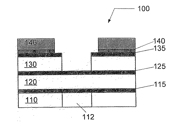
参照番号がいくつかの図の全体にわたって同一であるか対応する一部を示すように表示されている図面をここで参照して、図1Aから図1Hは、1つの実施形態に係る膜スタックの配線構造を形成する方法の概略表現を示す。方法は、第1のデュアルダマシン構造を介して複数のハードマスクにアモルファスカーボン層の集積化として特徴づけられることができる。ここに使用される用語「ビアファースト(via―first)」は、トレンチのような別の形態の形成に対するエッチングの前にビアの形成に対するエッチングがなされるプロセスを示す。 Reference is now made to the drawings wherein reference numerals are shown to indicate the same or corresponding parts throughout the several views, and FIGS. 1A through 1H illustrate a membrane stack according to one embodiment. 1 shows a schematic representation of a method for forming a wiring structure. The method can be characterized as the integration of an amorphous carbon layer on multiple hard masks via a first dual damascene structure. As used herein, the term “via-first” refers to a process in which an etch for the formation of a via is made before an etch for the formation of another form, such as a trench.
図1Aに示すように、方法は、形成された金属ライン112を有する基板110と、基板110上に形成された金属キャップ層115と、金属キャップ層115上に形成された第1の誘電体層120と、第1の誘電体層120上に形成されたエッチストップ層125と、エッチストップ層125上に形成された第2の誘電体層130と、第2の誘電体層130上に形成されたハードマスク層135と、ハードマスク層135上に形成されたアモルファスカーボン層140と、アモルファスカーボン層140上に形成された感光材料145の層とを有する膜スタック100を準備することで始まる。
As shown in FIG. 1A, the method includes a
アモルファスカーボン層と、被処理膜との間に配置されるハードマスク層135は、上部ハードマスクとしてのアモルファスカーボン層140を伴って使用される下部ハードマスクを提供することができる。これは、例えば、被処理膜にディープエッチに伴うより多くのマスク消費のために必要とされるより厚いマスクを提供する。アモルファスカーボン層が犠牲層として使われるとき、アモルファスカーボン層と、被処理膜との間に配置されるハードマスク層135は、また、デュアルダマシン構造のCMPストップ層を提供することができる。このようなCMPプロセスは、特に、銅のメタライゼーションがダマシン構造に埋められた後に磨かれるデュアルダマシンプロセスで有効である。加えて、例えば、ハードマスク層135は、より高いエッチング選択比(被処理材料と、ハードマスク材料との間の)を有するエッチングプロセスの使用を容易にすることができる。そして、このことにより、ファセット形成を低下させることによって限界寸法(CD)を維持する。
The
膜スタック100の感光材料145と接触する層としてのTERAコーティング140の利用は、配線構造の限界寸法(CD)の制御、または配線構造内のCD変化(variation)(例えば、光感応層145の層のラインエッジ粗さのための)の制御の容易にすることができる。膜スタック100の形成は、ステップを含むことができ、層間(inter−level)に対する例えば(絶縁)膜スタック、および内層間(intra−level)、シングルダマシンおよびデュアルダマシン構造のような(金属)配線構造を準備する当業者にとって知られている技術を利用することができる。
The use of the TERA coating 140 as a layer in contact with the
例えば、金属ライン112は、タングステン、アルミニウムまたは銅を含むことができる。加えて、例えば、金属キャップ層115は、窒化シリコン(Si3N4)、または(SiC)炭化珪素、またはシリコン炭窒化物(SiCN)、またはシリコン酸炭窒化物(SiCON)、またはそれらの組合せのような窒化物または炭化物材料を、または金属拡散バリアとして適切な他の膜を含むことができる。この層は、化学気相成長(CVD)またはプラズマ増強CVD(PECVD)を含むが、これに限られない方法を用いて、形成されてもよい。加えて、例えば、オプションの層であり得るエッチストップ層125(後述される)は、窒化シリコン(Si3N4)のような窒化物材料、または炭化珪素(SiC)またはシリコン酸炭化物(SiCO)のような炭化物材料、または二酸化珪素(SiO2)のような酸化物材料、またはそれらの組合せを含むことができる。この層は、化学気相成長(CVD)またはプラズマ増強CVD(PECVD)を含むが、これに限られない方法を用いて、形成されてもよい。
For example, the
第1の誘電体層120および第2の誘電体層130は、同じ材料組成または異材質組成を含むことができる。各々の誘電体層は、例えば、二酸化珪素、またはほぼ4(例えば、サーマル二酸化珪素に対する誘電率は、3.8から3.9の範囲であり得る)のSiO2の誘電率未満の公称誘電率(nominal dielectric)値を有する誘電材料を含むことができる。より詳しくは、第1および第2の誘電体層120,130は、3.7未満の誘電率、または1.6から3.7までの範囲である誘電率を有することができる。
The
各々の誘電体層120,130は、化学気相成長(CVD)またはプラズマ増強化学気相成長(PECVD)技術、または、東京エレクトロン株式会社(TEL)から市販されているClean Track ACT8 SODおよびACT12 SODコーティングシステム内でそれら誘電体層が提供されるようなスピンオン法誘電体(SOD)技術を使用して形成されることができる。Clean Track ACT8(200mm)、およびACT12(300mm)コーティングシステムは、SOD材料に対しコーティング、ベーキング、および硬化(cure)ツールを提供する。トラックシステムは、100mm、200mm、300mm、より大きい基板サイズを処理するために構成されることができる。誘電体膜を基板の上に形成する他のシステムおよび方法は、スピンオン法誘電体技術、および、CVD誘電体技術の当業者にとって周知である。
Each
さらにまた、第1および第2の誘電体層120,130は、例えば、低い誘電率(またはlow−k)の誘電体膜として、特徴づけられることになる。これらの誘電体層は、有機、無機、および無機−有機ハイブリッド材料の少なくとも1つを含むことができる。加えて、これらの誘電体層は、ポーラスであることができ、または無孔(non−porus)であることができる。例えば、これらの誘電体層は、無機、CVD技術を使用して堆積されたカーボンドーピングした酸化シリコン(または有機金属シロキサン)のようなケイ酸塩ベースの材料を含むことにできる。このような膜の実施例は、アプライドマテリアルズ株式会社から市販されているブラックダイアモンド(登録商標)CVD有機珪酸塩ガラス(organosilicate glass:OSG)膜、またはノベラスシステムから市販されているコーラル(登録商標)CVD膜を含む。別の形態として、これらの誘電体層は、硬化または小さい空所(voids)または孔(pores))を生成する堆積プロセスの間、膜の完全な焼きしまり(densification)を防止するCH3結合を有する酸化シリコンベースのマトリックスのような単一の相(single−phase)から成るポーラス無機−有機ハイブリッド膜を含むことができる。なおあるいは、これらの誘電体層は、硬化プロセスの間、分解されかつ蒸発された有機材料の孔(例えばポロゲン(porogen))を有するカーボンドープ酸化シリコンベースのマトリックスのような少なくとも2つの相から成るポーラス無機−有機ハイブリッド膜を含むことができる。なおあるいは、これらの誘電体層は、無機の、SOD技術を使用して堆積された水素シルセスキオキサン(HSQ)またはメチルシルセスキオキサン(MSQ)のようなケイ酸塩ベースの材料を含むことができる。このような膜の実施例は、ダウコーニングから市販されているFOx HSQ、ダウコーニングから市販されているXLKポーラスHSQ、およびJSRマイクロエレクトロニクスから市販されているJSR LKD−5109を含む。このような膜の実施例は、ダウケミカルから市販されているSiLK―I、SiLK−J、SiLK−H、SiLK−D、およびポーラスSiLK半導体誘電体樹脂と、ハネウェルから市販されているGX−3(登録商標)およびGX−3P(登録商標)半導体誘電体樹脂を含む。
Furthermore, the first and second
加えて、例えば、ハードマスク層135は、窒化シリコン(Si3N4)のような窒化物、炭化珪素(SiC)またはシリコン酸炭化物(SiCO)のような炭化物、または高融点金属またはタンタル窒化物(TaN)のような高融点金属窒化物、またはそれらの組合せを有することができる。この層は、化学気相成長(CVD)方法、プラズマ増強化学気相成長(PECVD)方法、および物理的気相成長(PVD)のスパッタリング方法を含むがこれに限られない方法を用いて、形成されることができる。
In addition, for example, the
アモルファスカーボン層140は、例えば、炭化水素化合物および不活性ガスを含んでいるガス混合を熱的に分解することによって形成されることができる。オプションとして添加ガスを含みうるガス混合は、処理チャンバに導入され、プラズマが基板表面付近に近づいた炭化水素化合物の熱分解を促進し、基板表面上にアモルファスカーボン層140の堆積がされる。本発明のプロセスに係る堆積されるアモルファスカーボン層140の堆積時に、約10%の水素から約60%の水素までの範囲の調整できるカーボン:水素比率を有する。アモルファスカーボン層140も、約250nm以下の波長で約0.1〜約1.0の間で変化できる減衰係数を有し、それはDUV波長での反射防止コーティング(ARC)としての使用に適している。さらに、アモルファスカーボン膜140は、ほぼ、1.50<n<1.90の屈折率の光学的範囲を示すように作成されることができる。追加の詳細は、Applied Materials社が受けた「アモルファスカーボン層を堆積させることのための方法」というタイトルの米国特許番号6,573、030号において提供される。それらの全体は、全体としてここに取り入れられる。アモルファスカーボン140の屈折率のような光学的性質は、上方の層または多層と同様に、下地の単層または多層の光学的性質に実質的に整合する(match)ように選ばれることができる。例えば、非多孔質誘電体膜のような下地層は、1.5<n<1.9の範囲の屈折率を達成することを必要とすることができ、および、ポーラス誘電体膜のような下地層は、1.2<n<2.6の範囲の屈折率を達成することを必要とすることができる。
The
加えて、例えば、感光材料145の層は、フォトレジストを含むことができ、そこにおいて、パターンは、マイクロリソグラフィを使用し、続いて光感応材料の照射を受けた領域(ポジ型フォトレジストの場合)または非照射領域(ネガ型レジストの場合)を現像溶媒を使用して除去することによって形成されることができる。例えば、感光材料145の単層(または多層)は、トラックシステムを使用して形成されることができる。トラックシステムは、248nmレジスト、193nmレジスト、157nmレジスト、EUVレジスト、(上部/下部)反射防止コーティング(TARC/BARC)、およびトップコートを処理するために構成されることができる。例えば、トラックシステムは、東京エレクトロン株式会社(TEL)から市販されているClean Track ACT8またはACT12のレジストコーティングおよび現像システムを含むことができる。フォトレジスト膜を基板上に形成する他のシステムと方法は、スピンオン法レジスト技術の当業者にとって周知である。加えて、例えば、マスクパターンは、なんらかの適切な従来のステッピングリソグラフィシステムまたはスキャンニングリソグラフィシステムを使用して形成されることができる。
In addition, for example, the layer of
一旦光感応材料145の層が膜スタック100の上に形成され、それは、上記マイクロリソグラフィ使用して第1のパターニング180でパターニングされることができる。第1のパターン180は、例えば、ビアまたはコンタクトのパターンを含むことができる。図1Bに示すように、第1のパターン180は、例えば、ドライプラズマエッチングを使用してデュアルハードマスクのアモルファスカーボン層へ転写されることができる。ドライプラズマエッチングプロセスは、酸素、弗素、塩素、臭素、水素、およびそれらの組合せからなる群から選択される少なくとも1つの種を含んでいるプラズマ化学を含むことができる。別の形態として、プラズマ化学は、窒素または希ガスのような不活性ガス(すなわちヘリウム、ネオン、アルゴン、キセノン、クリプトン、ラドン)を更に含むことができる。なお代わりとしてプラズマ化学は、アモルファスカーボン層のエッチング速度と、感光材料の上のパターン層のエッチング速度との間の高いエッチング選択比を示すために選ばれる。なお代わりとしてプラズマ化学は、アモルファスカーボン層のエッチング速度と、下層のハードマスク層のエッチング速度との間の高いエッチング選択比を示すために選ばれる。一旦第1のパターン180がアモルファスカーボン層140に転写されたならば、下層の膜スタックにエッチングするために、ハードマスクストップ層135とともに利用されるとき、パターン化されたアモルファスカーボン層140は、上部ハードマスクとして利用されることができる。残っている感光材料145は、それで、当業者にとって知られているプラズマまたは他の化学的技術を使用して取り除かれる。
Once a layer of
ここで図1Cを参照して、感光材料146の別の層は、上で記載されている技術を使用して膜スタック100の上に形成される。その中で、第2のパターン190は、マイクロリソグラフィを使用して形成される。第2のパターン190は、例えば、トレンチパターンを含むことができる。一旦第2のパターン190が感光材料146の層に形成されるならば、第2のパターン190は、アモルファスカーボン層140に転写され、図1Dに示すように、第1のパターン180は、ハードマスク層135に転写される。例えば、第2のパターンおよび第1のパターンの、アモルファスカーボン層およびハードマスク層に対するそれぞれの転写は、同時に実行されることができる。
Referring now to FIG. 1C, another layer of
アモルファスカーボン層140およびハードマスク層135にパターン転写に続いて、図1Eは、第2の誘電体層130への第1のパターン180の転写を示す。図1Eの中間のビアエッチングステップがエッチストップ層125で止められるので、図1Eの構造は、部分的なビア構造を示す。第2の誘電体層130への第1のパターン180の転写は、ドライプラズマエッチングを含むことができ、そこにおいて、プロセスは、下層のエッチストップ層125上のストップするように設定されている。
Following pattern transfer to the
例えば、酸化シリコン、二酸化珪素などのような酸化物誘電体膜をエッチングするときに、あるいは、カーボンドープされた酸化シリコン材料のような無機low−k誘電体膜をエッチングするときに、エッチング気体組成は、一般に、C4F8、C5F8、C3F6、C4F6、CF4の少なくとも1つのようなフルオロカーボンベースの化学と、不活性ガス、酸素またはCOの少なくとも1つとを含む。加えて、例えば、有機low−k誘電体膜をエッチングするときに、エッチング気体組成は、フルオロカーボンガス、窒素含有ガス、水素含有ガス、または酸素含有ガスのうちの少なくとも1つを含むことができる。選択的に誘電体膜をエッチングする技術(例えば前に記載されているような)は、誘電体のエッチングプロセスの当業者にとって周知である。プラズマ化学は、エッチストップ層125に対する第2の誘電体層130のエッチングの高選択性を呈するように選ばれることができる。エッチングプロセスは、形状および限界寸法(CD)制御、エッチング均一性(基板全体の)、マイクロトレンチングを防ぐために平坦なエッチングフロント、感光材料の層に対するエッチング選択比、および、CMPストップ層、および、エッチストップ層に対するエッチング選択比のどれか一つを呈するように選ばれることができる。
For example, when etching an oxide dielectric film such as silicon oxide, silicon dioxide, or when etching an inorganic low-k dielectric film such as a carbon-doped silicon oxide material, the etching gas composition generally, the C 4 F 8, C 5 F 8, C 3 F 6, C 4 F 6, at least one such fluorocarbon based CF 4 chemistry, inert gas, at least one of oxygen or CO Including. In addition, for example, when etching an organic low-k dielectric film, the etch gas composition can include at least one of a fluorocarbon gas, a nitrogen-containing gas, a hydrogen-containing gas, or an oxygen-containing gas. Techniques for selectively etching a dielectric film (eg, as described above) are well known to those skilled in the art of dielectric etching processes. The plasma chemistry can be chosen to exhibit a high selectivity of etching of the
ここで図1Fを参照して、第1のパターン180は、エッチストップ層125に転写され、第2のパターン190は、ハードマスク層135に転写される。例えば、第1のパターンおよび第2のパターンのエッチストップ層およびハードマスク層に対するそれぞれの転写は、同時に実行されることができる。パターン転写は、ドライプラズマエッチングを利用することができ、そこにおいて、プラズマ化学は、NF3、SF6、HBr、フルオロカーボンガス、ハイドロフルオロカーボンガス、または酸素含有ガスのうちの少なくとも1つを含んでいる。エッチングプロセスは、形状および限界寸法(CD)制御、感光材料の層に対するエッチング選択比、エッチング均一性(基板全体)、および、完全なハードマスク層の層およびエッチストップ層の除去のどれか1つでも呈するように選ばれることができる。
Referring now to FIG. 1F, the
図1Gにおいて、第2のパターン190は、第2の誘電体層130に転写され、第1のパターン180は、第1の誘電体層120に転写される。例えば、第2のパターンおよび第1のパターンの第2の誘電体層および第1の誘電体層に対する、それぞれの転写は、同時に実行されることができ、そこにおいて、第2の誘電体層に対するエッチングプロセスは、エッチストップ層125で止まり、第1の誘電体層に対するエッチングプロセスは、金属キャップ層115で止まる。エッチングプロセスは、誘電体層に対して上記されたようなプラズマ化学を利用するドライプラズマエッチングを含むことができる。エッチングプロセスは、形状および限界寸法(CD)制御、エッチング均一性(基板全体)、マイクロトレンチングを防ぐ平坦なエッチングフロント、および第1のパターン/第2のパターンコーナー選択性のどれか1つでも呈するように選ばれることができる。なんらかの残っている感光材料146でも、当業者にとって知られているプラズマまたは他の化学的技術を使用して取り除かれることができる。
In FIG. 1G, the
その後、図1Hに示すように、第1のパターン180は、例えば、ビア構造155およびトレンチ構造150の形成を完了し、金属キャップ層115に転写される。1つの実施形態において、ビア構造155およびトレンチ構造150は、同時に金属(例えば銅)で埋められる。本実施例において、アモルファスカーボン層140は、犠牲層として役立つことができ、ハードマスク層135は、銅を平坦化するCMPプロセスのCMPストップ層として役立つことができる。
Thereafter, as shown in FIG. 1H, the
別の実施形態に係る図2A〜図2Fは、膜スタック200の配線構造を形成する方法の概略表現を示す。方法は、全ビアファースト(full via first)デュアルダマシン構造内にアモルファスカーボン層の集積化として特徴づけられることができる。ここで使用しているように、「全ビアファースト」用語は、ビアの完全な形成に対するエッチングが、別の形態(例えばトレンチ)の形成に対するエッチングの前になされるプロセスを言うものである。膜スタック200は、形成された金属ライン212を有する基板210と、基板210上に形成された金属キャップ層215と、金属キャップ層215上に形成された第1の誘電体層220と、第1の誘電体層220上に形成されたエッチストップ層225と、エッチストップ層225上に形成された第2の誘電体層230と、第2の誘電体層230上に形成されたハードマスク層235と、ハードマスク層235上に形成されたアモルファスカーボン層240と、アモルファスカーボン層240上に形成された感光材料245の層とを具備し、それは、図1Aに記載された膜スタック100とほぼ同じ方法で準備されることができる。第2の誘電体層230と、アモルファスカーボン層240との間に配置されるハードマスク層235は、デュアルハードマスクと、CMPストップ層の下部層とのうちの少なくとも1つを提供することができる。アモルファスカーボン層240は、上部ハードマスクと、調整可能なARC層と、CMPストップ層と、ハードマスク層235がデュアルダマシン構造のCMPストップ層として利用されるときの犠牲層とのうちの少なくとも1つを提供することができる。
2A-2F according to another embodiment show a schematic representation of a method for forming a wiring structure of a
一旦、感光材料245の層が膜スタック200の上に形成されるならば、上記の通り、それは、マイクロリソグラフィを使用して第1のパターン280でパターニングされることができる。第1のパターン280は、例えば、ビアまたはコンタクトのパターンを含むことができる。図2Bに示すように、第1のパターン280は、アモルファスカーボン層240、ハードマスク層235、第二誘電体層230、エッチストップ層225、および第1の誘電体層220へ、例えば、ドライプラズマエッチングを使用して転写されることができる。各々の層のエッチングプロセスは、ステップを含むことができ、化学は、上記に記載したのと同様である。図2Bの中間のビアエッチングステップが金属キャップ層215で止められるので、図2Bの構造は、全ビア構造と称される。なんらか残っている感光材料245でも、それで、当業者にとって知られているプラズマまたは他の化学的技術を使用して取り除かれる。
Once a layer of
ここで図2Cを参照して、感光材料246の別の層は、上で記載されている技術を使用して膜スタック200上に形成される。その中で、第2のパターン290は、マイクロリソグラフィを使用して形成される。第2のパターン290は、例えば、トレンチパターンを含むことができる。一旦第2のパターン290が感光材料246の層に形成されるならば、第2のパターン290は、アモルファスカーボン層240、ハードマスク層235、および第2の誘電体層230に転写される。なんらかの残っている感光材料246でも、それで、当業者にとって知られているプラズマまたは他の化学的技術を使用して取り除かれる。
Referring now to FIG. 2C, another layer of
その後、図2Dに示すように、第1のパターン280は、例えば、ビア構造250およびトレンチ構造255の形成を完了して、それで、金属キャップ層215に転写される。
Thereafter, as shown in FIG. 2D, the
第1のパターン280のパターン転写に続いて光感応層245の除去の間、アッシング(またはストリッピング)プロセスがアモルファスカーボン層240の特性に影響を及ぼし得る。従って、本発明の1つの実施形態で、アモルファスカーボン層240は、取り除かれることができ、図2Eに示すように、再堆積されることができる。本実施例において、ハードマスク235は、誘電体層230へのダメージを防ぐためのエッチストップ層またはCMPストップ層として役立つことができる。その後、第2のパターン290のパターン転写は、2C図および2Dに示すように実行されることができる。しかしながら、このエッチングプロセスの間、アモルファスカーボン層240は、第1の誘電体膜220の曝露された側壁から、完全に取り除かれることができるかまたは取り除かれることができない。従って、代わりの実施形態で、図2Fに示すように、アモルファスカーボン層240は、第1のパターン転写に続いて取り除かれ、BARC層材料270は、例えば、スピンコート技術を使用して塗布される。ビア構造250を埋めているBARC層材料270は、それでドライプラズマエッチングを使用して部分的に取り除かれることができるかまたはへこませることができる。エッチング気体組成は、フルオロカーボンガス、窒素含有ガス、水素含有ガスまたは酸素含有ガスのうちの少なくとも1つを含むことができる。その後、第2のパターン290のパターン転写は、トレンチ構造255を形成する当業者にとって知られている標準の技術を使用して実行され得る。1つの実施形態において、ビア構造250およびトレンチ構造255は、同時に金属(例えば銅)で埋められる。本実施例において、アモルファスカーボン層240は犠牲層として役立つことができ、ハードマスク層235は、銅を平坦化するCMPプロセスのCMPストップ層として役立つことができる。
During the removal of the
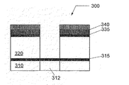
別の実施形態に係る図3A〜図3Fは、膜スタック300の配線構造を形成する方法の概略表現を示す。方法は、にストップ層のない全ビアファーストデュアルダマシン構造にアモルファスカーボン層の集積化として特徴づけられることができる。膜スタック300は、形成された金属ライン312を有する基板310と、基板310上に形成された金属キャップ層315と、金属キャップ層315上に形成された誘電体層320と、誘電体層320上に形成されたハードマスク層335と、ハードマスク層335条に形成されたアモルファスカーボン層340と、アモルファスカーボン層340上に形成された感光材料345の層とを具備し、それは、図1Aに記載された膜スタック100と、膜スタック300の各々の層はほぼ同じ方法で準備されることができる。ここで、アモルファスカーボン層340が犠牲層として使われるとき、ハードマスク層335は、デュアルハードマスク構造またはCMPストップ層の下層を提供することができる。アモルファスカーボン層340は、CMPストップ層および調整可能なARC層を提供することができる。
3A-3F according to another embodiment show a schematic representation of a method of forming a wiring structure of a
一旦感光材料345の層が膜スタック300上に形成されるならば、上記の通り、それは、マイクロリソグラフィを使用して第1のパターン380でパターニングされることができる。第1のパターン380は、例えば、ビアまたはコンタクトのパターンを含むことができる。図3Bに示すように、第1のパターン380は、例えば、ドライプラズマエッチングを使用して、アモルファスカーボン層340、ハードマスク層335,および誘電体層320へ転写されることができる。各々の層のエッチングプロセスは、ステップを含むことができ、化学は上記に記載されたのと同様である。なんらかの残っている感光材料345でも、それで、当業者にとって知られているプラズマまたは他の化学的技術を使用して取り除かれる。
Once a layer of photosensitive material 345 is formed on the
ここで図3Cを参照して、感光材料346の別の層は、上で記載されている技術を使用して膜スタック300上に形成される。その中で、第2のパターン390は、マイクロリソグラフィを使用して形成される。第2のパターン390は、例えば、トレンチパターンを含むことができる。一旦第2のパターン390が感光材料346の層に形成されるならば、第2のパターン390は、アモルファスカーボン層340、ハードマスク層335,および誘電体層320の上部へ転写される。第2のパターン390が誘電体層320に転写される深さは、エッチングプロセス中のエッチング時間を増加または減少させることによって調整されることができる。なんらかの残っている感光材料346でも、それで、当業者にとって知られているプラズマまたは他の化学的技術を使用して取り除かれる。その後、図3Dに示すように、第1のパターン380は、例えば、ビア構造350およびトレンチ構造355の形成を完了して、それで金属キャップ層315に転写される。1つの実施形態において、ビア構造350およびトレンチ構造255は、同時に金属(例えば銅)で埋められる。本実施例において、アモルファスカーボン層340は、犠牲層として役立つことができ、ハードマスク層335は、銅を平坦化するCMPプロセスのCMPストップ層として役立つことができる。
Referring now to FIG. 3C, another layer of
上述の通り、第1のパターン380のパターン転写に続いて光感応層345の除去の間、アッシング(またはストリッピング)プロセスがアモルファスカーボン層340の特性に影響を及ぼし得る。従って、実施例において、アモルファスカーボン層340は、取り除かれることができ、図3Eに示すように再堆積されることができる。本実施例において、ハードマスク335は、誘電体層320へのダメージを防ぐためのエッチストップ層またはCMPストップ層として役立つことができる。その後、第2のパターン390のパターン転写は、図3Cおよび3Dに示すように実行されることができる。しかしながら、このエッチングプロセスの間、アモルファスカーボン層340は、誘電体層320の曝露された側壁から、完全に取り除かれることができるかまたは取り除かれることができない。代わりの実施形態では、図3Fに示すように、アモルファスカーボン層340は第1のパターン転写に引き続いて取り除かれ、BARC層370は、例えば、スピンコート技術を使用して塗布される。ビア構造350を埋めているBARC層材料370は、ドライプラズマエッチングを使用して、それで部分的に取り除かれることができるかまたはへこまされることができる。エッチング気体組成は、フルオロカーボンガス、窒素含有ガス、水素含有ガス、または酸素含有ガスのうちの少なくとも1つを含むことができる。その後、第2のパターン390のパターン転写は、当業者にとって知られている標準の技術を使用して実行され得る。
As described above, during the removal of the photosensitive layer 345 following the pattern transfer of the
さらにもう一つの実施形態に係る、図4A〜図4Kは、膜スタック400の配線構造を形成する方法の概略表現を示す。方法は、複数のハードマスクトレンチファーストデュアルダマシン構造にアモルファスカーボン層の集積化として特徴づけられることができる。膜スタック400は、形成された金属ライン412を有する基板410と、基板410上に形成された金属キャップ層415と、金属キャップ層415上に形成された第1の誘電体層420と、第1の誘電体層420上に形成された(オプションの)エッチストップ層425と、(オプションの)エッチストップ層425上に形成された第2の誘電体層430と、第2の誘電体層430上に形成された(オプションの)ハードマスク層435と、ハードマスク層435上に形成された第1のアモルファスカーボン層440と、第1のアモルファスカーボン層440上に形成された第2のアモルファスカーボン層441と、アモルファスカーボン層441上に形成された感光材料445の層とを具備し、それは、図1Aに記載された膜スタック100と、ほぼ同じ方法で準備されることができる。ハードマスク層435は、デュアルハードマスク構造の下部層およびCMPストップ層のうちの少なくとも一方を提供することができる。第2のアモルファスカーボン層441は、上部ハードマスクと、調整可能なARC層と、CMPストップ層と、ハードマスク層435がデュアルダマシン構造のCMPストップ層として利用されるときの犠牲層とのうちの少なくとも1つを提供することができる。
4A-4K, according to yet another embodiment, show a schematic representation of a method for forming a wiring structure of a
一旦感光材料445の層が膜スタック400の上に形成されるならば、上記の通り、それは、マイクロリソグラフィを使用して第1のパターン480でパターニングされることができる。第1のパターン480は、例えば、トレンチのパターンを含むことができる。図4Bに示すように、第1のパターン480は、例えば、ドライプラズマエッチングを使用して第2のアモルファスカーボン層441へ転写されることができる。エッチングプロセスは、ステップを含むことができ、化学は、上記に記載したのと同様である。なんらかの残っている感光材料445でも、当業者にとって知られているプラズマまたは他の化学的技術を使用して取り除かれることができる。
Once a layer of
ここで図4Cを参照して、感光材料446の別の層は、上で記載されている技術を使用して膜スタック400上に形成される。その中で、第2のパターン490は、マイクロリソグラフィを使用して形成される。第2のパターン490は、例えば、ビアパターンを含むことができる。図4Dに示すように、一旦第2のパターン490が感光材料445の層に形成されるならば、第2のパターン490は、第1のアモルファスカーボン層440およびハードマスク層435に転写される。
Referring now to FIG. 4C, another layer of
その後、図4Eに示すように、第2のパターン490は、第2の誘電体層430に転写される。図4Fを、ここで参照する。なんらかの残っている感光材料446でも、それで、当業者にとって知られているプラズマまたは他の化学的技術を使用して取り除かれる。
Thereafter, as shown in FIG. 4E, the
図4Gにおいて、第1のパターン480は、第1のアモルファスカーボン層へ転写され、第2のパターン490は、(オプションの)エッチストップ層425に転写される。第1のパターンおよび第2のパターンの第1のアモルファスカーボン層および(オプションの)エッチストップ層に対するそれぞれの転写は、同時に実行されることができ、そこにおいて、第1のアモルファスカーボン層のエッチングプロセスは、ハードマスク層435に止まり、および、(オプションの)エッチストップ層のエッチングプロセスは、第1の誘電体層420で止まる。エッチングプロセスは、誘電体層に対する上記のようなプラズマ化学を利用するドライプラズマエッチングを含むことができる。エッチングプロセスは、形状および限界寸法(CD)制御、エッチング均一性(基板全体)、マイクロトレンチングを防ぐ平坦なエッチングフロント、および第1のパターン/第2のパターンコーナー選択性のどれか1つを呈するように選ばれることができる。
In FIG. 4G, the
ここで図4Hを参照して、第1のパターン480は、ハードマスク層435に転写され、第2のパターン490は、第一誘電体層420に部分的に転写される。その後、図41に示すように、第1のパターン480は、第2の誘電体層430に転写され、第2のパターン490は、第1の誘電体層420に転写される。第1のパターンおよび第2のパターンの第2の誘電体層および第1の誘電体層に対するそれぞれの転写は、同時に実行されることができ、そこにおいて、第2の誘電体層のエッチングプロセスは、エッチストップ層425で止まり、第1の誘電体層のエッチングプロセスは、金属キャップ層415で止まる。エッチングプロセスは、誘電体層に対して上記のようなプラズマ化学を利用するドライプラズマエッチングを含むことができる。エッチングプロセスは、形状および限界寸法(CD)制御、エッチング均一性(基板全体に)、マイクロトレンチングを防ぐ平坦なエッチングフロント、および第1のパターン/第2のパターンコーナー選択性のどれか1つでも呈するように選ばれることができる。
Referring now to FIG. 4H, the
その後、図4Jに示すように、第2のパターン490は、例えば、ビア構造455およびトレンチ構造450の形成を完了して、それで金属キャップ層415に転写される。1つの実施形態において、ビア構造455およびトレンチ構造450は、同時に金属(例えば銅)で埋められる。本実施例において、アモルファスカーボン層440は、犠牲層として役立つことができ、ハードマスク層435は、銅を平坦化するCMPプロセスのCMPストップ層として役立つことができる。
Thereafter, as shown in FIG. 4J, the
別の実施形態に係る図5A〜図5Dは、膜スタック500の配線構造を形成する方法の概略表現を示す。方法は、埋込み型ビアマスクデュアルダマシン構造でアモルファスカーボン層の集積化として特徴づけられることができる。膜スタック500は、形成された金属ライン512を有する基板510と、基板510上に形成された金属キャップ層515と、金属キャップ層515上に形成された第1の誘電体層520と、第1の誘電体層520上に形成された第1のアモルファスカーボン層540と、第1のアモルファスカーボン層540上に形成された感光材料545の層とを具備する。各々の層は、図1Aに記載された膜スタック100とほぼ同じ方法で準備されることができる。
5A-5D according to another embodiment show a schematic representation of a method of forming a wiring structure of a
一旦光感応材料545の層が膜スタック500の上に形成されると、それは、上記の通り、マイクロリソグラフィを使用して第1のパターニング580でパターニングされることができる。第1のパターン580は、例えば、ビアまたはコンタクトのパターンを含むことができる。図5Bに示すように、第1のパターン580は、例えば、ドライプラズマエッチングを使用して、第1のアモルファスカーボン層540へ転写されることができる。第1のアモルファスカーボン層のエッチングプロセスは、ステップを含むことができ、化学は、上記に記載したものと同様である。エッチングプロセスに続き、感光材料545の残っている層は、当業者にとって知られているプラズマまたは他の化学的技術を使用して取り除かれる。
Once a layer of
ここで図5Cを参照して、第2の誘電体層530は、パターン化された第1のアモルファスカーボン層540上に形成され、ハードマスク層535は、第2の誘電体層530上に形成され、第2のアモルファスカーボン層542は、ハードマスク層535上に形成され、感光材料546の別の層は、第2のアモルファスカーボン層542上に形成される。各々の層は、図1Aに記載された膜スタック100とほぼ同じ方法で準備されることができる。ハードマスク層535は、下部ハードマスクおよびCMPストップ層のうちの少なくとも1つを提供することができ、アモルファスカーボン層540は、上部ハードマスクと、調整可能なARC層と、CMPストップ層と、ハードマスク層535がデュアルダマシン構造のCMPストップ層として利用されるときの犠牲層とのうちの少なくとも1つを提供することができる。
Referring now to FIG. 5C, a
一旦感光材料546の追加の層が膜スタック500上に形成されると、第2のパターン590は、マイクロリソグラフィを使用して形成される。第2のパターン590は、例えば、トレンチのパターンを含むことができる。図5Dに示すように、一旦第2のパターン590が感光材料546の層に形成されるならば、第2のパターン590は、例えば、ドライプラズマエッチングを使用して、第2のアモルファスカーボン層542、ハードマスク層535、および第2の誘電体層530に転写される。第1のアモルファスカーボン層540がエッチストップ層として役立つとともに、第1のパターン580は、例えば、ドライプラズマエッチングを使用して第1の誘電体層520に転写される。何らかの残っている感光材料546でも、当業者にとって知られているプラズマまたは他の化学的技術を使用して取り除かれることができる。その後、金属キャップ層515は、例えば、ビア構造550およびトレンチ構造555の形成を完了して、それで取り除かれることができる。各々の層のエッチングプロセスは、ステップを含むことができ、化学は、上記に記載したのと同様である。さらに、実施例において、ビア構造550およびトレンチ構造555は、同時に金属(例えば銅)で埋められる。本実施例において、アモルファスカーボン層542は、犠牲層として役立つことができ、ハードマスク層535は、銅を平坦化するCMPプロセスのCMPストップ層として役立つことができる。
Once an additional layer of photosensitive material 546 is formed on the
別の実施形態に係る図6A〜図6Iは、膜スタック600の配線構造を形成する方法の概略表現を示す。方法は、シングルダマシン構造でアモルファスカーボン層の集積化として特徴づけられることができる。膜スタック600は、形成された金属ライン612を有する基板610と、基板610上に形成された金属キャップ層615と、金属キャップ層615上に形成された第1の誘電体層620と、第1の誘電体層620上に形成された第1のハードマスク625と、第1のハードマスク625上に形成された第1のアモルファスカーボン層640と、第1のアモルファスカーボン層640上に形成された感光材料645の層とを具備する。各々の層は、図1Aに記載された膜スタック100とほぼ同じ方法で準備されることができる。
6A-6I according to another embodiment show a schematic representation of a method of forming a wiring structure of a
膜スタック600がハードマスク層625を包含するときに、ハードマスク層625はハードマスクまたはCMPストップ層のうちの少なくとも1つを提供することができ、第1のアモルファスカーボン層640は、上部ハードマスクと、
調整可能なARC層と、CMPストップ層とのうちの少なくとも1つを提供することができる。
When the
At least one of a tunable ARC layer and a CMP stop layer may be provided.
一旦感光材料645の層が膜スタック600上に形成されると、上記の通り、それは、マイクロリソグラフィを使用して第1のパターン680でパターニングされることができる。第1のパターン680は、例えば、ビアまたはコンタクトのパターンを含むことができる。図6Bに示すように、第1のパターン680は、例えば、ドライプラズマエッチングを使用して、第1のアモルファスカーボン層640および(オプションの)第1のハードマスク625に転写されることができる。エッチングプロセス(単一のプロセスまたは複数のプロセス)は、ステップを含むことができ、化学は、上記に記載されたのと同様である。その後、図6Cに示すように、第1のパターン680は、例えば、ドライプラズマエッチングを使用して第1の誘電体層620に転写される。エッチングプロセスは、ステップを含むことができ、化学は、上記に記載されたのと同様である。エッチングプロセスに続いて、図6Dにて図示したように、感光材料645の残っている層は、当業者にとって知られているプラズマまたは他の化学的技術を使用して取り除かれる。
Once the layer of
ここで図6Eを参照して、第1のパターン680は、例えば、ドライプラズマエッチングを使用して金属キャップ層615に転写される。エッチングプロセスは、ステップを含むことができ、化学は、上記に記載されたのと同様である。
Referring now to FIG. 6E, the
ここで図6Fを参照して、アルミニウムまたは銅のような金属は、物理気相成長法(PVD)、CVD、PECVD、電気メッキ、またはそれらのなんらかの組合せの少なくとも1つを使用して、第1の誘電体層620に第1のパターン(またはビア)を埋めるように、膜スタック600上に堆積される。一旦金属堆積が完了すると、例えば、第1のハードマスク層625に対しCMPを使用して、金属はポリッシュされる。本実施例において、アモルファスカーボン層640が犠牲層として使われ、ハードマスク625は、CMPストップ層である。その後、第2の金属キャップ層626は、第1のハードマスク層625および金属が埋め込まれた第1のパターン(またはビア)613の上に形成され、第2の誘電体層630は、第2の金属キャップ層626上に形成され、第2のハードマスク層635は、第2の誘電体層630上に形成され、第2のアモルファスカーボン層641は、第2のハードマスク層635上に形成され、および、光感応材料646の別の層は、第2のアモルファスカーボン層641上に形成される。各々の層は、図1Aに記載された膜スタック100と、ほぼ同じ方法で準備されることができる。ハードマスク層635は、ハードマスクまたはCMPストップ層のうちの少なくとも1つを提供することができ、第2のアモルファスカーボン層641は、上部ハードマスクと、調整可能なARC層と、CMPストップ層とのうちの少なくとも1つを提供することができる。
Referring now to FIG. 6F, a metal, such as aluminum or copper, can be formed using at least one of physical vapor deposition (PVD), CVD, PECVD, electroplating, or some combination thereof. The
一旦感光材料646の追加の層が膜スタック600上に形成されると、第2のパターン690は、マイクロリソグラフィを使用して形成される。第2のパターン690は、例えば、トレンチのパターンを含むことができる。図6Gに示すように、一旦第2のパターン690が感光材料646の層に形成されるならば、第2のパターン690は、例えば、ドライプラズマエッチングを使用して、第2のアモルファスカーボン層641、第2のハードマスク層635、および第2の誘電体層630に転写される。図6Hにて図示したように、なんらかの残っている感光材料646でも、当業者にとって知られているプラズマまたは他の化学的技術を使用して取り除かれることができる。その後、第2の金属キャップ層626は、例えば、ビア構造650(金属で埋められる)およびトレンチ構造655(金属埋め込みのために準備される)の形成を完了して、それで、取り除かれることができる。各々の層のエッチングプロセスは、ステップを含むことができ、化学は、上記に記載されたのと同様である。1つの実施形態において、トレンチ構造655は、金属(例えば銅)で埋められる。本実施例において、アモルファスカーボン層641は、銅を平坦化するCMPプロセスの犠牲層として役立つことができる。
Once an additional layer of
本発明の特定の典型的な実施形態だけが上で詳述されており、当業者は、多くの変更態様が本発明の新規進歩の事項から逸脱することなく例示的実施態様で可能であると容易に理解する。したがって、全てのこのような変更態様は、本発明の範囲内に包含されることを目的とするものである。 Only certain exemplary embodiments of the present invention have been described in detail above, and those skilled in the art will recognize that many variations are possible in the exemplary embodiments without departing from the novel advances of the invention. Easy to understand. Accordingly, all such modifications are intended to be included within the scope of this invention.
Claims (36)
この半導体基板の上に形成され、被処理膜を含む膜スタックと、
アモルファスカーボン層、およびアモルファスカーボン層と被処理膜との間に配置される下層のアモルファスカーボン層を含まないハードマスク層を含むデュアルハードマスクと、
膜スタックに形成された金属配線のためのダマシン構造とを具備する半導体デバイス。 A semiconductor substrate;
A film stack formed on the semiconductor substrate and including a film to be processed;
A dual hard mask including an amorphous carbon layer, and a hard mask layer not including an amorphous carbon layer as a lower layer disposed between the amorphous carbon layer and the film to be processed;
A damascene structure for metal wiring formed in a film stack.
ハードマスク層を前記誘電体材料層の上に形成することと、
アモルファスカーボン材料の層を前記ハードマスク層の上に形成することと、
配線構造の形成のためのリソグラフィ構造として、デュアルハードマスクの上部層として、反射防止コーティングとして、およびケミカルメカニカルポリシング(CMP)プロセスの犠牲層としての前記アモルファスカーボン材料の層を用いて金属配線のためのダマシン構造を形成することと、を具備し、
前記ハードマスク層は、CMPストップ層として用いられる集積回路構造を形成するためのプロセス。 Forming a dielectric material layer on the substrate;
Forming a hard mask layer on the dielectric material layer;
Forming a layer of amorphous carbon material on the hard mask layer;
For metal wiring using the layer of amorphous carbon material as a lithographic structure for the formation of a wiring structure, as an upper layer of a dual hard mask, as an anti-reflective coating, and as a sacrificial layer in a chemical mechanical polishing (CMP) process Forming a damascene structure of
The hard mask layer is a process for forming an integrated circuit structure used as a CMP stop layer.
放射線のパターンに前記感光材料の層を露光させることとを更に具備し、
前記アモルファスカーボン材料の層を前記形成することは、前記放射線のパターンと実質的に同様の前記感光材料の層にパターンを作成するのを容易にする請求項20のプロセス。 Forming a layer of a photosensitive material having optical properties substantially the same as the optical properties of the amorphous carbon material layer on the amorphous carbon material layer;
Further exposing the layer of photosensitive material to a pattern of radiation,
21. The process of claim 20, wherein said forming said layer of amorphous carbon material facilitates patterning said layer of photosensitive material substantially similar to said radiation pattern.
基板上に形成された金属キャップ層と、
前記金属キャップ層上に形成された第1の誘電体層と、
前記第1の誘電体層上に形成された第2の誘電体層と、
前記第2の誘電体層上に形成されたハードマスク層と、
前記ハードマスク層上に形成された第1のアモルファスカーボン層と、
前記第1のアモルファスカーボン層上に形成された第2のアモルファスカーボン層と、前記第2のアモルファスカーボン層上に形成された光感応材料の第1の層と、を有する、前記基板を含む膜スタックを準備することと;
前記感光材料の第1の層に第1のパターンを形成することと;
前記第1のパターンを前記第2のアモルファスカーボン層に転写することと;
感光材料の第2の層を前記第2のアモルファスカーボン層上に形成することと;
前記感光材料の第2の層に第2のパターンを形成することと;
前記第2のパターンを前記第1のアモルファスカーボン層に転写すること;
前記第2のパターンを前記ハードマスク層に転写することと;
前記第2のパターンを前記第2の誘電体層に転写すること;
前記第2のパターンを前記第1の誘電体層に転写すること;
前記第1のパターンを前記第1のアモルファスカーボン層に転写すること;
前記第1のパターンを前記ハードマスク層に転写すること;
前記第1のパターンを前記第2の誘電体層に転写することと、
前記第2のパターンを前記金属キャップ層に転写することと、を具備する配線構造を形成する方法。 Metal lines,
A metal cap layer formed on the substrate;
A first dielectric layer formed on the metal cap layer;
A second dielectric layer formed on the first dielectric layer;
A hard mask layer formed on the second dielectric layer;
A first amorphous carbon layer formed on the hard mask layer;
A film including the substrate, comprising: a second amorphous carbon layer formed on the first amorphous carbon layer; and a first layer of photosensitive material formed on the second amorphous carbon layer. Preparing a stack;
Forming a first pattern in the first layer of the photosensitive material;
Transferring the first pattern to the second amorphous carbon layer;
Forming a second layer of photosensitive material on the second amorphous carbon layer;
Forming a second pattern on the second layer of photosensitive material;
Transferring the second pattern to the first amorphous carbon layer;
Transferring the second pattern to the hard mask layer;
Transferring the second pattern to the second dielectric layer;
Transferring the second pattern to the first dielectric layer;
Transferring the first pattern to the first amorphous carbon layer;
Transferring the first pattern to the hard mask layer;
Transferring the first pattern to the second dielectric layer;
Transferring the second pattern to the metal cap layer, and forming a wiring structure.
前記第2のパターンを前記エッチストップ層に転写することとを更に具備する請求項27または28の方法。 Providing the film stack with an etch stop layer formed on the first dielectric layer before the second dielectric layer formed on the etch stop layer;
29. The method of claim 27 or 28, further comprising transferring the second pattern to the etch stop layer.
犠牲層として前記アモルファスカーボン層の少なくとも1つを使用して、およびストップ層として前記ハードマスク層を使用して金属をケミカルメカニカルポリシングすることとを更に具備する請求項27の方法。 Filling the first and second patterns with metal;
28. The method of claim 27, further comprising: chemical mechanical polishing the metal using at least one of the amorphous carbon layer as a sacrificial layer and using the hard mask layer as a stop layer.
前記基板の上に形成される金属キャップ層と、
前記金属キャップ層の上に形成される第1の誘電体層と、
前記第1の誘電体層の上に形成されるアモルファスカーボン層と、
前記アモルファスカーボン層の上に形成される光感応材料の第1の層と、を有する、基板を含む膜スタックを準備することと;
感光材料の前記第1の層の第1のパターンを形成することと;
前記第1のパターンを前記アモルファスカーボン層に転写することと;
第2の誘電体層を前記アモルファスカーボン層および前記第1のパターンの上に形成することと;
ハードマスクを前記第2の誘電体層の上に形成することと;
第2のアモルファスカーボン層を前記ハードマスクの上に形成することと;
感光材料の第2の層を前記第2のアモルファスカーボン層の上に形成することと;
感光材料の前記第2の層の第2のパターンを形成することと;
前記第2のパターンを前記第2のアモルファスカーボン層に転写することと;
前記ハードマスクに前記第2のパターンを転写することと;
前記第2のパターンを前記第2の誘電体層に転写することと;
前記第1のパターンを前記第一誘電体層に転写することと;
前記第1のパターンを前記金属キャップ層に転写することとを具備する配線構造を形成する方法。 Metal lines,
A metal cap layer formed on the substrate;
A first dielectric layer formed on the metal cap layer;
An amorphous carbon layer formed on the first dielectric layer;
Providing a film stack including a substrate having a first layer of photosensitive material formed on the amorphous carbon layer;
Forming a first pattern of the first layer of photosensitive material;
Transferring the first pattern to the amorphous carbon layer;
Forming a second dielectric layer on the amorphous carbon layer and the first pattern;
Forming a hard mask over the second dielectric layer;
Forming a second amorphous carbon layer on the hard mask;
Forming a second layer of photosensitive material on the second amorphous carbon layer;
Forming a second pattern of the second layer of photosensitive material;
Transferring the second pattern to the second amorphous carbon layer;
Transferring the second pattern to the hard mask;
Transferring the second pattern to the second dielectric layer;
Transferring the first pattern to the first dielectric layer;
Transferring the first pattern to the metal cap layer; and forming a wiring structure.
犠牲層として前記アモルファスカーボン層を使用していて、およびストップ層として前記ハードマスクを使用して金属をケミカルメカニカルポリシングすることとを更に具備する請求項32の方法。 Filling the first and second patterns with metal;
33. The method of claim 32, further comprising using the amorphous carbon layer as a sacrificial layer and chemically mechanically polishing the metal using the hard mask as a stop layer.
前記基板の上に形成される金属キャップ層と、
前記金属キャップ層の上に形成される第1の誘電体層と、
前記第1の誘電体層の上に形成されるハードマスクと、
前記ハードマスク層の上に形成されるアモルファスカーボン層と、
前記アモルファスカーボン層の上に形成される光感応材料の第1の層と、を有する、基板を含む膜スタックを準備することと;
第1のパターンを感光材料の前記第1の層に形成することと;
前記第1のパターンを前記アモルファスカーボン層に転写することと;
前記第1のパターンを前記ハードマスク層に転写することと;
前記第1のパターンを前記第1の誘電体層に転写することと;
前記第1のパターンを前記金属キャップ層に転写することと;
前記アモルファスカーボン層を除去することと;
前記第1の誘電体層および前記金属キャップ層の前記第1のパターンを金属で埋めることと;
第2の金属キャップ層を前記膜スタックの上に形成することと;
第2の誘電体層を前記第2の金属キャップ層の上に形成することと;
第2のハードマスク層を前記第2の誘電体層の上に形成することと;
第2のアモルファスカーボン層を前記第2のハードマスク層の上に形成することと;
感光材料の第2の層を前記第2のアモルファスカーボン層の上に形成することと;
第2のパターンを光感応材料の前記第2の層に形成することと;
前記第2のパターンを前記第2のアモルファスカーボン層に転写すること;
前記第2のパターンを前記第2のハードマスク層に転写することと;
前記第2のパターンを前記第2の誘電体層に転写することと;
前記第2のパターンを前記第2の金属キャップ層に転写することとを具備する配線構造を形成する方法。 Metal lines,
A metal cap layer formed on the substrate;
A first dielectric layer formed on the metal cap layer;
A hard mask formed on the first dielectric layer;
An amorphous carbon layer formed on the hard mask layer;
Providing a film stack including a substrate having a first layer of photosensitive material formed on the amorphous carbon layer;
Forming a first pattern in the first layer of photosensitive material;
Transferring the first pattern to the amorphous carbon layer;
Transferring the first pattern to the hard mask layer;
Transferring the first pattern to the first dielectric layer;
Transferring the first pattern to the metal cap layer;
Removing the amorphous carbon layer;
Filling the first pattern of the first dielectric layer and the metal cap layer with metal;
Forming a second metal cap layer on the membrane stack;
Forming a second dielectric layer on the second metal cap layer;
Forming a second hard mask layer on the second dielectric layer;
Forming a second amorphous carbon layer on the second hard mask layer;
Forming a second layer of photosensitive material on the second amorphous carbon layer;
Forming a second pattern in the second layer of photosensitive material;
Transferring the second pattern to the second amorphous carbon layer;
Transferring the second pattern to the second hard mask layer;
Transferring the second pattern to the second dielectric layer;
Transferring the second pattern to the second metal cap layer; and forming a wiring structure.
CMPストップ層として犠牲層および前記第2のハードマスクとして前記第2のアモルファス層を使用して金属をケミカルメカニカルポリシングすることとを更に具備する請求項34の方法。 Filling the second pattern with metal;
36. The method of claim 34, further comprising chemical mechanical polishing the metal using a sacrificial layer as a CMP stop layer and the second amorphous layer as the second hard mask.
前記第2のパターンを前記エッチストップ層に転写することとを更に具備する請求項29の方法。 Providing the film stack with an etch stop layer formed on the first dielectric layer before the second dielectric layer formed on the etch stop layer;
30. The method of claim 29, further comprising transferring the second pattern to the etch stop layer.
Applications Claiming Priority (2)
| Application Number | Priority Date | Filing Date | Title |
|---|---|---|---|
| US10/766,872 US7115993B2 (en) | 2004-01-30 | 2004-01-30 | Structure comprising amorphous carbon film and method of forming thereof |
| PCT/US2004/039771 WO2005074449A2 (en) | 2004-01-30 | 2004-12-17 | Structure comprising amorphous carbon film and method of forming thereof |
Publications (2)
| Publication Number | Publication Date |
|---|---|
| JP2007523034A true JP2007523034A (en) | 2007-08-16 |
| JP2007523034A5 JP2007523034A5 (en) | 2008-01-31 |
Family
ID=34807608
Family Applications (1)
| Application Number | Title | Priority Date | Filing Date |
|---|---|---|---|
| JP2006551053A Withdrawn JP2007523034A (en) | 2004-01-30 | 2004-12-17 | Structure including amorphous carbon film and method for forming the same. |
Country Status (4)
| Country | Link |
|---|---|
| US (1) | US7115993B2 (en) |
| JP (1) | JP2007523034A (en) |
| TW (1) | TWI280987B (en) |
| WO (1) | WO2005074449A2 (en) |
Cited By (11)
| Publication number | Priority date | Publication date | Assignee | Title |
|---|---|---|---|---|
| JP2007128938A (en) * | 2005-11-01 | 2007-05-24 | Elpida Memory Inc | Manufacturing method of semiconductor device |
| JP2009253246A (en) * | 2008-04-11 | 2009-10-29 | Spansion Llc | Semiconductor device, and manufacturing method thereof |
| JP2009253245A (en) * | 2008-04-11 | 2009-10-29 | Spansion Llc | Method for manufacturing semiconductor device |
| JP2010503218A (en) * | 2006-08-29 | 2010-01-28 | マイクロン テクノロジー, インク. | Semiconductor devices including fine pitch arrays with staggered contacts and methods for their design and manufacture |
| JP5113830B2 (en) * | 2007-02-28 | 2013-01-09 | 東京エレクトロン株式会社 | Method for forming amorphous carbon film, method for manufacturing semiconductor device, and computer-readable storage medium |
| KR20130046351A (en) | 2011-10-27 | 2013-05-07 | 도쿄엘렉트론가부시키가이샤 | Film forming apparatus and method of operating the same |
| JP2013093526A (en) * | 2011-10-27 | 2013-05-16 | Tokyo Electron Ltd | Deposition apparatus and operation method of the same |
| US8592324B2 (en) | 2010-02-05 | 2013-11-26 | Tokyo Electron Limited | Method for forming laminated structure including amorphous carbon film |
| JP2023524253A (en) * | 2020-05-05 | 2023-06-09 | ラム リサーチ コーポレーション | Inert gas injection for improved hard mask selectivity |
| KR20250022720A (en) | 2022-06-15 | 2025-02-17 | 가부시끼가이샤 레조낙 | CMP polishing solution and polishing method |
| KR102915604B1 (en) | 2020-05-05 | 2026-01-21 | 램 리써치 코포레이션 | Inert gas injection to improve hard mask selectivity |
Families Citing this family (47)
| Publication number | Priority date | Publication date | Assignee | Title |
|---|---|---|---|---|
| US7504727B2 (en) | 2004-05-14 | 2009-03-17 | International Business Machines Corporation | Semiconductor interconnect structure utilizing a porous dielectric material as an etch stop layer between adjacent non-porous dielectric materials |
| US7371461B2 (en) * | 2005-01-13 | 2008-05-13 | International Business Machines Corporation | Multilayer hardmask scheme for damage-free dual damascene processing of SiCOH dielectrics |
| US7291553B2 (en) * | 2005-03-08 | 2007-11-06 | Taiwan Semiconductor Manufacturing Co., Ltd. | Method for forming dual damascene with improved etch profiles |
| US7312162B2 (en) | 2005-05-17 | 2007-12-25 | Applied Materials, Inc. | Low temperature plasma deposition process for carbon layer deposition |
| US7422775B2 (en) | 2005-05-17 | 2008-09-09 | Applied Materials, Inc. | Process for low temperature plasma deposition of an optical absorption layer and high speed optical annealing |
| US7857982B2 (en) * | 2005-07-19 | 2010-12-28 | Micron Technology, Inc. | Methods of etching features into substrates |
| US7312148B2 (en) | 2005-08-08 | 2007-12-25 | Applied Materials, Inc. | Copper barrier reflow process employing high speed optical annealing |
| US7335611B2 (en) | 2005-08-08 | 2008-02-26 | Applied Materials, Inc. | Copper conductor annealing process employing high speed optical annealing with a low temperature-deposited optical absorber layer |
| US7429532B2 (en) | 2005-08-08 | 2008-09-30 | Applied Materials, Inc. | Semiconductor substrate process using an optically writable carbon-containing mask |
| US7323401B2 (en) * | 2005-08-08 | 2008-01-29 | Applied Materials, Inc. | Semiconductor substrate process using a low temperature deposited carbon-containing hard mask |
| US7422975B2 (en) * | 2005-08-18 | 2008-09-09 | Sony Corporation | Composite inter-level dielectric structure for an integrated circuit |
| US7602068B2 (en) | 2006-01-19 | 2009-10-13 | International Machines Corporation | Dual-damascene process to fabricate thick wire structure |
| US7563688B2 (en) * | 2006-02-24 | 2009-07-21 | Hynix Semiconductor Inc. | Method for fabricating capacitor in semiconductor device |
| US20070243714A1 (en) * | 2006-04-18 | 2007-10-18 | Applied Materials, Inc. | Method of controlling silicon-containing polymer build up during etching by using a periodic cleaning step |
| US7867578B2 (en) * | 2006-06-28 | 2011-01-11 | Applied Materials, Inc. | Method for depositing an amorphous carbon film with improved density and step coverage |
| US8129282B2 (en) * | 2006-07-19 | 2012-03-06 | Tokyo Electron Limited | Plasma etching method and computer-readable storage medium |
| JP2008028022A (en) * | 2006-07-19 | 2008-02-07 | Tokyo Electron Ltd | Plasma etching method and computer-readable storage medium |
| US20080124912A1 (en) * | 2006-08-01 | 2008-05-29 | Taiwan Semiconductor Manufacturing Co., Ltd. | Semiconductor methods |
| US7517804B2 (en) * | 2006-08-31 | 2009-04-14 | Micron Technologies, Inc. | Selective etch chemistries for forming high aspect ratio features and associated structures |
| JP4237216B2 (en) * | 2006-10-05 | 2009-03-11 | Necエレクトロニクス株式会社 | Manufacturing method of semiconductor device |
| US8426818B2 (en) * | 2007-02-05 | 2013-04-23 | Bae Systems Information And Electronic Systems Integration Inc. | Post-supported microbolometer pixel |
| US7763987B2 (en) | 2007-02-27 | 2010-07-27 | Qimonda Ag | Integrated circuit and methods of manufacturing a contact arrangement and an interconnection arrangement |
| TWI455203B (en) * | 2007-05-03 | 2014-10-01 | 蘭姆研究公司 | Hard mask of the opening and etching contour control by hard masking of the opening |
| US7858514B2 (en) | 2007-06-29 | 2010-12-28 | Qimonda Ag | Integrated circuit, intermediate structure and a method of fabricating a semiconductor structure |
| US8021933B2 (en) | 2007-08-29 | 2011-09-20 | Qimonda Ag | Integrated circuit including structures arranged at different densities and method of forming the same |
| US7709370B2 (en) * | 2007-09-20 | 2010-05-04 | International Business Machines Corporation | Spin-on antireflective coating for integration of patternable dielectric materials and interconnect structures |
| US8084862B2 (en) * | 2007-09-20 | 2011-12-27 | International Business Machines Corporation | Interconnect structures with patternable low-k dielectrics and method of fabricating same |
| US8618663B2 (en) * | 2007-09-20 | 2013-12-31 | International Business Machines Corporation | Patternable dielectric film structure with improved lithography and method of fabricating same |
| US8298931B2 (en) * | 2007-09-28 | 2012-10-30 | Sandisk 3D Llc | Dual damascene with amorphous carbon for 3D deep via/trench application |
| US9136463B2 (en) * | 2007-11-20 | 2015-09-15 | Qualcomm Incorporated | Method of forming a magnetic tunnel junction structure |
| DE102008016425B4 (en) * | 2008-03-31 | 2015-11-19 | Advanced Micro Devices, Inc. | A method of patterning a metallization layer by reducing degradation of the dielectric material caused by resist removal |
| US20090266790A1 (en) * | 2008-04-28 | 2009-10-29 | Hamid Balamane | Method of making a magnetoresistive reader structure |
| US9245792B2 (en) * | 2008-07-25 | 2016-01-26 | Taiwan Semiconductor Manufacturing Company, Ltd. | Method for forming interconnect structures |
| US8227339B2 (en) * | 2009-11-02 | 2012-07-24 | International Business Machines Corporation | Creation of vias and trenches with different depths |
| US8592321B2 (en) * | 2011-06-08 | 2013-11-26 | United Microelectronics Corp. | Method for fabricating an aperture |
| US8759234B2 (en) | 2011-10-17 | 2014-06-24 | Taiwan Semiconductor Manufacturing Company, Ltd. | Deposited material and method of formation |
| US9230854B2 (en) | 2013-04-08 | 2016-01-05 | Taiwan Semiconductor Manufacturing Company, Ltd. | Semiconductor device and method |
| US9502365B2 (en) * | 2013-12-31 | 2016-11-22 | Texas Instruments Incorporated | Opening in a multilayer polymeric dielectric layer without delamination |
| FR3018951B1 (en) * | 2014-03-18 | 2017-06-09 | Commissariat Energie Atomique | METHOD FOR ETCHING A POROUS DIELECTRIC MATERIAL |
| CN105226049B (en) * | 2014-06-26 | 2019-02-26 | 中芯国际集成电路制造(上海)有限公司 | The production method of mask assembly and interconnection layer for interconnection layer structure |
| US9437484B2 (en) * | 2014-10-17 | 2016-09-06 | Taiwan Semiconductor Manufacturing Company, Ltd. | Etch stop layer in integrated circuits |
| US9859127B1 (en) * | 2016-06-10 | 2018-01-02 | Lam Research Corporation | Line edge roughness improvement with photon-assisted plasma process |
| EP3494418A4 (en) * | 2016-08-02 | 2020-03-11 | The Government of the United States of America, as represented by the Secretary of the Navy | MANUFACTURING METHOD FOR DIGITAL ENGRAVING OF NANOMETRIC SCALE LEVEL STRUCTURES |
| US11764062B2 (en) * | 2017-11-13 | 2023-09-19 | Taiwan Semiconductor Manufacturing Company, Ltd. | Method of forming semiconductor structure |
| US10529586B2 (en) * | 2018-05-25 | 2020-01-07 | Nanya Technology Corporation | Method of manufacturing semiconductor device |
| US11942371B2 (en) | 2020-09-29 | 2024-03-26 | Taiwan Semiconductor Manufacturing Co., Ltd. | Etch profile control of via opening |
| CN119764256B (en) * | 2025-03-06 | 2025-07-22 | 合肥晶合集成电路股份有限公司 | Semiconductor device and method for manufacturing the same |
Family Cites Families (5)
| Publication number | Priority date | Publication date | Assignee | Title |
|---|---|---|---|---|
| US6316167B1 (en) | 2000-01-10 | 2001-11-13 | International Business Machines Corporation | Tunabale vapor deposited materials as antireflective coatings, hardmasks and as combined antireflective coating/hardmasks and methods of fabrication thereof and application thereof |
| US6573030B1 (en) | 2000-02-17 | 2003-06-03 | Applied Materials, Inc. | Method for depositing an amorphous carbon layer |
| US7226853B2 (en) * | 2001-12-26 | 2007-06-05 | Applied Materials, Inc. | Method of forming a dual damascene structure utilizing a three layer hard mask structure |
| JP4058327B2 (en) * | 2002-10-18 | 2008-03-05 | 富士通株式会社 | Manufacturing method of semiconductor device |
| US7129180B2 (en) * | 2003-09-12 | 2006-10-31 | Micron Technology, Inc. | Masking structure having multiple layers including an amorphous carbon layer |
-
2004
- 2004-01-30 US US10/766,872 patent/US7115993B2/en not_active Expired - Fee Related
- 2004-12-17 WO PCT/US2004/039771 patent/WO2005074449A2/en not_active Ceased
- 2004-12-17 JP JP2006551053A patent/JP2007523034A/en not_active Withdrawn
-
2005
- 2005-01-26 TW TW094102320A patent/TWI280987B/en not_active IP Right Cessation
Cited By (16)
| Publication number | Priority date | Publication date | Assignee | Title |
|---|---|---|---|---|
| JP2007128938A (en) * | 2005-11-01 | 2007-05-24 | Elpida Memory Inc | Manufacturing method of semiconductor device |
| US7767569B2 (en) | 2005-11-01 | 2010-08-03 | Elpida Memory, Inc. | Method of manufacturing semiconductor device |
| JP2010503218A (en) * | 2006-08-29 | 2010-01-28 | マイクロン テクノロジー, インク. | Semiconductor devices including fine pitch arrays with staggered contacts and methods for their design and manufacture |
| JP5113830B2 (en) * | 2007-02-28 | 2013-01-09 | 東京エレクトロン株式会社 | Method for forming amorphous carbon film, method for manufacturing semiconductor device, and computer-readable storage medium |
| JP2009253246A (en) * | 2008-04-11 | 2009-10-29 | Spansion Llc | Semiconductor device, and manufacturing method thereof |
| JP2009253245A (en) * | 2008-04-11 | 2009-10-29 | Spansion Llc | Method for manufacturing semiconductor device |
| US8592324B2 (en) | 2010-02-05 | 2013-11-26 | Tokyo Electron Limited | Method for forming laminated structure including amorphous carbon film |
| JP2013093526A (en) * | 2011-10-27 | 2013-05-16 | Tokyo Electron Ltd | Deposition apparatus and operation method of the same |
| KR20130046351A (en) | 2011-10-27 | 2013-05-07 | 도쿄엘렉트론가부시키가이샤 | Film forming apparatus and method of operating the same |
| US8993456B2 (en) | 2011-10-27 | 2015-03-31 | Tokyo Electron Limited | Film forming apparatus and method of operating the same |
| US9279183B2 (en) | 2011-10-27 | 2016-03-08 | Tokyo Electron Limited | Film forming apparatus and method of operating the same |
| JP2023524253A (en) * | 2020-05-05 | 2023-06-09 | ラム リサーチ コーポレーション | Inert gas injection for improved hard mask selectivity |
| JP7668292B2 (en) | 2020-05-05 | 2025-04-24 | ラム リサーチ コーポレーション | Inert gas injection for improved hardmask selectivity |
| US12456621B2 (en) | 2020-05-05 | 2025-10-28 | Lam Research Corporation | Inert gas implantation for hard mask selectivity improvement |
| KR102915604B1 (en) | 2020-05-05 | 2026-01-21 | 램 리써치 코포레이션 | Inert gas injection to improve hard mask selectivity |
| KR20250022720A (en) | 2022-06-15 | 2025-02-17 | 가부시끼가이샤 레조낙 | CMP polishing solution and polishing method |
Also Published As
| Publication number | Publication date |
|---|---|
| TW200530422A (en) | 2005-09-16 |
| US20050167839A1 (en) | 2005-08-04 |
| US7115993B2 (en) | 2006-10-03 |
| TWI280987B (en) | 2007-05-11 |
| WO2005074449A3 (en) | 2007-03-29 |
| WO2005074449A2 (en) | 2005-08-18 |
Similar Documents
| Publication | Publication Date | Title |
|---|---|---|
| JP5269317B2 (en) | A structure including a tunable anti-reflective coating and a method of forming the same. | |
| US7115993B2 (en) | Structure comprising amorphous carbon film and method of forming thereof | |
| KR101283837B1 (en) | Method of treating dielectric film and method of forming feature | |
| JP4763600B2 (en) | Method for forming an etching pattern and method for forming a dual damascene interconnect structure | |
| US20090311634A1 (en) | Method of double patterning using sacrificial structure | |
| US7638440B2 (en) | Method of depositing an amorphous carbon film for etch hardmask application | |
| US6720256B1 (en) | Method of dual damascene patterning | |
| JP5186086B2 (en) | Dual damascene patterning approach | |
| US7432191B1 (en) | Method of forming a dual damascene structure utilizing a developable anti-reflective coating | |
| US20040087164A1 (en) | Scum solution for chemically amplified resist patterning in cu/low k dual damascene | |
| JP2008078649A (en) | Patterning method of antireflection coating by partial etching | |
| TWI397108B (en) | Dual graphic method for developable anti-reflective coating | |
| US7767386B2 (en) | Method of patterning an organic planarization layer | |
| US6664177B1 (en) | Dielectric ARC scheme to improve photo window in dual damascene process | |
| US7932017B2 (en) | Method of double patterning a thin film using a developable anti-reflective coating and a developable organic planarization layer | |
| US7883835B2 (en) | Method for double patterning a thin film | |
| EP1646083B1 (en) | Alternative dual damascene patterning approach | |
| US7811747B2 (en) | Method of patterning an anti-reflective coating by partial developing | |
| US7858293B2 (en) | Method for double imaging a developable anti-reflective coating | |
| TWI231528B (en) | Method of preventing photoresist residues |
Legal Events
| Date | Code | Title | Description |
|---|---|---|---|
| A521 | Request for written amendment filed |
Free format text: JAPANESE INTERMEDIATE CODE: A523 Effective date: 20071205 |
|
| A621 | Written request for application examination |
Free format text: JAPANESE INTERMEDIATE CODE: A621 Effective date: 20071205 |
|
| A761 | Written withdrawal of application |
Free format text: JAPANESE INTERMEDIATE CODE: A761 Effective date: 20090327 |