JP2007323450A - Transmitter system - Google Patents
Transmitter system Download PDFInfo
- Publication number
- JP2007323450A JP2007323450A JP2006154100A JP2006154100A JP2007323450A JP 2007323450 A JP2007323450 A JP 2007323450A JP 2006154100 A JP2006154100 A JP 2006154100A JP 2006154100 A JP2006154100 A JP 2006154100A JP 2007323450 A JP2007323450 A JP 2007323450A
- Authority
- JP
- Japan
- Prior art keywords
- output
- current
- voltage
- circuit
- signal
- Prior art date
- Legal status (The legal status is an assumption and is not a legal conclusion. Google has not performed a legal analysis and makes no representation as to the accuracy of the status listed.)
- Pending
Links
Images


Landscapes
- Cable Transmission Systems, Equalization Of Radio And Reduction Of Echo (AREA)
- Arrangements For Transmission Of Measured Signals (AREA)
Abstract
【課題】新たな電源回路を追加することなく、小さな回路規模によってノイズに依る通信エラーや時間遅れをなくし、出力端子がショートされたときにおいても主電流出力に影響を与えない電流制限機能を有する電圧出力回路を有する伝送器システムを提供する。
【解決手段】複数のセンサによって検出された複数の物理量を電気信号に変換し、該電気信号が伝送線を介して負荷に伝送される電流出力回路を有する伝送器システムにおいて、前記電流出力回路に適した電源電圧を出力する電源回路に接続されアナログ電圧信号に変換され選択された前記電気信号を電流信号に変換して出力する電圧/電流出力回路を形成する主電流出力回路と、前記電源回路から電力が供給され前記主電流出力回路に並列に接続されアナログ電圧信号に変換され選択されなかった少なくとも1つの前記電気信号を電圧出力に変換して出力する第2出力用の電圧出力回路とを有する。
【選択図】図1[PROBLEMS] To eliminate a communication error and time delay due to noise without adding a new power supply circuit, and to have a current limiting function that does not affect a main current output even when an output terminal is short-circuited. A transmitter system having a voltage output circuit is provided.
In a transmitter system having a current output circuit that converts a plurality of physical quantities detected by a plurality of sensors into an electrical signal, and the electrical signal is transmitted to a load via a transmission line, the current output circuit includes the current output circuit. A main current output circuit which forms a voltage / current output circuit which is connected to a power supply circuit which outputs a suitable power supply voltage and which is converted into an analog voltage signal to convert the selected electrical signal into a current signal and then output; and the power supply circuit A voltage output circuit for a second output that is supplied with power and is connected in parallel to the main current output circuit and converted into an analog voltage signal and converted to a voltage output for conversion. Have.
[Selection] Figure 1
Description
本発明は、差圧、圧力、温度、流量などの複数のプロセス量を計測し電気信号に変換して、DC4〜20mAの統一信号として伝送する新規な伝送器システムに関する。 The present invention relates to a novel transmitter system that measures a plurality of process quantities such as differential pressure, pressure, temperature, and flow rate, converts them into electrical signals, and transmits them as a unified signal of DC 4 to 20 mA.
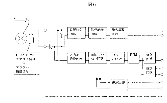
図6は、特許文献1で知られている複合伝送器の信号出力の形態を示す伝送器システム全体の構成図である。特許文献1には、複合伝送器のDC4〜20mAの主出力信号に、他のプロセス量のデジタル信号を重畳させ専用の信号変換器で、デジタル信号をアナログ信号に変換し、アナログ出力信号を複数個取り出すシステムが示されている。この例の場合、DC4〜20mAの主出力信号線にデジタル信号を重畳させるため、信号ケーブルは一対で済むという利点があるが、一般の計装用電源では機能を実現できず専用の変換器を必要とした。また、デジタル通信信号を受信しD/A変換して再発信するシステムであったため、ノイズに依る通信エラーや時間遅れなどが指摘されている。
FIG. 6 is a configuration diagram of the entire transmitter system showing a signal output form of the composite transmitter known in
図7はこれらの問題を解決するため特許文献2で提案されている伝送器システム全体の構成図であり、1つの伝送器内に複数の補助電流出力回路を備えたものである。信号ケーブルは、出力数に応じて敷設しなければならないが、一般の計装用電源でプロセス量と1対1に対応するDC4〜20mAの出力信号が得られる。しかし、この図7の例では、補助電流出力回路にはそれぞれ独立の電源回路を有しており、回路規模が大きいという難点があった。
FIG. 7 is a configuration diagram of the entire transmitter system proposed in
そして、特許文献1及び2いずれの方式も複数の電流出力とするもので、計装用電源を必要とするものであった。DC4〜20mAの信号は、信号エネルギーが大きいため、ノイズに強いとされているが、極近距離の計装配線においては、DC1〜5Vの電圧信号でも十分である。例えば、現場設置の計装盤内において伝送器の補助出力を指示計に出力する場合においては、電圧出力形であればそのまま接続可能である。しかしながら、従来方式では、このような場合においても計装用電源が必要であり、機器の費用及び配線費用が加算されることになる。
And both methods of
本発明の目的は、新たな電源回路を追加することなく、小さな回路規模によってノイズに依る通信エラーや時間遅れをなくし、出力端子がショートされたときにおいても主電流出力に影響を与えない電流制限機能を有する電圧出力回路を有する伝送器システムを提供することにある。 The object of the present invention is to eliminate a communication error and time delay due to noise without adding a new power supply circuit, and to limit current that does not affect the main current output even when the output terminal is short-circuited. An object of the present invention is to provide a transmitter system having a voltage output circuit having a function.
本発明は、複数のセンサによって検出された複数の物理量を電気信号に変換し、該電気信号が伝送線を介して負荷に伝送される電流出力回路を有する伝送器システムにおいて、前記電流出力回路に適した電源電圧を出力する電源回路に接続されアナログ電圧信号に変換され選択された前記電気信号を電流信号に変換して出力する電圧/電流出力回路を形成する主電流出力回路と、前記電源回路から電力が供給され前記主電流出力回路に並列に接続されアナログ電圧信号に変換され選択されなかった少なくとも1つの前記電気信号を電圧出力に変換して出力する第2出力用の電圧出力回路とを有することを特徴とする。 The present invention provides a transmitter system having a current output circuit that converts a plurality of physical quantities detected by a plurality of sensors into an electric signal, and the electric signal is transmitted to a load via a transmission line. A main current output circuit which forms a voltage / current output circuit which is connected to a power supply circuit which outputs a suitable power supply voltage and which is converted into an analog voltage signal to convert the selected electrical signal into a current signal for output; and the power supply circuit A voltage output circuit for a second output that is connected to the main current output circuit in parallel, is converted into an analog voltage signal, and is converted into a voltage output for output. It is characterized by having.
又、本発明は、複数のセンサによって検出された複数の物理量を電気信号に変換し、該電気信号が伝送線を介して負荷に伝送される電流出力回路を有する伝送器システムにおいて、前記電流出力回路に適した電源電圧を出力する電源回路に接続されアナログ電圧信号に変換され選択された前記電気信号を電流信号に変換して出力する電圧/電流出力回路を形成する主電流出力回路と、前記電源回路から電力が供給され前記主電流出力回路に並列に接続されアナログ電圧信号に変換され選択されなかった少なくとも1つの前記電気信号を電圧出力に変換して出力する第2出力用の電圧出力回路と、前記電源回路から電力が供給され前記主電流出力回路に並列に接続されアナログ電圧信号に変換され選択されなかった少なくとも1つの前記電気信号を電流信号に変換して出力する第2出力用の電圧/電流変換回路と、前記第2出力用の電圧出力回路と第2出力用の電圧/電流変換回路とを切り替える切り換え手段とを有することを特徴とする。 The present invention also provides a transmitter system including a current output circuit that converts a plurality of physical quantities detected by a plurality of sensors into an electric signal, and the electric signal is transmitted to a load via a transmission line. A main current output circuit that is connected to a power supply circuit that outputs a power supply voltage suitable for the circuit, converts the selected electrical signal into an analog voltage signal, converts the selected electrical signal into a current signal, and outputs the current / current output circuit; A voltage output circuit for a second output that is supplied with power from a power supply circuit, is connected in parallel to the main current output circuit, is converted into an analog voltage signal, and is converted into a voltage output for output. And at least one electrical signal that is supplied with power from the power supply circuit and connected in parallel to the main current output circuit, converted into an analog voltage signal and not selected. A second output voltage / current conversion circuit for converting the current to a current signal and switching means for switching between the second output voltage output circuit and the second output voltage / current conversion circuit. It is characterized by.
前記主電流出力回路は、前記複数の電気信号を選択するマルチプレクサと、前記電気信号を増幅するプログラマブルゲインアンプと、前記電気信号をアナログ信号からデジタル信号に変換するA/D変換回路と、前記電気信号をパルス幅変調出力する1チップマイコンと、前記パルス幅変調出力を平滑にしてアナログ電圧信号を得る平滑回路と、前記アナログ電圧信号をDC4〜20mAの電流信号に変換して出力する演算増幅器と、前記電流信号を出力する出力トランジスタとを有することが好ましい。 The main current output circuit includes a multiplexer that selects the plurality of electrical signals, a programmable gain amplifier that amplifies the electrical signals, an A / D conversion circuit that converts the electrical signals from analog signals to digital signals, and the electrical A one-chip microcomputer that outputs a pulse width modulation signal; a smoothing circuit that obtains an analog voltage signal by smoothing the pulse width modulation output; an operational amplifier that converts the analog voltage signal into a DC4 to 20 mA current signal and outputs the current signal; And an output transistor for outputting the current signal.
前記第2出力用の電圧出力回路は、前記パルス幅変調出力を平滑にしてアナログ電圧信号を得る平滑回路と、前記アナログ電圧信号をDC1〜5Vの電圧信号に変換して出力する演算増幅器と、該演算増幅器の電源端子に接続され負荷短絡時に前記演算増幅器の電源電圧を低下させて電流制限を行う電流制限抵抗器とを有することが好ましい。 The voltage output circuit for the second output includes a smoothing circuit that obtains an analog voltage signal by smoothing the pulse width modulation output, an operational amplifier that converts the analog voltage signal into a voltage signal of DC1 to 5V, and outputs the voltage signal; It is preferable to have a current limiting resistor that is connected to the power supply terminal of the operational amplifier and performs current limitation by reducing the power supply voltage of the operational amplifier when the load is short-circuited.
前記第2出力用の電圧/電流変換回路は、前記パルス幅変調出力を平滑にしてアナログ電圧信号を出力する平滑回路と、前記アナログ電圧信号をDC4〜20mAの電流信号に変換して出力する演算増幅器と、前記電流信号を出力する出力トランジスタとを有することが好ましい。 The voltage / current conversion circuit for second output smoothes the pulse width modulation output and outputs an analog voltage signal, and an operation for converting the analog voltage signal into a DC4 to 20 mA current signal and outputting it It is preferable to have an amplifier and an output transistor that outputs the current signal.
前記第2出力用の電圧/電流変換回路と第2出力用の電圧出力回路とは、いずれかの一方の回路に前記平滑回路を有することが好ましい。 The second output voltage / current conversion circuit and the second output voltage output circuit preferably include the smoothing circuit in one of the circuits.
前記DC4〜20mAの電流信号は、2線式出力を生成するデジタルアナログ変換部を有する2線式伝送器であること、前記物理量が、差圧、圧力、温度及び流量に関するプロセス量であり、該プロセス量を検出する前記センサを有することが好ましい。 The DC 4-20 mA current signal is a two-wire transmitter having a digital-analog converter that generates a two-wire output, and the physical quantity is a process quantity related to differential pressure, pressure, temperature, and flow rate, It is preferable to have the sensor for detecting the process amount.
前記1チップマイコンに複数のタイマー機能が内蔵され、該タイマーを利用してパルス幅変調出力変換することにより、複数のプロセス量をD/A変換してアナログ電圧値とし、該アナログ電圧値を前記主電流出力回路、第2出力用の電圧出力回路及び第2出力用の電圧/電流変換回路に入力することが好ましい。 A plurality of timer functions are built in the one-chip microcomputer, and a pulse width modulation output conversion is performed using the timer, whereby a plurality of process quantities are D / A converted into analog voltage values, and the analog voltage values are converted into the analog voltage values. It is preferable to input to the main current output circuit, the voltage output circuit for the second output, and the voltage / current conversion circuit for the second output.
以上のように、本発明は、複数の電圧出力形補助出力回路を設けることにより、差圧、圧力、温度信号を独立して出力できるようにしたものである。従来、通信経路で複合信号を伝送して、変換器側で、差圧、圧力、温度などの各信号に変換していたため、応答遅れや、ノイズ影響による通信障害、更に、補助電流出力回路を持つものもあったが、電流出力するためのループ電源が必要であった。これに対して、電圧出力であれば、ループ電源が不要で、補助出力を取り出すことができる。 As described above, according to the present invention, by providing a plurality of voltage output type auxiliary output circuits, differential pressure, pressure, and temperature signals can be independently output. Conventionally, a composite signal is transmitted through a communication path and converted into signals such as differential pressure, pressure, and temperature on the converter side, so communication delays due to response delays and noise effects, and an auxiliary current output circuit Some had a loop power supply to output current. On the other hand, if it is a voltage output, a loop power supply is unnecessary and an auxiliary output can be taken out.
又、本発明は、主回路の電源と、追加する電圧出力回路の演算増幅器の電源端子との間に、電流制限抵抗器を挿入することにより、出力端子ショート時に演算増幅器の電源電圧を低下させて電流制限を行うことができる。 The present invention also reduces the power supply voltage of the operational amplifier when the output terminal is short-circuited by inserting a current limiting resistor between the power supply of the main circuit and the power supply terminal of the operational amplifier of the additional voltage output circuit. Current limiting.
本伝送器システムにおいて、主電流出力の他に補助電圧出力を加えるには、マイクロプロセッサの補助出力の結果をD/A変換し、その出力を演算増幅器で電圧出力すれば良い。しかし、電圧出力形おいては、出力端子の短絡を考慮しなければならない。演算増幅器は一般に出力端子の短絡保護機能が搭載されているが、この機能は演算増幅器自身を短絡時の発熱から保護するための自衛機能で、一般に数mA〜数十mAの電流値で機能するようになっている。したがって、特に電流制限機能を設けないで演算増幅器を補助電圧出力回路に使用した場合、出力端子の短絡時には、最低でも数mAの短絡電流が流れるので、主電流出力回路の信号電流DC4〜20mAに影響を与える可能性がある。 In this transmitter system, in order to add an auxiliary voltage output in addition to the main current output, the result of the auxiliary output of the microprocessor is D / A converted, and the output is output as a voltage by an operational amplifier. However, in the voltage output type, a short circuit of the output terminal must be considered. The operational amplifier is generally equipped with a short-circuit protection function for the output terminal, but this function is a self-defense function for protecting the operational amplifier itself from the heat generated at the time of the short circuit, and generally functions at a current value of several mA to several tens mA. It is like that. Therefore, when the operational amplifier is used in the auxiliary voltage output circuit without providing a current limiting function, a short-circuit current of several mA at the minimum flows when the output terminal is short-circuited. Therefore, the signal current DC4 to 20 mA of the main current output circuit is increased. May have an impact.
電圧出力回路において電流制限をかける場合、簡単には、出力端子に抵抗器を挿入することで実現可能である。例えば、出力端子に10kΩの抵抗器を挿入した場合、5V出力時に短絡すると、短絡電流は500μAとなり、主回路の消費電流に対して許容されれば使用可能である。しかし、受信計器の入力インピーダンスは通常500kΩであるため、約2%の誤差となるため、実用にならない。 When applying a current limit in the voltage output circuit, it can be easily realized by inserting a resistor in the output terminal. For example, when a 10 kΩ resistor is inserted into the output terminal, if a short circuit occurs at the time of 5 V output, the short circuit current is 500 μA, which can be used if allowed for the consumption current of the main circuit. However, since the input impedance of the receiving instrument is usually 500 kΩ, an error of about 2% occurs, which is not practical.
本発明は、電圧出力回路の出力インピーダンスを小さく保ったまま、微小電流領域における電流制限回路を構成するため、演算増幅器の電源端子に抵抗器を挿入する構成とした。 In the present invention, a resistor is inserted into the power supply terminal of the operational amplifier in order to configure a current limiting circuit in a minute current region while keeping the output impedance of the voltage output circuit small.
本発明によれば、新たな電源回路を追加することなく、小さな回路規模によってノイズに依る通信エラーや時間遅れをなくし、出力端子がショートされたときにおいても主電流出力に影響を与えない電流制限機能を有する電圧出力回路を有する伝送器システムを得るこができる。 According to the present invention, a current limit that does not affect the main current output even when the output terminal is short-circuited without adding a new power supply circuit, eliminating a communication error or time delay due to noise due to a small circuit scale. A transmitter system having a voltage output circuit having a function can be obtained.
以下、本発明を実施するための最良の形態を具体的な実施例によって詳細に説明する。 Hereinafter, the best mode for carrying out the present invention will be described in detail by way of specific examples.
図1は、本発明の2線式複合伝送器を用いた伝送器システム全体の回路構成図である。図1に示すように、本発明の主電流出力回路20は、次の構成を有する。第1センサ1が差圧センサ、第2センサ2が圧力センサ、第3センサ3が温度センサを各々示し、各センサによって検出された物理量が電気信号に変換される。マルチプレクサ(MPX)4により第1〜第3センサ1、2、3が選択される。プログラマブルゲインアンプ(PGA)5で、選択された第1〜第3センサ1、2、3の出力信号に適した増幅率に設定し増幅する。A/D変換回路6で、第1〜第3センサ1、2、3のアナログ信号をデジタル信号に変換する。1チップマイコン7は、電気信号をパルス幅変調出力する演算機能の他、A/D制御、メモリ、通信処理、タイマー機能などを有し、温度影響補正、レンジ処理などの信号処理を行う。電源回路8で、各回路に適した電源電圧を出力する。ここでは、1出力となっているが、アナログ系、デジタル系を最適化するため2出力としても良く、必要な場合、基準電圧源も有する。平滑回路9で、1チップマイコン7のPWM(pulse width Modulation)出力(パルス幅変調出力)を平滑にしてアナログ電圧信号を得る。1チップマイコン7のPWM出力と合わせてD/A変換回路(デジタル信号をアナログ信号に変換する変換回路)を構成するものであるが、単独のD/A変換回路でも良い。電圧/電流変換回路の演算増幅器10と、電流出力用の出力トランジスタ11とで、平滑回路9で得られたアナログ電圧信号に変換された各センサからの電気信号を、DC4〜20mAの電流信号に変換して出力する。更に、本システムには、外部回路として計装用電源12、負荷抵抗13を有する。図中の2重マルは出力端子である。
FIG. 1 is a circuit configuration diagram of an entire transmitter system using the two-wire composite transmitter of the present invention. As shown in FIG. 1, the main
尚、インテリジェントタイプにおける通信機能は、演算増幅器10の入力端子に送信信号を重畳させ、電源回路の入り口から受信信号を抽出する回路に導くことにより可能であるが、この図では除いてある。
The communication function in the intelligent type is possible by superimposing a transmission signal on the input terminal of the
図1においては、第2出力用の電圧出力回路30は1つであるが、前述のセンサの数と同じ数の第2出力用の電圧出力回路を設けることができ、これらの第2出力用の電圧出力回路は第2出力用の電圧出力回路30を全く同じ電圧出力回路を電源回路8から電源が供給され主電流出力回路20に並列に第3出力用、第4出力用の電圧出力回路を形成することができる。
In FIG. 1, the number of
次に、本発明の第2出力用の電圧出力回路構成30を説明する。第2出力用の平滑回路109は、第2出力信号のD/A変換を行う。本実施例の1チップマイコン7は、複数個のタイマーを有しているため、部品の追加なしで、第2のPWM出力を得ることができる。そのため、簡単な平滑回路109を追加するだけで第2出力のアナログ電圧信号を得ることができる。演算増幅器110は第2出力用の電圧出力回路である。電流制限用抵抗器200は、主回路の電源回路と演算増幅器110の電源端子との間に挿入され、第2の電圧出力回路の出力端子120、121を有する。図中の2重丸は出力端子である。
Next, the voltage
図2は、本発明の伝送器システムにおける第2出力用の電圧出力回路の動作を説明するための図である。動作は、主回路の電源回路8から電源供給を受け、出力端子ショート時に電流制限が働き、第1出力に影響を及ぼさない第2出力用の電圧出力回路を構成することができる。
FIG. 2 is a diagram for explaining the operation of the voltage output circuit for the second output in the transmitter system of the present invention. In operation, a power supply is supplied from the
なお、電圧出力端子ショート時の消費電流は、供給電源電圧Vsと電流制限抵抗器200により決まり、さらに小さくすることも可能である。例えば、供給電源電圧Vsを6Vとして、電流制限抵抗器200を30kΩとすれば、200μA以下にすることができる。
The current consumption when the voltage output terminal is short-circuited is determined by the supply power supply voltage Vs and the current limiting
ここで、使用する演算増幅器110は、低消費電流タイプのものを使用し、数10μA程度で動作可能であり、例えば、20μAとする。そして、電流制限抵抗器200を10kΩ、回路への供給電源電圧Vsを5.5Vとすると、電流制限抵抗器200の電圧降下は0.2Vとなり、演算増幅器110の電源電圧は、5.3Vとなる。ここで使用する演算増幅器110を、入出力信号電圧範囲がほぼ電源電圧範囲まで追従可能な、いわゆるRail-to-Railタイプのものとすると、演算増幅器110は、約5.3Vまで出力可能である。
Here, the
ここで、演算増幅器110の出力を5V、負荷抵抗13を500kΩとした場合、負荷抵抗13に流れる電流は10μAとなる。そして、負荷電流とほぼ同じ電流が演算増幅器110の消費電流の増加となり、約30μAとなる。すると、電流制限抵抗器200の電圧降下は、0.3Vとなり、演算増幅器の電源電圧は5.2Vとなるため、5Vを出力することは可能である。
Here, when the output of the
次に、この状態で負荷抵抗13を100kΩとすると、負荷抵抗13に流れる電流は50μA、演算増幅器110の消費電流は約70μAとなる。すると、電流制限抵抗器200の電圧降下は約0.7Vとなり、演算増幅器110の電源電圧は4.8Vとなり出力電圧5Vより小さくなり不合理を生ずる。したがって、この場合、出力電圧は演算増幅器110の電源電圧で制限され、5V以下の電圧とならなければならない。そして、負荷抵抗13に流れる電流も50μAよりも小さくなる。このようにして、徐々に電流制限が働く。そして、最も極端な場合として、負荷抵抗13が0Ωつまり出力端子がショートした場合、消費電流の最大値は、電流制限抵抗200で制限され、5.5V/10kΩ=550μAよりも大きくなることはない。
Next, assuming that the
表1は、図2に示す本発明の第2出力用の電圧出力回路を用いた負荷抵抗を変化させて消費電流を測定した実験結果を示すものである。表1に示すように、第2出力用の電圧出力回路として、負荷抵抗500kΩまで正常動作し、出力端子ショート時の消費電流359μAという特性のものを得ることができた。 Table 1 shows the experimental results of measuring the current consumption by changing the load resistance using the voltage output circuit for the second output of the present invention shown in FIG. As shown in Table 1, the voltage output circuit for the second output was able to operate normally up to a load resistance of 500 kΩ and had a characteristic of current consumption of 359 μA when the output terminal was short-circuited.
以上のように、本実施例によれば、2線式伝送器の回路に電圧出力換回路を付加するだけで、容易に追加の電圧出力回路を構成できるという利点がある。又、2線式伝送器の信号処理には、ワンチップマイコンが使用される。そして、汎用のワンチップマイコン7には、複数のタイマー機能が内蔵されているので、このタイマーを利用してPWM変換することにより、他のプロセス量を容易にD/A変換して電圧値とすることができる。この電圧値となった他のプロセス量を、前述の電圧出力換回路に入力することにより、複数の電圧出力回路を持つ伝送器とすることができる。
As described above, according to the present embodiment, there is an advantage that an additional voltage output circuit can be easily configured only by adding a voltage output conversion circuit to the circuit of the two-wire transmitter. A one-chip microcomputer is used for signal processing of the two-wire transmitter. Since the general-purpose one-
本実施例によれば、新たな電源回路を追加することなく、小さな回路規模によってノイズに依る通信エラーや時間遅れをなくし、出力端子がショートされたときにおいても主電流出力に影響を与えない電流制限機能を有する電圧出力回路を有する伝送器システムを得ることができる。 According to the present embodiment, a current that does not affect the main current output even when the output terminal is short-circuited without adding a new power supply circuit, eliminating a communication error or time delay due to noise with a small circuit scale. A transmitter system having a voltage output circuit having a limiting function can be obtained.
図4は、本発明の伝送器システム全体の回路構成図である。本実施例は、第2出力用の電圧出力回路と、電源回路8から電力が供給され主電流出力回路に並列に接続されアナログ電圧信号に変換され選択されなかった少なくとも1つの電気信号を電流信号に変換して出力する第2出力用の電圧/電流変換回路と、第2出力用の電圧出力回路と第2出力用の電圧/電流変換回路とを切り替える切り換え手段122とを有する伝送器システムである。図4に示すように、本発明の主電流出力回路20及び第2出力用の電圧出力回路30は、実施例1と全く同様であり、そして実施例1の伝送器システムに第2出力用の電圧/電流変換回路40を加えて、第2出力用の電圧出力回路30と切り換え手段122によって切り替えて使用するものである。
FIG. 4 is a circuit configuration diagram of the entire transmitter system of the present invention. In the present embodiment, a voltage output circuit for second output and at least one electric signal supplied with power from the
本発明の第2出力用の電圧/電流変換回路40は、主電流出力回路20に並列に電源回路8から電源が供給され少なくとも1つの電流出力回路を形成する。以下、その第2出力用の電圧/電流変換回路40の構成について説明する。第2出力用の平滑回路2(109)で、第2出力信号のD/A変換を行う。1チップマイコン7は、複数個のタイマーを有しており、部品の追加なしで、第2のPWM出力を得ることができる。そのため、簡単な平滑回路2(109)を追加するだけで第2出力のアナログ電圧信号を得ることができる。平滑回路2(109)は第2出力用の電圧出力回路30と第2出力用の電圧/電流変換回路40と共用される。電源は、電源回路8を通して供給される。
The second output voltage /
本システムには、第2出力用の電圧/電流出力回路40の演算増幅器110、第2出力回路の出力トランジスタ111を有し、外部回路として第2出力用の計装電源112、負荷抵抗113を有する。
This system includes an
図4においては、第2出力用の電圧出力回路30と第2出力用の電圧/電流変換回路40とは1つであるが、前述のセンサの数に応じて設けることができ、これらの第2出力用の電圧出力回路30と第2出力用の電圧/電流変換回路40とを全く同じように電源回路8から電源が供給され主電流出力回路20に並列に第3出力用、第4出力用の電圧出力回路と電圧/電流変換回路を形成することができる。
In FIG. 4, the number of the
図5は、第2出力用の電圧/電流変換回路の消費電流を説明するための回路構成図である。図5において、第2出力用の電圧/電流変換回路への供給電源電流は、演算増幅器110への供給電流Isである。演算増幅器110に供給された電流Isは、演算増幅器110自身の動作電流Iss、出力トランジスタを駆動するための出力電流Io、そして入力バイアス電流Ib+、Ib−に分流される。演算増幅器110自身の動作電流は、演算増幅器110のマイナス電源端子から主回路の電源マイナスに戻る。
FIG. 5 is a circuit configuration diagram for explaining current consumption of the voltage / current conversion circuit for the second output. In FIG. 5, the power supply current supplied to the voltage / current conversion circuit for the second output is the supply current Is to the
出力電流Ioは、出力トランジスタ111のベース電流として流れ、エミッタから出てエミッタ抵抗Reを経由して、主回路電源マイナスに戻る。そして、入力バイアス電流のうちIb−は、入力マイナス端子から出て、主回路電源マイナスに戻る。入力バイアス電流Ib+は、入力抵抗Rsに流れ込むものIb+1と、帰還抵抗Rfに流れ込むものIb+2に分流するが、Rsに流れ込む電流Ib+1は平滑回路を経由して主回路電源マイナスに戻り、Rfに流れ込む電流Ib+2は出力電流検出抵抗Roを経由して主回路電源マイナスに戻る。以上のようにして、演算増幅器110への供給電流は、図中の点線のように、すべて主回路電源マイナスに戻り、電流の収支バランスがとられる。
The output current Io flows as the base current of the
したがって、第2出力用の電圧/電流変換回路40を設けた場合、演算増幅器110への電源電流が増加するだけで、主電流出力回路20の出力電流値へ影響を与えることはない。そして、第2出力用の電圧/電流変換回路40の消費電流は、高々100μAで構成することができるので、従来形の回路に容易に回路を追加して、複数の電流出力回路を有する伝送器を構成することができる。
Therefore, when the voltage /
本実施例においては、従来の2線式伝送器の回路に第2出力用の電圧/電流変換回路40を付加するだけで、容易に追加の電流出力回路を構成できるという利点がある。又、2線式伝送器の信号処理には、ワンチップマイコン7が使用され、汎用のワンチップマイコン7には、複数のタイマー機能が内蔵されているので、このタイマーを利用してPWM変換することにより、他のプロセス量を容易にD/A変換してアナログ電圧値とすることができる。このアナログ電圧値となった他のプロセス量を、第2出力用の電圧/電流変換回路に入力することにより、複数の電流出力回路を持つ伝送器とすることができる。
In the present embodiment, there is an advantage that an additional current output circuit can be easily configured simply by adding the voltage /
ここで、主電流出力回路20における電圧/電流変換回路の消費電流は、使用する演算増幅器10の消費電流と出力トランジスタ11を駆動するためのベース電流である。演算増幅器10については、低消費電流タイプのものが使用され、例えば、50μAとする。
Here, the consumption current of the voltage / current conversion circuit in the main
また、電流出力トランジスタ11のベース電流は、使用するトランジスタの電流増幅率に依存するが、電流出力トランジスタはダーリントンタイプあるいはハイβ(高電流増幅率)タイプのものが使用され、電流増幅率は1,000以上である。すると、出力電流20mAのときのベース電流は、20μAとなる。ただし、出力端子に電源が接続されない場合、出力回路にループ電流は流れないが、第2出力用の電圧/電流変換回路40の演算増幅器110は、フィードバック制御の安定点まで電流を流そうとする動作をするため、出力端子の電圧は最大値まで振り切れる。このとき、ベース電流は最大値となり、出力トランジスタのベース抵抗とVbeそして演算増幅器の最大出力電圧で決まる電流が流れる。例えば、演算増幅器の電源電圧が5V、最大出力電圧が4.5V、出力トランジスタの電流増幅率が1,000、Vbeが0.7Vのとき、ベース抵抗は190kΩ以下であれば最大出力電流20mAを駆動できる。余裕をみて100kΩとした場合、出力端子開放時のベース電流は、38μAとなる。したがって、演算増幅器の動作電流50μAと合わせて、88μAの消費電流となる。以上のようにして、第2出力用の電圧/電流変換回路の消費電流は100μA程度で設計することができる。
The base current of the
本実施例においても、新たな電源回路を追加することなく、主電流出力回路20に、第2出力用の電圧出力回路30と第2出力用の電圧/電流変換回路40とを加えて、切り換え手段122によって切り替えて使用することにより、小さな回路規模によってノイズに依る通信エラーや時間遅れをなくし、又、出力端子がショートされたときにおいても主電流出力に影響を与えない電流制限機能を有する電圧出力回路あるいは、出力端子がオープンになったときにおいても主電流出力に影響を与えない電流出力回路を有する伝送器システムを得ることができる。
Also in this embodiment, without adding a new power supply circuit, the
1…第1センサ、2…第2センサ、3…第3センサ、4…マルチプレクサ(MPX)、5…プログラマブルゲインアンプ(PGA)、6…A/D変換回路、7…1チップマイコン、8…電源回路、9…平滑回路1、10,110…演算増幅器、11…出力トランジスタ、12…計装用電源、13…負荷抵抗、20…主電流出力回路、30…第2出力用の電圧出力回路、40…第2出力用の電圧/電流変換回路、109…平滑回路2、200…電流制限抵抗器、120、121…電圧出力の出力端子、122…切り換え手段。
DESCRIPTION OF
Claims (10)
7. The method according to claim 2, wherein a plurality of timer functions are built in the one-chip microcomputer, and a plurality of process quantities are D / A converted to analog by performing pulse width modulation output conversion using the timer. A transmitter system comprising: a voltage value; and the analog voltage value is input to the main current output circuit, the second output voltage output circuit, and the second output voltage / current conversion circuit.
Priority Applications (1)
| Application Number | Priority Date | Filing Date | Title |
|---|---|---|---|
| JP2006154100A JP2007323450A (en) | 2006-06-02 | 2006-06-02 | Transmitter system |
Applications Claiming Priority (1)
| Application Number | Priority Date | Filing Date | Title |
|---|---|---|---|
| JP2006154100A JP2007323450A (en) | 2006-06-02 | 2006-06-02 | Transmitter system |
Publications (1)
| Publication Number | Publication Date |
|---|---|
| JP2007323450A true JP2007323450A (en) | 2007-12-13 |
Family
ID=38856190
Family Applications (1)
| Application Number | Title | Priority Date | Filing Date |
|---|---|---|---|
| JP2006154100A Pending JP2007323450A (en) | 2006-06-02 | 2006-06-02 | Transmitter system |
Country Status (1)
| Country | Link |
|---|---|
| JP (1) | JP2007323450A (en) |
Cited By (3)
| Publication number | Priority date | Publication date | Assignee | Title |
|---|---|---|---|---|
| JP2010261901A (en) * | 2009-05-11 | 2010-11-18 | Daiichi Keiki Seisakusho Co Ltd | Thermometer |
| JP2011511382A (en) * | 2008-02-06 | 2011-04-07 | ローズマウント インコーポレイテッド | Digitally compensated process transmitter with minimal dead time |
| CN105388816A (en) * | 2015-12-28 | 2016-03-09 | 天津市森特尔新技术有限公司 | Extensible high-voltage detection control unit |
-
2006
- 2006-06-02 JP JP2006154100A patent/JP2007323450A/en active Pending
Cited By (4)
| Publication number | Priority date | Publication date | Assignee | Title |
|---|---|---|---|---|
| JP2011511382A (en) * | 2008-02-06 | 2011-04-07 | ローズマウント インコーポレイテッド | Digitally compensated process transmitter with minimal dead time |
| JP2010261901A (en) * | 2009-05-11 | 2010-11-18 | Daiichi Keiki Seisakusho Co Ltd | Thermometer |
| CN105388816A (en) * | 2015-12-28 | 2016-03-09 | 天津市森特尔新技术有限公司 | Extensible high-voltage detection control unit |
| CN105388816B (en) * | 2015-12-28 | 2017-12-12 | 天津市森特尔新技术有限公司 | A kind of expansible high pressure detection control unit |
Similar Documents
| Publication | Publication Date | Title |
|---|---|---|
| JP5222015B2 (en) | Field equipment | |
| JP5141790B2 (en) | 2-wire transmitter | |
| CN111045369B (en) | Auxiliary control circuit of power amplifier module, power amplifier module and communication equipment | |
| US10740272B2 (en) | Input circuit that can be made redundant, input circuit unit having at least one input circuit, and method for operating the input circuit unit | |
| JP2014092414A (en) | Thermal-type flowmeter | |
| US11222526B2 (en) | Two-wire transmitter | |
| WO2013153599A1 (en) | Sequencer analog output unit | |
| JP5462062B2 (en) | Electromagnetic flow meter | |
| JP2007323450A (en) | Transmitter system | |
| JP4888714B2 (en) | Voltage applied current measurement circuit | |
| JP2004085288A (en) | Multivariable transmitter | |
| JP2007323449A (en) | Transmitter system | |
| CN101359874B (en) | Driver circuits for converters with intermediate circuits | |
| US10302678B2 (en) | Motor control circuitry | |
| JP4830058B2 (en) | 2-wire transmitter | |
| CN223362546U (en) | Current output circuit and numerical control constant current source | |
| JP4534544B2 (en) | Transmitter system | |
| JPH0535619Y2 (en) | ||
| JP4989594B2 (en) | Digital protection controller | |
| CN108983859A (en) | Programmable power supply | |
| JPH039229A (en) | Burn-out circuit for thermocouple | |
| JP2010060351A (en) | Signal input circuit | |
| JP2009048328A (en) | 2-wire transmitter | |
| CN118392027A (en) | Voltage-current conversion circuit and current output type angle sensor | |
| JP4894996B2 (en) | Field indicator |