JP2007242951A - Barrier film for semiconductor wiring, copper wiring for semiconductor, manufacturing method of this wiring, and sputtering target for forming semiconductor barrier film - Google Patents
Barrier film for semiconductor wiring, copper wiring for semiconductor, manufacturing method of this wiring, and sputtering target for forming semiconductor barrier film Download PDFInfo
- Publication number
- JP2007242951A JP2007242951A JP2006064343A JP2006064343A JP2007242951A JP 2007242951 A JP2007242951 A JP 2007242951A JP 2006064343 A JP2006064343 A JP 2006064343A JP 2006064343 A JP2006064343 A JP 2006064343A JP 2007242951 A JP2007242951 A JP 2007242951A
- Authority
- JP
- Japan
- Prior art keywords
- copper
- film
- semiconductor
- wiring
- barrier film
- Prior art date
- Legal status (The legal status is an assumption and is not a legal conclusion. Google has not performed a legal analysis and makes no representation as to the accuracy of the status listed.)
- Withdrawn
Links
- 230000004888 barrier function Effects 0.000 title claims abstract description 131
- 239000010949 copper Substances 0.000 title claims abstract description 117
- 229910052802 copper Inorganic materials 0.000 title claims abstract description 84
- RYGMFSIKBFXOCR-UHFFFAOYSA-N Copper Chemical compound [Cu] RYGMFSIKBFXOCR-UHFFFAOYSA-N 0.000 title claims abstract description 83
- 239000004065 semiconductor Substances 0.000 title claims abstract description 48
- 238000005477 sputtering target Methods 0.000 title claims abstract description 10
- 238000004519 manufacturing process Methods 0.000 title claims description 19
- 229910000599 Cr alloy Inorganic materials 0.000 claims abstract description 34
- 239000012535 impurity Substances 0.000 claims abstract description 17
- 238000004544 sputter deposition Methods 0.000 claims abstract description 17
- 230000035699 permeability Effects 0.000 claims abstract description 10
- 239000010410 layer Substances 0.000 claims description 94
- 238000007747 plating Methods 0.000 claims description 19
- 239000000758 substrate Substances 0.000 claims description 18
- 239000011247 coating layer Substances 0.000 claims description 16
- 239000011248 coating agent Substances 0.000 claims description 2
- 238000000576 coating method Methods 0.000 claims description 2
- 239000010408 film Substances 0.000 abstract description 111
- 238000009792 diffusion process Methods 0.000 abstract description 29
- 238000010438 heat treatment Methods 0.000 abstract description 6
- 229910052804 chromium Inorganic materials 0.000 abstract description 5
- 230000000694 effects Effects 0.000 abstract description 4
- 239000010409 thin film Substances 0.000 abstract description 3
- 239000000203 mixture Substances 0.000 description 24
- 238000000682 scanning probe acoustic microscopy Methods 0.000 description 18
- 230000000052 comparative effect Effects 0.000 description 12
- 239000000654 additive Substances 0.000 description 10
- 230000000996 additive effect Effects 0.000 description 10
- 229910004298 SiO 2 Inorganic materials 0.000 description 9
- 229910052751 metal Inorganic materials 0.000 description 9
- 239000000463 material Substances 0.000 description 8
- 239000002184 metal Substances 0.000 description 8
- 229910045601 alloy Inorganic materials 0.000 description 7
- 239000000956 alloy Substances 0.000 description 7
- UFHFLCQGNIYNRP-UHFFFAOYSA-N Hydrogen Chemical compound [H][H] UFHFLCQGNIYNRP-UHFFFAOYSA-N 0.000 description 6
- 229910018487 Ni—Cr Inorganic materials 0.000 description 6
- 238000000137 annealing Methods 0.000 description 6
- 238000009713 electroplating Methods 0.000 description 6
- 239000007789 gas Substances 0.000 description 6
- 239000001307 helium Substances 0.000 description 6
- 229910052734 helium Inorganic materials 0.000 description 6
- SWQJXJOGLNCZEY-UHFFFAOYSA-N helium atom Chemical compound [He] SWQJXJOGLNCZEY-UHFFFAOYSA-N 0.000 description 6
- 239000001257 hydrogen Substances 0.000 description 6
- 229910052739 hydrogen Inorganic materials 0.000 description 6
- 238000012545 processing Methods 0.000 description 6
- 239000013078 crystal Substances 0.000 description 5
- 229910000838 Al alloy Inorganic materials 0.000 description 3
- QVGXLLKOCUKJST-UHFFFAOYSA-N atomic oxygen Chemical compound [O] QVGXLLKOCUKJST-UHFFFAOYSA-N 0.000 description 3
- 230000008859 change Effects 0.000 description 3
- 239000001301 oxygen Substances 0.000 description 3
- 229910052760 oxygen Inorganic materials 0.000 description 3
- 239000002245 particle Substances 0.000 description 3
- 238000005498 polishing Methods 0.000 description 3
- 238000005488 sandblasting Methods 0.000 description 3
- 229910000531 Co alloy Inorganic materials 0.000 description 2
- 238000004458 analytical method Methods 0.000 description 2
- 230000015572 biosynthetic process Effects 0.000 description 2
- 238000001816 cooling Methods 0.000 description 2
- 238000007772 electroless plating Methods 0.000 description 2
- 238000005242 forging Methods 0.000 description 2
- 229910052738 indium Inorganic materials 0.000 description 2
- APFVFJFRJDLVQX-UHFFFAOYSA-N indium atom Chemical compound [In] APFVFJFRJDLVQX-UHFFFAOYSA-N 0.000 description 2
- 239000011229 interlayer Substances 0.000 description 2
- 239000012528 membrane Substances 0.000 description 2
- 238000000034 method Methods 0.000 description 2
- 230000005012 migration Effects 0.000 description 2
- 238000013508 migration Methods 0.000 description 2
- 238000005096 rolling process Methods 0.000 description 2
- 239000000126 substance Substances 0.000 description 2
- 230000003746 surface roughness Effects 0.000 description 2
- 229910000881 Cu alloy Inorganic materials 0.000 description 1
- 239000004642 Polyimide Substances 0.000 description 1
- 229910052776 Thorium Inorganic materials 0.000 description 1
- 229910001069 Ti alloy Inorganic materials 0.000 description 1
- 229910052770 Uranium Inorganic materials 0.000 description 1
- 230000008901 benefit Effects 0.000 description 1
- 230000005540 biological transmission Effects 0.000 description 1
- 238000005219 brazing Methods 0.000 description 1
- 239000004020 conductor Substances 0.000 description 1
- 230000007423 decrease Effects 0.000 description 1
- 230000007547 defect Effects 0.000 description 1
- 230000009977 dual effect Effects 0.000 description 1
- 238000005516 engineering process Methods 0.000 description 1
- 238000005530 etching Methods 0.000 description 1
- 238000005755 formation reaction Methods 0.000 description 1
- 239000011261 inert gas Substances 0.000 description 1
- 238000005259 measurement Methods 0.000 description 1
- 238000012986 modification Methods 0.000 description 1
- 230000004048 modification Effects 0.000 description 1
- 229910052750 molybdenum Inorganic materials 0.000 description 1
- 229910052759 nickel Inorganic materials 0.000 description 1
- 229920001721 polyimide Polymers 0.000 description 1
- 230000008569 process Effects 0.000 description 1
- 238000011160 research Methods 0.000 description 1
- 238000003892 spreading Methods 0.000 description 1
- 230000007480 spreading Effects 0.000 description 1
- 229920006259 thermoplastic polyimide Polymers 0.000 description 1
- 229920005992 thermoplastic resin Polymers 0.000 description 1
- 229910052719 titanium Inorganic materials 0.000 description 1
- 238000003466 welding Methods 0.000 description 1
Images


Landscapes
- Physical Vapour Deposition (AREA)
- Electrodes Of Semiconductors (AREA)
- Internal Circuitry In Semiconductor Integrated Circuit Devices (AREA)
Abstract
Description
本発明は、銅の拡散を効果的に抑制することのできる半導体配線用バリア膜、半導体用銅配線、同配線の製造方法及び半導体バリア膜形成用スパッタリングターゲットに関する。 The present invention relates to a barrier film for semiconductor wiring, a copper wiring for semiconductor, a manufacturing method of the wiring, and a sputtering target for forming a semiconductor barrier film that can effectively suppress copper diffusion.
従来、半導体ウエハー上に形成する高密度集積回路の微細な配線材料として、アルミニウム系合金に代わり高速化が可能な銅が用いられるようになってきた。銅は、比抵抗が1.8μWcmと低くエレクトロマイグレーション耐性がアルミニウム合金系と比較して一桁高いという特徴を有している。
ところで、半導体装置には素子間を接続するトレンチやビアが多数形成されており、これらは層間絶縁層に開口部を形成し、そこに導電性材料を埋め込むことにより形成される。近年、その層間絶縁層に溝部を形成し、銅で溝部を埋め込むことで溝配線を形成するシングルダマシン法、あるいは銅で溝部および溝部の底部に設けられた開口部を埋め込むことで、トレンチとビアホールを一体に形成するデュアルダマシン法による配線形成が実用化されつつある。
集積回路の内部では、金属配線が何層にも張り巡らされて信号を伝送しているが、高密度化に伴い配線間の距離が近くなるに伴い、前記トレンチやビア内に形成した銅が容易に拡散し(マイグレーション)、回路配線が短絡するという問題が発生するようになった。
Conventionally, as a fine wiring material of a high-density integrated circuit formed on a semiconductor wafer, copper capable of increasing the speed has been used instead of an aluminum alloy. Copper has a characteristic that the specific resistance is as low as 1.8 μWcm and the electromigration resistance is one digit higher than that of the aluminum alloy system.
By the way, many trenches and vias for connecting elements are formed in a semiconductor device, and these are formed by forming an opening in an interlayer insulating layer and embedding a conductive material therein. In recent years, trenches and via holes have been formed by forming a trench in the interlayer insulating layer and filling the trench with copper to form a trench wiring, or by embedding the trench and the opening provided at the bottom of the trench with copper. Wiring formation by a dual damascene method in which the two are integrally formed is being put into practical use.
Inside an integrated circuit, metal wiring is stretched over several layers to transmit signals. However, as the distance between wirings becomes shorter as the density increases, the copper formed in the trenches and vias becomes smaller. The problem of easy diffusion (migration) and short-circuiting of circuit wiring has occurred.
このようなCuの拡散を抑制するために、トレンチやビアの下に予めCuの拡散を防止するためのバリア層を形成し、その上にCuのシード層及びCuの厚付けめっき層を形成することが提案されている。
その代表的なものとして、Ni−Cr合金のバリア層を形成したものがある(特許文献1参照)。
しかし、200〜300°C程度の温度上昇があると、依然としてCuの拡散が認められる。また、特に配線幅が狭くなると、従来のバリア層では銅の拡散を防ぐことができず、必ずしも効果的でないことが分かった。
In order to suppress such diffusion of Cu, a barrier layer for preventing diffusion of Cu is previously formed under the trench or via, and a Cu seed layer and a Cu thick plating layer are formed thereon. It has been proposed.
A typical example is a Ni-Cr alloy barrier layer formed (see Patent Document 1).
However, if there is a temperature rise of about 200 to 300 ° C., diffusion of Cu is still recognized. Further, it has been found that when the wiring width becomes narrow, the conventional barrier layer cannot prevent copper diffusion and is not necessarily effective.
これを防ぐ手段として、従来のバリア層の厚さを厚くすることで、バリア特性を向上させることも考えられる。しかし、一定値以上に厚さを厚くすると、配線幅を狭くできないという問題が発生した。したがって、これも根本的な解決手段とは言えなかった。
本技術に近いものとしてポリイミドのフレキシブル回路基板への応用例があり、Ni、Cr、Co、Moから選んだ少なくとも1種の金属からなるバリアメタルを被覆し、熱可塑性樹脂を加熱して流動化させ、熱可塑性ポリイミドとバリアメタルとの結合力を増加させるという提案もある(特許文献2参照)。
しかし、この場合は、バリアメタルの拡散というものの根本的なものを解決するものではないので、依然として問題は残っている。
There is an application example of polyimide to a flexible circuit board that is close to this technology, coating a barrier metal made of at least one metal selected from Ni, Cr, Co, and Mo, and fluidizing by heating a thermoplastic resin There is also a proposal to increase the bonding force between the thermoplastic polyimide and the barrier metal (see Patent Document 2).
However, in this case, the problem remains because it does not solve the fundamental barrier metal diffusion.
以上の従来技術の問題点から、トレンチやビアを埋め込んで形成された銅の拡散を抑制するに際し、膜剥離を生じさせない程度の薄い膜厚で、また狭い配線幅でも十分なバリア効果を得ることができ、さらに熱処理等により温度上昇があっても、バリア特性に変化がない半導体回路形成用バリア膜及びバリア膜形成用スパッタリングターゲットを得ることを課題とする。 Due to the above-mentioned problems of the prior art, when suppressing the diffusion of copper formed by burying trenches and vias, a sufficient barrier effect can be obtained with a thin film thickness that does not cause film peeling and a narrow wiring width. It is another object of the present invention to obtain a barrier film for forming a semiconductor circuit and a sputtering target for forming a barrier film that do not change in barrier characteristics even when the temperature rises due to heat treatment or the like.
本発明者らは鋭意研究を行った結果、効果的なバリア特性を有する合金を使用し、バリア膜をできる限り薄くして剥離を防止すると共に、成膜した膜の均一性を高めることにより、上記の課題を解決することができるとの知見を得た。 As a result of diligent research, the present inventors have used an alloy having effective barrier properties, made the barrier film as thin as possible to prevent peeling, and improve the uniformity of the film formed, The knowledge that said subject can be solved was acquired.
本発明はこの知見に基づき、
1. Crを5〜30wt%含有し、残部が不可避的不純物及びCoからなるCo−Cr合金膜からなり、膜厚が3〜150nm、膜厚均一性が1σで10%以下であることを特徴とする半導体配線用バリア膜
2. 半導体基板上に、膜厚が3〜150nm、膜厚均一性が1σで10%以下であるCo−Cr合金からなるバリア膜、及び該バリア膜上に形成された銅被覆層を備えていることを特徴とする半導体用銅配線
3. Co−Cr合金からなるバリア膜が、Crを5〜30wt%含有し、残部が不可避的不純物及びCoからなるCo−Cr合金膜であることを特徴とする上記2記載の半導体用銅配線
4. バリア膜上に形成された銅被覆層が、無電解銅めっき層又は無電解銅めっきシード層とその上に形成された電気銅めっき層であることを特徴とする上記2又は3記載の半導体用銅配線
5. バリア膜上に形成された銅被覆層が、銅スパッタ膜又は銅スパッタ膜からなるシード層とその上に形成された電気銅めっき層であることを特徴とする上記2又は3記載の半導体用銅配線、を提供する。
The present invention is based on this finding,
1. It is characterized in that it contains 5 to 30 wt% of Cr, the balance is a Co—Cr alloy film made of inevitable impurities and Co, the film thickness is 3 to 150 nm, and the film thickness uniformity is 10% or less at 1σ. 1. Barrier film for semiconductor wiring Provided on a semiconductor substrate is a barrier film made of a Co—Cr alloy having a film thickness of 3 to 150 nm and a film thickness uniformity of 10% or less at 1σ, and a copper coating layer formed on the barrier film. 2. Copper wiring for semiconductors characterized by 3. The copper wiring for a semiconductor according to 2 above, wherein the barrier film made of a Co—Cr alloy is a Co—Cr alloy film containing 5 to 30 wt% of Cr and the balance being made of inevitable impurities and Co. The copper coating layer formed on the barrier film is an electroless copper plating layer or an electroless copper plating seed layer and an electrolytic copper plating layer formed thereon. 4. Copper wiring 4. The copper for semiconductor according to the above 2 or 3, wherein the copper coating layer formed on the barrier film is a copper sputtered film or a seed layer made of a copper sputtered film and an electro copper plating layer formed thereon. Wiring, provide.
本発明は、また
6. 半導体基板上に、スパッタリングによりCo−Cr合金からなるバリア膜を形成し、さらにその上に無電解銅めっき層又は無電解銅めっきシード層と電気銅めっきによる銅被覆層を形成することを特徴とする半導体用配線の製造方法
7. 半導体基板上に、スパッタリングによりCo−Cr合金からなるバリア膜を形成し、さらにその上にスパッタ銅被覆層又はスパッタ膜からなる銅シード層と電気銅めっきによる銅被覆層を形成することを特徴とする半導体用配線の製造方法
8. Co−Cr合金からなるバリア膜は、膜厚が3〜150nm、膜厚均一性が1σで10%以下であることを特徴とする上記6又は7記載の半導体用銅配線の製造方法
9. Co−Cr合金からなるバリア膜が、Crを5〜30wt%含有し、残部が不可避的不純物及びCoからなるCo−Cr合金膜であることを特徴とする上記6〜8のいずれかに記載の半導体用銅配線の製造方法
10.Crを5〜30wt%含有し、残部が不可避的不純物及びCoからなるCo−Cr合金であって、スパッタ面の面内方向の比透磁率が100以下であることを特徴とする半導体バリア膜形成用スパッタリングターゲット、を提供する。
The present invention also provides: A barrier film made of a Co—Cr alloy is formed on a semiconductor substrate by sputtering, and an electroless copper plating layer or an electroless copper plating seed layer and a copper coating layer by electrolytic copper plating are further formed thereon. 6. Manufacturing method of semiconductor wiring to be performed A barrier film made of a Co-Cr alloy is formed on a semiconductor substrate by sputtering, and a copper seed layer made of a sputtered copper coating layer or a sputtered film and a copper coating layer formed by electrolytic copper plating are further formed thereon. Manufacturing method for semiconductor wiring 8. 8. The method for producing a copper wiring for a semiconductor according to 6 or 7 above, wherein the barrier film made of a Co—Cr alloy has a film thickness of 3 to 150 nm and a film thickness uniformity of 10% or less at 1σ. The barrier film made of a Co—Cr alloy contains 5 to 30 wt% of Cr, and the balance is a Co—Cr alloy film made of inevitable impurities and Co. 9. Manufacturing method of copper wiring for semiconductor Co-Cr alloy containing 5 to 30 wt% of Cr, the balance being inevitable impurities and Co, and having a relative permeability in the in-plane direction of the sputtering surface of 100 or less, forming a semiconductor barrier film A sputtering target is provided.
本発明の半導体銅配線用バリア膜は、膜剥離を生じさせない程度の薄い膜厚とし、また狭い配線幅でも十分なバリア効果を得ることができ、さらに熱処理等により温度上昇があっても、バリア特性に変化がないという優れた特徴を有している。本発明は、半導体銅配線材料において銅の拡散を効果的に抑制する著しい特性を有する。 The barrier film for semiconductor copper wiring of the present invention has a thin film thickness that does not cause film peeling, and can obtain a sufficient barrier effect even with a narrow wiring width. It has an excellent feature that there is no change in characteristics. The present invention has significant characteristics that effectively suppress copper diffusion in semiconductor copper wiring materials.
本発明の半導体銅配線材料用バリア膜は、Crを5〜30wt%含有し、残部が不可避的不純物及びCoからなるCo−Cr合金膜である。
膜組成において、Crが5wt%に満たない場合はバリア性が十分でなく、従来のバリア膜に比べ優位性が無い。また、Crが30wt%を超えると、CMP(ケミカルメカニカルポリッシング)加工する際、このバリア膜がポリッシングを阻害するので、除去するのに非常に時間がかかり過ぎ、実用に向かない。したがって、上記のCrの範囲とする。
The barrier film for semiconductor copper wiring material of the present invention is a Co—Cr alloy film containing 5 to 30 wt% of Cr and the balance being inevitable impurities and Co.
In the film composition, when Cr is less than 5 wt%, the barrier property is not sufficient, and there is no advantage over the conventional barrier film. On the other hand, if the Cr content exceeds 30 wt%, this barrier film hinders polishing during CMP (Chemical Mechanical Polishing), so that it takes too much time to remove and is not suitable for practical use. Therefore, the Cr range is set.
本発明の半導体銅配線材料用バリア膜の膜厚は、3〜150nmとする。膜厚が3nm未満の場合:充分なバリア性を持たない。また、膜厚が150nmを超えると膜剥がれを生じ易くなるので、上記の範囲とする。
本発明の半導体銅配線材料用バリア膜の膜厚は、膜厚均一性が1σで10%以下とする。膜厚均一性(1σ)が、10%を超えると、バリア膜上に形成する銅膜が不均一となり、半導体の伝送特性に支障をきたすという問題がある。このことにより、実デバイスの耐久性が低下する。したがって、上記の膜厚均一性(1σ)を10%以下とする。
The thickness of the barrier film for semiconductor copper wiring material of the present invention is 3 to 150 nm. When the film thickness is less than 3 nm: it does not have sufficient barrier properties. Moreover, since it will become easy to produce film peeling when a film thickness exceeds 150 nm, it is set as said range.
The film thickness of the barrier film for semiconductor copper wiring material of the present invention is 10% or less with a film thickness uniformity of 1σ. If the film thickness uniformity (1σ) exceeds 10%, the copper film formed on the barrier film becomes non-uniform, which causes a problem in that the transmission characteristics of the semiconductor are hindered. This reduces the durability of the actual device. Therefore, the film thickness uniformity (1σ) is set to 10% or less.
本発明のバリア膜形成用スパッタリングターゲットについては、Crを5〜30wt%含有し、残部が不可避的不純物及びCoからなるCo−Cr合金ターゲットを用いる。本発明のCo−Cr合金ターゲットの組成は、バリア膜の組成に直接反映される。すなわち、ターゲット組成のCrが5wt%に満たない場合、5wt%Cr以上のCo合金膜が成膜できない。
一方Crが30wt%を超えると、Cr30%以下Co合金の膜が成膜できない。したがって、Co−Cr合金ターゲットの組成は、上記の範囲とする。
また、本発明のバリア膜形成用スパッタリングターゲットの、スパッタ面の面内方向の比透磁率が100以下とする。比透磁率が100を超えると、スパッタ膜の膜厚均一性が1σで10%を超えてしまうからである。
For the sputtering target for forming a barrier film of the present invention, a Co—Cr alloy target containing 5 to 30 wt% of Cr and the balance of inevitable impurities and Co is used. The composition of the Co—Cr alloy target of the present invention is directly reflected in the composition of the barrier film. That is, when the target composition Cr is less than 5 wt%, a Co alloy film of 5 wt% Cr or more cannot be formed.
On the other hand, if Cr exceeds 30 wt%, a film of Co alloy of
Further, the relative permeability in the in-plane direction of the sputtering surface of the sputtering target for forming a barrier film of the present invention is set to 100 or less. This is because when the relative magnetic permeability exceeds 100, the film thickness uniformity of the sputtered film exceeds 10% at 1σ.
本発明のCo−Cr合金ターゲットは、平均結晶粒径が500μm以下、特に100μm以下が望ましい。平均結晶粒径が500μmを超えると、パーティクル発生量多くなり、ピンホールと呼ばれる膜欠陥が増加し、製品収率が低下するからである。
また、本発明のCo−Cr合金ターゲットは、ターゲット内の平均結晶粒径のバラツキが30%以内のものが望ましい。平均粒径のばらつきが30%を超えると、スパッタ成膜した膜の膜厚均一性が1σで10%を超えるおそれがあるからである。
The Co—Cr alloy target of the present invention preferably has an average crystal grain size of 500 μm or less, particularly 100 μm or less. This is because when the average crystal grain size exceeds 500 μm, the amount of particles generated increases, film defects called pinholes increase, and the product yield decreases.
In addition, the Co—Cr alloy target of the present invention desirably has an average crystal grain size variation within 30% within the target. This is because if the variation in average particle diameter exceeds 30%, the film thickness uniformity of the sputtered film may exceed 10% at 1σ.
本発明のターゲットを製造するに際しては、800〜1370°Cの熱間における鍛造と、圧延の組み合わせにより、ターゲット板に加工するのが望ましい。
さらに、前記熱間鍛造・圧延後、大気中、真空中又は不活性ガス雰囲気中で、保持温度:300〜960°Cの熱処理を行うのが良い。
これによって得た熱処理板をターゲット形状に加工し、スパッタリングされる面の平均粗さ (Ra) を、0.01〜5μmとする。
また、ターゲットやバッキングプレートの側面などの非スパッタ面、すなわちスパッタされた物質が付着する部分を、サンドブラスト処理、エッチング処理又は溶射被膜層の形成等によって、表面の平均粗さ (Ra)を1〜50μmに表面粗化して、付着した被膜が再剥離するのを防止することが望ましい。再剥離してスパッタ雰囲気中に浮遊する物質は、基板へのパーティクル発生の原因となるからである。
When manufacturing the target of the present invention, it is desirable to process the target plate by a combination of hot forging at 800 to 1370 ° C. and rolling.
Further, after the hot forging / rolling, heat treatment at a holding temperature of 300 to 960 ° C. may be performed in the air, in a vacuum, or in an inert gas atmosphere.
The heat-treated plate thus obtained is processed into a target shape, and the average roughness (Ra) of the surface to be sputtered is set to 0.01 to 5 μm.
In addition, the average roughness (Ra) of the surface of the non-sputtered surface such as the side surface of the target or backing plate, that is, the portion to which the sputtered material adheres, is reduced by sandblasting, etching, or formation of a sprayed coating layer. It is desirable to roughen the surface to 50 μm to prevent the attached film from peeling again. This is because the substance that re-peels and floats in the sputtering atmosphere causes generation of particles on the substrate.
本発明のターゲットは、高出力スパッタに耐えられるように、Al合金、Cu、 Cu合金、Ti、Ti合金などのバッキングプレートへ、ロウ付け若しくは、拡散接合法や摩擦圧接法などの金属結合によってボンディングすることが望ましい。
また、ターゲットに含有される不純物として、Na、Kの濃度がそれぞれ5ppm以下(以降ppmは、wtppmを示す)、U、Thの濃度がそれぞれ0.05ppm以下、さらには主元素、添加元素以外の金属元素の総計が0.5wt%以下、かつ酸素濃度が0.5%以下であることが望ましい。
The target of the present invention is bonded to a backing plate made of Al alloy, Cu, Cu alloy, Ti, Ti alloy or the like by brazing or metal bonding such as diffusion bonding or friction welding so that it can withstand high power sputtering. It is desirable to do.
Further, as impurities contained in the target, the concentrations of Na and K are each 5 ppm or less (hereinafter, ppm indicates wtppm), the concentrations of U and Th are each 0.05 ppm or less, and other than the main elements and additive elements It is desirable that the total amount of metal elements is 0.5 wt% or less and the oxygen concentration is 0.5% or less.
本発明の半導体用配線の製造に際しては、半導体基板上に、スパッタリングによりCo−Cr合金からなるバリア膜を形成し、さらにその上に無電解めっき層又は無電解めっきシード層と電気銅めっきによる銅被覆層を形成して高密度の半導体用配線を形成することができる。本発明のバリア膜は、このような集積度の高い配線膜においても、半導体基板への銅の拡散を効果的に抑制できる。
上記のCo−Cr合金からなるバリア膜を形成した後、さらにその上にスパッタ銅被覆層又はスパッタ膜からなる銅シード層と電気銅めっきによる銅被覆層を形成することもできる。これは製造工程に応じて、適宜選択できる。
前記Co−Cr合金からなるバリア膜を形成する場合には、いずれも膜厚が3〜150nm、膜厚均一性が1σで10%以下であることが必要である。また、このバリア膜はCrを5〜30wt%含有し、残部が不可避的不純物及びCoからなるCo−Cr合金膜であることが望ましい。
以上のCo−Cr合金のバリア膜はスパッタリングにより形成するが、スパッタ面の面内方向の比透磁率が100以下である半導体バリア膜形成用スパッタリングターゲットを使用することが望ましい。
In manufacturing the semiconductor wiring of the present invention, a barrier film made of a Co—Cr alloy is formed on a semiconductor substrate by sputtering, and an electroless plating layer or an electroless plating seed layer and copper by electrolytic copper plating are further formed thereon. A coating layer can be formed to form a high-density semiconductor wiring. The barrier film of the present invention can effectively suppress the diffusion of copper into the semiconductor substrate even in such a highly integrated wiring film.
After the barrier film made of the Co—Cr alloy is formed, a sputtered copper coating layer or a copper seed layer made of the sputtered film and a copper coating layer by electrolytic copper plating can be further formed thereon. This can be appropriately selected according to the manufacturing process.
In the case of forming a barrier film made of the Co—Cr alloy, it is necessary that the film thickness is 3 to 150 nm and the film thickness uniformity is 10% or less at 1σ. The barrier film is preferably a Co—Cr alloy film containing 5 to 30 wt% of Cr and the balance being inevitable impurities and Co.
Although the above Co—Cr alloy barrier film is formed by sputtering, it is desirable to use a sputtering target for forming a semiconductor barrier film having a relative permeability of 100 or less in the in-plane direction of the sputtering surface.
次に、実施例に基づいて本発明を説明する。以下に示す実施例は、理解を容易にするためのものであり、これらの実施例によって本発明を制限するものではない。本発明の技術思想に基づく変形及び他の実施例は、当然本発明に含まれる。すなわち、以下に示す実施例は、好適な実施例の一部を示しているだけで、以下の実施例だけに本発明が限定される必要がないことは容易に理解されるべきものである。 Next, the present invention will be described based on examples. The following examples are for ease of understanding, and the present invention is not limited by these examples. Modifications and other embodiments based on the technical idea of the present invention are naturally included in the present invention. That is, it should be easily understood that the following examples show only some of the preferred examples, and the present invention is not limited to the following examples.
(実施例1)
Co−20wt%Crの組成を溶解・鋳造し、Co−Crインゴットを作製した。これを、1100°Cで熱間鍛造・熱間圧延し、冷却後500°Cで2時間熱処理を行い、ターゲットに加工した。このターゲットの結晶粒径は280μmであった。これを、さらに表面の平均粗さ:Raを0.14μmに仕上げた。
ターゲット中のCr濃度は19.1wt%で、不純物成分は、Na:0.2ppm、K:0.1ppm、U:0.02ppm、Th:0.03ppm、 金属成分の総計が470ppm、 酸素が10ppmであった。
このターゲットをバッキングプレートにインジウムでボンディングして、ターゲットの側面とターゲット近傍のバッキングプレート部をサンドブラストで、Ra=7.5μmに粗化した。
Example 1
A composition of Co-20 wt% Cr was melted and cast to prepare a Co-Cr ingot. This was hot forged and hot rolled at 1100 ° C., and after cooling, heat-treated at 500 ° C. for 2 hours to be processed into a target. The crystal grain size of this target was 280 μm. This was further finished with an average surface roughness: Ra of 0.14 μm.
The Cr concentration in the target is 19.1 wt%, the impurity components are Na: 0.2 ppm, K: 0.1 ppm, U: 0.02 ppm, Th: 0.03 ppm, the total of metal components is 470 ppm, and oxygen is 10 ppm. Met.
This target was bonded to the backing plate with indium, and the side surface of the target and the backing plate near the target were roughened to Ra = 7.5 μm by sand blasting.
このターゲットを使って、8インチのSiO2基板上に、膜厚:140nmのバリア層を作製した。このバリア層の各添加成分の組成を分析したところ、Cr:18.3wt%と、若干Crが少ない組成と一致した。このバリア層の膜厚を49点測定し、その膜厚均一性を調べたところ、1σで7.2%であった。
このバリア層の上に、スパッタリングにより200nmのCuを成膜した。
このCu/Co−Cr積層膜について、成膜したままの試料と、真空中で 300°C×2時間の熱処理を行った試料について、AES(オージェ電子分光法)で深さ方向にプロファイルをとり、Cuのバリア層への拡散を評価した。
図1に、AESの結果を示す。Co−Crをバリア膜としたものでは、 300°Cで熱処理したものでも、Cuのプロファイルは熱処理を行わなかったものと同様のプロファイルを示しており、バリア層への拡散が認められなかった。
Using this target, a barrier layer having a thickness of 140 nm was formed on an 8-inch SiO 2 substrate. When the composition of each additive component of this barrier layer was analyzed, it coincided with Cr: 18.3 wt%, which was slightly less Cr. When the film thickness of this barrier layer was measured at 49 points and the film thickness uniformity was examined, it was 7.2% at 1σ.
On this barrier layer, 200 nm of Cu was deposited by sputtering.
About this Cu / Co-Cr laminated film, a profile was taken in the depth direction by AES (Auger Electron Spectroscopy) for the as-deposited sample and the sample heat-treated at 300 ° C for 2 hours in vacuum. The diffusion of Cu into the barrier layer was evaluated.
FIG. 1 shows the results of AES. In the case where Co—Cr was used as the barrier film, the Cu profile showed the same profile as that obtained when the heat treatment was not performed, and diffusion into the barrier layer was not observed.
(比較例1)
従来のバリア材であるNi−20wt%Crの組成を有する材料を、溶解・鋳造し、Ni−Crインゴットを作製した。これを、1100°Cで熱間鍛造・熱間圧延し、冷却後500°Cで2時間の熱処理を行い、ターゲットに加工した。
このターゲットの結晶粒径は300μmで、表面粗さをRaで0.15μmに仕上げた。ターゲット中のCr濃度は19.7wt%、不純物成分は、Na: 0.1ppm、K:0.3ppm、U:0.02ppm、Th:0.04ppm、 不純物金属成分の総計が510ppm、 酸素が10ppmであった。
(Comparative Example 1)
A material having a composition of Ni-20 wt% Cr, which is a conventional barrier material, was melted and cast to prepare a Ni-Cr ingot. This was hot forged and hot rolled at 1100 ° C., and after cooling, heat-treated at 500 ° C. for 2 hours to be processed into a target.
The crystal grain size of this target was 300 μm, and the surface roughness was finished to 0.15 μm with Ra. Cr concentration in the target is 19.7 wt%, impurity components are Na: 0.1 ppm, K: 0.3 ppm, U: 0.02 ppm, Th: 0.04 ppm, the total of impurity metal components is 510 ppm, oxygen is 10 ppm Met.
ターゲットをバッキングプレートにインジウムでボンディングして、ターゲットの側面とターゲット近傍のバッキングプレート部をサンドブラストで、Ra=7.0μmに粗化した。ターゲットの面内方向の比透磁率は130であった。
このターゲットを使って、SiO2基板上に膜厚:140nmのバリア層を作製した。
このバリア層の各添加成分の組成を分析したところ、Cr:18.5wt%と、若干Crが少ない組成となった。このバリア層の膜厚を49点測定し、その膜厚均一性を調べたところ、1σで7.4%であった。
The target was bonded to the backing plate with indium, and the side surface of the target and the backing plate near the target were roughened to Ra = 7.0 μm by sandblasting. The relative permeability in the in-plane direction of the target was 130.
Using this target, a barrier layer having a thickness of 140 nm was formed on a SiO 2 substrate.
When the composition of each additive component of the barrier layer was analyzed, Cr was 18.5 wt%, and the composition was slightly less Cr. When the film thickness of this barrier layer was measured at 49 points and the film thickness uniformity was examined, it was 7.4% at 1σ.
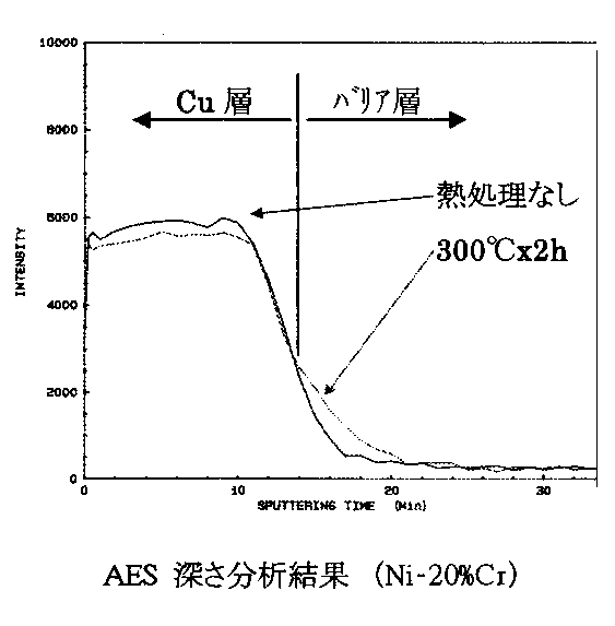
このバリア層の上にスパッタ法でCu膜を200nm成膜した。このCu/ Ni−Cr膜について、成膜したままの試料と、真空中で300°C×2時間の熱処理を行った試料について、AES(オージェ電子分光法)で深さ方向にプロファイルをとり、Cuのバリア層への拡散を評価した。図2にAESの結果を示す。
300°Cで熱処理したもののCuのプロファイルが、熱処理していないものよりも、バリア層に入り込んでいる。すなわち、バリア層としての機能が低いことが分かった。
A Cu film having a thickness of 200 nm was formed on the barrier layer by sputtering. About this Cu / Ni-Cr film, about the sample as it was formed and the sample which performed heat processing for 300 ° C x 2 hours in a vacuum, take a profile in the depth direction by AES (Auger electron spectroscopy), The diffusion of Cu into the barrier layer was evaluated. FIG. 2 shows the results of AES.
The Cu profile that was heat-treated at 300 ° C. entered the barrier layer more than the one that was not heat-treated. That is, it turned out that the function as a barrier layer is low.
(実施例2〜8)
上記実施例1と同様の製造方法を用いてターゲットを製造し、下記表1に示す本発明の範囲にある合金組成及び比透磁率のターゲットを用いて、8インチのSiO2基板上に、膜厚10nmのバリア層を形成した。
さらに、このバリア層の各添加成分の組成(wt%)、バリア層の膜厚(nm)及びバリア層の膜厚を49点測定し、その膜厚の均一性(%)を調べた。その結果を表1に示す。実施例2〜8のバリア膜の膜組成(wt%)、膜厚(nm)、膜厚の均一性(%)はいずれも、本願発明の範囲に入るものである。
さらに、このバリア層の上にスパッタ法でCuシード層を20nm成膜後、電気めっきにより200nmのCu層を形成した。そして、2%水素/98%ヘリウムガス雰囲気において400℃30分間のアニール処理を行った。熱処理を行った試料について、AES(オージェ電子分光法)で深さ方向にプロファイルをとり、熱処理前後の比較により、Cuバリア層への拡散を評価した。この結果、銅の拡散は認められなかった。これらの結果を同様に、表1に示す。
以上の結果、実施例2〜8は、いずれも銅のマイグレーションは見られなかった。
(Examples 2 to 8)
A target was manufactured using the same manufacturing method as in Example 1 above, and a film was formed on an 8-inch SiO 2 substrate using an alloy composition and relative permeability target within the scope of the present invention shown in Table 1 below. A 10 nm thick barrier layer was formed.
Further, the composition (wt%) of each additive component of the barrier layer, the film thickness (nm) of the barrier layer, and the film thickness of the barrier layer were measured at 49 points, and the uniformity (%) of the film thickness was examined. The results are shown in Table 1. The film composition (wt%), film thickness (nm), and film thickness uniformity (%) of the barrier films of Examples 2 to 8 all fall within the scope of the present invention.
Further, a Cu seed layer having a thickness of 20 nm was formed on the barrier layer by sputtering, and then a 200 nm Cu layer was formed by electroplating. Then, annealing was performed at 400 ° C. for 30 minutes in a 2% hydrogen / 98% helium gas atmosphere. About the sample which heat-processed, the profile was taken in the depth direction by AES (Auger electron spectroscopy), and the diffusion to Cu barrier layer was evaluated by the comparison before and behind heat processing. As a result, no copper diffusion was observed. These results are similarly shown in Table 1.
As a result, no migration of copper was observed in any of Examples 2 to 8.
(比較例2)
表1に示す上記比較例1と同一のターゲットを用いて、8インチのSiO2基板上に、膜厚10nmのNi−Crバリア層を形成した。
さらに、このバリア層の各添加成分の組成(wt%)、バリア層の膜厚(nm)及びバリア層の膜厚を49点測定し、その膜厚の均一性(%)を調べた。その結果を表1に示す。比較例2のバリア膜の合金成分(Ni−Cr)は、本願発明と異なるものである。
さらに、このバリア層の上にCuシード層を20nm成膜後、電気めっきにより200nmのCu層を形成した。そして、2%水素/98%ヘリウムガス雰囲気において400°C30分間のアニール処理を行った。熱処理を行った試料について、AES(オージェ電子分光法)で深さ方向にプロファイルをとり、熱処理前後の比較により、Cuバリア層への拡散を評価した。この結果、銅の拡散が認められた。これらの結果を同様に、表1に示す。
(Comparative Example 2)
Using the same target as in Comparative Example 1 shown in Table 1, a 10 nm thick Ni—Cr barrier layer was formed on an 8-inch SiO 2 substrate.
Further, the composition (wt%) of each additive component of the barrier layer, the thickness of the barrier layer (nm), and the thickness of the barrier layer were measured at 49 points, and the uniformity (%) of the thickness was examined. The results are shown in Table 1. The alloy component (Ni-Cr) of the barrier film of Comparative Example 2 is different from the present invention.
Further, a Cu seed layer was formed to 20 nm on the barrier layer, and then a 200 nm Cu layer was formed by electroplating. Then, annealing was performed at 400 ° C. for 30 minutes in a 2% hydrogen / 98% helium gas atmosphere. About the sample which heat-processed, the profile to the depth direction was taken with AES (Auger electron spectroscopy), and the diffusion to Cu barrier layer was evaluated by the comparison before and behind heat processing. As a result, copper diffusion was observed. These results are similarly shown in Table 1.
(比較例3)
上記実施例1と同様の製造方法を用いてターゲットを製造し、下記表1に示す本発明外の範囲にある合金組成(Cr量が本願発明よりも少ない)のターゲットを用いて、8インチのSiO2基板上に、膜厚10nmのCo−Crバリア層を形成した。
さらに、このバリア層の各添加成分の組成(Cr3.5wt%)、バリア層の膜厚(nm)及びバリア層の膜厚を49点測定し、その膜厚の均一性(%)を調べた。その結果を表1に示す。
比較例3のバリア膜の膜組成(Cr3.5wt%)は、本願発明の膜のCr含有量(5〜30wt%)よりも少ない。
さらに、このバリア層の上にCuシード層を20nm成膜後、電気めっきにより200nmのCu層を形成した。そして、2%水素/98%ヘリウムガス雰囲気において400°C30分間のアニール処理を行った。熱処理を行った試料について、AES(オージェ電子分光法)で深さ方向にプロファイルをとり、熱処理前後の比較により、Cuバリア層への拡散を評価した。この結果、銅の拡散が認められた。これらの結果を同様に、表1に示す。
(Comparative Example 3)
Using the same manufacturing method as in Example 1 above, a target was manufactured, and an alloy composition (Cr amount smaller than that of the present invention) in the range outside the present invention shown in Table 1 below was used. A Co—Cr barrier layer having a thickness of 10 nm was formed on the SiO 2 substrate.
Further, the composition of each additive component of the barrier layer (Cr 3.5 wt%), the thickness of the barrier layer (nm), and the thickness of the barrier layer were measured at 49 points, and the uniformity (%) of the thickness was examined. . The results are shown in Table 1.
The film composition (Cr 3.5 wt%) of the barrier film of Comparative Example 3 is less than the Cr content (5 to 30 wt%) of the film of the present invention.
Further, a Cu seed layer was formed to 20 nm on the barrier layer, and then a 200 nm Cu layer was formed by electroplating. Then, annealing was performed at 400 ° C. for 30 minutes in a 2% hydrogen / 98% helium gas atmosphere. About the sample which heat-processed, the profile to the depth direction was taken with AES (Auger electron spectroscopy), and the diffusion to Cu barrier layer was evaluated by the comparison before and behind heat processing. As a result, copper diffusion was observed. These results are similarly shown in Table 1.
(比較例4)
上記実施例1と同様の製造方法を用いてターゲットを製造し、下記表1に示す本発明外の範囲にある合金組成(Cr量が本願発明よりも多い)のターゲットを用いて、SiO2基板上に、膜厚10nmのCo−Crバリア層を形成した。
さらに、このバリア層の各添加成分の組成(Cr33.1wt%)、バリア層の膜厚(nm)及びバリア層の膜厚を49点測定し、その膜厚の均一性(%)を調べた。その結果を表1に示す。
比較例3のバリア膜の膜組成(Cr33.1wt%)は、本願発明の膜のCr含有量(5〜30wt%)よりも多い。
さらに、このバリア層の上にCuシード層を20nm成膜後、電気めっきにより200nmのCu層を形成した。そして、2%水素/98%ヘリウムガス雰囲気において400°C30分間のアニール処理を行った。熱処理を行った試料について、CMPによるポリッシングを試みたが均一性に問題があった。これらの結果を同様に、表1に示す。
(Comparative Example 4)
A target was manufactured using the same manufacturing method as in Example 1 above, and an SiO 2 substrate was prepared using a target having an alloy composition (Cr amount larger than that of the present invention) in the range outside the present invention shown in Table 1 below. A Co—Cr barrier layer having a thickness of 10 nm was formed thereon.
Further, the composition of each additive component of the barrier layer (Cr 33.1 wt%), the thickness of the barrier layer (nm), and the thickness of the barrier layer were measured at 49 points, and the uniformity (%) of the thickness was examined. . The results are shown in Table 1.
The film composition (Cr 33.1 wt%) of the barrier film of Comparative Example 3 is larger than the Cr content (5 to 30 wt%) of the film of the present invention.
Further, a Cu seed layer was formed to 20 nm on the barrier layer, and then a 200 nm Cu layer was formed by electroplating. Then, annealing was performed at 400 ° C. for 30 minutes in a 2% hydrogen / 98% helium gas atmosphere. Polishing by CMP was attempted on the heat-treated sample, but there was a problem with uniformity. These results are similarly shown in Table 1.
(比較例5)
上記実施例1と同様の製造方法を用いてターゲットを製造し、下記表1に示す通りターゲットの比透磁率が本発明外にあるターゲットを用いて、SiO2基板上に、膜厚10nmのCo−Crバリア層を形成した。
さらに、このバリア層の各添加成分の組成、バリア層の膜厚(nm)及びバリア層の膜厚を49点測定し、その膜厚の均一性(%)を調べた。その結果を表1に示す。
さらに、このバリア層の上にCuシード層を20nm成膜後、電気めっきにより200nmのCu層を形成した。そして、2%水素/98%ヘリウムガス雰囲気において400°C30分間のアニール処理を行った。熱処理を行った試料について、AES(オージェ電子分光法)で深さ方向にプロファイルをとり、熱処理前後の比較により、Cuバリア層への拡散を評価した。この結果、銅の拡散が認められた。これらの結果を同様に、表1に示す。
(Comparative Example 5)
A target was manufactured using the same manufacturing method as in Example 1, and a target having a relative permeability outside the present invention as shown in Table 1 below was used on a SiO 2 substrate with a film thickness of 10 nm. A Cr barrier layer was formed.
Further, the composition of each additive component of the barrier layer, the thickness (nm) of the barrier layer, and the thickness of the barrier layer were measured at 49 points, and the uniformity (%) of the thickness was examined. The results are shown in Table 1.
Further, a Cu seed layer was formed to 20 nm on the barrier layer, and then a 200 nm Cu layer was formed by electroplating. Then, annealing was performed at 400 ° C. for 30 minutes in a 2% hydrogen / 98% helium gas atmosphere. About the sample which heat-processed, the profile to the depth direction was taken with AES (Auger electron spectroscopy), and the diffusion to Cu barrier layer was evaluated by the comparison before and behind heat processing. As a result, copper diffusion was observed. These results are similarly shown in Table 1.
(比較例6)
上記実施例1と同様の製造方法を用いてターゲットを製造し、下記表1に示すターゲットを用いてスパッタリングし、SiO2基板上に、膜厚が本発明外にある 2.5nm(本願発明より薄い)のCo−Crバリア層を形成した。
このバリア層の各添加成分の組成、ターゲットの比透磁率、膜組成及びバリア層の膜厚を49点測定し、膜厚の均一性(%)を調べた。その結果を表1に示す。
さらに、このバリア層の上にCuシード層を20nm成膜後、電気めっきにより200nmのCu層を形成した。そして、2%水素/98%ヘリウムガス雰囲気において400°C30分間のアニール処理を行った。熱処理を行った試料について、AES(オージェ電子分光法)で深さ方向にプロファイルをとり、熱処理前後の比較により、Cuバリア層への拡散を評価した。この結果、銅の拡散が認められた。これらの結果を同様に、表1に示す。バリア層の膜厚が十分でない場合にはCuの拡散が起り、耐久性がないことが分かった。
(Comparative Example 6)
To produce a target using the same manufacturing method as in Example 1, by sputtering using a target shown in Table 1, the SiO 2 substrate, than 2.5 nm (the present invention the film thickness is outside the present invention A thin) Co—Cr barrier layer was formed.
The composition of each additive component of the barrier layer, the relative permeability of the target, the film composition, and the film thickness of the barrier layer were measured at 49 points, and the film thickness uniformity (%) was examined. The results are shown in Table 1.
Further, a Cu seed layer was formed to 20 nm on the barrier layer, and then a 200 nm Cu layer was formed by electroplating. Then, annealing was performed at 400 ° C. for 30 minutes in a 2% hydrogen / 98% helium gas atmosphere. About the sample which heat-processed, the profile was taken in the depth direction by AES (Auger electron spectroscopy), and the diffusion to Cu barrier layer was evaluated by the comparison before and behind heat processing. As a result, copper diffusion was observed. These results are similarly shown in Table 1. When the thickness of the barrier layer was not sufficient, it was found that Cu diffusion occurred and there was no durability.
(比較例7)
上記実施例1と同様の製造方法を用いて表1に示すターゲットを製造し、下記表1に示す通りバリア層の膜厚が本発明外にある条件で、8インチのSiO2基板上に、膜厚が本発明外にある180nm(本願発明より厚い)のCo−Crバリア層を形成した。
さらに、このバリア層の各添加成分の組成及びバリア層の膜厚(nm)を、同様に表1に示す。しかし、このバリア層は剥離したため、その後の測定は不能となった。以上から、バリア層の過剰な膜厚は、適切でないことが分かった。
(Comparative Example 7)
Using the same manufacturing method as in Example 1 above, the targets shown in Table 1 were manufactured. On the condition that the thickness of the barrier layer was outside the present invention as shown in Table 1 below, on an 8-inch SiO 2 substrate, A Co—Cr barrier layer having a thickness of 180 nm (thicker than that of the present invention) outside the present invention was formed.
Further, the composition of each additive component of the barrier layer and the thickness (nm) of the barrier layer are also shown in Table 1. However, since this barrier layer was peeled off, subsequent measurement was impossible. From the above, it was found that an excessive film thickness of the barrier layer is not appropriate.
本発明は、狭い配線幅の銅回路でも十分なバリア効果を得ることができ、さらに熱処理等による温度上昇があっても、バリア特性に変化がないという優れた特徴を有している。このように、銅の拡散を効果的に抑制する著しい特性を有するので、高密度銅配線半導体用バリア膜として有用である。 The present invention has an excellent feature that a sufficient barrier effect can be obtained even with a copper circuit with a narrow wiring width, and even if the temperature rises due to heat treatment or the like, the barrier characteristics do not change. Thus, since it has the remarkable characteristic which suppresses the spreading | diffusion of copper effectively, it is useful as a barrier film for high-density copper wiring semiconductors.
Claims (10)
Co-Cr alloy containing 5 to 30 wt% of Cr, the balance being inevitable impurities and Co, and having a relative permeability in the in-plane direction of the sputtering surface of 100 or less, forming a semiconductor barrier film Sputtering target.
Priority Applications (1)
| Application Number | Priority Date | Filing Date | Title |
|---|---|---|---|
| JP2006064343A JP2007242951A (en) | 2006-03-09 | 2006-03-09 | Barrier film for semiconductor wiring, copper wiring for semiconductor, manufacturing method of this wiring, and sputtering target for forming semiconductor barrier film |
Applications Claiming Priority (1)
| Application Number | Priority Date | Filing Date | Title |
|---|---|---|---|
| JP2006064343A JP2007242951A (en) | 2006-03-09 | 2006-03-09 | Barrier film for semiconductor wiring, copper wiring for semiconductor, manufacturing method of this wiring, and sputtering target for forming semiconductor barrier film |
Publications (1)
| Publication Number | Publication Date |
|---|---|
| JP2007242951A true JP2007242951A (en) | 2007-09-20 |
Family
ID=38588188
Family Applications (1)
| Application Number | Title | Priority Date | Filing Date |
|---|---|---|---|
| JP2006064343A Withdrawn JP2007242951A (en) | 2006-03-09 | 2006-03-09 | Barrier film for semiconductor wiring, copper wiring for semiconductor, manufacturing method of this wiring, and sputtering target for forming semiconductor barrier film |
Country Status (1)
| Country | Link |
|---|---|
| JP (1) | JP2007242951A (en) |
Cited By (2)
| Publication number | Priority date | Publication date | Assignee | Title |
|---|---|---|---|---|
| JP2011214039A (en) * | 2010-03-31 | 2011-10-27 | Sanyo Special Steel Co Ltd | Method for producing sputtering target material |
| JP4961023B2 (en) * | 2007-12-21 | 2012-06-27 | Jx日鉱日石金属株式会社 | Copper foil for printed wiring boards |
-
2006
- 2006-03-09 JP JP2006064343A patent/JP2007242951A/en not_active Withdrawn
Cited By (2)
| Publication number | Priority date | Publication date | Assignee | Title |
|---|---|---|---|---|
| JP4961023B2 (en) * | 2007-12-21 | 2012-06-27 | Jx日鉱日石金属株式会社 | Copper foil for printed wiring boards |
| JP2011214039A (en) * | 2010-03-31 | 2011-10-27 | Sanyo Special Steel Co Ltd | Method for producing sputtering target material |
Similar Documents
| Publication | Publication Date | Title |
|---|---|---|
| JP4466925B2 (en) | Barrier film for flexible copper substrate and sputtering target for barrier film formation | |
| JP4996639B2 (en) | Sputter target | |
| JP3403918B2 (en) | High purity copper sputtering target and thin film | |
| JP2010502841A (en) | Copper sputtering target having very small crystal grain size and high electromigration resistance and method for producing the same | |
| JPWO1995016797A1 (en) | Mo-W material for forming wiring, Mo-W target for forming wiring and its manufacturing method, and Mo-W thin wiring film | |
| US20070039817A1 (en) | Copper-containing pvd targets and methods for their manufacture | |
| TWI397125B (en) | Semiconductor device manufacturing method | |
| JP2000034562A (en) | Sputtering target and thin film forming equipment parts | |
| JP5638697B2 (en) | High purity copper chrome alloy sputtering target | |
| JP2006041128A (en) | Cu-based wiring forming method for semiconductor device | |
| JP2017088984A (en) | Ag ALLOY FILM, MANUFACTURING METHOD OF Ag ALLOY FILM, AND Ag ALLOY SPUTTERING TARGET | |
| JP2004193553A (en) | Copper alloy sputtering target for forming semiconductor device wiring seed layer and seed layer formed using the target | |
| JP4825345B2 (en) | Sputtering target, barrier layer using the same, and method of forming electronic device | |
| JP2007242951A (en) | Barrier film for semiconductor wiring, copper wiring for semiconductor, manufacturing method of this wiring, and sputtering target for forming semiconductor barrier film | |
| JP3898043B2 (en) | Sputtering target and semiconductor device and sputtering apparatus using the same | |
| JP4005295B2 (en) | Manufacturing method of semiconductor device | |
| JP2007242947A (en) | Barrier film for semiconductor wiring, copper wiring for semiconductor, manufacturing method of this wiring, and sputtering target for forming semiconductor barrier film | |
| JP2004193552A (en) | Copper alloy sputtering target for seed layer formation of semiconductor device wiring | |
| JP4485570B2 (en) | Barrier film for flexible copper substrate and sputtering target for barrier film formation | |
| JP2008288574A (en) | Cu wiring of semiconductor device and manufacturing method thereof | |
| JP2004193546A (en) | Copper alloy sputtering target for seed layer formation of semiconductor device wiring | |
| US9909196B2 (en) | High-purity copper-cobalt alloy sputtering target | |
| JP2007126748A (en) | Manufacturing method of high purity Ta material for semiconductor device | |
| JPH11176769A (en) | Sputtering target and copper wiring film | |
| JP4421586B2 (en) | Method for producing sputtering target and method for producing copper wiring film |
Legal Events
| Date | Code | Title | Description |
|---|---|---|---|
| A300 | Withdrawal of application because of no request for examination |
Free format text: JAPANESE INTERMEDIATE CODE: A300 Effective date: 20090512 |