JP2007165501A - Surface emitting semiconductor laser and manufacturing method thereof - Google Patents
Surface emitting semiconductor laser and manufacturing method thereof Download PDFInfo
- Publication number
- JP2007165501A JP2007165501A JP2005358569A JP2005358569A JP2007165501A JP 2007165501 A JP2007165501 A JP 2007165501A JP 2005358569 A JP2005358569 A JP 2005358569A JP 2005358569 A JP2005358569 A JP 2005358569A JP 2007165501 A JP2007165501 A JP 2007165501A
- Authority
- JP
- Japan
- Prior art keywords
- layer
- mirror
- region
- semiconductor layer
- semiconductor laser
- Prior art date
- Legal status (The legal status is an assumption and is not a legal conclusion. Google has not performed a legal analysis and makes no representation as to the accuracy of the status listed.)
- Withdrawn
Links
- 239000004065 semiconductor Substances 0.000 title claims abstract description 262
- 238000004519 manufacturing process Methods 0.000 title claims abstract description 22
- 239000000203 mixture Substances 0.000 claims description 178
- 238000000034 method Methods 0.000 claims description 36
- 238000005530 etching Methods 0.000 claims description 12
- 239000013078 crystal Substances 0.000 claims description 9
- 239000012535 impurity Substances 0.000 claims description 4
- 238000012544 monitoring process Methods 0.000 claims description 4
- 238000010030 laminating Methods 0.000 claims 1
- 239000000758 substrate Substances 0.000 abstract description 15
- 230000007423 decrease Effects 0.000 abstract description 10
- 230000010355 oscillation Effects 0.000 abstract description 10
- 229910052782 aluminium Inorganic materials 0.000 abstract description 7
- XAGFODPZIPBFFR-UHFFFAOYSA-N aluminium Chemical compound [Al] XAGFODPZIPBFFR-UHFFFAOYSA-N 0.000 abstract description 7
- 241000161982 Mogera robusta Species 0.000 abstract 1
- 239000010408 film Substances 0.000 description 24
- 239000010931 gold Substances 0.000 description 11
- 239000002243 precursor Substances 0.000 description 11
- 238000002310 reflectometry Methods 0.000 description 10
- 229910000980 Aluminium gallium arsenide Inorganic materials 0.000 description 9
- 229920001721 polyimide Polymers 0.000 description 8
- 239000009719 polyimide resin Substances 0.000 description 8
- 239000011347 resin Substances 0.000 description 8
- 229920005989 resin Polymers 0.000 description 8
- 230000004888 barrier function Effects 0.000 description 7
- 229910001218 Gallium arsenide Inorganic materials 0.000 description 6
- BASFCYQUMIYNBI-UHFFFAOYSA-N platinum Chemical compound [Pt] BASFCYQUMIYNBI-UHFFFAOYSA-N 0.000 description 6
- 229920001187 thermosetting polymer Polymers 0.000 description 6
- 238000001312 dry etching Methods 0.000 description 5
- 238000000059 patterning Methods 0.000 description 5
- GYHNNYVSQQEPJS-UHFFFAOYSA-N Gallium Chemical compound [Ga] GYHNNYVSQQEPJS-UHFFFAOYSA-N 0.000 description 4
- 229910052733 gallium Inorganic materials 0.000 description 4
- PCHJSUWPFVWCPO-UHFFFAOYSA-N gold Chemical compound [Au] PCHJSUWPFVWCPO-UHFFFAOYSA-N 0.000 description 4
- 229910052737 gold Inorganic materials 0.000 description 4
- 239000000463 material Substances 0.000 description 4
- 239000012788 optical film Substances 0.000 description 4
- 239000010936 titanium Substances 0.000 description 4
- 229910001020 Au alloy Inorganic materials 0.000 description 3
- 230000006866 deterioration Effects 0.000 description 3
- 230000003287 optical effect Effects 0.000 description 3
- 230000003647 oxidation Effects 0.000 description 3
- 238000007254 oxidation reaction Methods 0.000 description 3
- 238000001039 wet etching Methods 0.000 description 3
- 239000004925 Acrylic resin Substances 0.000 description 2
- 229920000178 Acrylic resin Polymers 0.000 description 2
- XKRFYHLGVUSROY-UHFFFAOYSA-N Argon Chemical compound [Ar] XKRFYHLGVUSROY-UHFFFAOYSA-N 0.000 description 2
- RTAQQCXQSZGOHL-UHFFFAOYSA-N Titanium Chemical compound [Ti] RTAQQCXQSZGOHL-UHFFFAOYSA-N 0.000 description 2
- 238000000137 annealing Methods 0.000 description 2
- 239000002585 base Substances 0.000 description 2
- 239000007772 electrode material Substances 0.000 description 2
- 239000003822 epoxy resin Substances 0.000 description 2
- 229910052732 germanium Inorganic materials 0.000 description 2
- GNPVGFCGXDBREM-UHFFFAOYSA-N germanium atom Chemical compound [Ge] GNPVGFCGXDBREM-UHFFFAOYSA-N 0.000 description 2
- 239000011344 liquid material Substances 0.000 description 2
- 238000004943 liquid phase epitaxy Methods 0.000 description 2
- 238000001459 lithography Methods 0.000 description 2
- 229910052697 platinum Inorganic materials 0.000 description 2
- 229920000647 polyepoxide Polymers 0.000 description 2
- 230000006798 recombination Effects 0.000 description 2
- 238000005215 recombination Methods 0.000 description 2
- 238000004528 spin coating Methods 0.000 description 2
- 229910052719 titanium Inorganic materials 0.000 description 2
- 238000001771 vacuum deposition Methods 0.000 description 2
- OKTJSMMVPCPJKN-UHFFFAOYSA-N Carbon Chemical compound [C] OKTJSMMVPCPJKN-UHFFFAOYSA-N 0.000 description 1
- 229910004298 SiO 2 Inorganic materials 0.000 description 1
- XUIMIQQOPSSXEZ-UHFFFAOYSA-N Silicon Chemical compound [Si] XUIMIQQOPSSXEZ-UHFFFAOYSA-N 0.000 description 1
- 229910010413 TiO 2 Inorganic materials 0.000 description 1
- 239000003513 alkali Substances 0.000 description 1
- 229910052786 argon Inorganic materials 0.000 description 1
- QVGXLLKOCUKJST-UHFFFAOYSA-N atomic oxygen Chemical compound [O] QVGXLLKOCUKJST-UHFFFAOYSA-N 0.000 description 1
- 230000005540 biological transmission Effects 0.000 description 1
- 230000015572 biosynthetic process Effects 0.000 description 1
- 229910052799 carbon Inorganic materials 0.000 description 1
- 238000003776 cleavage reaction Methods 0.000 description 1
- 239000012141 concentrate Substances 0.000 description 1
- 238000013461 design Methods 0.000 description 1
- 238000010586 diagram Methods 0.000 description 1
- 238000007598 dipping method Methods 0.000 description 1
- 238000000295 emission spectrum Methods 0.000 description 1
- 238000009499 grossing Methods 0.000 description 1
- 238000010438 heat treatment Methods 0.000 description 1
- 238000012986 modification Methods 0.000 description 1
- 230000004048 modification Effects 0.000 description 1
- 238000001451 molecular beam epitaxy Methods 0.000 description 1
- 230000001590 oxidative effect Effects 0.000 description 1
- 239000001301 oxygen Substances 0.000 description 1
- 229910052760 oxygen Inorganic materials 0.000 description 1
- 238000003672 processing method Methods 0.000 description 1
- 239000002994 raw material Substances 0.000 description 1
- 230000007017 scission Effects 0.000 description 1
- 229910052710 silicon Inorganic materials 0.000 description 1
- 239000010703 silicon Substances 0.000 description 1
- 239000007787 solid Substances 0.000 description 1
- 239000002904 solvent Substances 0.000 description 1
- 238000005507 spraying Methods 0.000 description 1
- 238000004544 sputter deposition Methods 0.000 description 1
- JBQYATWDVHIOAR-UHFFFAOYSA-N tellanylidenegermanium Chemical compound [Te]=[Ge] JBQYATWDVHIOAR-UHFFFAOYSA-N 0.000 description 1
- 238000000927 vapour-phase epitaxy Methods 0.000 description 1
- XLYOFNOQVPJJNP-UHFFFAOYSA-N water Chemical compound O XLYOFNOQVPJJNP-UHFFFAOYSA-N 0.000 description 1
Images


Classifications
-
- H—ELECTRICITY
- H01—ELECTRIC ELEMENTS
- H01S—DEVICES USING THE PROCESS OF LIGHT AMPLIFICATION BY STIMULATED EMISSION OF RADIATION [LASER] TO AMPLIFY OR GENERATE LIGHT; DEVICES USING STIMULATED EMISSION OF ELECTROMAGNETIC RADIATION IN WAVE RANGES OTHER THAN OPTICAL
- H01S5/00—Semiconductor lasers
- H01S5/10—Construction or shape of the optical resonator, e.g. extended or external cavity, coupled cavities, bent-guide, varying width, thickness or composition of the active region
- H01S5/18—Surface-emitting [SE] lasers, e.g. having both horizontal and vertical cavities
- H01S5/183—Surface-emitting [SE] lasers, e.g. having both horizontal and vertical cavities having only vertical cavities, e.g. vertical cavity surface-emitting lasers [VCSEL]
- H01S5/18361—Structure of the reflectors, e.g. hybrid mirrors
- H01S5/18377—Structure of the reflectors, e.g. hybrid mirrors comprising layers of different kind of materials, e.g. combinations of semiconducting with dielectric or metallic layers
-
- H—ELECTRICITY
- H01—ELECTRIC ELEMENTS
- H01S—DEVICES USING THE PROCESS OF LIGHT AMPLIFICATION BY STIMULATED EMISSION OF RADIATION [LASER] TO AMPLIFY OR GENERATE LIGHT; DEVICES USING STIMULATED EMISSION OF ELECTROMAGNETIC RADIATION IN WAVE RANGES OTHER THAN OPTICAL
- H01S2301/00—Functional characteristics
- H01S2301/18—Semiconductor lasers with special structural design for influencing the near- or far-field
-
- H—ELECTRICITY
- H01—ELECTRIC ELEMENTS
- H01S—DEVICES USING THE PROCESS OF LIGHT AMPLIFICATION BY STIMULATED EMISSION OF RADIATION [LASER] TO AMPLIFY OR GENERATE LIGHT; DEVICES USING STIMULATED EMISSION OF ELECTROMAGNETIC RADIATION IN WAVE RANGES OTHER THAN OPTICAL
- H01S5/00—Semiconductor lasers
- H01S5/10—Construction or shape of the optical resonator, e.g. extended or external cavity, coupled cavities, bent-guide, varying width, thickness or composition of the active region
- H01S5/18—Surface-emitting [SE] lasers, e.g. having both horizontal and vertical cavities
- H01S5/183—Surface-emitting [SE] lasers, e.g. having both horizontal and vertical cavities having only vertical cavities, e.g. vertical cavity surface-emitting lasers [VCSEL]
- H01S5/18308—Surface-emitting [SE] lasers, e.g. having both horizontal and vertical cavities having only vertical cavities, e.g. vertical cavity surface-emitting lasers [VCSEL] having a special structure for lateral current or light confinement
- H01S5/18311—Surface-emitting [SE] lasers, e.g. having both horizontal and vertical cavities having only vertical cavities, e.g. vertical cavity surface-emitting lasers [VCSEL] having a special structure for lateral current or light confinement using selective oxidation
- H01S5/18313—Surface-emitting [SE] lasers, e.g. having both horizontal and vertical cavities having only vertical cavities, e.g. vertical cavity surface-emitting lasers [VCSEL] having a special structure for lateral current or light confinement using selective oxidation by oxidizing at least one of the DBR layers
-
- H—ELECTRICITY
- H01—ELECTRIC ELEMENTS
- H01S—DEVICES USING THE PROCESS OF LIGHT AMPLIFICATION BY STIMULATED EMISSION OF RADIATION [LASER] TO AMPLIFY OR GENERATE LIGHT; DEVICES USING STIMULATED EMISSION OF ELECTROMAGNETIC RADIATION IN WAVE RANGES OTHER THAN OPTICAL
- H01S5/00—Semiconductor lasers
- H01S5/10—Construction or shape of the optical resonator, e.g. extended or external cavity, coupled cavities, bent-guide, varying width, thickness or composition of the active region
- H01S5/18—Surface-emitting [SE] lasers, e.g. having both horizontal and vertical cavities
- H01S5/183—Surface-emitting [SE] lasers, e.g. having both horizontal and vertical cavities having only vertical cavities, e.g. vertical cavity surface-emitting lasers [VCSEL]
- H01S5/18361—Structure of the reflectors, e.g. hybrid mirrors
- H01S5/18369—Structure of the reflectors, e.g. hybrid mirrors based on dielectric materials
Landscapes
- Physics & Mathematics (AREA)
- Condensed Matter Physics & Semiconductors (AREA)
- General Physics & Mathematics (AREA)
- Electromagnetism (AREA)
- Optics & Photonics (AREA)
- Semiconductor Lasers (AREA)
Abstract
Description
本発明は、レーザ光を射出する面発光型半導体レーザ及びその製造方法に関する。 The present invention relates to a surface emitting semiconductor laser that emits laser light and a method for manufacturing the same.
面発光型半導体レーザは、半導体多層膜からなる下部ミラー、活性層、及び半導体多層膜からなる上部ミラーを順に積層した構造を基本構造としている。下部ミラーと上部ミラーとにより共振器が形成され、この共振器内に活性層が配置されている。かかる構造の面発光型半導体レーザは、積層方向にレーザ光を射出する。基板の平行な劈開面を共振器として用いる従来の端面発光型半導体レーザに比べて面発光型半導体レーザは、量産性に適している、直接変調が可能である、低閾値動作が可能である、単一縦モード発振が可能である、二次元レーザアレイ構造を容易に形成することができる等の特徴を有している。 The surface-emitting type semiconductor laser has a basic structure in which a lower mirror made of a semiconductor multilayer film, an active layer, and an upper mirror made of a semiconductor multilayer film are sequentially laminated. A resonator is formed by the lower mirror and the upper mirror, and an active layer is disposed in the resonator. A surface emitting semiconductor laser having such a structure emits laser light in the stacking direction. Compared with a conventional edge-emitting semiconductor laser using a parallel cleavage plane of the substrate as a resonator, the surface-emitting semiconductor laser is suitable for mass production, can be directly modulated, and can operate at a low threshold. It has features such that single longitudinal mode oscillation is possible and a two-dimensional laser array structure can be easily formed.
面発光型半導体レーザに設けられる上部ミラー及び下部ミラーとしては、屈折率の異なる2種類の半導体層を交互に積層した分布型ブラッグ反射鏡(DBR:Distributed Bragg Reflector)が用いられることが多い。AlGaAs系材料を用いてDBRを形成する場合には、アルミニウム(Al)とガリウム(Ga)との組成が異なる2種類の半導体層が用いられる。 As the upper mirror and the lower mirror provided in the surface emitting semiconductor laser, a distributed Bragg reflector (DBR) in which two types of semiconductor layers having different refractive indexes are alternately stacked is often used. When forming a DBR using an AlGaAs-based material, two types of semiconductor layers having different compositions of aluminum (Al) and gallium (Ga) are used.
面発光型半導体レーザは、上述した通り、上部ミラーと下部ミラーとからなる共振器内に活性層が配置された構造であるため、DBRを介して活性層に電流を供給する必要がある。DBRは、積層された異なる種類の半導体層の界面におけるエネルギー障壁が原因で抵抗が高い。以下の特許文献1には、DBRをなす半導体層の間に、組成をなだらかに変化させた組成傾斜層(GI(Graded Index)層)を形成することで、DBRの抵抗を低減する技術が開示されている。 Since the surface emitting semiconductor laser has a structure in which an active layer is disposed in a resonator composed of an upper mirror and a lower mirror as described above, it is necessary to supply current to the active layer via the DBR. DBR has high resistance due to an energy barrier at the interface between different types of stacked semiconductor layers. Patent Document 1 below discloses a technique for reducing the resistance of a DBR by forming a composition graded layer (GI (Graded Index) layer) whose composition is gently changed between semiconductor layers forming the DBR. Has been.
また、面発光型半導体レーザは、活性層に流れる電流の流路を制限するために活性層の近傍に電流狭窄層が形成されるが、この電流狭窄層を形成するためにメサ構造にされることが多い。つまり、上部ミラー、活性層、及び下部ミラーの途中までをエッチングして柱状形状とした構造にされることが多い。以下の特許文献2には、メサ構造の面発光型半導体レーザの一例が開示されている。
ところで、上述したDBRの抵抗を低減させるために、DBRをなす屈折率の異なる2種類の半導体層の間に上記特許文献1に開示されたGI層を形成すると、半導体層間の屈折率の変化がなだらかになるため、GI層が形成されていないもの(半導体層間の屈折率変化が急峻なもの)に比べて反射率が低下してしまう。かかるGI層が形成されたミラーを前述の上部ミラー又は下部ミラーとして用いると、共振器内に蓄積される光パワーが低下して面発光型半導体レーザの発振閾値の上昇等を招いてしまう。 By the way, in order to reduce the resistance of the DBR described above, when the GI layer disclosed in Patent Document 1 is formed between two types of semiconductor layers having different refractive indexes forming the DBR, a change in the refractive index between the semiconductor layers is caused. Since it becomes gentle, the reflectance is lower than that in which the GI layer is not formed (the refractive index change between the semiconductor layers is steep). When a mirror having such a GI layer is used as the above-described upper mirror or lower mirror, the optical power accumulated in the resonator is reduced, leading to an increase in the oscillation threshold of the surface emitting semiconductor laser.
GI層が形成されたミラーを用いつつ発振閾値の上昇を防ぐためには、上部ミラー又は下部ミラーの積層数(異なる2種類の半導体層のペア数)を増加させることにより、GI層を形成することで生ずる反射率の低下を補償すれば良いと考えられる。しかしながら、上部ミラー又は下部ミラーの積層数が増加することは、結晶成長量を増大させることになるため、結晶性の悪化を招いて面発光型半導体レーザの性能が低下するという問題が生ずる。また、結晶成長量を増大させるとコストが増大し、タクトタイム(ミラーを形成するために必要な工程作業時間)が増大するという問題も生ずる。 In order to prevent an increase in the oscillation threshold while using a mirror in which a GI layer is formed, the GI layer is formed by increasing the number of stacked upper mirrors or lower mirrors (the number of pairs of two different types of semiconductor layers). It is considered that it is sufficient to compensate for the decrease in reflectance caused by the above. However, an increase in the number of stacked upper mirrors or lower mirrors increases the amount of crystal growth, resulting in a problem that the crystallinity is deteriorated and the performance of the surface emitting semiconductor laser is deteriorated. Further, when the amount of crystal growth is increased, the cost is increased and the tact time (the process work time necessary for forming the mirror) is increased.
本発明は、上記事情に鑑みてなされたものであり、低抵抗、低発振閾値といった優れた性能を有する面発光型半導体レーザ、及び当該面発光型半導体レーザを歩留まりの低下を招かずに安価に製造することができる面発光型半導体レーザの製造方法を提供することを目的とする。 The present invention has been made in view of the above circumstances, and a surface-emitting semiconductor laser having excellent performance such as low resistance and a low oscillation threshold, and the surface-emitting semiconductor laser can be manufactured at low cost without causing a decrease in yield. It is an object of the present invention to provide a method of manufacturing a surface emitting semiconductor laser that can be manufactured.
上記課題を解決するために、本発明の面発光型半導体レーザは、上部ミラー及び下部ミラーと、当該上部ミラーと当該下部ミラーとの間に配置される活性層とを備え、前記下部ミラー、前記活性層、及び前記上部ミラーの積層方向にレーザ光を射出する面発光型半導体レーザにおいて、前記上部ミラー及び前記下部ミラーの少なくとも一方は、前記活性層に接する領域であって、第1屈折率を有する第1半導体層と、第2屈折率を有する第2半導体層と、前記第1半導体層と前記第2半導体層との間に前記第1屈折率と前記第2屈折率との間の屈折率を有する第3半導体層とが形成された第1領域と、前記第1半導体層と前記第2半導体層とが交互に積層されてなる第2領域とを備えることを特徴としている。
ここで、第1半導体層と第2半導体層とが交互に積層されるとは、第1半導体層と第2半導体とが互いに接した状態で積層されることをいい、第1半導体層と第2半導体層との間に異なる他の半導体層が存在しないことをいう。また、第3半導体層は組成が一定である層に限られず、組成が傾斜されている層(GI層)も含む。
この発明によると、活性層の上方に形成された上部ミラーと活性層の下方に形成された下部ミラーとの少なくとも一方に、活性層に近接する領域であって、第1屈折率を有する第1半導体層と、第2屈折率を有する第2半導体層と、第1半導体層と第2半導体層との間に第1屈折率と第2屈折率との間の屈折率を有する第3半導体層とが形成された第1領域と、第1半導体層と第2半導体層とが交互に積層されてなる第2領域とが設けられているため、抵抗を低減することができる。
ここで、本発明の面発光型半導体レーザは、前記第1領域には前記第1半導体層及び前記第2半導体層が複数形成されており、前記第3半導体層は、前記第1半導体層及び前記第2半導体層の間の各々に形成されていることが望ましい。
また、本発明の面発光型半導体レーザは、前記上部ミラー及び前記下部ミラーの少なくとも一方が、誘電体多層膜からなるミラーが形成された第3領域を備えることを特徴としている。
この発明によれば、上部ミラー及び下部ミラーの少なくとも一方に誘電体多層膜からなるミラーが形成された第3領域を備えている。このため、第1領域での反射率が低下しても、第1領域以外の第3領域で高い反射率が維持されていることで、上部ミラー及び下部ミラーの大幅な反射率の低下が防止される。これにより、面発光型半導体レーザの発振閾値の大幅な上昇を招くことはない。
また、本発明の面発光型半導体レーザは、前記第1領域をなす前記第1半導体層及び前記第2半導体層の何れか一方に接触し、前記活性層に電流を供給する電極を備えることを特徴としている。
この発明によると、活性層に電流を供給する電極が、低抵抗の領域である第1領域をなす第1半導体層及び第2半導体層の何れか一方に接触しているため、発信閾値を低下させることができる。
また、本発明の面発光型半導体レーザは、前記電極が接触する半導体層が、他の半導体層よりも不純物濃度が高いことを特徴としている。
この発明によると、不純物の濃度が高い半導体層と電極とが接触しているため、十分なオーミックコンタクトが得られる。また、電極の高い密着性を得ることもできる。
また、本発明の面発光型半導体レーザは、前記電極が、前記上部ミラーが備える前記第1領域に対して設けられる第1電極と、前記下部ミラーが備える前記第1領域に対して設けられる第2電極とを含むことを特徴としている。
この発明によると、電極の1つである第1電極が上部ミラーの第1領域に対して設けられており、残りの電極である第2電極が下部ミラーの第1領域に対して設けられている。これにより、面発光型半導体レーザ内における電流の流路上には積層された異なる種類の半導体層の界面におけるエネルギー障壁が殆ど存在しないため、抵抗を低減する上で極めて好適である。
また、本発明の面発光型半導体レーザは、前記第2電極が、前記下部ミラーの最上層に形成された前記第1半導体層と前記第2半導体層との第1番目のペアから第5番目のペアまでの何れかのペアをなす前記第1半導体層及び前記第2半導体層の何れか一方に接触することを特徴としている。
この発明によると、活性層の下方に位置するミラーの最上層に形成された第1半導体層と第2半導体層との第1番目のペアから第5番目のペアまでの何れかのペアをなす第1半導体層及び第2半導体層の何れか一方に第2電極が接触しており、活性層に極力近い位置に配置された半導体層に第2電極が接触しているため、抵抗低減を図る上で好適である。
また、本発明の面発光型半導体レーザは、前記上部ミラー及び前記活性層、並びに前記下部ミラーに設けられる前記第1領域の少なくとも一部は、柱状形状の柱状部とされていることを特徴としている。
ここで、本発明の面発光型半導体レーザは、前記下部ミラーが、前記第2電極が接触する半導体層よりも上方に位置する半導体層が前記柱状部とされていることを特徴としている。
これらの発明によると、前記上部ミラー及び前記活性層、並びに前記下部ミラーに設けられる前記第1領域の少なくとも一部、具体的には第2電極が接触する半導体層よりも上方に位置する半導体層が柱状部とされている。ここで、前述の通り、抵抗低減のためには、活性層に極力近い位置に配置された半導体層に第2電極を接触させるのが望ましい。しかしながら、面発光型半導体レーザの形状を柱状形状にした場合には、その柱状部の根本部分に応力が加わって根本部分に亀裂が生ずることがあり、根本部分に活性層が配置されていると素子の特性の劣化を招いてしまう。このため、第2電極が接触する半導体層よりも上方に位置する半導体層、具体的には下部ミラーの最上層に形成された第1半導体層と第2半導体層との第1番目のペアから第5番目のペアまでの何れかのペアをなす第1半導体層及び第2半導体層の何れか一方に第2電極を接触させることで、抵抗を低減しつつ上記の劣化も防止することができる。
また、本発明の面発光型半導体レーザは、前記第1半導体層及び前記第2半導体層が、組成が異なる混晶半導体からなることを特徴としている。
更に、本発明の面発光型半導体レーザは、前記第1半導体層が、前記第2半導体層よりも低組成の混晶半導体からなることを特徴としている。
上記課題を解決するために、本発明の面発光型半導体レーザの製造方法は、上部ミラー及び下部ミラーと、当該上部ミラーと当該下部ミラーとの間に配置される活性層とを備え、前記下部ミラー、前記活性層、及び前記上部ミラーの積層方向にレーザ光を射出する面発光型半導体レーザの製造方法において、前記上部ミラー及び前記下部ミラーを形成する際に、前記上部ミラー及び前記下部ミラーの少なくとも一方に、第1屈折率を有する第1半導体層と、第2屈折率を有する第2半導体層と、前記第1半導体層と前記第2半導体層との間に前記第1屈折率と前記第2屈折率との間の屈折率を有する第3半導体層とを含んで前記活性層に接する第1領域を形成する工程と、前記第1半導体層と前記第2半導体層とが交互に積層されてなる第2領域を前記第1領域以外の領域に形成する工程とを含むことを特徴としている、
この発明によると、活性層の上方の上部ミラーを形成する際、及び活性層の下方の下部ミラーを形成する際に、上部ミラー及び下部ミラーの少なくとも一方に、活性層に近接する領域であって、第1屈折率を有する第1半導体層と、第2屈折率を有する第2半導体層と、第1半導体層と第2半導体層との間に第1屈折率と第2屈折率との間の屈折率を有する第3半導体層とを有する第1領域と、第1半導体層と第2半導体層とが交互に積層されてなる第2領域とを形成しているため、抵抗を低減することができる。
また、本発明の面発光型半導体レーザの製造方法は、前記上部ミラー及び前記下部ミラーの少なくとも一方に、誘電体多層膜からなるミラーを有する第3領域を形成する工程を含むことを特徴としている。
こらの発明によれば、上部ミラー及び下部ミラーの少なくとも一方に、前記第1半導体層と前記第2半導体層とが交互に積層されてなる第3領域が形成される。このため、第1領域での反射率が低下しても、第3領域で高い反射率を維持されていることで、上部ミラー及び下部ミラーの大幅な反射率の低下が防止される。これにより、面発光型半導体レーザの発振閾値の大幅な上昇を招くことはない。
また、本発明の面発光型半導体レーザの製造方法は、前記上部ミラー、前記活性層、及び前記下部ミラーを前記下部ミラーに形成された前記第1領域の内部までエッチングして、前記上部ミラー及び前記活性層、並びに前記下部ミラーの少なくとも一部を柱状形状とした柱状部を形成する工程を含むことを特徴としている。
ここで、本発明の面発光型半導体レーザの製造方法は、前記第1半導体層及び前記第2半導体層が、組成が異なる混晶半導体からなり、前記上部ミラー、前記活性層、及び前記下部ミラーに形成された前記第1領域の内部までエッチングする際に、前記組成の変化をモニタしつつエッチング量を制御することを特徴としている。
この発明によると、上部ミラー、活性層、及び下部ミラーの第1領域の内部までをエッチングする際のエッチング量が、組成の変化をモニタしつつ制御されるため、第1領域内の所望の第1半導体層又は第2半導体層を露出させることができる。
In order to solve the above problems, a surface emitting semiconductor laser according to the present invention includes an upper mirror and a lower mirror, and an active layer disposed between the upper mirror and the lower mirror, the lower mirror, In a surface emitting semiconductor laser that emits laser light in a stacking direction of an active layer and the upper mirror, at least one of the upper mirror and the lower mirror is a region in contact with the active layer and has a first refractive index. A first semiconductor layer having a second refractive index, a second semiconductor layer having a second refractive index, and a refraction between the first refractive index and the second refractive index between the first semiconductor layer and the second semiconductor layer. And a second region formed by alternately stacking the first semiconductor layer and the second semiconductor layer.
Here, the first semiconductor layer and the second semiconductor layer are alternately stacked means that the first semiconductor layer and the second semiconductor are stacked in contact with each other. It means that there is no different semiconductor layer between two semiconductor layers. Further, the third semiconductor layer is not limited to a layer having a constant composition, and includes a layer (GI layer) whose composition is inclined.
According to the present invention, at least one of the upper mirror formed above the active layer and the lower mirror formed below the active layer is a region adjacent to the active layer and having the first refractive index. A semiconductor layer; a second semiconductor layer having a second refractive index; and a third semiconductor layer having a refractive index between the first refractive index and the second refractive index between the first semiconductor layer and the second semiconductor layer. Are formed, and a second region in which the first semiconductor layer and the second semiconductor layer are alternately stacked is provided, so that the resistance can be reduced.
Here, in the surface-emitting type semiconductor laser of the present invention, a plurality of the first semiconductor layer and the second semiconductor layer are formed in the first region, and the third semiconductor layer includes the first semiconductor layer and the first semiconductor layer. It is desirable that each of the second semiconductor layers be formed.
In the surface-emitting semiconductor laser according to the present invention, at least one of the upper mirror and the lower mirror includes a third region in which a mirror made of a dielectric multilayer film is formed.
According to the present invention, the third region is provided in which the mirror made of the dielectric multilayer film is formed on at least one of the upper mirror and the lower mirror. For this reason, even if the reflectivity in the first region is reduced, the high reflectivity is maintained in the third region other than the first region, thereby preventing a significant decrease in the reflectivity of the upper mirror and the lower mirror. Is done. As a result, the oscillation threshold of the surface emitting semiconductor laser is not significantly increased.
The surface emitting semiconductor laser according to the present invention further includes an electrode that is in contact with one of the first semiconductor layer and the second semiconductor layer forming the first region and supplies a current to the active layer. It is a feature.
According to the present invention, the electrode for supplying current to the active layer is in contact with either the first semiconductor layer or the second semiconductor layer forming the first region, which is a low-resistance region, so that the transmission threshold is reduced. Can be made.
The surface emitting semiconductor laser of the present invention is characterized in that the semiconductor layer in contact with the electrode has a higher impurity concentration than the other semiconductor layers.
According to the present invention, since the semiconductor layer having a high impurity concentration is in contact with the electrode, a sufficient ohmic contact can be obtained. Moreover, the high adhesiveness of an electrode can also be acquired.
In the surface-emitting type semiconductor laser of the present invention, the electrode is provided in a first electrode provided for the first region provided in the upper mirror and in the first region provided in the lower mirror. And two electrodes.
According to the present invention, the first electrode that is one of the electrodes is provided for the first region of the upper mirror, and the second electrode that is the remaining electrode is provided for the first region of the lower mirror. Yes. Thereby, there is almost no energy barrier at the interface between different types of stacked semiconductor layers on the current flow path in the surface emitting semiconductor laser, which is extremely suitable for reducing the resistance.
In the surface-emitting type semiconductor laser according to the present invention, the second electrode may be the fifth pair to the fifth pair of the first semiconductor layer and the second semiconductor layer formed on the uppermost layer of the lower mirror. One of the first semiconductor layer and the second semiconductor layer forming one of the pairs is contacted.
According to the present invention, the first semiconductor layer and the second semiconductor layer formed in the uppermost layer of the mirror located below the active layer form any pair from the first pair to the fifth pair. Since the second electrode is in contact with one of the first semiconductor layer and the second semiconductor layer, and the second electrode is in contact with the semiconductor layer disposed as close as possible to the active layer, the resistance is reduced. Preferred above.
In the surface-emitting type semiconductor laser of the present invention, at least a part of the first region provided in the upper mirror, the active layer, and the lower mirror is a columnar portion having a columnar shape. Yes.
Here, the surface emitting semiconductor laser according to the present invention is characterized in that the lower mirror has a semiconductor layer positioned above the semiconductor layer in contact with the second electrode as the columnar portion.
According to these inventions, the upper mirror, the active layer, and at least a part of the first region provided in the lower mirror, specifically, the semiconductor layer positioned above the semiconductor layer in contact with the second electrode Is a columnar part. Here, as described above, in order to reduce the resistance, it is desirable to bring the second electrode into contact with the semiconductor layer arranged as close as possible to the active layer. However, when the surface emitting semiconductor laser is formed in a columnar shape, stress may be applied to the root portion of the columnar portion to cause cracks in the root portion, and the active layer is disposed in the root portion. It will cause deterioration of the characteristics of the element. Therefore, from the first pair of the semiconductor layer positioned above the semiconductor layer with which the second electrode contacts, specifically, the first semiconductor layer and the second semiconductor layer formed in the uppermost layer of the lower mirror By bringing the second electrode into contact with any one of the first semiconductor layer and the second semiconductor layer forming any pair up to the fifth pair, the above-described deterioration can be prevented while reducing the resistance. .
In the surface emitting semiconductor laser according to the present invention, the first semiconductor layer and the second semiconductor layer are made of mixed crystal semiconductors having different compositions.
Furthermore, the surface emitting semiconductor laser of the present invention is characterized in that the first semiconductor layer is made of a mixed crystal semiconductor having a lower composition than the second semiconductor layer.
In order to solve the above problems, a method of manufacturing a surface-emitting type semiconductor laser according to the present invention includes an upper mirror and a lower mirror, and an active layer disposed between the upper mirror and the lower mirror. In a method of manufacturing a surface emitting semiconductor laser that emits laser light in a stacking direction of a mirror, the active layer, and the upper mirror, when forming the upper mirror and the lower mirror, the upper mirror and the lower mirror At least one of the first semiconductor layer having a first refractive index, the second semiconductor layer having a second refractive index, and the first refractive index and the second semiconductor layer between the first semiconductor layer and the second semiconductor layer. Forming a first region in contact with the active layer including a third semiconductor layer having a refractive index between the second refractive index, and alternately stacking the first semiconductor layer and the second semiconductor layer; Second made It is characterized by a step of forming a band in a region other than the first region,
According to the present invention, when forming the upper mirror above the active layer and when forming the lower mirror below the active layer, at least one of the upper mirror and the lower mirror is a region adjacent to the active layer. A first semiconductor layer having a first refractive index, a second semiconductor layer having a second refractive index, and a first refractive index and a second refractive index between the first semiconductor layer and the second semiconductor layer. Since the first region having the third semiconductor layer having the refractive index and the second region in which the first semiconductor layer and the second semiconductor layer are alternately stacked are formed, the resistance can be reduced. Can do.
The method of manufacturing a surface emitting semiconductor laser according to the present invention includes a step of forming a third region having a mirror made of a dielectric multilayer film on at least one of the upper mirror and the lower mirror. .
According to these inventions, the third region in which the first semiconductor layer and the second semiconductor layer are alternately stacked is formed in at least one of the upper mirror and the lower mirror. For this reason, even if the reflectivity in the first region is reduced, the high reflectivity is maintained in the third region, thereby preventing a significant decrease in the reflectivity of the upper mirror and the lower mirror. As a result, the oscillation threshold of the surface emitting semiconductor laser is not significantly increased.
In the method of manufacturing the surface emitting semiconductor laser according to the present invention, the upper mirror, the active layer, and the lower mirror are etched to the inside of the first region formed in the lower mirror, and the upper mirror and The method includes a step of forming a columnar portion in which at least a part of the active layer and the lower mirror is formed into a columnar shape.
Here, in the method of manufacturing the surface emitting semiconductor laser according to the present invention, the first semiconductor layer and the second semiconductor layer are made of mixed crystal semiconductors having different compositions, and the upper mirror, the active layer, and the lower mirror The etching amount is controlled while monitoring the change in the composition when the etching is performed to the inside of the first region.
According to the present invention, the etching amount when etching up to the inside of the first region of the upper mirror, the active layer, and the lower mirror is controlled while monitoring the change in the composition. One semiconductor layer or the second semiconductor layer can be exposed.
以下、図面を参照して本発明の一実施形態による面発光型半導体レーザ及びその製造方法について詳細に説明する。尚、以下に説明する実施形態は、本発明の一部の態様を示すものであり、本発明を限定するものではなく、本発明の範囲内で任意に変更可能である。また、以下の説明で参照する各図においては、各層や各部材を図面上で認識可能な程度の大きさとするため、各層や各部材毎に縮尺を異ならせてある。 Hereinafter, a surface emitting semiconductor laser and a method of manufacturing the same according to an embodiment of the present invention will be described in detail with reference to the drawings. In addition, embodiment described below shows the one aspect | mode of this invention, does not limit this invention, It can change arbitrarily within the scope of the present invention. Moreover, in each figure referred in the following description, in order to make each layer and each member the size which can be recognized on drawing, the scale is varied for each layer and each member.
〔面発光型半導体レーザ〕
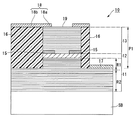
図1は、本発明の一実施形態による面発光型半導体レーザを模式的に示す断面図である。図1に示す通り、本実施形態の面発光型半導体レーザ10は、半導体基板(本実施形態ではn型GaAs基板)SB上に形成されている。この面発光型半導体レーザ10は垂直共振器を有しており、本実施形態では垂直共振器をなす一方の分布反射型多層膜ミラー(第2ミラー)13、活性層12、及び他方の分布反射型多層膜ミラー(第1ミラー)11の一部が柱状の半導体堆積体(以下、柱状部という)P1に形成されている。つまり、面発光型半導体レーザ10はその一部が柱状部P1に含まれた構造である。
[Surface emitting semiconductor laser]
FIG. 1 is a sectional view schematically showing a surface emitting semiconductor laser according to an embodiment of the present invention. As shown in FIG. 1, the surface-emitting
面発光型半導体レーザ10は、上記の第1ミラー11、活性層12、及び第2ミラー13が半導体基板SB上に順に積層された構造である。第1ミラー11及び第2ミラー13は、組成が異なる三元混晶半導体を交互に積層した分布反射型多層膜ミラーである。第1ミラーは、例えば、n型Al0.15Ga0.85As層(以下、低組成層という)とn型Al0.9Ga0.1As層(以下、高組成層という)とを交互に積層した25ペアの分布反射型多層膜ミラーである。詳細は後述するが、第1ミラー11の一部には低組成層と高組成層との間にAl組成をなだらかに変化させた組成傾斜層(GI層)が形成されている。
The surface emitting
尚、本実施形態において、低組成層とはAlGaAs層のガリウム(Ga)に対するアルミニウム(Al)の組成が低い層をいい、高組成層とはAlGaAs層のガリウム(Ga)に対するアルミニウム(Al)の組成が高い層をいう。AlGaAs層のAl組成は、「0」から「1」までである。即ち、AlGaAs層は、GaAs層(Al組成が「0」の場合)及びAlAs層(Al組成が「1」の場合)を含む。また、以上説明した第1ミラー11、活性層12、及び第2ミラー13を構成する各層の組成及び層数は特に限定される訳ではない。尚、第2ミラー13の最上層のAl組成は、0.3未満であることが好ましい。
In this embodiment, the low composition layer is a layer having a low composition of aluminum (Al) with respect to gallium (Ga) in the AlGaAs layer, and the high composition layer is a composition of aluminum (Al) with respect to gallium (Ga) in the AlGaAs layer. A layer having a high composition. The Al composition of the AlGaAs layer is from “0” to “1”. That is, the AlGaAs layer includes a GaAs layer (when the Al composition is “0”) and an AlAs layer (when the Al composition is “1”). The composition and the number of layers constituting the
活性層12は、第1ミラー11上に形成されており、GaAsウェル層とAl0.3Ga0.7Asバリア層からなり、ウェル層が3層で構成される量子井戸構造を含む構造である。第2ミラー13は、活性層12上に形成されており、p型Al0.15Ga0.85As層(以下、低組成層という)とp型Al0.9Ga0.1As層(以下、高組成層という)とを交互に積層した25ペアの分布反射型多層膜ミラーである。尚、第2ミラー13の最上層は、Al組成の小さい方、即ちp型Al0.15Ga0.85As層となるように構成されている。詳細は後述するが、第2ミラー13をなす低組成層と高組成層との間には、Al組成をなだらかに変化させた組成傾斜層(GI層)が形成されている。
The
面発光型半導体レーザ10をなす第1ミラー11は、例えばケイ素(Si)がドーピングされることによりn型にされており、第2ミラー13は、例えば炭素(C)がドーピングされることによりp型にされている。従って、p型の第2ミラー13、不純物がドーピングされていない活性層12、及びn型の第1ミラー11により、pinダイオードが形成される。
The
次に、第1ミラー11及び第2ミラー13について詳細に説明する。図2は、活性層12近傍の第1ミラー11及び第2ミラー13を拡大した断面図である。図2に示す通り、第1ミラー11は、活性層12に接する第1領域R1と、第1領域R1の下方に位置する第2領域R2とに大別される。第1領域R1は、低組成層L1と高組成層L2とが交互に積層されるとともに、低組成層L1と高組成層L2との間にAl組成をなだらかに変化させたGI層L3が形成された領域である。これに対し、第2領域R2は、低組成層L1と高組成層L2とが交互に積層された領域であり、第1領域R1のように低組成層L1と高組成層L2との間にGI層は形成されていない。
Next, the
また、第2ミラー13は第1ミラー11のように領域に区別されてはおらず、その全体に低組成層L4と高組成層L5とが交互に積層されるとともに、低組成層L4と高組成層L5との間にGI層L6が形成されている。即ち、第2ミラー13は、その全体が第1ミラー11の第1領域R1と似た構造である。ここで、第1ミラー11に形成される高組成層L1及び低組成層L2、並びに第2ミラー13に形成される高組成層L4及び低組成層L5の各々は、光学的膜厚がλ/4となるよう設定されている。尚、λは面発光型半導体レーザ10のレーザ光の波長である。
Further, the
第1ミラー11の第1領域R1及び第2ミラー13にそれぞれ形成されるGI層L3,L6は、例えば、Al組成を0.15〜0.9の間でなだらかに変化させたものであり、低組成層L1と高組成層L2との界面におけるエネルギー障壁及び低組成層L4と高組成層L5との界面におけるエネルギー障壁をなだらかにして抵抗を低減するために設けられる。Al組成が変化すると屈折率も変化するため、GI層L3,L6が形成された箇所においては、屈折率がなだらかに変化している。尚、図1,2に示す通り、面発光型半導体レーザ10を駆動するための電極17,18は、第1ミラー11の第1領域R1内における低組成層L1上、及び第2ミラー13上にそれぞれ形成されており、第1ミラー11の第2領域R2には電流が殆ど流れない。
The GI layers L3 and L6 respectively formed in the first region R1 and the
第1ミラー11の第1領域R1内におけるGI層L3は第1ミラー11の抵抗を低減するために設けられ、第2ミラー13のGI層L6は第2ミラー13の抵抗を低減するために設けられる。しかしながら、上述の通り、低組成層L1と高組成層L2との間にGI層L3を形成すると屈折率もなだらかに変化し、低組成層L4と高組成層L5との間にGI層L6を形成すると屈折率もなだらかに変化する。第1ミラー11を高い反射率にするためには、低組成層L1と高組成層L2との間で屈折率が急峻に変化する方が望ましい。このため、本実施形態では、電流が殆ど流れない第2領域R2内の低組成層L1と高組成層L2との間にはGI層を設けない構造とし、第1ミラー11の反射率を高めている。
The GI layer L3 in the first region R1 of the
ここで、第1ミラー11の最上層に形成された第1番目のペアから第5番目のペア程度までのペアが第1領域R1に含まれるようにするのが望ましい。面発光型半導体レーザ10の抵抗低減のためには、電極17が接触している低組成層L1が活性層12に極力近いことが好ましい。しかしながら、前述した通り、本実施形態の面発光型半導体レーザ10はその一部が柱状部P1に含まれた構造であるため、その柱状部P1の根本部分に応力が集中しやすく、この根本部分が劣化しやすい。
Here, it is desirable that the first region R1 includes the first to fifth pairs formed in the uppermost layer of the
図1及び図2に示す通り、柱状部P1の根本部分には電極17が接触する低組成層L1が配置されており、この低組成層L1と活性層12とが近すぎると面発光型半導体レーザ10の特性の劣化を招きやすい。逆に、活性層12から余りにも離れた位置に電極17が接触する低組成層L1(又は高組成層L2)を形成すると、上述したGI層L3が形成されているとはいっても、抵抗が高くなってしまう。よって、第1ミラー11の最上層に形成された第1番目のペアから第5番目のペア程度までのペアが第1領域R1に含まれるようにすることで、抵抗を低減しつつ上記の劣化も防止することができる。
As shown in FIGS. 1 and 2, a low composition layer L1 in contact with the
ここで、GI層を形成した場合及び形成しない場合の反射率の変化について説明する。図3は、GI層の有無による変化率の変化を説明するための図である。尚、図3においては、横軸に波長を取り、縦軸に反射率を取っている。図3おいて、符号G1を付して示す点線の曲線は、低組成層と高組成層とのペア数が25ペアであり、GI層が形成されていない場合の波長に対する反射率の変化を示している。 Here, the change in reflectance when the GI layer is formed and when it is not formed will be described. FIG. 3 is a diagram for explaining the change in the change rate depending on the presence or absence of the GI layer. In FIG. 3, the horizontal axis represents wavelength and the vertical axis represents reflectance. In FIG. 3, the dotted curve indicated by reference numeral G1 shows the change in reflectance with respect to the wavelength when the number of pairs of the low composition layer and the high composition layer is 25 and the GI layer is not formed. Show.
また、符号G2を付して示す破線の曲線は、低組成層と高組成層とのペア数が25ペアであり、低組成層と高組成層との間にGI層が形成されている場合の波長に対する反射率の変化を示している。更に、符号G3を付して示す実線の曲線は、低組成層と高組成層とのペア数が25ペアであり、5ペア分の低組成層と高組成層との間にGI層が形成されている場合の波長に対する反射率の変化を示している。即ち、曲線G2は第2ミラー13の波長に対する反射率の変化を示しており、曲線G3は第1ミラー11の波長に対する反射率の変化を示している。
A broken line curve indicated by reference numeral G2 indicates that the number of pairs of the low composition layer and the high composition layer is 25, and a GI layer is formed between the low composition layer and the high composition layer. The change of the reflectance with respect to the wavelength of is shown. Furthermore, the solid curve indicated by reference numeral G3 indicates that the number of pairs of the low composition layer and the high composition layer is 25, and a GI layer is formed between the low composition layer and the high composition layer for 5 pairs. The change of the reflectance with respect to the wavelength in the case of being performed is shown. That is, the curve G2 indicates the change in reflectance with respect to the wavelength of the
曲線G1と曲線G2とを比較すると、25ペア分の低組成層と高組成層との間にGI層を形成した場合にはGI層を全く形成しない場合に比べて反射率が低下するとともに、高い反射率(99.9%程度)が得られる波長領域が狭くなることが分かる。反射率が低下すると面発光型半導体レーザ10の発振閾値が上昇する虞がある。また、高反射率が得られる波長領域が狭くなると、面発光型半導体レーザ10の設計マージンが狭くなって歩留まりの低下を招く可能性がある。
Comparing the curve G1 and the curve G2, when the GI layer is formed between the low composition layer and the high composition layer for 25 pairs, the reflectance is lower than the case where the GI layer is not formed at all. It can be seen that the wavelength region where high reflectivity (about 99.9%) can be obtained becomes narrow. When the reflectance is lowered, the oscillation threshold value of the surface emitting
次に、曲線G3に着目すると、25ペアのうちの5ペア分の低組成層と高組成層との間のみにGI層を形成した場合にはGI層を全く形成しない場合に比べて若干反射率が低下するものの、GI層を全く形成しない場合とほぼ同様の反射率が得られている。また、曲線G3の高反射率が得られる波長領域は、曲線G1のそれとほぼ同様である。前述した通り、柱状部P1の根本部分の応力集中に加えて、以上の反射率の変化も考慮すると、第1ミラー11の最上層に形成された第1番目のペアから第5番目の程度までのペアが第1領域R1に含まれるようにするのが望ましい。
Next, paying attention to the curve G3, when the GI layer is formed only between the low composition layer and the high composition layer for 5 pairs out of 25 pairs, it is slightly reflected as compared with the case where the GI layer is not formed at all. Although the rate decreases, a reflectance almost similar to that obtained when no GI layer is formed is obtained. The wavelength region where the high reflectance of the curve G3 is obtained is almost the same as that of the curve G1. As described above, in addition to the stress concentration at the base portion of the columnar part P1, the above change in reflectance is also taken into consideration, from the first pair formed in the uppermost layer of the
図1に戻り、面発光型半導体レーザ10のうち、第2ミラー13から第1ミラー11の第1領域R1内の途中までの部分が、第2ミラー13の上面からみて円形の形状にエッチングされて柱状部P1が形成されている。尚、本実施形態では、柱状部P1の平面形状が円形である場合を例に挙げて説明するが、この形状は任意の形状とすることができる。
Returning to FIG. 1, in the surface emitting
更に、第2ミラー13を構成する層のうち活性層12に近い領域に、AlGaAs層を側面から酸化することにより得られる電流狭窄層15が形成されている。この電流狭窄層15はリング状に形成されている。即ち、この電流狭窄層15は、半導体基板SBの表面と平行な面で切断した場合における断面形状が、柱状部P1の平面形状の円形と同心の円のリング状である。
Further, a
また、本実施形態の面発光型半導体レーザ10は、柱状部P1の周囲を取り囲むよう第1ミラー11(柱状部P1の周囲に露出している低組成層L1上に絶縁層16が形成されている。第1柱状部P1の周囲を絶縁層16で取り込むことで、柱状部P1をなす各層の酸化等が防止されるため、面発光型半導体レーザ10の信頼性を高めることができる。絶縁層16は、その膜厚が例えば2〜4μm程度であり、熱又は光等のエネルギーによって硬化可能な液体材料(例えば紫外線硬化型樹脂や熱硬化型樹脂の前駆体)を硬化させることにより得られるものを用いることができる。紫外線硬化型樹脂としては、例えば紫外線硬化型のアクリル系樹脂及びエポキシ系樹脂が挙げられる。また、熱硬化型樹脂としては、熱硬化型のポリイミド系樹脂等が例示できる。
Further, in the surface emitting
また、第1ミラー11(柱状部P1の周囲に露出している低組成層L1)上には電極17が形成されており、第2ミラー13上には電極18が形成されている。電極17は、第1ミラー11の上面(柱状部P1の周囲に露出している低組成層L1)に接合されて電気的に接続されている。尚、この電極は不図示のパッド部に接続されている。また、本実施形態では、柱状部P1の周囲に露出している低組成層L1上に電極17が形成されている場合を例に挙げて説明するが柱状部P1の周囲に高組成層L2が露出している場合には、この高組成層L2上に電極17を形成しても良い。
An
電極18は、例えば第2ミラー13の中央部を開口する平面形状がリング状の接続部18aと、この接続部18aと不図示のパッド部(上記の電極17が接続されるパッド部とは異なるパッド部)とを接続する引き出し部18bとを有している。接続部18aは第2ミラー13の上面に接合されて電気的に接続されている。尚、第2ミラー13の上面はレーザ光の射出面19とされている。引き出し部18bは、絶縁層16上に形成されており、不図示のパッド部まで延びている。
The
電極17は、例えば金(Au)とゲルマニウム(Ge)の合金と、金(Au)との積層膜からなり、柱状部P1の周囲に露出している低組成層L1とオーミックコンタクトが取られている。また、電極18は、例えば白金(Pt)、チタン(Ti)及び金(Au)の積層膜からなり、第2ミラー13の上面とオーミックコンタクトが取られている。これら電極17,18は、面発光型半導体レーザ10を駆動するためのものであり、電極17と電極18とによって活性層12に電流が注入される。尚、電極17及び電極18を形成するための材料は、前述したものに限定される訳ではなく、例えば金(Au)と亜鉛(Zn)との合金等が利用可能である。
The
次に、本実施形態の面発光型半導体レーザ10の一般的な動作について説明する。尚、下記の面発光型半導体レーザ10の駆動方法は一例であり、本発明の範囲内で種々の変更が可能である。まず、電極17と電極18とを不図示の電源に接続してpinダイオードに順方向の電圧を印加すると、電極18から第2ミラー13を介して活性層12に正孔が流れ込むとともに、電極17から第1ミラー11の第1領域R1に含まれる低組成層L1を介して電子が流れ込む。面発光型半導体レーザ10の活性層12において、電子と正孔との再結合が生じ、再結合による発光が生じる。そこで生じた光が第2ミラー13と第1ミラー11との間を往復する間に誘導放出が起こって光の強度が増幅される。光利得が光損失を上まわると、レーザ発振が起こり、第2ミラー13の上面(射出面19)からレーザ光が射出される。
Next, a general operation of the surface emitting
〔面発光型半導体レーザの製造方法〕
次に、以上説明した面発光型半導体レーザ10の製造方法について説明する。図4〜図6は、本発明の一実施形態による面発光型半導体レーザの製造工程を模式的に示す断面図である。尚、これらの図は図1に示す断面図に対応している。本実施形態の面発光型半導体レーザ10を製造するには、図4(a)に示す通り、まずn型GaAs層からなる半導体基板SBの表面に組成を変調させながらエピタキシャル成長させて半導体多層膜を形成する。
[Method of manufacturing surface emitting semiconductor laser]
Next, a manufacturing method of the surface emitting
ここで、半導体多層膜は、第ミラー11、活性層12、及び第2ミラー13からなる。第1ミラー11を形成するには、例えばn型Al0.15Ga0.85As層(低組成層L1)とn型Al0.9Ga0.1As層(高組成層L2)とを交互に積層して20ペア程度形成して第2領域R2を形成する。尚、低組成層L1及び高組成層L2は、その光学的膜厚がλ/4となるよう形成する。次に、積層された低組成層L1及び高組成層L2からなる第2領域R2上に第1領域R1を形成する。具体的には、低組成層L1、GI層L3、及び高組成層L2を順に積層して5ペア程度形成する。尚、第1領域R1の低組成層L1及び高組成層L2も、その光学的膜厚がλ/4となるよう形成する。
Here, the semiconductor multilayer film includes the
活性層12は、例えばGaAsウェル層とAl0.3Ga0.7Asバリア層とからなり、ウェル層が3層で構成される量子井戸構造とする。第2ミラー13は、p型Al0.15Ga0.85As層(低組成層L4)、GI層L6、及びp型Al0.9Ga0.1As層(高組成層L5)を順に積層して25ペア程度形成する。第2ミラー13をなすこれら低組成層L4及び高組成層L5も、その光学的膜厚がλ/4となるよう形成する。尚、第2ミラー13の最上層は、低組成層L4とする。
The
尚、第2ミラー13を成長させる際に、活性層12近傍の少なくとも1層は、後に酸化されて電流狭窄層15となる層に形成される(図5(a)参照)。このため、電流狭窄層15となる層は、Al組成がより大きなAlGaAs層(AlAs層を含む)に形成される。例えば、例えば電流狭窄層15となる層は、Al組成が0.95以上となるように形成するのが望ましい。
When the
また、後の工程において電極18が形成された際に、第2ミラー13のうち少なくとも電極18と接する部分は、キャリア密度を高くすることにより、電極18とのオーム性接触をとり易くし、且つ電極18との密着性を高められるようにするのが望ましい。同様に、第2ミラー11の第1領域R1に含まれる低組成層L1のうち、後に電極17と接する低組成層L1は、他の低組成層L1よりもキャリア密度を高くすることにより、電極17とのオーム性接触をとり易くし、且つ電極17との密着性を高められるようにするのが望ましい。
In addition, when the
エピタキシャル成長を行う際の温度は、成長方法や原料、半導体基板SBの種類、或いは形成する半導体多層膜の種類、厚さ、及びキャリア密度によって適宜決定されるが、一般に、450℃〜800℃に設定するのが好ましい。また、エピタキシャル成長を行う際の所要時間も、温度と同様に適宜決定される。また、エピタキシャル成長させる方法としては、有機金属気相成長(MOVPE:Metal-Organic Vapor Phase Epitaxy)法、MBE(Molecular Beam Epitaxy)法、或いはLPE(Liquid Phase Epitaxy)法を用いることができる。 The temperature at which the epitaxial growth is performed is appropriately determined depending on the growth method, the raw material, the type of the semiconductor substrate SB, or the type, thickness, and carrier density of the semiconductor multilayer film to be formed, but is generally set to 450 ° C. to 800 ° C. It is preferable to do this. Further, the time required for performing the epitaxial growth is also appropriately determined in the same manner as the temperature. As a method for epitaxial growth, a metal-organic vapor phase epitaxy (MOVPE) method, a molecular beam epitaxy (MBE) method, or a liquid phase epitaxy (LPE) method can be used.
次に、図4(b)に示す通り、柱状部P1を形成する。柱状部P1を形成するには、まず、半導体多層膜上にレジスト(図示省略)を塗布した後、リソグラフィ法によりレジストをパターニングする。これにより、第2ミラー13の上面に所定の平面形状を有するレジスト層が形成される。次いで、このレジスト層をマスクとして、例えばドライエッチング法により、第2ミラー13、活性層12、及び第1ミラー11の第1領域R1の内部までエッチングする。具体的には、第1領域R1に含まれる低組成層L1のうち、他の低組成層L1よりもキャリア密度を高くした低組成層L1の上部に位置する高組成層L2(図2参照)までエッチングする。
Next, as shown in FIG. 4B, the columnar portion P1 is formed. In order to form the columnar portion P1, first, a resist (not shown) is applied on the semiconductor multilayer film, and then the resist is patterned by a lithography method. As a result, a resist layer having a predetermined planar shape is formed on the upper surface of the
ドライエッチング法によりエッチングを行っている最中は、プラズマ中に含まれるアルミニウム(Al)及びガリウム(Ga)の少なくとも一方に起因する発光スペクトルの強度をモニタする。そして、このモニタ結果に基づいてエッチング量を制御する。これにより、第2ミラー13、活性層12、及び第1ミラー11の上部が同一の平面形状にされた柱状部P1が形成される。尚、柱状部P1が形成されると、レジスト層は除去される。
During etching by the dry etching method, the intensity of the emission spectrum caused by at least one of aluminum (Al) and gallium (Ga) contained in the plasma is monitored. Then, the etching amount is controlled based on the monitoring result. Thereby, the columnar part P1 in which the upper part of the
柱状部P1が形成されると、図5(a)に示す通り、電流狭窄層15が形成される。この電流狭窄層15を形成するには、上記工程によって柱状部P1が形成された半導体基板SBを、例えば400℃程度の水蒸気雰囲気中に投入する。これにより、前述した第2ミラー13中のAl組成が高い層が側面から酸化されて、電流狭窄層15が形成される。
When the columnar portion P1 is formed, the
酸化レートは、炉の温度、水蒸気の供給量、酸化すべき層のAl組成、及び膜厚に依存する。酸化により形成される電流狭窄層15を備えた面発光型半導体レーザでは、駆動する際に、電流狭窄層15が形成されていない部分(酸化されていない部分)のみに電流が流れる。従って、電流狭窄層15を形成する工程において、形成する電流狭窄層15の範囲を制御することにより、電流密度の制御が可能となる。
The oxidation rate depends on the furnace temperature, the amount of steam supplied, the Al composition of the layer to be oxidized, and the film thickness. In the surface emitting semiconductor laser including the
次に、図5(b)に示す通り、柱状部P1の周囲に露出している低組成層L1上に絶縁層16を形成する。この絶縁層16は、厚膜化が容易なものを用いることが望ましい。絶縁層16の膜厚は、例えば2〜4μm程度であるが、特に限定される訳ではない。例えば、絶縁層16は、熱又は光等のエネルギーによって硬化可能な液体材料(例えば紫外線硬化型樹脂や熱硬化型樹脂の前駆体)を硬化させることにより得られるものを用いることができる。紫外線硬化型樹脂としては、例えば紫外線硬化型のアクリル系樹脂及びエポキシ系樹脂が挙げられる。また、熱硬化型樹脂としては、熱硬化型のポリイミド系樹脂等が例示できる。また、例えば、絶縁層16は、上記材料を複数用いて積層膜とすることもできる。
Next, as shown in FIG. 5B, the insulating
ここでは、絶縁層16を形成するための材料として、ポリイミド系樹脂の前駆体を用いた場合について述べる。まず、例えばスピンコート法を用いて前駆体(ポリイミド系樹脂の前駆体)を第1ミラー11(柱状部P1の周囲に露出している低組成層L1)上に塗布して前駆体層を形成する。尚、前駆体層の形成方法としては、前述したスピンコート法のほか、ディッピング法、スプレーコート法、液滴吐出法等の公知技術が利用できる。次いで、例えばホットプレート等を用いて半導体基板SBを加熱して溶媒を除去した後、例えば350℃程度の炉に入れて前駆体層をイミド化させることにより、ほぼ完全に硬化したポリイミド系樹脂層を形成する。続いて、ポリイミド系樹脂層を公知のリソグラフィ技術を用いてパターニングすることにより絶縁層16を形成する。
Here, a case where a polyimide resin precursor is used as a material for forming the insulating
尚、パターニングの際に用いられるエッチング方法としては、ドライエッチング法等を用いることができる。ドライエッチングは、例えば酸素又はアルゴン等のプラズマにより行うことができる。また、上述の絶縁層16の形成方法では、ポリイミド系樹脂の前駆体層を硬化した後、パターニングを行う例について示したが、ポリイミド系樹脂の前駆体層を硬化する前に、パターニングを行うこともできる。このパターニングの際に用いられるエッチング方法としては、ウェットエッチング法等を用いることができる。ウェットエッチングは、例えばアルカリ溶液又は有機溶液等により行うことができる。
As an etching method used for patterning, a dry etching method or the like can be used. Dry etching can be performed by plasma such as oxygen or argon. In the above-described method for forming the insulating
以上の工程が終了すると、図6に示す通り、第1ミラー11(柱状部P1の周囲に露出している低組成層L1)の上面上に電極17が形成され、第2ミラー13の上面上に電極18が形成される。尚、前述した通り、電極18は、リング状の平面形状を有する接続部18a及び直線状の平面形状を有する引き出し部18bを有しているが、第2ミラー13の上面上には接続部18aが形成され、引き出し部18bは絶縁層16上に形成される。
When the above steps are completed, an
電極18を形成する具体的な方法は以下の通りである。まず、電極18を形成する前に、必要に応じてプラズマ処理法等を用いて、第2ミラー13の上面を洗浄する。これにより、より安定した特性の素子を形成することができる。次に、例えば真空蒸着法により、例えば白金(Pt)、チタン(Ti)、及び金(Au)の積層膜(図示省略)を形成する。次いで、リフトオフ法により、所定の位置以外の積層膜を除去することにより電極18が形成される。
A specific method for forming the
この際、第2ミラー13の上面に、積層膜が形成されていない部分が形成される。この部分が開口部となり、この開口部によって第2ミラー13の上面の一部が露出する。この露出した面がレーザ光の射出面19となる。尚、上記工程において、リフトオフ法の代わりにドライエッチング法又はウェットエッチング法を用いることもできる。また、上記工程において、真空蒸着法の代わりにスパッタ法を用いることもできる。
At this time, a portion where the laminated film is not formed is formed on the upper surface of the
次に、電極18を形成する場合と同様の方法で、例えば金(Au)とゲルマニウム(Ge)の合金と金(Au)との積層膜をパターニングすることで、図6に示す通り、第1ミラー11(柱状部P1の周囲に露出している低組成層L1)上に電極17を形成する。最後に、アニール処理を行う。アニール処理の温度は電極材料に依存する。本実施形態で用いる電極材料の場合は、通常400℃前後で行う。以上の工程により、電極17,18が形成される。以上の工程によって図1に示す本実施形態の面発光型半導体レーザ10が製造される。
Next, by patterning a laminated film of, for example, an alloy of gold (Au) and germanium (Ge) and gold (Au) by the same method as in the case of forming the
以上説明した通り、本実施形態の面発光型半導体レーザ10は、第1ミラー11の活性層12に接する第1領域R1内に積層された低組成層L1と高組成層L2との間にGI層L3が形成されており、第2ミラー13、活性層12、及び第1ミラー11の第1領域R1の内部までエッチングされて柱状部P1が形成されている。また、第2ミラー13は、低組成層L4と高組成層L5との間にGI層L6が形成されている。更に、エッチングによって露出した第1ミラー11(柱状部P1の周囲に露出している低組成層L1)上に電極17が形成され、第2ミラー13上に電極18が形成されている。よって、電極17,18を介する電流の流路上には積層された異なる種類の半導体層の界面におけるエネルギー障壁が殆ど存在しないため、面発光型半導体レーザ10の抵抗を低減することができる。
As described above, the surface emitting
また、第1ミラー11の第2領域R2には、低組成層L1と高組成層L2とが交互に積層されており、第1領域R1のように低組成層L1と高組成層L2との間にGI層L3は形成されていない。よって、低組成層L1と高組成層L2との間では、屈折率が急峻に変化している。このため、本実施形態では、電流が殆ど流れない第2領域R2は反射率を高めることができ、第1ミラー11の第1領域R1にGI層L3を形成したことによる反射率の大幅な低下を防止することができる。この結果として、面発光型半導体レーザ10の発振閾値の上昇を抑えることができる。
In addition, the low composition layer L1 and the high composition layer L2 are alternately stacked in the second region R2 of the
〔他の実施形態〕
次に、本発明の他の実施形態について説明する。図7は、本発明の他の実施形態による面発光型半導体レーザを模式的に示す断面図である。尚、図7においては、図1に示す部材と同一の部材については同一の符号を付してある。図7に示す通り、本実施形態の面発光型半導体レーザ20は、半導体基板(本実施形態ではn型GaAs基板)SB上に形成されており、第1ミラー11、活性層12、及び第2ミラー23を含んで構成される。
[Other Embodiments]
Next, another embodiment of the present invention will be described. FIG. 7 is a cross-sectional view schematically showing a surface emitting semiconductor laser according to another embodiment of the present invention. In FIG. 7, the same members as those shown in FIG. 1 are denoted by the same reference numerals. As shown in FIG. 7, the surface emitting semiconductor laser 20 of the present embodiment is formed on a semiconductor substrate (n-type GaAs substrate in this embodiment) SB, and includes a
図7に示す通り、本実施形態の面発光型半導体レーザ20が備える第1ミラー11は、図1に示す面発光型半導体レーザ10が備えるものと同じである。即ち、活性層12に接する第1領域R1と、第1領域R1の下方に位置する第2領域R2とに大別され、第1領域R1には低組成層L1と高組成層L2とが交互に積層されるとともに、低組成層L1と高組成層L2との間にAl組成をなだらかに変化させたGI層L3が形成されており、第2領域R2には低組成層L1と高組成層L2とが交互に積層されている。また、本実施形態の面発光型半導体レーザ20が備える活性層12は、図1に示す面発光型半導体レーザ10が備えるものと同じである。
As shown in FIG. 7, the
本実施形態の面発光型半導体レーザ20は、活性層12上に形成されるミラー(第2ミラー23)の構造が図1に示す面発光型半導体レーザ10が備える第2ミラー13とは異なる。本実施形態の面発光型半導体レーザ20が備える第2ミラー23は、活性層12に接する第4領域R4と、第4領域R4の上方に位置する第3領域R4とに大別される。第4領域R4は、低組成層L4と高組成層L5とが交互に積層されるとともに、低組成層L4と高組成層L5との間にAl組成をなだらかに変化させたGI層L6が形成された領域である。即ち、第4領域R4には、図1に示す第2ミラー13と同じ構造のミラーが形成されている。
The surface emitting semiconductor laser 20 of the present embodiment is different from the
これに対し、第3領域R3には誘電体多層膜からなるミラーが形成されている。上記の通り、第2ミラー23の第4領域R4には低組成層L4と高組成層L5との間にGI層L6が形成されているため、第2ミラー23の反射率が低下する。このため、この反射率の低下を補うために第3領域R3に誘電体多層膜からなるミラーを形成している。第3領域R3に形成されるミラーは、例えばSiO2とTiO2とからなる誘電体多層膜であり、そのペア数は第2ミラー23で必要となる反射率に応じて決定される。
On the other hand, a mirror made of a dielectric multilayer film is formed in the third region R3. As described above, since the GI layer L6 is formed between the low composition layer L4 and the high composition layer L5 in the fourth region R4 of the
また、図7に示す通り、第2ミラー23の第3領域R3は、柱状部P1よりも径が小さな柱状形状に形成されている。第3領域R3の周囲には、電極18が形成されているため、本実施形態の面発光型半導体レーザ20は、図1に示す面発光型半導体レーザ10のレーザ光の射出面19上に誘電体多層膜からなるミラー(第3領域R3)を形成したものであるということもできる。以上の構造を有する本実施形態の面発光型半導体レーザ20は、図1に示す面発光型半導体レーザ10に比べて第2ミラー23の反射率を高めることができるため、発振閾値の上昇を更に抑えることができる。
Further, as shown in FIG. 7, the third region R3 of the
以上、本発明の実施形態について説明したが、本発明は上記の実施形態に限定されることはなく、本発明の範囲内で自由に変更が可能である。例えば、図1に示す面発光型半導体レーザ10では、第1ミラー11についてのみ第1領域R1と第2領域R2とに分け、活性層12に接する第1領域R1には低組成層L1と、高組成層L2と、低組成層L1と高組成層L2との間のGI層L3とを積層し、第2領域R2には低組成層L1と高組成層L2とを積層していた。
As mentioned above, although embodiment of this invention was described, this invention is not limited to said embodiment, It can change freely within the scope of the present invention. For example, in the surface-emitting
また、図7に示す面発光型半導体レーザ20では、図1に示す面発光型半導体レーザ10と同様に第1ミラー11については第1領域R1と第2領域R2とに分けている。一方、第2ミラー23については、第3領域R3と第4領域R4とに分け、活性層12に接する第4領域R4には低組成層L4と、高組成層L5と、低組成層L4と高組成層L5との間のGI層L6とを積層し、第3領域R3には誘電体多層膜を形成していた。
In the surface emitting semiconductor laser 20 shown in FIG. 7, the
しかしながら、上記の例の如く2つの領域に分けるのは、第2ミラー13についてのみであっても良い。第2ミラー13についてのみ上記の2領域を形成する場合には、活性層12に接する領域に低組成層L4と、高組成層L5と、低組成層L4と高組成層L5との間のGI層L6とを積層し、この領域の上部に位置する領域には低組成層L4と高組成層L5とを積層した構造とする。
However, only the
かかる構造の場合には、第2ミラー13のみを柱状形状としてGI層L6が形成された領域の低組成層L4(又は、高組成層L5)に電極18に相当する電極を接続することが好適である。また、かかる構造の場合には、第1ミラー11の全体を低組成層L1と、高組成層L2と、低組成層L1と高組成層L2との間のGI層L3とを積層した構造とし、電極17に相当する電極を第1ミラー11の底面(基板SBを除去することにより露出した第1ミラー11の底面)に接続するのが好適である。
In the case of such a structure, it is preferable to connect the electrode corresponding to the
更に、かかる構造の場合には、基板SBを除去することにより露出した第1ミラー11の底面であって、柱状部P1の下方の位置に、図7に示す第2ミラー23の第3領域R3に形成される誘電体多層膜からなるミラーと同様のミラーを形成するのが好ましい。かかるミラーを形成することで第1ミラー11の反射率の低下を防止することができる。
Further, in the case of such a structure, the third region R3 of the
また、上記実施形態においてはAl組成が異なるAlGaAs層を用いて第1ミラー11及び第2ミラー13を形成していたが、本発明はAlGaAs層に限られる訳ではなく、他の半導体層を用いて第1ミラー11及び第2ミラー13が形成されている面発光型半導体レーザにも適用可能である。更に、上記実施形態において、各半導体層におけるp型とn型とを入れ替えても本発明の範囲外となるものではない。
Moreover, in the said embodiment, although the
更に、上記実施形態で説明した面発光型半導体レーザ10は柱状部P1が形成された構造であったが、本発明の面発光型半導体レーザは必ずしもこの構造にする必要はない。例えば、レーザ光の射出面の周囲数カ所に、第2ミラー13から第1ミラー11の上部に至る孔が形成された構造であっても良い。尚、この孔は電流狭窄層を形成するために用いられる孔である。
Furthermore, although the surface emitting
10……面発光型半導体レーザ
11……第1ミラー
12……活性層
13……第2ミラー
17,18……電極
20……面発光型半導体レーザ
23……第2ミラー
L1……低組成層
L2……高組成層
L3……GI層
P1……柱状部
R1……第1領域
R2……第2領域
R3……第3領域
DESCRIPTION OF
Claims (15)
前記上部ミラー及び前記下部ミラーの少なくとも一方は、前記活性層に接する領域であって、第1屈折率を有する第1半導体層と、第2屈折率を有する第2半導体層と、前記第1半導体層と前記第2半導体層との間に前記第1屈折率と前記第2屈折率との間の屈折率を有する第3半導体層とが形成された第1領域と、
前記第1半導体層と前記第2半導体層とが交互に積層されてなる第2領域と
を備えることを特徴とする面発光型半導体レーザ。 A surface emission that includes an upper mirror and a lower mirror, and an active layer disposed between the upper mirror and the lower mirror, and emits laser light in the stacking direction of the lower mirror, the active layer, and the upper mirror Type semiconductor laser
At least one of the upper mirror and the lower mirror is a region in contact with the active layer, and includes a first semiconductor layer having a first refractive index, a second semiconductor layer having a second refractive index, and the first semiconductor. A first region in which a third semiconductor layer having a refractive index between the first refractive index and the second refractive index is formed between a layer and the second semiconductor layer;
A surface-emitting semiconductor laser comprising: a second region in which the first semiconductor layer and the second semiconductor layer are alternately stacked.
前記第3半導体層は、前記第1半導体層及び前記第2半導体層の間の各々に形成されている
ことを特徴とする請求項1記載の面発光型半導体レーザ。 A plurality of the first semiconductor layer and the second semiconductor layer are formed in the first region;
The surface emitting semiconductor laser according to claim 1, wherein the third semiconductor layer is formed between each of the first semiconductor layer and the second semiconductor layer.
前記下部ミラーが備える前記第1領域に対して設けられる第2電極と
を含むことを特徴とする請求項4又は請求項5記載の面発光型半導体レーザ。 The electrode includes a first electrode provided for the first region of the upper mirror;
The surface emitting semiconductor laser according to claim 4, further comprising: a second electrode provided for the first region of the lower mirror.
前記上部ミラー及び前記下部ミラーを形成する際に、
前記上部ミラー及び前記下部ミラーの少なくとも一方に、第1屈折率を有する第1半導体層と、第2屈折率を有する第2半導体層と、前記第1半導体層と前記第2半導体層との間に前記第1屈折率と前記第2屈折率との間の屈折率を有する第3半導体層とを含んで前記活性層に接する第1領域を形成する工程と、
前記第1半導体層と前記第2半導体層とが交互に積層されてなる第2領域を前記第1領域以外の領域に形成する工程と
を含むことを特徴とする面発光型半導体レーザの製造方法。 A surface emission that includes an upper mirror and a lower mirror, and an active layer disposed between the upper mirror and the lower mirror, and emits laser light in the stacking direction of the lower mirror, the active layer, and the upper mirror Type semiconductor laser manufacturing method,
When forming the upper mirror and the lower mirror,
At least one of the upper mirror and the lower mirror includes a first semiconductor layer having a first refractive index, a second semiconductor layer having a second refractive index, and between the first semiconductor layer and the second semiconductor layer. Forming a first region in contact with the active layer including a third semiconductor layer having a refractive index between the first refractive index and the second refractive index;
Forming a second region formed by alternately laminating the first semiconductor layer and the second semiconductor layer in a region other than the first region. .
前記上部ミラー、前記活性層、及び前記下部ミラーに形成された前記第1領域の内部までエッチングする際に、前記組成の変化をモニタしつつエッチング量を制御することを特徴とする請求項14記載の面発光型半導体レーザの製造方法。
The first semiconductor layer and the second semiconductor layer are composed of mixed crystal semiconductors having different compositions,
15. The etching amount is controlled while monitoring the change in the composition when etching into the first region formed in the upper mirror, the active layer, and the lower mirror. Manufacturing method of the surface emitting semiconductor laser.
Priority Applications (2)
| Application Number | Priority Date | Filing Date | Title |
|---|---|---|---|
| JP2005358569A JP2007165501A (en) | 2005-12-13 | 2005-12-13 | Surface emitting semiconductor laser and manufacturing method thereof |
| US11/567,428 US20070133641A1 (en) | 2005-12-13 | 2006-12-06 | Surface-emitting type semiconductor laser and method for manufacturing the same |
Applications Claiming Priority (1)
| Application Number | Priority Date | Filing Date | Title |
|---|---|---|---|
| JP2005358569A JP2007165501A (en) | 2005-12-13 | 2005-12-13 | Surface emitting semiconductor laser and manufacturing method thereof |
Publications (1)
| Publication Number | Publication Date |
|---|---|
| JP2007165501A true JP2007165501A (en) | 2007-06-28 |
Family
ID=38179871
Family Applications (1)
| Application Number | Title | Priority Date | Filing Date |
|---|---|---|---|
| JP2005358569A Withdrawn JP2007165501A (en) | 2005-12-13 | 2005-12-13 | Surface emitting semiconductor laser and manufacturing method thereof |
Country Status (2)
| Country | Link |
|---|---|
| US (1) | US20070133641A1 (en) |
| JP (1) | JP2007165501A (en) |
Cited By (2)
| Publication number | Priority date | Publication date | Assignee | Title |
|---|---|---|---|---|
| EP2892116A2 (en) | 2013-12-20 | 2015-07-08 | Seiko Epson Corporation | Vertical cavity surface emitting laser and atomic oscillator |
| JP2018098347A (en) * | 2016-12-13 | 2018-06-21 | 学校法人 名城大学 | Semiconductor multilayer film-reflecting mirror, vertical resonator type light-emitting element using the same, and manufacturing methods thereof |
Families Citing this family (2)
| Publication number | Priority date | Publication date | Assignee | Title |
|---|---|---|---|---|
| TWI344709B (en) * | 2007-06-14 | 2011-07-01 | Epistar Corp | Light emitting device |
| US10698158B1 (en) * | 2017-11-28 | 2020-06-30 | Facebook Technologies, Llc | Optical waveguides in micro-LED devices |
Family Cites Families (11)
| Publication number | Priority date | Publication date | Assignee | Title |
|---|---|---|---|---|
| US5351256A (en) * | 1993-04-28 | 1994-09-27 | The United States Of America As Represented By The United States Department Of Energy | Electrically injected visible vertical cavity surface emitting laser diodes |
| US6542527B1 (en) * | 1998-08-27 | 2003-04-01 | Regents Of The University Of Minnesota | Vertical cavity surface emitting laser |
| US6362074B2 (en) * | 1998-12-29 | 2002-03-26 | Intel Corporation | Integrated circuit processing with improved gate electrode fabrication |
| US6727520B2 (en) * | 2000-12-29 | 2004-04-27 | Honeywell International Inc. | Spatially modulated reflector for an optoelectronic device |
| US20020126720A1 (en) * | 2001-03-07 | 2002-09-12 | Ying-Jay Yang | Device structure and method for fabricating semiconductor lasers |
| US6567454B1 (en) * | 2001-05-01 | 2003-05-20 | Sandia Corporation | Coupled-resonator vertical-cavity lasers with two active gain regions |
| JP2003133640A (en) * | 2001-08-10 | 2003-05-09 | Furukawa Electric Co Ltd:The | Surface light-emitting semiconductor laser element |
| US6711195B2 (en) * | 2002-02-28 | 2004-03-23 | Agilent Technologies, Inc. | Long-wavelength photonic device with GaAsSb quantum-well layer |
| WO2004006393A2 (en) * | 2002-07-06 | 2004-01-15 | Optical Communication Products, Inc. | Method of self-aligning an oxide aperture with an annular intra-cavity contact in a long wavelength vcsel |
| JP3885677B2 (en) * | 2002-07-10 | 2007-02-21 | 富士ゼロックス株式会社 | Surface emitting semiconductor laser, method for manufacturing the same, and apparatus for manufacturing the same |
| US7085301B2 (en) * | 2002-07-12 | 2006-08-01 | The Board Of Trustees Of The University Of Illinois | Photonic crystal single transverse mode defect structure for vertical cavity surface emitting laser |
-
2005
- 2005-12-13 JP JP2005358569A patent/JP2007165501A/en not_active Withdrawn
-
2006
- 2006-12-06 US US11/567,428 patent/US20070133641A1/en not_active Abandoned
Cited By (3)
| Publication number | Priority date | Publication date | Assignee | Title |
|---|---|---|---|---|
| EP2892116A2 (en) | 2013-12-20 | 2015-07-08 | Seiko Epson Corporation | Vertical cavity surface emitting laser and atomic oscillator |
| US9197034B2 (en) | 2013-12-20 | 2015-11-24 | Seiko Epson Corporation | Vertical cavity surface emitting laser and atomic oscillator |
| JP2018098347A (en) * | 2016-12-13 | 2018-06-21 | 学校法人 名城大学 | Semiconductor multilayer film-reflecting mirror, vertical resonator type light-emitting element using the same, and manufacturing methods thereof |
Also Published As
| Publication number | Publication date |
|---|---|
| US20070133641A1 (en) | 2007-06-14 |
Similar Documents
| Publication | Publication Date | Title |
|---|---|---|
| US7965750B2 (en) | Semiconductor light emitting device | |
| JP2018517301A (en) | Vertical cavity surface emitting laser | |
| US20030048824A1 (en) | Vertical cavity surface emitting semiconductor laser device | |
| KR20070075337A (en) | Surface Emitting Semiconductor Laser | |
| JP2001085788A (en) | Surface-emitting-typr semiconductor laser element and surface-meitting-type semiconductor laser array | |
| JP6004063B1 (en) | Manufacturing method of surface emitting semiconductor laser device | |
| JP2005197513A (en) | Optical device and manufacturing method thereof | |
| US20070153863A1 (en) | Surface-emitting type semiconductor laser and method for manufacturing the same | |
| CN112688167B (en) | Light emitting element array | |
| US7440481B2 (en) | Surface-emitting type semiconductor laser and method for manufacturing the same | |
| US20070133641A1 (en) | Surface-emitting type semiconductor laser and method for manufacturing the same | |
| JP4164679B2 (en) | Surface emitting semiconductor laser | |
| WO2002050968A1 (en) | Surface-emitting laser, method of manufacture thereof, and surface-emitting laser array | |
| JP4924796B2 (en) | Semiconductor laser and optical device manufacturing method | |
| JP2007311616A (en) | Surface emitting laser and manufacturing method thereof | |
| JP3729271B2 (en) | Optical device and manufacturing method thereof | |
| JP4720637B2 (en) | Optical element and manufacturing method thereof | |
| JP4412237B2 (en) | Optical element and manufacturing method thereof | |
| JP5261201B2 (en) | Surface emitting laser, surface emitting laser array and manufacturing method thereof | |
| JP2011061083A (en) | Semiconductor laser | |
| JP4845055B2 (en) | Surface emitting laser device manufacturing method and surface emitting laser device | |
| JP2007311617A (en) | Semiconductor device and manufacturing method thereof | |
| KR102465334B1 (en) | VCSEL with Improved Yield and Operating Efficiency | |
| JP2018198342A (en) | Light emitting element array | |
| JP2006324582A (en) | Surface emitting semiconductor laser and manufacturing method thereof |
Legal Events
| Date | Code | Title | Description |
|---|---|---|---|
| A761 | Written withdrawal of application |
Free format text: JAPANESE INTERMEDIATE CODE: A761 Effective date: 20090914 |
|
| A521 | Request for written amendment filed |
Free format text: JAPANESE INTERMEDIATE CODE: A821 Effective date: 20090915 |
|
| A977 | Report on retrieval |
Free format text: JAPANESE INTERMEDIATE CODE: A971007 Effective date: 20090917 |