JP2007093449A - Radiation detector - Google Patents
Radiation detector Download PDFInfo
- Publication number
- JP2007093449A JP2007093449A JP2005284612A JP2005284612A JP2007093449A JP 2007093449 A JP2007093449 A JP 2007093449A JP 2005284612 A JP2005284612 A JP 2005284612A JP 2005284612 A JP2005284612 A JP 2005284612A JP 2007093449 A JP2007093449 A JP 2007093449A
- Authority
- JP
- Japan
- Prior art keywords
- pads
- pad
- width
- substrate
- wiring
- Prior art date
- Legal status (The legal status is an assumption and is not a legal conclusion. Google has not performed a legal analysis and makes no representation as to the accuracy of the status listed.)
- Withdrawn
Links
- 230000005855 radiation Effects 0.000 title claims abstract description 22
- 239000000758 substrate Substances 0.000 claims abstract description 49
- 239000011159 matrix material Substances 0.000 abstract description 3
- 238000006243 chemical reaction Methods 0.000 description 25
- 239000003990 capacitor Substances 0.000 description 10
- 239000010408 film Substances 0.000 description 8
- 238000000034 method Methods 0.000 description 7
- 230000006870 function Effects 0.000 description 5
- 239000004065 semiconductor Substances 0.000 description 3
- 229910021417 amorphous silicon Inorganic materials 0.000 description 2
- 238000010586 diagram Methods 0.000 description 2
- 238000004519 manufacturing process Methods 0.000 description 2
- 239000000853 adhesive Substances 0.000 description 1
- 230000001070 adhesive effect Effects 0.000 description 1
- 230000003321 amplification Effects 0.000 description 1
- 230000007423 decrease Effects 0.000 description 1
- 238000001514 detection method Methods 0.000 description 1
- 230000000694 effects Effects 0.000 description 1
- 230000005684 electric field Effects 0.000 description 1
- 230000005669 field effect Effects 0.000 description 1
- 230000005251 gamma ray Effects 0.000 description 1
- 239000011521 glass Substances 0.000 description 1
- 238000003384 imaging method Methods 0.000 description 1
- 239000011810 insulating material Substances 0.000 description 1
- 230000010354 integration Effects 0.000 description 1
- 239000004973 liquid crystal related substance Substances 0.000 description 1
- 238000009607 mammography Methods 0.000 description 1
- 239000000463 material Substances 0.000 description 1
- 239000000155 melt Substances 0.000 description 1
- 238000003199 nucleic acid amplification method Methods 0.000 description 1
- 239000010409 thin film Substances 0.000 description 1
Images


Landscapes
- Measurement Of Radiation (AREA)
- Solid State Image Pick-Up Elements (AREA)
- Transforming Light Signals Into Electric Signals (AREA)
Abstract
Description
この発明は、放射線検出器に関する。 The present invention relates to a radiation detector.
近年、放射線検出器として、例えば、X線検出用の複数の画素部が2次元的にマトリクス状に設けられたX線検出器が開発されている。X線検出器には、大きく分けて間接変換方式と、直接変換方式との2つがある。 In recent years, for example, an X-ray detector in which a plurality of pixel portions for X-ray detection are provided in a two-dimensional matrix form has been developed as a radiation detector. There are two types of X-ray detectors: an indirect conversion method and a direct conversion method.
間接変換方式のX線検出器は、大面積の矩形状の基板と、この基板上に互いに交差して形成された複数の駆動線および複数の信号線と、駆動線および信号線の各交差部近傍に配置されたスイッチング素子としての複数のTFT(薄膜トランジスタ)と、TFTの上部にそれぞれ形成された光電変換素子としての複数のフォトダイオードと、これらフォトダイオード上に形成されたシンチレータ層とを備えている(例えば、特許文献1参照)。 An indirect conversion type X-ray detector includes a large-area rectangular substrate, a plurality of drive lines and a plurality of signal lines formed on the substrate so as to intersect each other, and each intersection of the drive lines and the signal lines A plurality of TFTs (thin film transistors) as switching elements arranged in the vicinity, a plurality of photodiodes as photoelectric conversion elements respectively formed on the TFTs, and a scintillator layer formed on these photodiodes (For example, refer to Patent Document 1).
隣合う2本の駆動線および隣合う2本の信号線で囲まれた領域にはそれぞれ画素が設けられている。TFTとしては、液晶ディスプレイで開発された水素化a−Si(アモルファスシリコン)による電界効果型のTFTが用いられている。各画素部はTFTおよびフォトダイオードを1つずつ含んでいる。光電変換の方式としては、X線をシンチレータ層で一旦光に変換し、変換した光をフォトダイオードで検知して電荷に変換する方式である。また、直接変換方式としては、フォトダイオードおよびシンチレータ層の換わりにa−Se等の材料からなる光導電膜を設けてX線検出器を形成し、光導電膜でX線を直接電荷に変換する方式である。 Pixels are respectively provided in regions surrounded by two adjacent drive lines and two adjacent signal lines. As the TFT, a field effect TFT using hydrogenated a-Si (amorphous silicon) developed for a liquid crystal display is used. Each pixel portion includes one TFT and one photodiode. As a method of photoelectric conversion, X-rays are once converted into light by a scintillator layer, and the converted light is detected by a photodiode and converted into electric charge. As a direct conversion method, an X-ray detector is formed by providing a photoconductive film made of a material such as a-Se instead of a photodiode and a scintillator layer, and X-rays are directly converted into charges by the photoconductive film. It is a method.
上記したX線検出器において、駆動線は一端が基板の一辺まで延出して形成され、その一辺に形成された複数の駆動線接続パッドにそれぞれ接続されている。また、信号線は一端が基板の他の一辺まで延出して形成され、その他の一辺に形成された複数の信号線接続パッドにそれぞれ接続されている。 In the X-ray detector described above, one end of the drive line extends to one side of the substrate, and is connected to a plurality of drive line connection pads formed on that side. One end of each signal line extends to the other side of the substrate, and is connected to a plurality of signal line connection pads formed on the other side.
X線検出器の周辺には、駆動線を走査するゲートドライバIC(集積回路)等の駆動回路と、信号線の信号を読み取る読み取り回路とが設けられている。駆動回路および読み取り回路はX線が照射されると動作が不安定になるため、駆動線および信号線が形成された基板の表側には設けられず基板の外側または基板の裏側に設けられている。駆動回路および駆動線接続パッドは、熱圧着されたフレキシブルプリント基板を介して接続されている。読み取り回路および信号線接続パッドは、熱圧着されたフレキシブルプリント基板を介して接続されている。
上記したX線検出器において、駆動線の間隔(ピッチ)および信号線の間隔は画像の分解能と関係があり、最大画像分解能はこれらの間隔で決定される。要求される画像分解能は用途によって異なり、例えばX線胸部撮影では150μmないし200μmの間隔、マンモグラフィでは50μmないし80μmの間隔が必要である。駆動線の間隔および信号線の間隔が短くなると駆動線接続パッドの間隔および信号線接続パッドの間隔も短くなる。配線の間隔が短いフレキシブルプリント基板も必要である。フレキシブルプリント基板の配線の間隔は40μmが限界である。また、フレキシブルプリント基板は熱による縮みがあるため、駆動線の間隔および信号線の間隔が短くなると、駆動線の間隔およびフレキシブルプリント基板の間隔とを合わせた熱圧着と、信号線の間隔およびフレキシブルプリント基板の間隔とを合わせた熱圧着とは極めて困難である。 In the above X-ray detector, the drive line interval (pitch) and the signal line interval are related to the image resolution, and the maximum image resolution is determined by these intervals. The required image resolution varies depending on the application. For example, an interval of 150 μm to 200 μm is required for X-ray chest imaging, and an interval of 50 μm to 80 μm is required for mammography. When the drive line interval and the signal line interval are reduced, the drive line connection pad interval and the signal line connection pad interval are also reduced. A flexible printed circuit board with a short wiring interval is also required. The limit of the wiring interval of the flexible printed circuit board is 40 μm. In addition, since the flexible printed circuit board shrinks due to heat, when the drive line interval and the signal line interval are shortened, thermocompression that combines the drive line interval and the flexible printed circuit board interval, the signal line interval, and the flexible It is extremely difficult to perform thermocompression bonding with the printed circuit board interval.
さらに、読み取り回路は信号線接続パッドにそれぞれ接続された複数の読み取り部を有し、これらの読み取り部は電荷増幅機能を有している。読み取り部の大きさはノイズ量と密接に関係し、アナログ部分の回路面積が小さくなると回路ノイズが大きくなると言う特性があるため、サイズを小さくできない。このため、信号線の間隔が狭くなると読み取り回路を基板の周辺に配置することが困難である。
この発明は以上の点に鑑みなされたもので、その目的は、高精細であり、パッドとの接続を良好に行うことができ、良好なノイズ特性を得ることができる放射線検出器を提供することにある。
Further, the reading circuit has a plurality of reading units respectively connected to the signal line connection pads, and these reading units have a charge amplification function. The size of the reading unit is closely related to the amount of noise, and the circuit noise increases as the circuit area of the analog portion decreases, so the size cannot be reduced. For this reason, when the interval between the signal lines is narrowed, it is difficult to arrange the reading circuit around the substrate.
The present invention has been made in view of the above points, and an object of the present invention is to provide a radiation detector that is high-definition, can be well connected to a pad, and can obtain good noise characteristics. It is in.
上記課題を解決するため、本発明の態様に係る放射線検出器は、
基板と、
前記基板上に配設され、第1方向に互い違いに設けられ、かつ、前記第1方向に直交した第2方向にそれぞれ延出した複数の第1配線および複数の第2配線と、
前記複数の第1配線の一端に接続された複数の第1パッドと、
前記複数の第1配線に対して前記複数の第1パッドと反対側に設けられ、前記複数の第2配線の一端に接続された複数の第2パッドと、
前記第1配線および第2配線に交差して前記基板上に配設され、前記第2方向に互い違いに設けられ、かつ、前記第1方向にそれぞれ延出した複数の第3配線および複数の第4配線と、
前記第1配線、第2配線、第3配線および第4配線で囲まれたマトリクス状の複数の領域に設けられ、入射される放射線の量に対応した信号を出力する複数の画素部とを備えている。
In order to solve the above-described problems, a radiation detector according to an aspect of the present invention includes:
A substrate,
A plurality of first wirings and a plurality of second wirings disposed on the substrate, provided alternately in a first direction, and extending in a second direction orthogonal to the first direction;
A plurality of first pads connected to one end of the plurality of first wirings;
A plurality of second pads provided on a side opposite to the plurality of first pads with respect to the plurality of first wirings and connected to one end of the plurality of second wirings;
A plurality of third wirings and a plurality of third wirings arranged on the substrate crossing the first wiring and the second wiring, provided alternately in the second direction, and extending in the first direction, respectively. 4 wiring,
A plurality of pixel portions that are provided in a plurality of matrix-like regions surrounded by the first wiring, the second wiring, the third wiring, and the fourth wiring and that output signals corresponding to the amount of incident radiation; ing.
この発明によれば、高精細であり、パッドとの接続を良好に行うことができ、良好なノイズ特性を得ることができる放射線検出器を提供することができる。 According to the present invention, it is possible to provide a radiation detector that is high-definition, can be well connected to a pad, and can obtain good noise characteristics.
以下、図面を参照しながらこの発明の放射線検出器を直接変換方式のX線検出器に適用した実施の形態について詳細に説明する。
図1および図2に示すように、X線検出器は、アクティブマトリクス型の光電変換基板1を備えている。光電変換基板1は、ガラス等の絶縁性の材料で形成された矩形状の基板10と、複数の第1駆動線11と、複数の第2駆動線12と、複数の第1信号線13と、複数の第2信号線14と、複数の第1パッド11pないし第4パッド14pと、入射される放射線の量に対応した電荷信号を出力する複数の画素部15とを備えている。複数の画素部15は画素領域Rに設けられ、複数の第1パッド11pないし第4パッド14pは画素領域Rの外側に設けられている。より詳しくは、複数の画素部15は、複数の第1駆動線11、複数の第2駆動線12、複数の第1信号線13および複数の第2信号線14で囲まれたマトリクス状の複数の領域に設けられている。図1に示した例では、16個の画素部15が図示されている。
Hereinafter, an embodiment in which the radiation detector of the present invention is applied to a direct conversion type X-ray detector will be described in detail with reference to the drawings.
As shown in FIGS. 1 and 2, the X-ray detector includes an active matrix
第1配線としての第1駆動線11および第2配線としての第2駆動線12は、基板10上に配設され、第1方向d1に互い違いに設けられているとともに第1方向に直交した第2方向d2にそれぞれ延出している。複数の第1パッド11pと複数の第2パッド12pとは、基板10の対向する一対の辺に設けられている。複数の第1パッド11pは第1駆動線11の一端にそれぞれ接続されている。複数の第2パッド12pは、第1駆動線11に対して第1パッド11pと反対側に設けられ、第2駆動線12の一端にそれぞれ接続されている。
The
第3配線としての第1信号線13および第4配線としての第2信号線14は、第1駆動線11および第2駆動線12に交差して基板10上に配設され、第2方向d2に互い違いに設けられているとともに第1方向d1にそれぞれ延出している。複数の第3パッド13pと複数の第4パッド14pとは、基板10の対向する他の一対の辺に設けられている。複数の第3パッド13pは第1信号線13の一端にそれぞれ接続されている。複数の第4パッド14pは、第1信号線13に対して第3パッド13pと反対側に設けられ、第2信号線14の一端にそれぞれ接続されている。
The
複数の画素部15は、第1駆動線11、第2駆動線12、第1信号線13および第2信号線14で囲まれた領域にそれぞれ設けられている。画素部15は、TFT16と、蓄積コンデンサ17と、画素電極19とを備えている。
The plurality of
TFT16は、基板10上に形成され、第1駆動線11および第2駆動線12の一部を延出したゲート電極16aと、基板およびゲート電極上に形成されたゲート絶縁膜16bと、ゲート電極に重ねて基板上に形成された半導体膜16cと、半導体膜のソース領域に接続されたソース電極16dと、半導体膜のドレイン領域に接続されたドレイン電極16eとで形成されている。蓄積コンデンサ17は、基板10上に形成された下部電極17aと、ゲート絶縁膜16bを介して下部電極に対向して設けられた上部電極17bとで形成されている。上部電極17bはTFT16のドレイン電極16eと電気的に接続されている。
The TFT 16 is formed on the
画素電極19は、TFT16および蓄積コンデンサ17上の絶縁層18上に形成され、この絶縁層の一部に形成されたコンタクトホール18hを介してTFT16のドレイン電極16eに電気的に接続されている。
The
光電変換基板1は、さらに、絶縁層18および画素電極19上に形成された光導電層20と、この光導電層上に形成されたバイアス電極層21と、このバイアス電極層上に形成された絶縁層22と、この絶縁層上に形成されたX線グリッド23とを備えている。X線グリッド23は画素部15に隣合う画素部から入射されるX線を遮蔽する機能を有している。
The
図3および図4に示すように、X線検出器は、光電変換基板1の他、さらに、第1駆動線11を駆動するゲートドライバIC(集積回路)等の第1駆動回路2と、第2駆動線12を駆動するゲートドライバIC(集積回路)等の第2駆動回路3と、第1信号線13の信号を読み取る第1読み取り回路4と、第2信号線14の信号を読み取る第2読み取り回路5と、第1フレキシブルプリント基板6aと、第2フレキシブルプリント基板6bと、第3フレキシブルプリント基板6cと、第4フレキシブルプリント基板6dとを備えている。
As shown in FIGS. 3 and 4, the X-ray detector includes a
第1駆動回路2は、第1パッド11pの間隔と同じ間隔の複数のパッドおよびこれらパッドに接続された複数の配線l1が形成された第1フレキシブルプリント基板6aを介して第1パッド11pと接続されている。第2駆動回路3は、第2パッド12pの間隔と同じ間隔の複数のパッドおよびこれらパッドに接続された複数の配線l2が形成された第2フレキシブルプリント基板6bを介して第2パッド12pと接続されている。
The
第1読み取り回路4は、複数の読み取り部40aと、複数の増幅器50と、複数のA/D変換器60と、並列/直列変換器70とを有している。読み取り部40aは、第3パッド13pの間隔と同じ間隔の複数のパッドおよびこれらパッドに接続された複数の配線l3が形成された第3フレキシブルプリント基板6cを介して第3パッド13pとそれぞれ接続されている。各読み取り部40aは、第3パッド13pと接続された電荷増幅器41と、フィードバックコンデンサ42と、リセットスイッチ43と、シフトレジスタ44とを有している。
The
電荷増幅器41は、例えば演算増幅器で構成され、その一方の入力端子は第3パッド13pと接続され、他方の入力端子は接地されている。フィードバックコンデンサ42は、電荷増幅器41の一方の入力端子と出力端子との間に接続され、積分機能を有している。リセットスイッチ43は、フィードバックコンデンサ42に並列に接続され、例えば、オフからオンに切替えることでフィードバックコンデンサに残った電荷を放電するよう構成されている。
The
シフトレジスタ44には、動作のタイミング信号となるクロック信号が与えられる。各シフトレジスタ44は、クロック信号に同期して同一読み取り部40aから増幅器50への信号の出力をオフからオンに切替える機能を有している。上記したことから、第1読み取り回路4の有する複数の読み取り部40aにより、複数の第1信号線13の信号は、順にサンプリングおよびホールドされ、順に、並列/直列変換される。
The
各増幅器50は、複数の読み取り部40aまたは1つの読み取り部40a毎に設けられている。A/D変換器60は、増幅器50と一対一で接続されている。並列/直列変換器70には、複数のA/D変換器60が接続されている。並列/直列変換器70は、複数のA/D変換器60から並列に入力される複数の電気信号を直列の信号に変換する機能を有している。
Each
第2読み取り回路5は、複数の読み取り部40bと、図示しない複数の増幅器50と、複数のA/D変換器60と、並列/直列変換器70とを有している。第2読み取り回路5は、第4パッド14pの間隔と同じ間隔の複数のパッドおよびこれらパッドに接続された複数の配線l4が形成された第4フレキシブルプリント基板6dを介して第4パッド14pと接続されている。第2読み取り回路5は第1読み取り回路4と同様に形成されている。読み取り部40bは読み取り部40aと同様に形成されている。
The
この実施の形態において、第1駆動回路2、第2駆動回路3、第1読み取り回路4および第2読み取り回路5は基板10の外側に設けられているが、これに限らず、画素部15が形成されていない基板10の裏側に設けても良い。
In this embodiment, the
X線検出器は、さらに、操作制御部7と、制御部8とを備えている。操作制御部7は、画像制御IC7aと、メモリ7bと、モニタ7cとを有している。画像制御IC7aには第1読み取り回路4の並列/直列変換器70の他、図示しない第2読み取り回路5の並列/直列変換器70が接続されている。画像制御IC7aは、2つの並列/直列変換器70からの信号を合成してメモリ7bに伝送する他、モニタ7cに伝送する。
The X-ray detector further includes an
メモリ7bには、画像制御IC7aから伝送された信号が記憶される。モニタ7cには画像制御IC7aから信号が画像信号として伝送され、そのモニタの表示画面に画像が表示される。画像制御IC7aおよびメモリ7bは制御部8によって制御され、駆動している。制御部8は、画素領域Rに照射されるX線の制御も行っている。
The
次に、上記したようなX線検出器を用いて例えば人体を検査し、X線像を撮影する場合について説明する。
まず、光電変換基板1およびX線管を人体を挟むように配置する。光電変換基板1のバイアス電極層21に所定のバイアス電圧Vbが印加された状態で、X線管から光電変換基板1に向けてX線が当てられる。
Next, for example, a case where a human body is inspected and an X-ray image is taken using the above-described X-ray detector will be described.
First, the
X線は人体を透過する等して光電変換基板1の光導電層20に照射される。これにより、光導電層20で生起された電荷20aはバイアス電極層21に印加されているバイアス電圧Vbにより方向付けられる電界により、任意の各画素部15の画素電極19に移動する。なお、図2においては、電子eがバイアス電極層21に、ホール(正孔)hが画素電極19にそれぞれ向かう状態として説明されている。各画素電極19に移動した電荷20aは、TFT16のドレイン電極16eを経由して各蓄積コンデンサ17に蓄積される。
X-rays are applied to the
続いて、第1駆動回路2および第2駆動回路3は、第1駆動線11および第2駆動線12に接続された複数のTFT16をオン/オフを制御するための駆動信号を出力する。駆動信号によりTFT16がオン状態になると、各画素部15の蓄積コンデンサ17に蓄積された電荷は電荷信号として第1信号線13または第2信号線14に出力される。第1信号線13に出力された電荷信号は第1読み取り回路4に送られ、第2信号線14に流れ込んだ電荷信号は第2読み取り回路5に送られる。なお、画素部15の電位は、電荷信号が第1信号線13または第2信号線14に出力されることによりリセットされる。
Subsequently, the
第1読み取り回路4に送られた電荷信号は、読み取り部40a、増幅器50およびA/D変換器60を介して並列/直列変換器70にて複合化された後、操作制御部7に送られる。第2読み取り回路5に送られた電荷信号は、読み取り部40b、増幅器50およびA/D変換器60を介して並列/直列変換器70にて複合化された後、操作制御部7に送られる。これにより、モニタ7cの表示画面にはX線検出器によって撮影された画像を表示させることができる。
The charge signal sent to the
次に、上記した第1駆動線11、第2駆動線12、第1信号線13、第2信号線14および第1パッド11pないし第4パッド14pについて説明する。
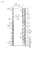
図5に示すように、第1パッド11pの幅W1pおよび第2パッド12pの幅W2pは、第1駆動線11の幅W1および第2駆動線12の幅W2よりも大きい。図6に示すように、第3パッド13pの幅W3pおよび第4パッド14pの幅W4pは、第1信号線13の幅W3および第2信号線14の幅W4よりも大きい。
Next, the
As shown in FIG. 5, the width W1p of the
第1パッド11pおよびフレキシブルプリント基板6a、第2パッド12pおよびフレキシブルプリント基板6b、第3パッド13pおよびフレキシブルプリント基板6c、並びに第4パッド14pおよびフレキシブルプリント基板6dは、それぞれフレキシブルプリント基板上のパッド部分に熱で溶融する導電性接着剤を塗布して、それぞれ両者の間隔が合うように熱圧着されている。
The
フレキシブルプリント基板6a〜6dは熱で縮む特性があり、第1ないし第4パッド11p〜14pとフレキシブルプリント基板6a〜6dのそれぞれのパッドとの間隔を合わせるため、フレキシブルプリント基板6a〜6dのそれぞれのパッドの間隔は、フレキシブルプリント基板6a〜6dの縮む量を想定して大きめに設定されている。
The flexible printed
第1パッド11pの間隔P1および第1パッド11pの幅W1の比、並びに第2パッド12pの間隔P2および第2パッド12pの幅W2の比は、それぞれ2:1が理想的であるが、上記熱圧着時の位置ずれおよび製作精度を考慮すれば、それぞれ2±0.5:1であることが望ましい。
The ratio of the spacing P1 between the
同じく、第3パッド13pの間隔P3および第3パッド13pの幅W3の比、並びに第4パッド14pの間隔P4および第4パッド14pの幅W4の比は、それぞれ2:1が理想的であるが、上記熱圧着時の位置ずれおよび製作精度を考慮すれば、それぞれ2±0.5:1であることが望ましい。
Similarly, the ratio of the distance P3 between the
以上のように構成されたX線検出器によれば、第1パッド11pの間隔P1および第2パッド12pの間隔P2は、それぞれ第1駆動線11および第2駆動線12の間隔の2倍に設定することができる。第3パッド13pの間隔P3および第4パッド14pの間隔P4は、それぞれ第1信号線13および第2信号線14の間隔の2倍に設定することができる。
According to the X-ray detector configured as described above, the interval P1 between the
このため、要求される画像分解能が高くても良好なX線検出器を提供することができる。第1駆動線11および第2駆動線12の間隔並びに第1信号線13および第2信号線14の間隔を狭くした高精細のX線検出器であっても第1ないし第4パッド11p〜14pの間隔P1〜P4を大きく設定できる利点がある。これにより、フレキシブルプリント基板6a〜6dのパッド(配線l1〜l4)の間隔は第1ないし第4パッド11p〜14pの間隔P1〜P4に合わせれば良いため、フレキシブルプリント基板6a〜6dと第1ないし第4パッド11p〜14pとを確実に接続することができ、フレキシブルプリント基板6a〜6dの光電変換基板1への固着を良好に行うことができる。
For this reason, a good X-ray detector can be provided even if the required image resolution is high. Even in a high-definition X-ray detector in which the interval between the
第1ないし第4パッド11p〜14pの間隔P1〜P4およびフレキシブルプリント基板6a〜6dのパッドの間隔を大きく設定できるため、読み取り部40aを設けた第1読み取り回路4および読み取り部40bを設けた第2読み取り回路5を光電変換基板1の周辺に容易に配置することができる。この場合でも、読み取り部40a、40bのアナログ部分の回路面積を小さくする必要は無いため、良好なノイズ特性を得ることができる。
Since the intervals P1 to P4 of the first to
第1ないし第4パッド11p〜14pの面積および間隔P1〜P4を大きく設定できるが、その面積は、第1パッド11pの幅W1pおよび第2パッド12pの幅W2pを第1駆動線11の幅W1および第2駆動線12の幅W2よりも大きくし、また、第3パッド13pの幅W3pおよび第4パッド14pの幅W4pを第1信号線13の幅W3および第2信号線14の幅W4よりも大きくすることにより実現している。このため、フレキシブルプリント基板6a〜6dと第1ないし第4パッド11p〜14pとを一層確実に接続することができる。
Although the areas of the first to
なお、この発明は、上述した実施の形態に限定されることなく、この発明の範囲内で種々変形可能である。例えば、図7に示すように、第3パッド13pと接続されるフレキシブルプリント基板6cのパッド6pの面積は大きく設定されていても良い。上記したことは、パッド6pの幅W5pを配線l3の幅W5よりも大きくすることにより実現している。上記した場合は、第3パッド13pの面積が大きく設定されていなくてもフレキシブルプリント基板6cと第3パッド13pとを一層確実に接続することができる。なお、上記したことはフレキシブルプリント基板6cに限らず、フレキシブルプリント基板6a、6b、6dのパッドの面積をフレキシブルプリント基板6cと同様大きく設定しても良い。
The present invention is not limited to the above-described embodiment, and can be variously modified within the scope of the present invention. For example, as shown in FIG. 7, the area of the
第1読み取り回路4はフレキシブルプリント基板6cを介さずに第3パッド13pと接続されても良い。上記した場合、第3パッド13pと重なった個所または第3パッド13p付近の基板10にスルーホールを形成し、スルーホールを介して第3パッド13pと基板10の裏側に設けられた第1読み取り回路4とを接続すれば良い。なお、上記したことは第1読み取り回路4に限らず、第1駆動回路2、第2駆動回路3および第2読み取り回路5もフレキシブルプリント基板を介さずにスルーホールを介して第1パッド11p、第2パッド12pおよび第4パッド14pとそれぞれ接続されても良い。
The
高精細のX線検出器を得るため、第1パッド11pと第2パッド12pとが基板10の対向する一対の辺に設けられれば良く、第3パッド13pと第4パッド14pとは基板10の対向する他の一対の辺に設けられなくても良い。
In order to obtain a high-definition X-ray detector, the
その他、高精細のX線検出器を得るため、第3パッド13pと第4パッド14pとが基板10の対向する他の一対の辺に設けられれば良く、第1パッド11pと第2パッド12pとは基板10の対向する一対の辺に設けられなくても良い。この場合、第1配線は第1信号線13、第2配線は第2信号線14、第3配線は第1駆動線11、第4配線は第2駆動線12である。
In addition, in order to obtain a high-definition X-ray detector, the
X線検出器は直接変換方式に限定されるものではなく、間接変換方式であっても上述した効果を得ることができる。この発明は、放射線検出器としてX線検出器について説明したが、これに限らずγ線等、他の放射線を検出する放射線検出器に適用することができる。 The X-ray detector is not limited to the direct conversion method, and the above-described effects can be obtained even with the indirect conversion method. Although this invention demonstrated the X-ray detector as a radiation detector, it is not restricted to this, It can apply to the radiation detector which detects other radiations, such as a gamma ray.
1…光電変換基板、2…第1駆動回路、3…第2駆動回路、4…第1読み取り回路、5…第2読み取り回路、6a,6b,6c,6d…フレキシブルプリント基板、7…操作制御部、8…制御部、10…基板、11…第1駆動線、11p…第1パッド、12…第2駆動線、12p…第2パッド、13…第1信号線、13p…第3パッド、14…第2信号線、14p…第4パッド、15…画素部、16…TFT、17…蓄積コンデンサ、19…画素電極、20…光導電層、40a,40b…読み取り部、41…電荷増幅器、50…増幅器、60…A/D変換器、70…並列/直列変換器、d1…第1方向、d2…第2方向、P1,P2,P3,P4…間隔、W1,W2,W3,W4,W1p,W2p,W3p,W4p…幅。
DESCRIPTION OF
Claims (6)
前記基板上に配設され、第1方向に互い違いに設けられ、かつ、前記第1方向に直交した第2方向にそれぞれ延出した複数の第1配線および複数の第2配線と、
前記複数の第1配線の一端に接続された複数の第1パッドと、
前記複数の第1配線に対して前記複数の第1パッドと反対側に設けられ、前記複数の第2配線の一端に接続された複数の第2パッドと、
前記第1配線および第2配線に交差して前記基板上に配設され、前記第2方向に互い違いに設けられ、かつ、前記第1方向にそれぞれ延出した複数の第3配線および複数の第4配線と、
前記第1配線、第2配線、第3配線および第4配線で囲まれたマトリクス状の複数の領域に設けられ、入射される放射線の量に対応した信号を出力する複数の画素部とを備えた放射線検出器。 A substrate,
A plurality of first wirings and a plurality of second wirings disposed on the substrate, provided alternately in a first direction, and extending in a second direction orthogonal to the first direction;
A plurality of first pads connected to one end of the plurality of first wirings;
A plurality of second pads provided on a side opposite to the plurality of first pads with respect to the plurality of first wirings and connected to one end of the plurality of second wirings;
A plurality of third wires and a plurality of third wires arranged on the substrate so as to intersect the first wires and the second wires, provided alternately in the second direction, and extending in the first direction, respectively. 4 wiring,
A plurality of pixel portions that are provided in a plurality of matrix-like regions surrounded by the first wiring, the second wiring, the third wiring, and the fourth wiring and that output signals corresponding to the amount of incident radiation; Radiation detector.
前記複数の第3配線に対して前記複数の第3パッドと反対側に設けられ、前記複数の第4配線の一端に接続された複数の第4パッドとを備えた請求項1に記載の放射線検出器。 A plurality of third pads connected to one end of the plurality of third wirings;
2. The radiation according to claim 1, further comprising: a plurality of fourth pads provided on an opposite side to the plurality of third pads with respect to the plurality of third wirings and connected to one end of the plurality of fourth wirings. Detector.
Priority Applications (1)
| Application Number | Priority Date | Filing Date | Title |
|---|---|---|---|
| JP2005284612A JP2007093449A (en) | 2005-09-29 | 2005-09-29 | Radiation detector |
Applications Claiming Priority (1)
| Application Number | Priority Date | Filing Date | Title |
|---|---|---|---|
| JP2005284612A JP2007093449A (en) | 2005-09-29 | 2005-09-29 | Radiation detector |
Publications (1)
| Publication Number | Publication Date |
|---|---|
| JP2007093449A true JP2007093449A (en) | 2007-04-12 |
Family
ID=37979343
Family Applications (1)
| Application Number | Title | Priority Date | Filing Date |
|---|---|---|---|
| JP2005284612A Withdrawn JP2007093449A (en) | 2005-09-29 | 2005-09-29 | Radiation detector |
Country Status (1)
| Country | Link |
|---|---|
| JP (1) | JP2007093449A (en) |
Cited By (3)
| Publication number | Priority date | Publication date | Assignee | Title |
|---|---|---|---|---|
| JP2012211898A (en) * | 2011-03-30 | 2012-11-01 | Ge Medical Systems Global Technology Co Llc | Flat panel imager for x-ray detector and method for disposing module |
| WO2015093134A1 (en) * | 2013-12-18 | 2015-06-25 | キヤノン株式会社 | Radiation detection device and radiation detection system |
| WO2016199820A1 (en) * | 2015-06-10 | 2016-12-15 | 東芝電子管デバイス株式会社 | Array substrate and radiation detector |
-
2005
- 2005-09-29 JP JP2005284612A patent/JP2007093449A/en not_active Withdrawn
Cited By (9)
| Publication number | Priority date | Publication date | Assignee | Title |
|---|---|---|---|---|
| JP2012211898A (en) * | 2011-03-30 | 2012-11-01 | Ge Medical Systems Global Technology Co Llc | Flat panel imager for x-ray detector and method for disposing module |
| WO2015093134A1 (en) * | 2013-12-18 | 2015-06-25 | キヤノン株式会社 | Radiation detection device and radiation detection system |
| WO2016199820A1 (en) * | 2015-06-10 | 2016-12-15 | 東芝電子管デバイス株式会社 | Array substrate and radiation detector |
| JP2017003426A (en) * | 2015-06-10 | 2017-01-05 | 東芝電子管デバイス株式会社 | Array substrate and radiation detector |
| KR20170134672A (en) * | 2015-06-10 | 2017-12-06 | 도시바 덴시칸 디바이스 가부시키가이샤 | Array substrate and radiation detector |
| CN107533148A (en) * | 2015-06-10 | 2018-01-02 | 东芝电子管器件株式会社 | Array base palte and ray detector |
| US20180040636A1 (en) * | 2015-06-10 | 2018-02-08 | Toshiba Electron Tubes & Devices Co., Ltd. | Array substrate and radiation detector |
| US10276602B2 (en) | 2015-06-10 | 2019-04-30 | Canon Electron Tubes & Devices Co., Ltd. | Array substrate and radiation detector |
| KR102001168B1 (en) * | 2015-06-10 | 2019-07-17 | 캐논 덴시칸 디바이스 가부시키가이샤 | Array substrate and radiation detector |
Similar Documents
| Publication | Publication Date | Title |
|---|---|---|
| JP5235350B2 (en) | Imaging apparatus and radiation imaging system | |
| JP4307322B2 (en) | Radiation imaging apparatus and radiation imaging system | |
| JP4750512B2 (en) | Radiation imaging apparatus, control method therefor, and radiation imaging system | |
| EP1687971B1 (en) | Radiation image pick-up device and method therefor, and radiation image pick-up system | |
| JP4845352B2 (en) | Radiation imaging apparatus, manufacturing method thereof, and radiation imaging system | |
| JP5159065B2 (en) | Radiation detection apparatus, radiation imaging apparatus, and radiation imaging system | |
| JP5376897B2 (en) | Radiation imaging equipment | |
| US6956216B2 (en) | Semiconductor device, radiation detection device, and radiation detection system | |
| WO2010070735A1 (en) | Optical matrix device | |
| JP5886793B2 (en) | Solid-state imaging device | |
| JP2012038857A (en) | Detector and radiation detection system | |
| JP2011023426A (en) | Image capturing apparatus and radiation imaging system | |
| JP5508831B2 (en) | X-ray image detector | |
| CN104584535B (en) | Current/voltage converter circuit and imaging device | |
| JPH1093061A (en) | Image-detecting apparatus, array substrate and manufacturing the image-detecting apparatus | |
| JP2007184407A (en) | Electromagnetic wave detection device and radiation imaging system | |
| JP2007093449A (en) | Radiation detector | |
| US7557354B2 (en) | Radiation image detector | |
| JP4408593B2 (en) | Radiation detection apparatus and system | |
| JP5677353B2 (en) | Radiation detection apparatus and radiation imaging system | |
| JP6719324B2 (en) | Radiation imaging apparatus and radiation imaging system | |
| JP2002124676A (en) | Semiconductor device | |
| JP3467027B2 (en) | Semiconductor device, radiation detection device, and radiation imaging system | |
| JP3545130B2 (en) | Solid-state imaging device | |
| KR102392314B1 (en) | Solid-state imaging device, radiation imaging system, and control method of solid-state imaging device |
Legal Events
| Date | Code | Title | Description |
|---|---|---|---|
| A300 | Application deemed to be withdrawn because no request for examination was validly filed |
Free format text: JAPANESE INTERMEDIATE CODE: A300 Effective date: 20081202 |