JP2007073790A - Wiring member locking device and electronic device casing - Google Patents
Wiring member locking device and electronic device casing Download PDFInfo
- Publication number
- JP2007073790A JP2007073790A JP2005260186A JP2005260186A JP2007073790A JP 2007073790 A JP2007073790 A JP 2007073790A JP 2005260186 A JP2005260186 A JP 2005260186A JP 2005260186 A JP2005260186 A JP 2005260186A JP 2007073790 A JP2007073790 A JP 2007073790A
- Authority
- JP
- Japan
- Prior art keywords
- wiring member
- electronic device
- cabinet
- liquid crystal
- wiring
- Prior art date
- Legal status (The legal status is an assumption and is not a legal conclusion. Google has not performed a legal analysis and makes no representation as to the accuracy of the status listed.)
- Pending
Links
Images


Landscapes
- Mounting Of Printed Circuit Boards And The Like (AREA)
- Devices For Indicating Variable Information By Combining Individual Elements (AREA)
Abstract
【課題】 薄型表示装置など電子機器の筐体に配設された放熱孔を経由し静電気帯電した人体やその他の物品から該電子機器内部の配線部材に放電し、該配線部材に接続された半導体部品の絶縁破壊不良が発生することを防止するための該配線部材の通過位置規制手段を提供する。
【解決手段】 FPCやFFCなどの配線部材24の側縁部を該印刷配線基板取り付け用の樹脂成型シャーシ6と一体に形成したクランパ6aaまたはおよび6abにより係止し、または該配線部材24が近接するキャビネット内面の排気孔の近傍に該キャビネットの内面の法線方向に薄板状の隔壁を形成し、該排気孔および該配線部材24の空間距離を維持する。
【選択図】 図4PROBLEM TO BE SOLVED To provide a semiconductor connected to a wiring member discharged from a statically charged human body or other article to a wiring member inside the electronic device through a heat radiating hole disposed in a casing of the electronic device such as a thin display device. Provided is a means for restricting the passage position of the wiring member for preventing occurrence of defective dielectric breakdown of components.
A side edge of a wiring member 24 such as FPC or FFC is locked by a clamper 6aa or 6ab integrally formed with a resin molding chassis 6 for mounting the printed wiring board, or the wiring member 24 is in proximity. In the vicinity of the exhaust hole on the inner surface of the cabinet, a thin plate-like partition is formed in the normal direction of the inner surface of the cabinet, and the space distance between the exhaust hole and the wiring member 24 is maintained.
[Selection] Figure 4
Description
本発明は液晶表示パネルやPDPを表示素子とする薄型表示装置その他の電子機器内部のFPCやFFCなどの配線部材の係止装置、および放熱孔を具備する電子機器筐体に関するもので、詳しくは該配線部材および該電子機器筐体面に穿設された放熱孔との空間距離を維持する手段を提供するものである。
BACKGROUND OF THE
液晶表示パネルやPDPを表示素子とするテレビやデータディスプレイなどの薄型表示装置は、従来のブラウン管を表示素子とした表示装置と比較しフラットな大画面、薄型、軽量、省電力などの多くの特長を有することから急速に需要が拡大している。特に充分な設置場所の確保が困難な設置環境条件下においても大型表示画面を享受できる薄型表示装置の特長を確固たるものとすべく更なる薄型化実現の努力が払われている。 Thin display devices such as TVs and data displays using liquid crystal display panels and PDP as display elements have many features such as a large flat screen, thin shape, light weight, and power saving compared to conventional display devices using cathode ray tubes. Demand is expanding rapidly. In particular, efforts are being made to realize further thinning in order to secure the features of a thin display device that can enjoy a large display screen even under installation environment conditions in which it is difficult to secure a sufficient installation location.
薄型表示装置の更なる薄型化実現の一手段として、該薄型表示装置内に配設される多数の印刷配線基板相互間や該印刷配線基板と表示パネル間の多数の回路を一挙に接続することが可能な配線部材としてフィルム状のFPC(Flexible Printed Circuit)やFFC(Flexible Flat Cable)などの配線部材を適用すると共に、該薄型表示装置のキャビネット内に配設された該配線部材や印刷配線基板を含む電子回路部品および該キャビネット内面の空間を可及的に小さくしている。 As a means of realizing further thinning of the thin display device, a large number of circuits between the printed wiring boards disposed in the thin display device and between the printed wiring board and the display panel are connected at a time. film-like FPC (F lexible P rinted C ircuit ) or FFC (F lexible F lat C able ) while applying a wiring member such as the disposed in the cabinet of the thin-type display device as a wiring member capable Electronic circuit components including wiring members and printed wiring boards and the space inside the cabinet are made as small as possible.
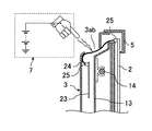
図1(b)は薄型表示装置としての液晶テレビの背面図を示している。図1(b)中の切断線C−Cで切断した縦断面図である図6に示すごとく該薄型表示装置内で発生する熱を大気中に放散し効率よくキャビネット内部を冷却するために多数の排気孔3abが後キャビネット3の上部に穿設されている。該後キャビネット3に穿設された排気孔3abの外面の至近位置に人体やその他の静電気帯電物7が接近または接触した場合に、該薄型表示装置の該後キャビネット3上部の該排気孔3abを経由し至近距離に位置する該薄型表示装置内のFPCやFFCなどの配線部材24(以下、単に配線部材と言う)を含む電子回路部品の導電体に放電し、該導電体に接続された半導体部品の絶縁破壊不良を惹起させることがある。
FIG. 1B shows a rear view of a liquid crystal television as a thin display device. As shown in FIG. 6 which is a longitudinal sectional view cut along a cutting line CC in FIG. 1B, a large number of heats are generated to dissipate heat generated in the thin display device into the atmosphere and efficiently cool the inside of the cabinet. The exhaust hole 3ab is formed in the upper part of the
電子回路中のMOS型半導体は100ボルト前後の過電圧で絶縁破壊され不良を発生するのに対し、冬季の乾燥期に人体に帯電する静電気電圧は10キロボルト以上に達することがあり、前記後キャビネットに穿設された排気孔を経由し、人体やその他の静電気帯電物が筐体内部の配線部材を含む電子回路部品に放電し該電子回路中の半導体部品の絶縁不良が発生することを防止するため、通過位置が不安定な該キャビネット内部の配線部材および該後キャビネットに穿設された排気孔間に充分な空間距離を維持する必要がある。 While MOS type semiconductors in electronic circuits break down due to overvoltage of around 100 volts and cause defects, the electrostatic voltage charged on the human body during the dry season in winter may reach 10 kilovolts or more, In order to prevent a human body or other electrostatically charged material from being discharged to an electronic circuit component including a wiring member inside the housing through a drilled exhaust hole and causing an insulation failure of a semiconductor component in the electronic circuit. It is necessary to maintain a sufficient space distance between the wiring member in the cabinet where the passage position is unstable and the exhaust hole formed in the rear cabinet.
配線部材の通過位置を規制するための従来例としては、特許文献1に見られるごとく印刷配線基板端面に配線挿入口および配線係止孔を設け配線部材を係止する。または特許文献2に見られるごとく印刷配線基板支持体の一部に配線係止部を設け係止しているが、いずれも絶縁被覆電線を係止することを意図したものであり、FPCやFFCなどの配線部材の通過位置を合理的に規制する手段ではなかった。
薄型表示装置の後キャビネットに配設された放熱孔の外面の至近位置に人体やその他の静電気帯電物が接近または接触した場合に、該薄型表示装置の該後キャビネットの放熱孔を経由し至近距離に位置する該薄型表示装置内の配線部材を含む電子回路部品の導電体に放電し、該導電体に接続された半導体部品の絶縁破壊不良を発生させる不都合を惹起することがある。 When a human body or other electrostatically charged material approaches or comes into contact with the outer surface of the heat dissipation hole disposed in the rear cabinet of the thin display device, the closest distance via the heat dissipation hole of the rear cabinet of the thin display device In some cases, the electric conductor of the electronic circuit component including the wiring member in the thin display device is discharged to the electric conductor, causing a problem of causing a breakdown failure of the semiconductor component connected to the electric conductor.
特にFPCやFFCなどのプラスチックフィルム面に導体を形成した配線部材では該導電体への過剰な機械的ストレスによる該導電体の断線事故防止のため折り曲げ部に一定以上の屈曲半径を維持する必要があり、また該配線部材を構成するプラスチックフィルム部材が有するスプリングアクションにより通過経路が大きな円弧を描くため、後キャビネット内面に接触しやすくなるため確実な配線部材の通過位置規制手段を必要とする。また、設計上又は生産上の都合、例えば、異機種間での部品の共通化や、生産現場での管理を容易にするため、過去のモデルで使用した既存の部品を流用することも多い。この場合、前記配線部材の通過位置規制手段として短いものは使えず、長目のものを使用せざるを得ないため、さらに後キャビネット内面に接触しやすくなるため確実な配線部材の通過位置規制手段を必要とする。 In particular, in a wiring member in which a conductor is formed on the surface of a plastic film such as FPC or FFC, it is necessary to maintain a bending radius of a certain level or more in the bent portion in order to prevent disconnection accident of the conductor due to excessive mechanical stress on the conductor. In addition, since the passage route draws a large arc by the spring action of the plastic film member constituting the wiring member, it is easy to come into contact with the inner surface of the rear cabinet, so that a reliable passage position regulating means for the wiring member is required. Also, in order to facilitate design or production convenience, for example, sharing of parts between different models and management at the production site, existing parts used in past models are often diverted. In this case, the short passage position restricting means for the wiring member cannot be used, and the longer one must be used, so that it is easy to contact the inner surface of the rear cabinet. Need.
電子機器内部の印刷配線基板相互の接続、または印刷配線基板および他の電子回路部品間を接続するFPCやFFCなどの配線部材の側縁部を係止するため爪状に形成された少なくともひとつの配線部材係止用クランパを印刷配線基板取り付け用樹脂成型シャーシと一体に形成する。 At least one claw-like shape that is used to lock the side edges of wiring members such as FPC and FFC that connect printed wiring boards inside an electronic device or between printed wiring boards and other electronic circuit components. A wiring member locking clamper is formed integrally with a resin molded chassis for mounting a printed wiring board.
電子機器内部の印刷配線基板相互の接続、または印刷配線基板および他の電子回路部品間を接続するFPCやFFCなどの配線部材の通過位置を規制し、該電子機器のキャビネット面に穿設された放熱孔との空間距離を維持するため、該配線部材が近接する該キャビネット内面の該放熱孔近傍に、該キャビネット内面の法線方向に突起する隔壁を形成する。 The position of passage of wiring members such as FPC and FFC that connect printed wiring boards inside the electronic device or between the printed wiring board and other electronic circuit components is regulated, and is drilled on the cabinet surface of the electronic device. In order to maintain a spatial distance from the heat radiating hole, a partition wall protruding in the normal direction of the cabinet inner surface is formed in the vicinity of the heat radiating hole of the cabinet inner surface close to the wiring member.
FPCやFFCなどの配線部材を構成する導電体への過剰な機械的ストレスによる該導電体の断線事故防止のため該配線部材の折り曲げ部には一定以上の屈曲半径を維持する必要がある該FPCやFFCなどの配線部材において確実に通過位置を規制し、該配線部材および電子機器の筐体面に穿設された放熱孔との空間距離を維持することが可能となり、後キャビネットに穿設された放熱孔外面の至近位置に人体やその他の静電気帯電物が接近または接触した場合においても、該人体やその他の静電気帯電物から該配線部材を含む電子回路部品への静電気放電による該電子回路中の半導体部品の絶縁破壊不良の発生を防止することが可能となる。 It is necessary to maintain a bending radius of a certain level or more at the bent portion of the wiring member in order to prevent disconnection accident of the conductive member due to excessive mechanical stress on the conductive member constituting the wiring member such as FPC or FFC In the wiring member such as FFC, it is possible to reliably regulate the passing position and maintain the space distance between the wiring member and the heat radiation hole formed in the housing surface of the electronic device. Even when a human body or other electrostatically charged material approaches or comes into contact with a position close to the outer surface of the heat dissipation hole, the electronic circuit in the electronic circuit is caused by electrostatic discharge from the human body or other electrostatically charged material to the electronic circuit component including the wiring member. It becomes possible to prevent the occurrence of defective breakdown of semiconductor components.
以下、図に基づき本発明の実施形態を適用した薄型表示装置としての液晶テレビについて説明する。図1(a)は液晶テレビ1の外観正面図、図1(b)は該液晶テレビ1の背面図である。図1において、2は画像表示を行う液晶表示パネル3は後キャビネット、3aaは該液晶テレビ内部における発生熱を筐体外に放散し冷却するための外気の吸気孔、3abは排気孔、4は液晶テレビ1を卓上型として使用する場合に適用されるスタンド、5は前キャビネットである。
Hereinafter, a liquid crystal television as a thin display device to which an embodiment of the present invention is applied will be described with reference to the drawings. FIG. 1A is an external front view of the
次に、図2に基づき液晶テレビ内部の光学システムの概要構成を説明する。液晶表示パネル2の背面側には、液晶表示画面の高輝度化や面輝度均一化などの画像品位改善のため光反射、偏光、屈折、光拡散などの高度の光制御技術を利用し表面に多数のマイクロレンズアレイを形成するなどの手段を適用した複数のフィルムにより構成される光学シートセット11が配設されている。さらに該光学シートセット11の後方には該光学シートセット11および該液晶表示パネル2の背面から光照射するためのバックライトユニット19が配設されている。該バックライトユニット19はバックライトシャーシ13内部に多数の発光管14および光拡散板12が配設されている。
Next, a schematic configuration of the optical system inside the liquid crystal television will be described with reference to FIG. On the back side of the liquid
図3は本発明の実施形態を示す液晶テレビの後キャビネットを取り除き、内部の主要構成部品の配置関係を示す斜視図である。液晶表示パネル2の背面には該液晶表示パネル2の背面から光照射するためのバックライトユニットを構成するバックライトシャーシ13が配設されている。さらに該バックライトシャーシ13の背面には液晶テレビの電気回路を構成する信号処理基板22や液晶表示パネルコントローラ基板23などの複数の印刷配線基板が取り付けられている。該液晶表示パネルコントローラ基板23および該液晶表示パネル2はコネクタ25を介し、FPCやFFCなどの配線部材24により接続されている。
FIG. 3 is a perspective view showing the arrangement relationship of the main components inside the LCD TV according to the embodiment of the present invention with the rear cabinet removed. A
図4は本発明の第1の実施例を説明するための液晶表示パネル2および液晶表示パネルコントローラ基板23を接続するFPCやFFCなどの配線部材24部分を詳細に示す拡大斜視図である。FPCやFFCなどの配線部材24は液晶表示パネルコントローラ基板23側に装着されたコネクタ25および液晶表示パネル2側に装着されたコネクタ25間を接続している。配線部材24はプラスチックフィルム面に多数の導電体を印刷技術により形成し、該導電体表面がさらにプラスチック薄膜絶縁体で覆われている。該配線部材の薄型化と柔軟性を維持する必要から該プラスチック絶縁体の膜厚は薄く耐電圧は500ボルト程度に設定されているが、本発明による液晶テレビでは通常の使用条件において問題なく使用することが可能である。
FIG. 4 is an enlarged perspective view showing in detail a portion of a
図5は、本発明の第1の実施例の変形例を示し、樹脂成型シャーシ6の第1及び第2のクランパを傾斜して形成したものであり、図示するごとく第1のクランパ6aa’及び第2のクランパ6ab’を傾斜して形成してある。それ以外の構成は図4の構成と同一である。このように傾斜して形成することにより、FPCやFFCなどの配線部材24部分を更に適切に位置決めし保持することが可能となる。すなわち、傾斜して形成された第1のクランパ6aa’及び第2のクランパ6ab’によりFPCやFFCなどの配線部材24部分が後キャビネット3側に変位するのを規制することが可能となる。
FIG. 5 shows a modification of the first embodiment of the present invention, in which the first and second clampers of the resin-molded
しかしながら該配線部材24が液晶テレビキャビネットの放熱孔などの開口部を通じキャビネットの外部から冬季の乾燥期には10キロボルト以上にも達する人体などの静電気帯電物が接触または近接した場合には、該配線部材24の該プラスチック薄膜絶縁体の絶縁を破壊し該配線部材を構成する導電体に放電する。放電電圧は該配線部材24の導電体を通じ該導電体に接続されたMOS型半導体などの集積回路部品やトランジスタにも印加され、これらの半導体の絶縁破壊不良を発生させる原因となる。
However, if an electrostatically charged object such as a human body that reaches 10 kilovolts or more from the outside of the cabinet through the opening such as a heat radiating hole of the liquid crystal television cabinet from the outside of the cabinet comes into contact or close to the
図7の従来例に示すごとく配線部材24を構成するプラスチック構成部材が有するスプリングアクションにより該配線部材24の通過経路は、該配線部材24が接続される複数のコネクタ25の2点間に大きな円弧を描き、後キャビネット3の上部に穿設された排気孔3abに接近または接触する。このような状態を回避するため図4に示すごとく第1のクランパ6aaおよびまたは第2のクランパ6abを印刷配線基板支持用の樹脂成型シャーシ6と共に一体に成型し、該配線部材24の少なくとも側縁部のひとつを挟持し、配線部材24の通過経路を規制することにより該配線部材24およびキャビネットに穿設された排気孔との空間距離を確保し、該キャビネットに穿設された放熱孔を通じ該キャビネット外表面に近接または接触した静電気帯電物が該配線部材24に放電することを防止することが可能となる。
As shown in the conventional example of FIG. 7, the passage path of the
図6は本発明の第2の実施形態を説明するため図1中に示す切断線C−Cに沿って切断した縦断面を示す斜視図である。後キャビネット3の上部に穿設された複数の排気孔3abの仕切り部分3dの内面の法線方向に薄板状の複数の隔壁3cが後キャビネット3と共に一体に成型されている。
FIG. 6 is a perspective view showing a longitudinal section taken along a cutting line CC shown in FIG. 1 for explaining a second embodiment of the present invention. A plurality of
FPCやFFCなどの配線部材24および該後キャビネット3の上部に穿設された排気孔3abは該隔壁3cにより相互に隔てられ、該排気孔3abの外面に接近又は接触する静電気帯電物および後キャビネット3内部の配線部材24との空間距離を維持することが可能となり10キロボルト以上にも及ぶ静電気該帯電物の静電気が該配線部材24に放電することを防止し、該配線部材24に接続される半導体部品の絶縁破壊不良の発生を防止することが可能となる。また該配線部材24が排気孔3abを閉塞しキャビネット内部での発生熱の放熱効果を低下させることをも防止することが出来る。
The
1: 液晶テレビ
2: 液晶表示パネル
3: 後キャビネット
3a: 放熱孔
3aa: 吸気孔
3ab: 排気孔
3b: 突起
3c: 隔壁
3d: 仕切り部分
4: スタンド
5: 前キャビネット
6: 樹脂成型シャーシ
6a: クランパ
6aa、 6aa’: 第1のクランパ
6ab、 6ab’: 第2のクランパ
7: 静電気帯電物
11: 光学シートセット
12: 光拡散板
13: バックライトシャーシ
14: 発光管
19: バックライトユニット
22: 信号処理基板
23: 液晶表示パネルコントローラ基板
24: 配線部材
25: コネクタ
1: LCD TV 2: Liquid Crystal Display Panel 3: Rear Cabinet 3a: Heat Dissipation Hole 3aa: Intake Hole 3ab: Exhaust Hole 3b:
Claims (2)
Priority Applications (1)
| Application Number | Priority Date | Filing Date | Title |
|---|---|---|---|
| JP2005260186A JP2007073790A (en) | 2005-09-08 | 2005-09-08 | Wiring member locking device and electronic device casing |
Applications Claiming Priority (1)
| Application Number | Priority Date | Filing Date | Title |
|---|---|---|---|
| JP2005260186A JP2007073790A (en) | 2005-09-08 | 2005-09-08 | Wiring member locking device and electronic device casing |
Publications (1)
| Publication Number | Publication Date |
|---|---|
| JP2007073790A true JP2007073790A (en) | 2007-03-22 |
Family
ID=37934971
Family Applications (1)
| Application Number | Title | Priority Date | Filing Date |
|---|---|---|---|
| JP2005260186A Pending JP2007073790A (en) | 2005-09-08 | 2005-09-08 | Wiring member locking device and electronic device casing |
Country Status (1)
| Country | Link |
|---|---|
| JP (1) | JP2007073790A (en) |
Cited By (1)
| Publication number | Priority date | Publication date | Assignee | Title |
|---|---|---|---|---|
| CN101750777B (en) * | 2008-12-15 | 2012-09-05 | 乐金显示有限公司 | liquid crystal display device |
Citations (10)
| Publication number | Priority date | Publication date | Assignee | Title |
|---|---|---|---|---|
| JPS6352268U (en) * | 1986-09-24 | 1988-04-08 | ||
| JPH0338679U (en) * | 1989-08-26 | 1991-04-15 | ||
| JPH0590989U (en) * | 1992-05-01 | 1993-12-10 | 山武ハネウエル株式会社 | Air conditioning controller |
| JPH05347488A (en) * | 1991-03-06 | 1993-12-27 | Fujitsu Ltd | Mounting structure for desk-top electronic apparatus on cabinet shelf |
| JPH06112668A (en) * | 1992-09-28 | 1994-04-22 | Sony Corp | Belt type cord mounting structure |
| JPH06120677A (en) * | 1992-10-05 | 1994-04-28 | Meisei Electric Co Ltd | Ventilation structure for housing |
| JPH09162571A (en) * | 1995-12-12 | 1997-06-20 | Sumitomo Wiring Syst Ltd | Attaching structure of flexible printed circuit to fixing member |
| JPH1013060A (en) * | 1996-06-26 | 1998-01-16 | Alps Electric Co Ltd | Mounting structure of flexible circuit board and recording/reproducing device using it |
| JP2000323878A (en) * | 1999-05-12 | 2000-11-24 | Matsushita Electric Ind Co Ltd | Electronic equipment cooling structure |
| JP2002091335A (en) * | 2000-09-13 | 2002-03-27 | Seiko Epson Corp | Flexible PCB case and LCD module |
-
2005
- 2005-09-08 JP JP2005260186A patent/JP2007073790A/en active Pending
Patent Citations (10)
| Publication number | Priority date | Publication date | Assignee | Title |
|---|---|---|---|---|
| JPS6352268U (en) * | 1986-09-24 | 1988-04-08 | ||
| JPH0338679U (en) * | 1989-08-26 | 1991-04-15 | ||
| JPH05347488A (en) * | 1991-03-06 | 1993-12-27 | Fujitsu Ltd | Mounting structure for desk-top electronic apparatus on cabinet shelf |
| JPH0590989U (en) * | 1992-05-01 | 1993-12-10 | 山武ハネウエル株式会社 | Air conditioning controller |
| JPH06112668A (en) * | 1992-09-28 | 1994-04-22 | Sony Corp | Belt type cord mounting structure |
| JPH06120677A (en) * | 1992-10-05 | 1994-04-28 | Meisei Electric Co Ltd | Ventilation structure for housing |
| JPH09162571A (en) * | 1995-12-12 | 1997-06-20 | Sumitomo Wiring Syst Ltd | Attaching structure of flexible printed circuit to fixing member |
| JPH1013060A (en) * | 1996-06-26 | 1998-01-16 | Alps Electric Co Ltd | Mounting structure of flexible circuit board and recording/reproducing device using it |
| JP2000323878A (en) * | 1999-05-12 | 2000-11-24 | Matsushita Electric Ind Co Ltd | Electronic equipment cooling structure |
| JP2002091335A (en) * | 2000-09-13 | 2002-03-27 | Seiko Epson Corp | Flexible PCB case and LCD module |
Cited By (1)
| Publication number | Priority date | Publication date | Assignee | Title |
|---|---|---|---|---|
| CN101750777B (en) * | 2008-12-15 | 2012-09-05 | 乐金显示有限公司 | liquid crystal display device |
Similar Documents
| Publication | Publication Date | Title |
|---|---|---|
| EP3787383B1 (en) | Image displaying apparatus | |
| US7364442B2 (en) | Fixing structure of circuit board and display module comprising the same | |
| KR102260801B1 (en) | Display Device | |
| US8013529B2 (en) | Plasma display device | |
| US7894035B2 (en) | Driving device and a liquid crystal display including the same | |
| US9618688B2 (en) | Display device | |
| US20100177479A1 (en) | Flat-panel display apparatus | |
| KR20060042756A (en) | Heat dissipation structure of display panel and display module having same | |
| WO2017049882A1 (en) | Backlight module and display device | |
| KR20080077827A (en) | Light emitting diode block, backlight unit and liquid crystal display using the same | |
| KR100670364B1 (en) | Plasma display device | |
| US20060291153A1 (en) | Plasma display module | |
| JP2007073790A (en) | Wiring member locking device and electronic device casing | |
| US20070159777A1 (en) | Chassis assembly and display apparatus having the same | |
| KR100420036B1 (en) | Plasma Display Device | |
| US8471978B2 (en) | Driving device and a liquid crystal display including the same | |
| US20070001565A1 (en) | Flat Display Device | |
| JP2006330354A (en) | Display device | |
| CN216563134U (en) | Display module and display panel | |
| KR100813848B1 (en) | Plasma display device | |
| KR100659102B1 (en) | Plasma display device | |
| KR100751367B1 (en) | Plasma display device | |
| KR20080037964A (en) | Plasma display device | |
| KR20070058182A (en) | Backlight unit and liquid crystal display including the same |
Legal Events
| Date | Code | Title | Description |
|---|---|---|---|
| A621 | Written request for application examination |
Free format text: JAPANESE INTERMEDIATE CODE: A621 Effective date: 20070822 |
|
| A977 | Report on retrieval |
Free format text: JAPANESE INTERMEDIATE CODE: A971007 Effective date: 20090916 |
|
| A131 | Notification of reasons for refusal |
Free format text: JAPANESE INTERMEDIATE CODE: A131 Effective date: 20090929 |
|
| A521 | Written amendment |
Free format text: JAPANESE INTERMEDIATE CODE: A523 Effective date: 20091120 |
|
| A131 | Notification of reasons for refusal |
Free format text: JAPANESE INTERMEDIATE CODE: A131 Effective date: 20100119 |
|
| A02 | Decision of refusal |
Free format text: JAPANESE INTERMEDIATE CODE: A02 Effective date: 20100706 |