JP2006507411A - Method for forming oxide thin film using negative sputter ion beam source - Google Patents
Method for forming oxide thin film using negative sputter ion beam source Download PDFInfo
- Publication number
- JP2006507411A JP2006507411A JP2004555480A JP2004555480A JP2006507411A JP 2006507411 A JP2006507411 A JP 2006507411A JP 2004555480 A JP2004555480 A JP 2004555480A JP 2004555480 A JP2004555480 A JP 2004555480A JP 2006507411 A JP2006507411 A JP 2006507411A
- Authority
- JP
- Japan
- Prior art keywords
- thin film
- oxide
- substrate
- oxide thin
- sputter target
- Prior art date
- Legal status (The legal status is an assumption and is not a legal conclusion. Google has not performed a legal analysis and makes no representation as to the accuracy of the status listed.)
- Withdrawn
Links
- 239000010409 thin film Substances 0.000 title claims abstract description 110
- 238000000034 method Methods 0.000 title claims abstract description 43
- 238000010884 ion-beam technique Methods 0.000 title description 37
- 239000000758 substrate Substances 0.000 claims abstract description 44
- 238000012545 processing Methods 0.000 claims abstract description 26
- MYMOFIZGZYHOMD-UHFFFAOYSA-N Dioxygen Chemical compound O=O MYMOFIZGZYHOMD-UHFFFAOYSA-N 0.000 claims abstract description 18
- 229910001882 dioxygen Inorganic materials 0.000 claims abstract description 18
- 150000002500 ions Chemical class 0.000 claims abstract description 16
- 239000011261 inert gas Substances 0.000 claims abstract description 11
- 239000003638 chemical reducing agent Substances 0.000 claims abstract description 9
- 238000005477 sputtering target Methods 0.000 claims abstract description 4
- 229910004298 SiO 2 Inorganic materials 0.000 claims description 51
- VYPSYNLAJGMNEJ-UHFFFAOYSA-N Silicium dioxide Chemical compound O=[Si]=O VYPSYNLAJGMNEJ-UHFFFAOYSA-N 0.000 claims description 18
- 229910052792 caesium Inorganic materials 0.000 claims description 17
- TVFDJXOCXUVLDH-UHFFFAOYSA-N caesium atom Chemical compound [Cs] TVFDJXOCXUVLDH-UHFFFAOYSA-N 0.000 claims description 17
- GWEVSGVZZGPLCZ-UHFFFAOYSA-N Titan oxide Chemical compound O=[Ti]=O GWEVSGVZZGPLCZ-UHFFFAOYSA-N 0.000 claims description 14
- 235000012239 silicon dioxide Nutrition 0.000 claims description 9
- 239000000377 silicon dioxide Substances 0.000 claims description 9
- 238000004544 sputter deposition Methods 0.000 claims description 6
- OGIDPMRJRNCKJF-UHFFFAOYSA-N titanium oxide Inorganic materials [Ti]=O OGIDPMRJRNCKJF-UHFFFAOYSA-N 0.000 claims description 6
- 238000001755 magnetron sputter deposition Methods 0.000 claims description 5
- BPUBBGLMJRNUCC-UHFFFAOYSA-N oxygen(2-);tantalum(5+) Chemical compound [O-2].[O-2].[O-2].[O-2].[O-2].[Ta+5].[Ta+5] BPUBBGLMJRNUCC-UHFFFAOYSA-N 0.000 claims description 5
- 229910018072 Al 2 O 3 Inorganic materials 0.000 claims description 4
- CJNBYAVZURUTKZ-UHFFFAOYSA-N hafnium(iv) oxide Chemical compound O=[Hf]=O CJNBYAVZURUTKZ-UHFFFAOYSA-N 0.000 claims description 4
- URLJKFSTXLNXLG-UHFFFAOYSA-N niobium(5+);oxygen(2-) Chemical compound [O-2].[O-2].[O-2].[O-2].[O-2].[Nb+5].[Nb+5] URLJKFSTXLNXLG-UHFFFAOYSA-N 0.000 claims description 4
- TWNQGVIAIRXVLR-UHFFFAOYSA-N oxo(oxoalumanyloxy)alumane Chemical compound O=[Al]O[Al]=O TWNQGVIAIRXVLR-UHFFFAOYSA-N 0.000 claims description 4
- 230000008569 process Effects 0.000 claims description 4
- 239000011734 sodium Substances 0.000 claims description 4
- DGAQECJNVWCQMB-PUAWFVPOSA-M Ilexoside XXIX Chemical compound C[C@@H]1CC[C@@]2(CC[C@@]3(C(=CC[C@H]4[C@]3(CC[C@@H]5[C@@]4(CC[C@@H](C5(C)C)OS(=O)(=O)[O-])C)C)[C@@H]2[C@]1(C)O)C)C(=O)O[C@H]6[C@@H]([C@H]([C@@H]([C@H](O6)CO)O)O)O.[Na+] DGAQECJNVWCQMB-PUAWFVPOSA-M 0.000 claims description 3
- WHXSMMKQMYFTQS-UHFFFAOYSA-N Lithium Chemical compound [Li] WHXSMMKQMYFTQS-UHFFFAOYSA-N 0.000 claims description 3
- ZLMJMSJWJFRBEC-UHFFFAOYSA-N Potassium Chemical compound [K] ZLMJMSJWJFRBEC-UHFFFAOYSA-N 0.000 claims description 3
- 238000010521 absorption reaction Methods 0.000 claims description 3
- 229910052744 lithium Inorganic materials 0.000 claims description 3
- 229910052700 potassium Inorganic materials 0.000 claims description 3
- 239000011591 potassium Substances 0.000 claims description 3
- 229910052701 rubidium Inorganic materials 0.000 claims description 3
- IGLNJRXAVVLDKE-UHFFFAOYSA-N rubidium atom Chemical compound [Rb] IGLNJRXAVVLDKE-UHFFFAOYSA-N 0.000 claims description 3
- 229910052708 sodium Inorganic materials 0.000 claims description 3
- 229910001936 tantalum oxide Inorganic materials 0.000 claims description 3
- 238000010494 dissociation reaction Methods 0.000 claims 1
- 230000005593 dissociations Effects 0.000 claims 1
- 238000012856 packing Methods 0.000 abstract description 7
- 230000003746 surface roughness Effects 0.000 abstract description 5
- 239000007789 gas Substances 0.000 abstract description 3
- 238000005452 bending Methods 0.000 description 22
- 238000000151 deposition Methods 0.000 description 21
- 230000008859 change Effects 0.000 description 20
- 230000008021 deposition Effects 0.000 description 18
- 238000002834 transmittance Methods 0.000 description 14
- 230000003679 aging effect Effects 0.000 description 12
- 238000000089 atomic force micrograph Methods 0.000 description 10
- QVGXLLKOCUKJST-UHFFFAOYSA-N atomic oxygen Chemical compound [O] QVGXLLKOCUKJST-UHFFFAOYSA-N 0.000 description 10
- 239000010408 film Substances 0.000 description 10
- 239000011521 glass Substances 0.000 description 10
- 239000001301 oxygen Substances 0.000 description 10
- 229910052760 oxygen Inorganic materials 0.000 description 10
- XKRFYHLGVUSROY-UHFFFAOYSA-N Argon Chemical compound [Ar] XKRFYHLGVUSROY-UHFFFAOYSA-N 0.000 description 9
- 150000001450 anions Chemical class 0.000 description 9
- 230000033001 locomotion Effects 0.000 description 7
- XUIMIQQOPSSXEZ-UHFFFAOYSA-N Silicon Chemical compound [Si] XUIMIQQOPSSXEZ-UHFFFAOYSA-N 0.000 description 6
- 238000005259 measurement Methods 0.000 description 6
- 229910052710 silicon Inorganic materials 0.000 description 6
- 239000010703 silicon Substances 0.000 description 6
- 229910052786 argon Inorganic materials 0.000 description 5
- 230000008901 benefit Effects 0.000 description 5
- 230000008033 biological extinction Effects 0.000 description 5
- 239000002245 particle Substances 0.000 description 5
- 230000007423 decrease Effects 0.000 description 4
- 239000011248 coating agent Substances 0.000 description 2
- 238000000576 coating method Methods 0.000 description 2
- 238000005137 deposition process Methods 0.000 description 2
- 238000010586 diagram Methods 0.000 description 2
- 238000005530 etching Methods 0.000 description 2
- -1 for example Substances 0.000 description 2
- 238000007735 ion beam assisted deposition Methods 0.000 description 2
- 238000012986 modification Methods 0.000 description 2
- 230000004048 modification Effects 0.000 description 2
- 230000003287 optical effect Effects 0.000 description 2
- 238000000623 plasma-assisted chemical vapour deposition Methods 0.000 description 2
- 230000035882 stress Effects 0.000 description 2
- 238000007740 vapor deposition Methods 0.000 description 2
- 206010065929 Cardiovascular insufficiency Diseases 0.000 description 1
- 230000032683 aging Effects 0.000 description 1
- 238000004364 calculation method Methods 0.000 description 1
- 229910052681 coesite Inorganic materials 0.000 description 1
- 238000007796 conventional method Methods 0.000 description 1
- 229910052906 cristobalite Inorganic materials 0.000 description 1
- 238000011161 development Methods 0.000 description 1
- 230000018109 developmental process Effects 0.000 description 1
- 238000005516 engineering process Methods 0.000 description 1
- 238000002474 experimental method Methods 0.000 description 1
- 238000009499 grossing Methods 0.000 description 1
- 238000002513 implantation Methods 0.000 description 1
- 238000007737 ion beam deposition Methods 0.000 description 1
- 238000010849 ion bombardment Methods 0.000 description 1
- 230000005596 ionic collisions Effects 0.000 description 1
- 230000007257 malfunction Effects 0.000 description 1
- 238000004519 manufacturing process Methods 0.000 description 1
- 239000000463 material Substances 0.000 description 1
- 238000013508 migration Methods 0.000 description 1
- 230000005012 migration Effects 0.000 description 1
- 238000001451 molecular beam epitaxy Methods 0.000 description 1
- 230000003647 oxidation Effects 0.000 description 1
- 238000007254 oxidation reaction Methods 0.000 description 1
- 238000004549 pulsed laser deposition Methods 0.000 description 1
- 238000010079 rubber tapping Methods 0.000 description 1
- 229910052682 stishovite Inorganic materials 0.000 description 1
- 239000000126 substance Substances 0.000 description 1
- 239000013077 target material Substances 0.000 description 1
- 238000012546 transfer Methods 0.000 description 1
- 229910052905 tridymite Inorganic materials 0.000 description 1
Images


Classifications
-
- C—CHEMISTRY; METALLURGY
- C03—GLASS; MINERAL OR SLAG WOOL
- C03C—CHEMICAL COMPOSITION OF GLASSES, GLAZES OR VITREOUS ENAMELS; SURFACE TREATMENT OF GLASS; SURFACE TREATMENT OF FIBRES OR FILAMENTS MADE FROM GLASS, MINERALS OR SLAGS; JOINING GLASS TO GLASS OR OTHER MATERIALS
- C03C17/00—Surface treatment of glass, not in the form of fibres or filaments, by coating
- C03C17/001—General methods for coating; Devices therefor
- C03C17/002—General methods for coating; Devices therefor for flat glass, e.g. float glass
-
- C—CHEMISTRY; METALLURGY
- C03—GLASS; MINERAL OR SLAG WOOL
- C03C—CHEMICAL COMPOSITION OF GLASSES, GLAZES OR VITREOUS ENAMELS; SURFACE TREATMENT OF GLASS; SURFACE TREATMENT OF FIBRES OR FILAMENTS MADE FROM GLASS, MINERALS OR SLAGS; JOINING GLASS TO GLASS OR OTHER MATERIALS
- C03C17/00—Surface treatment of glass, not in the form of fibres or filaments, by coating
- C03C17/22—Surface treatment of glass, not in the form of fibres or filaments, by coating with other inorganic material
- C03C17/23—Oxides
- C03C17/245—Oxides by deposition from the vapour phase
- C03C17/2456—Coating containing TiO2
-
- C—CHEMISTRY; METALLURGY
- C23—COATING METALLIC MATERIAL; COATING MATERIAL WITH METALLIC MATERIAL; CHEMICAL SURFACE TREATMENT; DIFFUSION TREATMENT OF METALLIC MATERIAL; COATING BY VACUUM EVAPORATION, BY SPUTTERING, BY ION IMPLANTATION OR BY CHEMICAL VAPOUR DEPOSITION, IN GENERAL; INHIBITING CORROSION OF METALLIC MATERIAL OR INCRUSTATION IN GENERAL
- C23C—COATING METALLIC MATERIAL; COATING MATERIAL WITH METALLIC MATERIAL; SURFACE TREATMENT OF METALLIC MATERIAL BY DIFFUSION INTO THE SURFACE, BY CHEMICAL CONVERSION OR SUBSTITUTION; COATING BY VACUUM EVAPORATION, BY SPUTTERING, BY ION IMPLANTATION OR BY CHEMICAL VAPOUR DEPOSITION, IN GENERAL
- C23C14/00—Coating by vacuum evaporation, by sputtering or by ion implantation of the coating forming material
- C23C14/0021—Reactive sputtering or evaporation
- C23C14/0036—Reactive sputtering
-
- C—CHEMISTRY; METALLURGY
- C23—COATING METALLIC MATERIAL; COATING MATERIAL WITH METALLIC MATERIAL; CHEMICAL SURFACE TREATMENT; DIFFUSION TREATMENT OF METALLIC MATERIAL; COATING BY VACUUM EVAPORATION, BY SPUTTERING, BY ION IMPLANTATION OR BY CHEMICAL VAPOUR DEPOSITION, IN GENERAL; INHIBITING CORROSION OF METALLIC MATERIAL OR INCRUSTATION IN GENERAL
- C23C—COATING METALLIC MATERIAL; COATING MATERIAL WITH METALLIC MATERIAL; SURFACE TREATMENT OF METALLIC MATERIAL BY DIFFUSION INTO THE SURFACE, BY CHEMICAL CONVERSION OR SUBSTITUTION; COATING BY VACUUM EVAPORATION, BY SPUTTERING, BY ION IMPLANTATION OR BY CHEMICAL VAPOUR DEPOSITION, IN GENERAL
- C23C14/00—Coating by vacuum evaporation, by sputtering or by ion implantation of the coating forming material
- C23C14/06—Coating by vacuum evaporation, by sputtering or by ion implantation of the coating forming material characterised by the coating material
- C23C14/08—Oxides
-
- C—CHEMISTRY; METALLURGY
- C23—COATING METALLIC MATERIAL; COATING MATERIAL WITH METALLIC MATERIAL; CHEMICAL SURFACE TREATMENT; DIFFUSION TREATMENT OF METALLIC MATERIAL; COATING BY VACUUM EVAPORATION, BY SPUTTERING, BY ION IMPLANTATION OR BY CHEMICAL VAPOUR DEPOSITION, IN GENERAL; INHIBITING CORROSION OF METALLIC MATERIAL OR INCRUSTATION IN GENERAL
- C23C—COATING METALLIC MATERIAL; COATING MATERIAL WITH METALLIC MATERIAL; SURFACE TREATMENT OF METALLIC MATERIAL BY DIFFUSION INTO THE SURFACE, BY CHEMICAL CONVERSION OR SUBSTITUTION; COATING BY VACUUM EVAPORATION, BY SPUTTERING, BY ION IMPLANTATION OR BY CHEMICAL VAPOUR DEPOSITION, IN GENERAL
- C23C14/00—Coating by vacuum evaporation, by sputtering or by ion implantation of the coating forming material
- C23C14/06—Coating by vacuum evaporation, by sputtering or by ion implantation of the coating forming material characterised by the coating material
- C23C14/10—Glass or silica
-
- C—CHEMISTRY; METALLURGY
- C23—COATING METALLIC MATERIAL; COATING MATERIAL WITH METALLIC MATERIAL; CHEMICAL SURFACE TREATMENT; DIFFUSION TREATMENT OF METALLIC MATERIAL; COATING BY VACUUM EVAPORATION, BY SPUTTERING, BY ION IMPLANTATION OR BY CHEMICAL VAPOUR DEPOSITION, IN GENERAL; INHIBITING CORROSION OF METALLIC MATERIAL OR INCRUSTATION IN GENERAL
- C23C—COATING METALLIC MATERIAL; COATING MATERIAL WITH METALLIC MATERIAL; SURFACE TREATMENT OF METALLIC MATERIAL BY DIFFUSION INTO THE SURFACE, BY CHEMICAL CONVERSION OR SUBSTITUTION; COATING BY VACUUM EVAPORATION, BY SPUTTERING, BY ION IMPLANTATION OR BY CHEMICAL VAPOUR DEPOSITION, IN GENERAL
- C23C14/00—Coating by vacuum evaporation, by sputtering or by ion implantation of the coating forming material
- C23C14/22—Coating by vacuum evaporation, by sputtering or by ion implantation of the coating forming material characterised by the process of coating
- C23C14/34—Sputtering
-
- C—CHEMISTRY; METALLURGY
- C03—GLASS; MINERAL OR SLAG WOOL
- C03C—CHEMICAL COMPOSITION OF GLASSES, GLAZES OR VITREOUS ENAMELS; SURFACE TREATMENT OF GLASS; SURFACE TREATMENT OF FIBRES OR FILAMENTS MADE FROM GLASS, MINERALS OR SLAGS; JOINING GLASS TO GLASS OR OTHER MATERIALS
- C03C2217/00—Coatings on glass
- C03C2217/20—Materials for coating a single layer on glass
- C03C2217/21—Oxides
- C03C2217/212—TiO2
-
- C—CHEMISTRY; METALLURGY
- C03—GLASS; MINERAL OR SLAG WOOL
- C03C—CHEMICAL COMPOSITION OF GLASSES, GLAZES OR VITREOUS ENAMELS; SURFACE TREATMENT OF GLASS; SURFACE TREATMENT OF FIBRES OR FILAMENTS MADE FROM GLASS, MINERALS OR SLAGS; JOINING GLASS TO GLASS OR OTHER MATERIALS
- C03C2217/00—Coatings on glass
- C03C2217/20—Materials for coating a single layer on glass
- C03C2217/21—Oxides
- C03C2217/213—SiO2
-
- C—CHEMISTRY; METALLURGY
- C03—GLASS; MINERAL OR SLAG WOOL
- C03C—CHEMICAL COMPOSITION OF GLASSES, GLAZES OR VITREOUS ENAMELS; SURFACE TREATMENT OF GLASS; SURFACE TREATMENT OF FIBRES OR FILAMENTS MADE FROM GLASS, MINERALS OR SLAGS; JOINING GLASS TO GLASS OR OTHER MATERIALS
- C03C2217/00—Coatings on glass
- C03C2217/20—Materials for coating a single layer on glass
- C03C2217/21—Oxides
- C03C2217/214—Al2O3
-
- C—CHEMISTRY; METALLURGY
- C03—GLASS; MINERAL OR SLAG WOOL
- C03C—CHEMICAL COMPOSITION OF GLASSES, GLAZES OR VITREOUS ENAMELS; SURFACE TREATMENT OF GLASS; SURFACE TREATMENT OF FIBRES OR FILAMENTS MADE FROM GLASS, MINERALS OR SLAGS; JOINING GLASS TO GLASS OR OTHER MATERIALS
- C03C2217/00—Coatings on glass
- C03C2217/20—Materials for coating a single layer on glass
- C03C2217/21—Oxides
- C03C2217/218—V2O5, Nb2O5, Ta2O5
-
- C—CHEMISTRY; METALLURGY
- C03—GLASS; MINERAL OR SLAG WOOL
- C03C—CHEMICAL COMPOSITION OF GLASSES, GLAZES OR VITREOUS ENAMELS; SURFACE TREATMENT OF GLASS; SURFACE TREATMENT OF FIBRES OR FILAMENTS MADE FROM GLASS, MINERALS OR SLAGS; JOINING GLASS TO GLASS OR OTHER MATERIALS
- C03C2218/00—Methods for coating glass
- C03C2218/10—Deposition methods
- C03C2218/15—Deposition methods from the vapour phase
- C03C2218/154—Deposition methods from the vapour phase by sputtering
Landscapes
- Chemical & Material Sciences (AREA)
- Engineering & Computer Science (AREA)
- Chemical Kinetics & Catalysis (AREA)
- Materials Engineering (AREA)
- Organic Chemistry (AREA)
- Mechanical Engineering (AREA)
- Metallurgy (AREA)
- Life Sciences & Earth Sciences (AREA)
- General Chemical & Material Sciences (AREA)
- Geochemistry & Mineralogy (AREA)
- Physical Vapour Deposition (AREA)
- Formation Of Insulating Films (AREA)
Abstract
処理チャンバ内の基板に対面するスパッタ・ターゲットの表面上に仕事関数還元剤を導入し、酸素ガスとインサート・ガスとを処理チャンバ内に供給し、酸素ガスと不活性ガスとをイオン化することによって複数の電子を生成し、スパッタ・ターゲットから複数の陰荷電イオンを解離させ、イオン化された酸素ガスで反応した陰荷電イオンから酸化物薄膜を基板上に形成する、酸化物薄膜の形成方法。本発明は、広い範囲での応用に適しているが、特に、高充填密度、高屈折率、低応力性、低表面粗度に関して、望ましい特質を持った酸化物薄膜を形成するのに適している。By introducing a work function reducing agent on the surface of the sputtering target facing the substrate in the processing chamber, supplying oxygen gas and insert gas into the processing chamber, and ionizing oxygen gas and inert gas A method for forming an oxide thin film, comprising generating a plurality of electrons, dissociating a plurality of negatively charged ions from a sputter target, and forming an oxide thin film on the substrate from the negatively charged ions reacted with ionized oxygen gas. Although the present invention is suitable for a wide range of applications, it is particularly suitable for forming oxide thin films having desirable characteristics with respect to high packing density, high refractive index, low stress, and low surface roughness. Yes.
Description
(発明の背景)
本発明は薄膜に関し、より具体的には、ネガティブ・スパッタ・イオン・ビーム源を使用して酸化物薄膜を形成する方法に関する。本発明は、広い範囲での応用に適しているが、特に、高充填密度、高屈折率、低応力性、低表面粗度に関して、望ましい特質を持った酸化物薄膜を形成するのに適している。
(Background of the Invention)
The present invention relates to thin films, and more particularly to a method of forming an oxide thin film using a negative sputter ion beam source. Although the present invention is suitable for a wide range of applications, it is particularly suitable for forming oxide thin films having desirable characteristics with respect to high packing density, high refractive index, low stress, and low surface roughness. Yes.
(従来技術の議論)
二酸化ケイ素(SiO2)薄膜は、低誘電率、高透明度、高硬度、低屈曲率であるため、光学、電子工学、摩擦学等に広く利用されてきた。酸化チタン(TiO2)や酸化タンタル(Ta2O5)のような他の酸化物薄膜もまた、上記の応用に採用されてきた。
(Discussion of conventional technology)
Silicon dioxide (SiO 2 ) thin films have low dielectric constant, high transparency, high hardness, and low bending rate, and thus have been widely used in optics, electronics, tribology and the like. Other oxide thin films such as titanium oxide (TiO 2 ) and tantalum oxide (Ta 2 O 5 ) have also been employed in the above applications.
分子線エピタキシ(MBE)、高周波(RF)マグネトロン・スパッタ法、プラズマ化学気相成長法(PECVD)、反応性パルス・レーザー蒸着法(RPLD)、イオン・ビーム・アシスト蒸着法(IBAD)を利用した高品質の酸化物薄膜を形成する為の幾つかの蒸着方法が試みられた。 Utilizing molecular beam epitaxy (MBE), radio frequency (RF) magnetron sputtering, plasma enhanced chemical vapor deposition (PECVD), reactive pulsed laser deposition (RPLD), ion beam assisted deposition (IBAD) Several deposition methods have been attempted to form high quality oxide thin films.
これらの洗練された蒸着技術の発展にもかかわらず、酸化物薄膜の蒸着には解決されるべき問題が幾つか存在する。例えば、酸化物薄膜のエージング効果は、特にプラズマ表示パネル(PDP)・フィルタまたは高密度波長多重(DWDM)フィルタのような光学電子を応用する場合に重大な問題となる。厚さや屈曲率の過度な変更は、装置の誤作動を引き起こす原因となる。 Despite the development of these sophisticated deposition techniques, there are several problems to be solved in the deposition of oxide thin films. For example, the aging effect of oxide thin films becomes a serious problem especially when applying optical electrons such as plasma display panel (PDP) filters or dense wavelength division multiplexing (DWDM) filters. Excessive changes in thickness and bending rate can cause malfunction of the device.
100層よりも多くの多層コーティングを有したDWDMフィルタの場合、エージングは、製品の安定した作用に影響を及ぼす主な問題となる。蒸着後の膜の屈曲率と厚さの変更を最小限に留めるには、蒸着薄膜が高密度である必要がある。高密度の膜を作る最も効率的な方法の1つは、イオン・ビーム関連蒸着技術として知られている。吸着原子の過度な表面移動によって、表面上のターゲット粒子のエネルギー性衝撃が、薄膜の密度を高めることを可能とする。また粒子は表面にさらなるエネルギーを与え、最終的に薄膜の充填密度を高める。 For DWDM filters with more than 100 layers of multi-layer coating, aging is a major problem affecting the stable operation of the product. In order to keep the change in the bending rate and thickness of the film after vapor deposition to a minimum, the vapor deposition thin film needs to have a high density. One of the most efficient ways to make dense films is known as ion beam related deposition techniques. Due to excessive surface movement of adsorbed atoms, energetic impact of target particles on the surface allows the density of the thin film to be increased. The particles also give the surface more energy and ultimately increase the packing density of the thin film.
(発明の要旨)
従って、本発明は、従来技術の制限や欠点による1つ以上の問題を充分に回避するネガティブ・スパッタ・イオン・ビーム(NSIB)源を利用した、酸化物薄膜の形成方法を示すものである。
(Summary of the Invention)
Accordingly, the present invention provides a method for forming an oxide thin film using a negative sputter ion beam (NSIB) source that sufficiently avoids one or more problems due to limitations and disadvantages of the prior art.
本発明の他の目的は、充填密度、屈曲率、応力、表面粗度の特性を高める、ネガティブ・スパッタ・イオン・ビーム源を利用した、酸化物薄膜の形成方法を提供することである。 Another object of the present invention is to provide a method for forming an oxide thin film using a negative sputter ion beam source which improves characteristics of packing density, bending rate, stress, and surface roughness.
さらに、本発明の特徴と利点は、下記の説明に示され、一部はその説明から明らかになるか、本発明を実施することによって学習することが出来る。本発明の目的と他の利点は、特に添付の図面と同様、ここに記載する説明文と請求の範囲に特に指摘された構成によって実現し、達成する。 Further features and advantages of the invention will be set forth in the description which follows, and in part will be apparent from the description, or may be learned by practice of the invention. The objectives and other advantages of the invention will be realized and attained by the structure particularly pointed out in the written description and claims hereof as well as the appended drawings.
本発明の目的に沿って、これらおよび他の利益を得るために、実施例を用い広範に説明したように、酸化物薄膜の形成方法は、処理チャンバ中の基板に対面するスパッタ・ターゲットの表面に仕事関数還元剤を導入し、酸素ガスと不活性ガスとを処理チャンバ内に供給し、酸素ガスと不活性ガスとをイオン化することによって、複数の電子を生成し、スパッタ・ターゲットより複数の陰荷電イオンを解離させ、イオン化された酸素ガスで反応した陰荷電イオンから酸化物薄膜を基板上に形成する。 In order to obtain these and other benefits in accordance with the objectives of the present invention, as described extensively using the examples, a method of forming an oxide thin film is provided on the surface of a sputter target facing a substrate in a processing chamber. A work function reducing agent is introduced into the substrate, oxygen gas and inert gas are supplied into the processing chamber, and oxygen gas and inert gas are ionized to generate a plurality of electrons. The negatively charged ions are dissociated, and an oxide thin film is formed on the substrate from the negatively charged ions reacted with the ionized oxygen gas.
本発明の他の態様において、マグネトロン・スパッタ・システムを利用した酸化物薄膜を形成する方法は、基板表面を清浄化するために処理チャンバ中の基板を事前にスパッタリングし、基底圧力を維持するために処理チャンバを排気し、基板に対面するスパッタ・ターゲットの表面に仕事関数還元剤を導入し、酸素ガスと不活性ガスとを処理チャンバ内に供給し、処理チャンバの処理圧力を維持し、酸素ガスと不活性ガスとをイオン化することによって、複数の電子を生成し、スパッタ・ターゲットの表面近隣に電子を閉じ込め、スパッタ・ターゲットより複数の陰荷電イオンを解離させ、イオン化された酸素ガスで反応した陰荷電イオンから酸化物薄膜を基板上に形成する。 In another aspect of the invention, a method of forming an oxide thin film utilizing a magnetron sputtering system is used to pre-sputter a substrate in a processing chamber to maintain the base pressure to clean the substrate surface. Then, the processing chamber is evacuated, a work function reducing agent is introduced into the surface of the sputtering target facing the substrate, oxygen gas and inert gas are supplied into the processing chamber, and the processing pressure in the processing chamber is maintained. By ionizing gas and inert gas, multiple electrons are generated, the electrons are confined in the vicinity of the surface of the sputter target, multiple negatively charged ions are dissociated from the sputter target, and reacted with ionized oxygen gas An oxide thin film is formed on the substrate from the negatively charged ions.
前述の一般的な説明と以下の詳細な説明は、両方とも典型的な説明であり、本発明における請求範囲の追加説明であると理解されるべきである。 It is to be understood that both the foregoing general description and the following detailed description are exemplary, and are additional descriptions of the claims of the present invention.
添付図面は、本発明の理解を深めるものであり、本発明に組み込まれて、本発明の一部を構成し、そして本発明の実施例を説明するものであり、説明文と対で本発明の原理を説明する役割を果たす。 The accompanying drawings are provided to enhance the understanding of the present invention, and are incorporated in and constitute a part of the present invention and illustrate embodiments of the present invention. It plays a role in explaining the principle.
(図示された実施例の詳細な説明)
ここで、図示した本発明の実施例について詳細に言及し、添付図面を用いて例を説明する。可能な限り同じ符合は、全図面を通して同じまたは類似部品に使用する。
(Detailed description of the illustrated embodiment)
Reference will now be made in detail to the illustrated embodiments of the present invention, examples of which are illustrated using the accompanying drawings. Wherever possible, the same reference numbers will be used throughout the drawings to the same or similar parts.
本発明において、ネガティブ・スパッタ・イオン・ビーム(NSIB)源が利用され、二酸化ケイ素(SiO2)、酸化チタン(TiO2)、酸化アルミニウム(Al2O3)、酸化ニオブ(Nb2O5)、酸化ハフニウム(HfO2)、酸化タンタル(Ta2O5)のような酸化物薄膜を形成する。NSIB源は、セシウム処理されたターゲットの表面上の陰イオンを利用する。セシウム処理済表面上の陰イオンの生成は、米国特許第5,466,941号に開示され、この文献全体はここに引用される。充填密度、表面形状、ウエット・エッチ率、透過率のような、NSIB源で形成された酸化物薄膜の詳細な特徴は、本発明で議論される。 In the present invention, a negative sputter ion beam (NSIB) source is utilized, and silicon dioxide (SiO 2 ), titanium oxide (TiO 2 ), aluminum oxide (Al 2 O 3 ), niobium oxide (Nb 2 O 5 ). Then, an oxide thin film such as hafnium oxide (HfO 2 ) or tantalum oxide (Ta 2 O 5 ) is formed. NSIB sources utilize anions on the surface of a cesium treated target. The generation of anions on a cesium treated surface is disclosed in US Pat. No. 5,466,941, the entirety of which is hereby incorporated by reference. Detailed features of oxide thin films formed with NSIB sources, such as packing density, surface shape, wet etch rate, and transmittance are discussed in the present invention.
図1は、本発明に基づく様々な酸化物薄膜を形成するために用いる処理チャンバの概略図である。 FIG. 1 is a schematic diagram of a processing chamber used to form various oxide thin films according to the present invention.
図1に示されるように、処理チャンバ10は、クライオ・ポンプ11と、熱電対真空計12と、イオン・ゲージ13と、サンプル移動システム14と、基板15と、基板保持材16と、ネガティブ・スパッタ・イオン・ビーム源17と、アルゴンと酸素用のマス・フロー・コントローラ(MFC)18と、仕切弁19と、スパッタ・ターゲット20と、セシウム・インジェクタ21とより構成可能である。
As shown in FIG. 1, the
より詳細には、クライオ・ポンプ11(CTI低温学)は、処理チャンバ10に取り付けられているので、チャンバ基底圧力が約10−7〜10−6トルで維持される。チャンバ基底圧力は、熱電対真空計12とイオン・ゲージ13とを利用して監視される。通常のアルゴン・プラズマの作用圧力は、10−4と10−2トルの範囲である。酸素供給は、マス・フロー・コントローラ(MFC)18を利用して独立して制御される。
More particularly, the cryopump 11 (CTI cryology) is attached to the
ターゲット表面より陰イオンを生成するために、8インチ・マグネトロン・スパッタ型陰イオン・ビーム源が、処理チャンバ10の底部に配置される。例えば、基板15上に二酸化ケイ素薄膜を形成するために、直径8インチ、厚さ0.25インチ、99.999%のPタイプ・ドープ・シリコン・ターゲットが、ターゲットとして利用可能である。
An 8-inch magnetron sputtered anion beam source is placed at the bottom of the
線運動装置を持つ基板保持材16は、ターゲットと物質との距離を調整可能である。シリコン・ウェハまたはガラス基板は、異なった用途によっては基板15として利用可能である。蒸着時、例えば8インチ手動式の仕切弁19は、処理圧力を制御するために、クライオ・ポンプ11と処理チャンバ10との間に位置する。スパッタ・ターゲット20の仕事関数を減らすためには、セシウム(Cs)、ルビジウム(Rb)、カリウム(K)、ナトリウム(Na)、リチウム(Li)等の仕事関数還元剤をセシウム・インジェクタ21からスパッタ・ターゲット20の表面に注入する。
The
その後、酸素ガスとアルゴンのような不活性ガスとが、処理チャンバ10に導かれる。酸素ガスと不活性ガスをイオン化するにあたって、ストレートDCと、パルスDCと、RF電源といった電圧が、スパッタ・ターゲット20に供給可能である。例えば、印加される電圧が、約100〜1000Vの範囲に出来る。
Thereafter, an oxygen gas and an inert gas such as argon are introduced into the
スパッタ・ターゲット20上の仕事関数還元剤のおかげで、複数の陰荷電イオンが、スパッタ・ターゲット20から解離され、基板15方向に移動する。陰荷電イオンは、イオン化された酸素ガスと反応するので、基板15上に酸化物薄膜を形成する。ターゲットの材料によって、例えば二酸化ケイ素(SiO2)、酸化チタン(TiO2)、酸化アルミニウム(Al2O3)、酸化ニオブ(Nb2O5)、酸化ハフニウム(HfO2)、酸化タンタル(Ta2O5)等の様々な酸化物薄膜が、上述の方法(即ちNSIB源)を利用して得られる。
Thanks to the work function reducing agent on the
蒸着の前に、各基板が300eVのアルゴン・イオンで約3分間事前にスパッタされることが可能である。NSIB源に供給するDCパルス電源は、電源として利用可能である。基板は、電源の約40kHzで準備可能である。上述の実験状態が二酸化ケイ素の形成に利用出来るが、これらの状態はまた他の酸化物薄膜にも適用可能である。 Prior to deposition, each substrate can be pre-sputtered with 300 eV argon ions for about 3 minutes. The DC pulse power supply supplied to the NSIB source can be used as a power supply. The substrate can be prepared at approximately 40 kHz of power. Although the experimental conditions described above can be used to form silicon dioxide, these conditions are also applicable to other oxide thin films.
蒸着酸化物薄膜は、コンピュータ・インターフェイス分光計を利用することによって、屈曲率(n)、吸光係数(k)、厚さ(t)等の様々な特質に関して計測される。酸化物薄膜のn値とk値とは、632.8nmの波長で測定される。酸化物薄膜の透過率は、UV分光計を利用して測定される。本発明で示す透過率データは、酸化物薄膜無しの基板に対する相対透過率である。 Vapor-deposited oxide films are measured for various properties such as flexural modulus (n), extinction coefficient (k), thickness (t), etc. by using a computer interface spectrometer. The n value and k value of the oxide thin film are measured at a wavelength of 632.8 nm. The transmittance of the oxide thin film is measured using a UV spectrometer. The transmittance data shown in the present invention is a relative transmittance with respect to a substrate without an oxide thin film.
n値と、k値と、t値は、1ヶ月間24時間毎に測定される。実験におけるエラーを最小限なものにするため、各サンプルの6つの異なった部分が測定され、n値、k値、t値に関する平均が求められる。測定エラーを回避するために、各測定部分の裏側がマーキングされ、測定が繰り返される。透過率は、ガラス基板サンプル上で測定される。 The n value, the k value, and the t value are measured every 24 hours for one month. To minimize errors in the experiment, six different parts of each sample are measured and averaged over the n, k, and t values. In order to avoid measurement errors, the back side of each measurement part is marked and the measurement is repeated. The transmittance is measured on a glass substrate sample.
原子間力顕微鏡(AFM)が利用されて表面形状データを取得する。2μm×2μmの領域がタッピング・モードで走査される。表面粗度は、平均粗度Raで決定される。 An atomic force microscope (AFM) is used to acquire surface shape data. A 2 μm × 2 μm area is scanned in tapping mode. The surface roughness is determined by the average roughness R a.
図2は、本発明のネガティブ・スパッタ・イオン・ビーム源を利用して形成されたSiO2薄膜の透過率プロットを示すグラフを表している。 FIG. 2 represents a graph showing the transmittance plot of a SiO 2 thin film formed using the negative sputter ion beam source of the present invention.
図2に示されるように、ここでの測定は、ネガティブ・スパッタ・イオン・ビーム源を利用して形成されたSiO2薄膜が、可視波長領域において約92%より上の透過率を持つことを示す。特に低出力で形成された薄膜は高透過率を示す。透過率は1ヶ月後には1.0%を下回ってしか変化しない。従って、酸化物薄膜における透過率のエージング効果は顕著なものでは無い。 As shown in FIG. 2, the measurement here shows that the SiO 2 thin film formed using the negative sputter ion beam source has a transmittance of more than about 92% in the visible wavelength region. Show. In particular, a thin film formed at a low output exhibits high transmittance. The transmittance changes only below 1.0% after one month. Therefore, the aging effect of the transmittance in the oxide thin film is not remarkable.
図3A〜3Cは、様々な出力状態でのガラス基板上のSiO2薄膜のAFM画像である。各AFM画像は、与えられた出力に依存して、酸化物薄膜の表面形状が異なる状態を示す。高出力状況では、高エネルギー・イオン衝撃が、吸着原子に高表面移動を起こすので表面が平滑化する。 FIG 3A~3C is a SiO 2 thin film of AFM image on the glass substrate in various output states. Each AFM image shows a state in which the surface shape of the oxide thin film is different depending on the given output. In high power situations, high energy ion bombardment causes high surface migration of adsorbed atoms, thus smoothing the surface.
SiO2薄膜のウエット・エッチ率は、薄膜の密度を調べるために利用される。高密度の膜ほど高充填密度であるため、低エッチ率の傾向を示す。図6に示されるように、ウエット・エッチ率は、セシウムの流量率による。高温では、セシウム・インジェクタ21は、高セシウム流量率を作り出し、SiO2薄膜のウエット・エッチ率を低下させる利点を提供する。従って、本発明におけるセシウムの供給を利用することによって、高密度な酸化物薄膜が蒸着する。
The wet etch rate of the SiO 2 thin film is used to examine the density of the thin film. The higher the density of the film, the higher the packing density, and the lower the etching rate. As shown in FIG. 6, the wet etch rate depends on the flow rate of cesium. At high temperatures, the
図4Aは、従来のマグネトロン・スパッタ法を利用してガラス基板上に形成された、SiO2薄膜の原子間力顕微鏡(AFM)の画像であり、図4Bは、本発明によるネガティブ・スパッタ・イオン・ビーム源を利用してガラス基板上に形成された、SiO2薄膜の原子間力顕微鏡(AFM)の画像である。図4Aと4Bに示されるように、図4BのAFM画像は、図4AのAFM画像よりも平滑であることを示している。これは、本発明におけるNSIB源がもたらす高エネルギー・イオン衝突と吸着原子の高表面移動のためである。 4A is an atomic force microscope (AFM) image of a SiO 2 thin film formed on a glass substrate using a conventional magnetron sputtering method, and FIG. 4B is a negative sputter ion according to the present invention. An image of an atomic force microscope (AFM) of a SiO 2 thin film formed on a glass substrate using a beam source. As shown in FIGS. 4A and 4B, the AFM image of FIG. 4B is shown to be smoother than the AFM image of FIG. 4A. This is due to the high energy ion collision and high surface movement of adsorbed atoms caused by the NSIB source in the present invention.
図5A〜5Cは、夫々約50,150,250℃の異なったセシウム・インジェクタ温度で、ネガティブ・スパッタ・イオン・ビーム源を利用して、シリコン(Si)基板上に形成された、SiO2薄膜の走査型電子顕微鏡(SEM)の画像である。250℃の最高温度状態では、膜表面は平滑なだけで無く、高充填度であるのは、高温度状態が、セシウム注入によるスパッタ・ターゲット20からの陰イオン生成に関して、より効果的なためである。
FIGS. 5A-5C illustrate SiO 2 thin films formed on silicon (Si) substrates using negative sputter ion beam sources at different cesium injector temperatures of about 50, 150, and 250 ° C., respectively. It is an image of a scanning electron microscope (SEM). At the maximum temperature state of 250 ° C., the film surface is not only smooth, but also has a high degree of filling because the high temperature state is more effective with respect to the production of anions from the
図6は、異なったセシウム(Cs)の源温度のネガティブ・スパッタ・イオン・ビーム源を利用して形成された、SiO2薄膜のエッチ率の変化を表すグラフを示す。SiO2薄膜のウエット・エッチ率は、薄膜密度を検査するのに用いられる。図6に示されるように、低セシウム温度でのSiO2薄膜のエッチ量は、規定期間中約350〜400Åの範囲である。セシウム・インジェクタ温度が約200℃より高くなると、薄膜のエッチ率が低くなり、薄膜が高密度であることを示唆している。 FIG. 6 shows a graph illustrating the change in etch rate of SiO 2 thin films formed using negative sputter ion beam sources with different cesium (Cs) source temperatures. The wet etch rate of the SiO 2 thin film is used to inspect the thin film density. As shown in FIG. 6, the etching amount of the SiO 2 thin film at the low cesium temperature is in the range of about 350 to 400 mm during the specified period. When the cesium injector temperature is higher than about 200 ° C., the etch rate of the thin film decreases, suggesting that the thin film is dense.
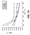
図7Aと7Bは、夫々が、従来のスパッタリング方法によって形成されたSiO2薄膜の屈曲率と、本発明によるネガティブ・スパッタ・イオン・ビーム源によって形成されたSiO2薄膜の屈曲率とに、異なった傾向があることを表す長時間経過した後のグラフを示す。図7Aと7Bに示されるように、従来のスパッタリング方法によって形成された酸化物薄膜は、長時間経過した後、屈曲率の大きな変化に見舞われる。一方、本発明における方法で形成された酸化物薄膜は、相当な時間経過後でも一定の屈曲率を示す。 7A and 7B differ in the bending rate of the SiO 2 thin film formed by the conventional sputtering method and the bending rate of the SiO 2 thin film formed by the negative sputtering ion beam source according to the present invention, respectively. The graph after a long time showing that there is a tendency is shown. As shown in FIGS. 7A and 7B, the oxide thin film formed by the conventional sputtering method suffers a large change in the bending rate after a long time. On the other hand, the oxide thin film formed by the method of the present invention exhibits a constant bending rate even after a considerable time has elapsed.
図8は、従来技術の方法で形成されたSiO2薄膜の屈曲率と、本発明による方法で形成されたSiO2薄膜の屈曲率との比較を図示したものである。屈曲率の変化は、632.8nmの波長に関して測定される。 FIG. 8 illustrates a comparison between the bending rate of the SiO 2 thin film formed by the method of the prior art and the bending rate of the SiO 2 thin film formed by the method of the present invention. The change in flexure is measured for a wavelength of 632.8 nm.
一般的に、SiO2のような酸化物薄膜は、蒸着完了後にエージング効果の影響を受ける。蒸着完了後の薄膜の屈曲率および厚さの変化を最小化するためには、高密度のフィルムであることが望ましい。上述のように、高密度の薄膜は、本発明の陰イオン源を利用することによって形成される。 In general, an oxide thin film such as SiO 2 is affected by an aging effect after deposition is completed. In order to minimize the change in the bending rate and thickness of the thin film after completion of the deposition, a high-density film is desirable. As described above, a high density thin film is formed by utilizing the anion source of the present invention.
酸素分圧は、SiO2蒸着工程において1つの重要な要因である。図9は、異なった酸素分圧状態下でのSiO2薄膜のエージング効果を表すグラフを示す。 The oxygen partial pressure is one important factor in the SiO 2 deposition process. FIG. 9 shows a graph representing the aging effect of the SiO 2 thin film under different oxygen partial pressure conditions.
図9は、様々な酸素分圧に関して、異なった出力状態でのネガティブ・スパッタ・イオン・ビーム源によって形成された、SiO2薄膜のエージング効果を表すグラフを示す。 FIG. 9 shows a graph representing the aging effect of SiO 2 thin films formed by negative sputter ion beam sources at different power conditions for various oxygen partial pressures.
図9に示されたように、酸素分圧は、アルゴン・ガスの供給に対する酸素ガスの割合で表されている。酸素分圧が上昇すると(即ち10%〜15%および20%)、SiO2薄膜の屈曲率は低下する。イオン・ビーム蒸着工程は、高酸化状態と高充填密度とを導くことが知られている。SiO2膜の吸光係数は、光学被膜に用いられるのに充分小さい(即ちk<3×10⁻³)。また、酸素分圧が上昇すると、蒸着率の減少が観測される。 As shown in FIG. 9, the oxygen partial pressure is expressed as a ratio of oxygen gas to argon gas supply. As the oxygen partial pressure increases (ie, 10% to 15% and 20%), the bending rate of the SiO 2 thin film decreases. It is known that the ion beam deposition process leads to a high oxidation state and a high packing density. The extinction coefficient of the SiO 2 film is small enough to be used for an optical coating (ie, k <3 × 10 −3 ). Moreover, when the oxygen partial pressure increases, a decrease in the deposition rate is observed.
出力の依存性もまた、高出力レジーム、中出力レジーム、低出力レジームの3つの異なる出力レジームで調査される。NSIB源において、基板での粒子の運動エネルギーは、カソード電圧の作用である。処理圧力が蒸着工程全体を通して同様に10−4〜10−2トルに留まるので、高出力状態であるほど高イオン・ビーム・エネルギー状態であると考えられる。圧力が無衝突移動を提供するのに充分な程低い場合、最も起こりうる陰イオン到達エネルギーは、カソード電圧と定義可能である。 Output dependency is also investigated in three different output regimes: high output regime, medium output regime, and low output regime. In an NSIB source, the kinetic energy of particles at the substrate is a function of the cathode voltage. Since the processing pressure similarly remains at 10 −4 to 10 −2 Torr throughout the deposition process, the higher the power output, the higher the ion beam energy state. If the pressure is low enough to provide collisionless movement, the most likely anion arrival energy can be defined as the cathode voltage.
図10Aは、屈曲率(n)に関するSiO2薄膜のエージング効果を表すグラフを示す。図10Bは、厚さ変化に関するSiO2薄膜のエージング効果を表すグラフを示す。 FIG. 10A shows a graph representing the aging effect of the SiO 2 thin film on the bending rate (n). FIG. 10B shows a graph representing the aging effect of the SiO 2 thin film with respect to thickness change.
図10Aと10Bに示されるように、屈曲率の変化は、異なった出力レジームでプロットされる。屈曲率の変化は、低蒸着率のため、低出力レジームにおいて3つの状態中最も小さい。 As shown in FIGS. 10A and 10B, the change in flexure is plotted with different output regimes. The change in flex rate is the smallest of the three states in the low power regime because of the low deposition rate.
屈曲率は、高表面移動によって、ある波長で温度と共に上昇する傾向にあることが報告されている。粒子のエネルギー性衝撃で、同様の結果が得られる。異なった出力設定とは関係なく、屈曲率の変化は、蒸着5日後よりも最初の5日の方が顕著に現れる。厚さの変化も同様の傾向にある。 It has been reported that the bending rate tends to increase with temperature at a certain wavelength due to high surface movement. Similar results are obtained with energetic impact of the particles. Regardless of the different output settings, the change in flexure appears more markedly on the first 5 days than on the 5th day after deposition. The change in thickness has a similar tendency.
図10Aと10Bにおいて、両方のプロットは、期間全体を通しての最大ポイントと最小ポイントとの間の変動を表している。変動の振幅は時間で減少する。屈曲率の全体の変化において、低出力状態が、他の状態より安定している。厚さ変化の場合、高パワー状態が、他の状態より安定している。データに示されたように、エージング効果は、酸化物薄膜の蒸着率に関連している。 In FIGS. 10A and 10B, both plots represent the variation between the maximum and minimum points throughout the period. The amplitude of variation decreases with time. The low output state is more stable than the other states in the overall change in the bending rate. In the case of thickness change, the high power state is more stable than the other states. As shown in the data, the aging effect is related to the deposition rate of the oxide thin film.
図11Aと11Bは、夫々が本発明のNSIB源によって形成されたSiO2薄膜の反射率データの1ヶ月間の計算値と測定値の比較を表したグラフを示し、図11Aが1日目で、11Bが30日目を示すグラフである。グラフに示されるように、1日目と30日目との間の変化はあまりない。また測定データは殆ど計算データと同じである。 FIGS. 11A and 11B are graphs showing comparisons between calculated values and measured values for one month of reflectance data of SiO 2 thin films formed by the NSIB source of the present invention, respectively, and FIG. 11B is a graph showing the 30th day. As shown in the graph, there is not much change between day 1 and day 30. The measurement data is almost the same as the calculation data.
図12は、供給されたカソード電圧の作用としてSiO2薄膜の蒸着率を表すグラフを示す。約1Kwでの蒸着率は、ほぼ7Å/秒である。 FIG. 12 shows a graph representing the deposition rate of the SiO 2 thin film as a function of the supplied cathode voltage. The deposition rate at about 1 Kw is about 7 liters / second.
上記データの傾向を以下のように説明可能である。酸化物薄膜の密度に直接関連する多孔率は、反射率プロットのパターンを通じて予想が可能である。反射率データからの薄膜の多孔率は、異なった波長レジームで検査可能である。 The trend of the data can be explained as follows. The porosity directly related to the density of the oxide thin film can be predicted through the pattern of the reflectance plot. The porosity of the thin film from the reflectance data can be examined with different wavelength regimes.
上記の図面に示されるように、計算値と測定値との間の一致性が高い程、高密度なSiO2薄膜であることを示す。一方、2つの値の一致性が低い程、より多孔な膜であることを示す。図11Aと11Bは、1ヶ月経過後のSiO2薄膜の多孔率データを示す。そのデータは、本測定で利用された薄膜が、1ヶ月後に高密度状態を保っていることを示す。 As shown in the above drawings, the higher the consistency between the calculated value and the measured value, the higher the density of the SiO 2 thin film. On the other hand, the lower the match between the two values, the more porous the film. 11A and 11B show the porosity data of the SiO2 thin film after one month. The data shows that the thin film used in this measurement remains in a high density state after one month.
蒸着率は、他の説明に利用可能である。本発明に採用された陰イオン源は、ターゲット表面上のCs層による表面イオン化をベースにしている。従って、産業レベルの高蒸着率状態において、Cs蒸気流量率が重要な役割を果たす。 The deposition rate can be used for other explanations. The anion source employed in the present invention is based on surface ionization with a Cs layer on the target surface. Therefore, the Cs vapor flow rate plays an important role in an industrial-level high deposition rate state.
図13Aと13Bは、本発明によるネガティブ・スパッタ・イオン・ビーム源によって形成された、酸化チタン(TiO2)薄膜の透過率、屈曲率、吸光係数を表すグラフを示す。 FIGS. 13A and 13B show graphs representing the transmittance, flexural modulus, and extinction coefficient of a titanium oxide (TiO 2 ) thin film formed by a negative sputter ion beam source according to the present invention.
高屈曲率を持つ酸化チタン薄膜は、殆どの応用に望ましい。通常、屈曲率は、高表面移動によって、ある波長で温度と共に上昇する。本発明におけるネガティブ・スパッタ・イオン・ビームで達成する粒子のエネルギー性衝撃は、結果として同様の表面移動をもたらす可能性がある。図13Aと13Bに示されるように、酸化チタン薄膜は、高屈曲率(即ちn>2.6)であり、低吸収係数(即ちk<0.0005)で、他の方法では絶対に得られない。 Titanium oxide thin films with a high bending rate are desirable for most applications. Usually, the bending rate increases with temperature at a certain wavelength due to high surface movement. The energetic bombardment of particles achieved with a negative sputter ion beam in the present invention can result in similar surface movement. As shown in FIGS. 13A and 13B, the titanium oxide thin film has a high bending rate (ie, n> 2.6), a low absorption coefficient (ie, k <0.0005), and is absolutely obtained by other methods. Absent.
上述のように、NSIB源を利用して蒸着された酸化物薄膜は、低表面粗度、低ウエット・エッチ率、長時間後の最小屈曲率変化等の望ましい特質を有している。酸化物薄膜の特質は、イオン・ビーム・エネルギーと酸素分圧に依存する。しかし、酸化物薄膜の屈曲率と厚さの変化は、比較的一定である。1ヶ月間を通しての屈曲率の変化は、屈曲率の値とは関係なく、殆どの場合2%よりも小さい。従来の工程において、蒸着5日後の変化は5%よりも大きい。エージング効果は、高蒸着率薄膜においてより激しいものである。 As described above, oxide thin films deposited using NSIB sources have desirable characteristics such as low surface roughness, low wet etch rate, and minimum flexural change after long periods of time. The nature of oxide thin films depends on ion beam energy and oxygen partial pressure. However, the change in the bending rate and thickness of the oxide thin film is relatively constant. The change in flexion rate throughout the month is almost less than 2%, regardless of the flex rate value. In the conventional process, the change after 5 days of deposition is greater than 5%. The aging effect is more severe in high deposition rate thin films.
本発明において、酸化物薄膜の特質はまた、異なった蒸着状態で調査される。総合結果は、望ましい酸化物薄膜が、高蒸着率状態でもCs流量率を制御することによって蒸着されることを示している。また、酸化物薄膜の特質は、陰イオンエネルギーの変化で変わる。これは、太陽電池等の幾つかの応用においての利点となり、そこでは粗面が平滑面よりも望ましい。 In the present invention, the characteristics of oxide thin films are also investigated in different deposition conditions. The overall results show that desirable oxide thin films are deposited by controlling the Cs flow rate even at high deposition rate conditions. In addition, the characteristics of oxide thin films change with changes in anion energy. This is an advantage in some applications, such as solar cells, where a rough surface is preferred over a smooth surface.
本発明のネガティブ・スパッタ・イオン・ビーム源を利用した酸化物薄膜の形成方法には、発明の精神と範囲を逸脱すること無く、様々な修正や変更が可能であることが当業者にとって自明である。従って、これらの修正や変更が、添付の請求の範囲とその同等の範囲内である場合、本発明はこれらを含むように意図している。 It is obvious to those skilled in the art that various modifications and changes can be made to the method for forming an oxide thin film using the negative sputtering ion beam source of the present invention without departing from the spirit and scope of the invention. is there. Accordingly, it is intended that the present invention cover these modifications and variations that come within the scope of the appended claims and their equivalents.
Claims (22)
仕事関数還元剤を処理チャンバ中の基板に対面するスパッタ・ターゲットの表面に導入する工程、
酸素ガスおよび不活性ガスを該処理チャンバに供給する工程、
該酸素ガスおよび該不活性ガスをイオン化することによって複数の電子を生成する工程、
該スパッタ・ターゲットから複数の陰荷電イオンを解離させる工程、ならびに
イオン化酸素ガスと反応した陰荷電イオンから、該基板上に該酸化物薄膜を形成する工程、
を包含する、方法。 A method for forming an oxide thin film, comprising:
Introducing a work function reducing agent to the surface of the sputter target facing the substrate in the processing chamber;
Supplying oxygen gas and inert gas to the processing chamber;
Generating a plurality of electrons by ionizing the oxygen gas and the inert gas;
Dissociating a plurality of negatively charged ions from the sputter target; and forming the oxide thin film on the substrate from negatively charged ions reacted with ionized oxygen gas;
Including the method.
処理チャンバ中の基板を事前スパッタリングして、該基板の表面を清浄化する工程、
該処理チャンバを排気して基底圧力を維持する工程、
仕事関数還元剤を該基板に対面するスパッタ・ターゲットの表面に導入する工程、
酸素ガスおよび不活性ガスを該処理チャンバに供給する工程、
該処理チャンバの処理圧力を維持する工程、
該酸素ガスおよび不活性ガスをイオン化することによって複数の電子を生成する工程、
該スパッタ・ターゲットの表面近隣に電子を閉じ込める工程、
該スパッタ・ターゲットから該複数の陰荷電イオンを解離させる工程、
該イオン化酸素ガスと反応した陰荷電イオンから該基板上に該酸化物薄膜を形成する工程、
を包含する、方法。 A method of forming an oxide thin film using a magnetron sputtering system,
Pre-sputtering a substrate in a processing chamber to clean the surface of the substrate;
Evacuating the processing chamber to maintain a base pressure;
Introducing a work function reducing agent to the surface of the sputtering target facing the substrate;
Supplying oxygen gas and inert gas to the processing chamber;
Maintaining a process pressure in the process chamber;
Generating a plurality of electrons by ionizing the oxygen gas and the inert gas;
Confining electrons near the surface of the sputter target;
Dissociating the plurality of negatively charged ions from the sputter target;
Forming the oxide thin film on the substrate from negatively charged ions reacted with the ionized oxygen gas;
Including the method.
Applications Claiming Priority (2)
| Application Number | Priority Date | Filing Date | Title |
|---|---|---|---|
| US10/300,783 US20040099525A1 (en) | 2002-11-21 | 2002-11-21 | Method of forming oxide thin films using negative sputter ion beam source |
| PCT/US2003/036791 WO2004049397A2 (en) | 2002-11-21 | 2003-11-18 | A method of forming an oxide thin films using negative sputter ion beam source |
Publications (1)
| Publication Number | Publication Date |
|---|---|
| JP2006507411A true JP2006507411A (en) | 2006-03-02 |
Family
ID=32324430
Family Applications (1)
| Application Number | Title | Priority Date | Filing Date |
|---|---|---|---|
| JP2004555480A Withdrawn JP2006507411A (en) | 2002-11-21 | 2003-11-18 | Method for forming oxide thin film using negative sputter ion beam source |
Country Status (4)
| Country | Link |
|---|---|
| US (1) | US20040099525A1 (en) |
| JP (1) | JP2006507411A (en) |
| AU (1) | AU2003291039A1 (en) |
| WO (1) | WO2004049397A2 (en) |
Families Citing this family (3)
| Publication number | Priority date | Publication date | Assignee | Title |
|---|---|---|---|---|
| GB2408399B (en) * | 2003-11-24 | 2007-01-10 | Nordiko Technical Services Ltd | Formation of a Dielectric on a Thin Metal Film Using an Ion Beam |
| JP2006283709A (en) * | 2005-04-01 | 2006-10-19 | Toyota Motor Corp | Control device for internal combustion engine |
| TW200741241A (en) * | 2006-04-17 | 2007-11-01 | Asia Optical Co Inc | Lens to reduce the stray light |
Family Cites Families (7)
| Publication number | Priority date | Publication date | Assignee | Title |
|---|---|---|---|---|
| US4022939A (en) * | 1975-12-18 | 1977-05-10 | Western Electric Company, Inc. | Synchronous shielding in vacuum deposition system |
| WO1980000504A1 (en) * | 1978-08-18 | 1980-03-20 | Nat Res Dev | Control of deposition of thin films |
| CA1155798A (en) * | 1981-03-30 | 1983-10-25 | Shmuel Maniv | Reactive deposition method and apparatus |
| US4428811A (en) * | 1983-04-04 | 1984-01-31 | Borg-Warner Corporation | Rapid rate reactive sputtering of a group IVb metal |
| US4828346A (en) * | 1985-10-08 | 1989-05-09 | The Boc Group, Inc. | Transparent article having high visible transmittance |
| US6383345B1 (en) * | 2000-10-13 | 2002-05-07 | Plasmion Corporation | Method of forming indium tin oxide thin film using magnetron negative ion sputter source |
| KR20030065810A (en) * | 2002-02-01 | 2003-08-09 | 필터레이 화이버 옵틱스 인코퍼레이티드 | Apparatus and method for fabricating optical coating |
-
2002
- 2002-11-21 US US10/300,783 patent/US20040099525A1/en not_active Abandoned
-
2003
- 2003-11-18 JP JP2004555480A patent/JP2006507411A/en not_active Withdrawn
- 2003-11-18 WO PCT/US2003/036791 patent/WO2004049397A2/en not_active Ceased
- 2003-11-18 AU AU2003291039A patent/AU2003291039A1/en not_active Abandoned
Also Published As
| Publication number | Publication date |
|---|---|
| WO2004049397A3 (en) | 2004-09-16 |
| AU2003291039A8 (en) | 2004-06-18 |
| US20040099525A1 (en) | 2004-05-27 |
| AU2003291039A1 (en) | 2004-06-18 |
| WO2004049397A2 (en) | 2004-06-10 |
Similar Documents
| Publication | Publication Date | Title |
|---|---|---|
| US5597622A (en) | Process for the production of a reflection-reducing coating on lenses | |
| EP0945523B1 (en) | Method for forming a thin film and apparatus for carrying out the method | |
| JP7676466B2 (en) | Method and apparatus for forming a low-grain layer on a substrate - Patents.com | |
| Vlček et al. | High-rate reactive high-power impulse magnetron sputtering of hard and optically transparent HfO2 films | |
| US20060023311A1 (en) | Method for obtaining a thin, stabilized fluorine-doped silica layer, resulting thin layer, and use thereof in ophthalmic optics | |
| JP2018513423A (en) | Coated optical object and method of manufacturing a coated optical object | |
| CN111926293A (en) | Optical device and method for manufacturing the same | |
| US9562283B2 (en) | Coating of optical substrates using closed field system | |
| EP1630248B1 (en) | Thin film forming method | |
| JP2006507411A (en) | Method for forming oxide thin film using negative sputter ion beam source | |
| Kim et al. | DC reactive magnetron sputtering with Ar ion-beam assistance for titanium oxide films | |
| Westwood | Reactive sputtering: introduction and general discussion | |
| JPH09148676A (en) | Semiconductor laser and method of manufacturing the same | |
| JP4613015B2 (en) | Film forming method and film forming apparatus | |
| Pulker | Plasma-and ion-assisted PVD technologies for the production of hard optical coatings | |
| KR100874867B1 (en) | Zirconium oxide film formation method | |
| JP4359674B2 (en) | High-speed film formation method of photocatalytic titanium oxide film | |
| NL2033303B1 (en) | Method for manufacturing an aluminium oxide optical waveguide, and aluminium oxide optical waveguide | |
| KR101907143B1 (en) | a fabricating method for anti-reflection film with an excellent performance and a anti-reflection film fabricated thereof | |
| NL2033304B1 (en) | Method for manufacturing an aluminium nitride optical waveguide, and aluminium nitride optical waveguide | |
| KR100399763B1 (en) | Method for manufacturing ZnO layer using sputtering deposition | |
| Uetani et al. | Ultra thin TiN films prepared by an advanced ion-plating method | |
| Paik | The stability of SiO2 films prepared using a magnetron sputter type negative ion source (MSNIS) | |
| JP2008062561A (en) | Method for producing article provided with hydrophilic laminated film, and article provided with hydrophilic laminated film | |
| JPH10183332A (en) | Production of optical thin film and device therefor |
Legal Events
| Date | Code | Title | Description |
|---|---|---|---|
| A300 | Application deemed to be withdrawn because no request for examination was validly filed |
Free format text: JAPANESE INTERMEDIATE CODE: A300 Effective date: 20070206 |