JP2006339514A - Semiconductor device and manufacturing method thereof - Google Patents
Semiconductor device and manufacturing method thereof Download PDFInfo
- Publication number
- JP2006339514A JP2006339514A JP2005164210A JP2005164210A JP2006339514A JP 2006339514 A JP2006339514 A JP 2006339514A JP 2005164210 A JP2005164210 A JP 2005164210A JP 2005164210 A JP2005164210 A JP 2005164210A JP 2006339514 A JP2006339514 A JP 2006339514A
- Authority
- JP
- Japan
- Prior art keywords
- region
- insulating film
- gate electrode
- gate
- mask
- Prior art date
- Legal status (The legal status is an assumption and is not a legal conclusion. Google has not performed a legal analysis and makes no representation as to the accuracy of the status listed.)
- Granted
Links
Images


Classifications
-
- H—ELECTRICITY
- H10—SEMICONDUCTOR DEVICES; ELECTRIC SOLID-STATE DEVICES NOT OTHERWISE PROVIDED FOR
- H10D—INORGANIC ELECTRIC SEMICONDUCTOR DEVICES
- H10D30/00—Field-effect transistors [FET]
- H10D30/60—Insulated-gate field-effect transistors [IGFET]
- H10D30/62—Fin field-effect transistors [FinFET]
-
- H—ELECTRICITY
- H10—SEMICONDUCTOR DEVICES; ELECTRIC SOLID-STATE DEVICES NOT OTHERWISE PROVIDED FOR
- H10D—INORGANIC ELECTRIC SEMICONDUCTOR DEVICES
- H10D30/00—Field-effect transistors [FET]
- H10D30/01—Manufacture or treatment
- H10D30/021—Manufacture or treatment of FETs having insulated gates [IGFET]
- H10D30/024—Manufacture or treatment of FETs having insulated gates [IGFET] of fin field-effect transistors [FinFET]
- H10D30/0243—Manufacture or treatment of FETs having insulated gates [IGFET] of fin field-effect transistors [FinFET] using dummy structures having essentially the same shapes as the semiconductor bodies, e.g. to provide stability
-
- H—ELECTRICITY
- H10—SEMICONDUCTOR DEVICES; ELECTRIC SOLID-STATE DEVICES NOT OTHERWISE PROVIDED FOR
- H10D—INORGANIC ELECTRIC SEMICONDUCTOR DEVICES
- H10D84/00—Integrated devices formed in or on semiconductor substrates that comprise only semiconducting layers, e.g. on Si wafers or on GaAs-on-Si wafers
- H10D84/01—Manufacture or treatment
- H10D84/0123—Integrating together multiple components covered by H10D12/00 or H10D30/00, e.g. integrating multiple IGBTs
- H10D84/0126—Integrating together multiple components covered by H10D12/00 or H10D30/00, e.g. integrating multiple IGBTs the components including insulated gates, e.g. IGFETs
- H10D84/0158—Integrating together multiple components covered by H10D12/00 or H10D30/00, e.g. integrating multiple IGBTs the components including insulated gates, e.g. IGFETs the components including FinFETs
-
- H—ELECTRICITY
- H10—SEMICONDUCTOR DEVICES; ELECTRIC SOLID-STATE DEVICES NOT OTHERWISE PROVIDED FOR
- H10D—INORGANIC ELECTRIC SEMICONDUCTOR DEVICES
- H10D84/00—Integrated devices formed in or on semiconductor substrates that comprise only semiconducting layers, e.g. on Si wafers or on GaAs-on-Si wafers
- H10D84/01—Manufacture or treatment
- H10D84/02—Manufacture or treatment characterised by using material-based technologies
- H10D84/03—Manufacture or treatment characterised by using material-based technologies using Group IV technology, e.g. silicon technology or silicon-carbide [SiC] technology
- H10D84/038—Manufacture or treatment characterised by using material-based technologies using Group IV technology, e.g. silicon technology or silicon-carbide [SiC] technology using silicon technology, e.g. SiGe
-
- H—ELECTRICITY
- H10—SEMICONDUCTOR DEVICES; ELECTRIC SOLID-STATE DEVICES NOT OTHERWISE PROVIDED FOR
- H10D—INORGANIC ELECTRIC SEMICONDUCTOR DEVICES
- H10D84/00—Integrated devices formed in or on semiconductor substrates that comprise only semiconducting layers, e.g. on Si wafers or on GaAs-on-Si wafers
- H10D84/80—Integrated devices formed in or on semiconductor substrates that comprise only semiconducting layers, e.g. on Si wafers or on GaAs-on-Si wafers characterised by the integration of at least one component covered by groups H10D12/00 or H10D30/00, e.g. integration of IGFETs
- H10D84/82—Integrated devices formed in or on semiconductor substrates that comprise only semiconducting layers, e.g. on Si wafers or on GaAs-on-Si wafers characterised by the integration of at least one component covered by groups H10D12/00 or H10D30/00, e.g. integration of IGFETs of only field-effect components
- H10D84/83—Integrated devices formed in or on semiconductor substrates that comprise only semiconducting layers, e.g. on Si wafers or on GaAs-on-Si wafers characterised by the integration of at least one component covered by groups H10D12/00 or H10D30/00, e.g. integration of IGFETs of only field-effect components of only insulated-gate FETs [IGFET]
- H10D84/834—Integrated devices formed in or on semiconductor substrates that comprise only semiconducting layers, e.g. on Si wafers or on GaAs-on-Si wafers characterised by the integration of at least one component covered by groups H10D12/00 or H10D30/00, e.g. integration of IGFETs of only field-effect components of only insulated-gate FETs [IGFET] comprising FinFETs
-
- H—ELECTRICITY
- H01—ELECTRIC ELEMENTS
- H01L—SEMICONDUCTOR DEVICES NOT COVERED BY CLASS H10
- H01L21/00—Processes or apparatus adapted for the manufacture or treatment of semiconductor or solid state devices or of parts thereof
- H01L21/02—Manufacture or treatment of semiconductor devices or of parts thereof
- H01L21/04—Manufacture or treatment of semiconductor devices or of parts thereof the devices having potential barriers, e.g. a PN junction, depletion layer or carrier concentration layer
- H01L21/18—Manufacture or treatment of semiconductor devices or of parts thereof the devices having potential barriers, e.g. a PN junction, depletion layer or carrier concentration layer the devices having semiconductor bodies comprising elements of Group IV of the Periodic Table or AIIIBV compounds with or without impurities, e.g. doping materials
- H01L21/28—Manufacture of electrodes on semiconductor bodies using processes or apparatus not provided for in groups H01L21/20 - H01L21/268
- H01L21/28008—Making conductor-insulator-semiconductor electrodes
- H01L21/28017—Making conductor-insulator-semiconductor electrodes the insulator being formed after the semiconductor body, the semiconductor being silicon
- H01L21/28026—Making conductor-insulator-semiconductor electrodes the insulator being formed after the semiconductor body, the semiconductor being silicon characterised by the conductor
- H01L21/28097—Making conductor-insulator-semiconductor electrodes the insulator being formed after the semiconductor body, the semiconductor being silicon characterised by the conductor the final conductor layer next to the insulator being a metallic silicide
-
- H—ELECTRICITY
- H10—SEMICONDUCTOR DEVICES; ELECTRIC SOLID-STATE DEVICES NOT OTHERWISE PROVIDED FOR
- H10D—INORGANIC ELECTRIC SEMICONDUCTOR DEVICES
- H10D30/00—Field-effect transistors [FET]
- H10D30/60—Insulated-gate field-effect transistors [IGFET]
- H10D30/62—Fin field-effect transistors [FinFET]
- H10D30/6211—Fin field-effect transistors [FinFET] having fin-shaped semiconductor bodies integral with the bulk semiconductor substrates
Landscapes
- Metal-Oxide And Bipolar Metal-Oxide Semiconductor Integrated Circuits (AREA)
- Insulated Gate Type Field-Effect Transistor (AREA)
- Thin Film Transistor (AREA)
- Electrodes Of Semiconductors (AREA)
- Element Separation (AREA)
- Semiconductor Memories (AREA)
Abstract
【課題】 本発明は、微細な回路パターンを形成することができる半導体装置及びその製造方法を提供することを目的とする。
【解決手段】 第2の領域20に形成されたマスク材50にエッチングを行ってこれを除去するステップと、第1の凸部10Bのうち、対向する1組の両側面に第1のゲート絶縁膜100B及び100Cを形成すると共に、第2の凸部10Aの上面に第2のゲート絶縁膜100Aを形成するステップと、素子分離絶縁膜70、マスク材50及び第2のゲート絶縁膜100A上に第1のゲート電極材110を堆積するステップと、第1の領域30に形成されたマスク材50と、第2の領域20に形成された素子分離絶縁膜70とをストッパとして、第1のゲート電極材110を平坦化するステップとを備えることを特徴とする。
【選択図】 図6An object of the present invention is to provide a semiconductor device capable of forming a fine circuit pattern and a manufacturing method thereof.
A step of etching and removing a mask material 50 formed in a second region 20 and a first gate insulation on a pair of opposing side surfaces of a first convex portion 10B. The steps of forming the films 100B and 100C and forming the second gate insulating film 100A on the upper surface of the second protrusion 10A, the element isolation insulating film 70, the mask material 50, and the second gate insulating film 100A The first gate electrode material 110 is deposited, the mask material 50 formed in the first region 30 and the element isolation insulating film 70 formed in the second region 20 as stoppers. A step of planarizing the electrode material 110.
[Selection] Figure 6
Description
本発明は、半導体装置及びその製造方法に関する。 The present invention relates to a semiconductor device and a manufacturing method thereof.
近年、いわゆる縦型ダブルゲート構造のMOSFETが開発されており、なかでも半導体層がFin状に形成されたMOSFETは、FinFETと呼ばれている。かかるFinFETは、製造コストが低く、カットオフ特性が良好なデバイスであるため、次世代のトランジスタ構造として有望視されている。 In recent years, a MOSFET having a so-called vertical double gate structure has been developed, and a MOSFET in which a semiconductor layer is formed in a Fin shape is called a FinFET. Such FinFETs are promising as next-generation transistor structures because of their low manufacturing cost and good cut-off characteristics.
しかし、ゲート閾値電圧が高いデバイスの実現や、アナログデバイスの対応には、FinFETよりプレーナ型(平面型)MOSFETの方が優れている。このため、実際のLSIでは、プレーナ型MOSFETとFinFETとを混載することが必要とされ、これらプレーナ型MOSFETとFinFETとを混載するための簡易な製造プロセスが求められている。 However, the planar (planar) MOSFET is superior to the FinFET for realizing a device having a high gate threshold voltage and for supporting an analog device. For this reason, in an actual LSI, it is necessary to mix planar MOSFETs and FinFETs, and a simple manufacturing process for mounting these planar MOSFETs and FinFETs is required.
しかし、プレーナ型MOSFETとFinFETとを混載しようとすると、ゲート電極材を堆積した際に、当該ゲート電極材の表面に凹凸が形成され、これにより微細なゲートパターンを形成することができないという問題があった。 However, when the planar type MOSFET and the FinFET are mixedly mounted, when the gate electrode material is deposited, irregularities are formed on the surface of the gate electrode material, thereby making it impossible to form a fine gate pattern. there were.
以下、プレーナ型MOSFETとFinFETとを混載する半導体装置の製造方法に関する文献名を記載する。
本発明は、微細な回路パターンを形成することができる半導体装置及びその製造方法を提供することを目的とする。 An object of this invention is to provide the semiconductor device which can form a fine circuit pattern, and its manufacturing method.
本発明の一態様による半導体装置の製造方法は、
半導体基板上にマスク材を堆積するステップと、
前記マスク材にパターニングを行い、さらに前記半導体基板の表面部分にエッチングを行って溝を形成することにより、第1の領域には第1の凸部を形成すると共に、第2の領域には前記第1の凸部より広い幅を有する第2の凸部を形成するステップと、
前記溝を素子分離絶縁膜で埋め込むステップと、
前記第1の領域に形成された前記素子分離絶縁膜にエッチングを行うことにより、所定量除去するステップと、
前記第2の領域に形成された前記マスク材にエッチングを行ってこれを除去するステップと、
前記第1の凸部のうち、対向する1組の両側面に第1のゲート絶縁膜を形成すると共に、前記第2の凸部の上面に第2のゲート絶縁膜を形成するステップと、
前記素子分離絶縁膜、前記マスク材及び前記第2のゲート絶縁膜上に第1のゲート電極材を堆積するステップと、
前記第1の領域に形成された前記マスク材と、前記第2の領域に形成された前記素子分離絶縁膜とをストッパとして、前記第1のゲート電極材を平坦化するステップと、
前記マスク材、前記第1のゲート電極材及び前記素子分離絶縁膜上に第2のゲート電極材を堆積するステップと、
前記第1及び第2のゲート電極材にパターニングを行うことにより、前記第1の領域に第1のゲート電極を形成すると共に、前記第2の領域に第2のゲート電極を形成するステップと
を備えることを特徴とする。
A method for manufacturing a semiconductor device according to one embodiment of the present invention includes:
Depositing a mask material on a semiconductor substrate;
By patterning the mask material and further etching the surface portion of the semiconductor substrate to form a groove, the first region is formed in the first region, and the second region is Forming a second protrusion having a width wider than the first protrusion;
Filling the trench with an element isolation insulating film;
Removing a predetermined amount by etching the element isolation insulating film formed in the first region;
Etching the mask material formed in the second region to remove it;
Forming a first gate insulating film on a pair of opposing side surfaces of the first convex portion, and forming a second gate insulating film on the upper surface of the second convex portion;
Depositing a first gate electrode material on the element isolation insulating film, the mask material, and the second gate insulating film;
Planarizing the first gate electrode material using the mask material formed in the first region and the element isolation insulating film formed in the second region as stoppers;
Depositing a second gate electrode material on the mask material, the first gate electrode material and the element isolation insulating film;
Patterning the first and second gate electrode materials to form a first gate electrode in the first region and forming a second gate electrode in the second region; It is characterized by providing.
また本発明の一態様による半導体装置の製造方法は、
半導体基板上にマスク材を堆積するステップと、
前記マスク材にパターニングを行い、さらに前記半導体基板の表面部分にエッチングを行って溝を形成することにより、第1の領域には第1の凸部を形成すると共に、第2の領域には前記第1の凸部より広い幅を有する第2の凸部を形成するステップと、
前記溝を素子分離絶縁膜で埋め込むステップと、
前記第1の領域に形成された前記素子分離絶縁膜にエッチングを行うことにより、所定量除去するステップと、
前記第1の凸部のうち、対向する1組の両側面に第1のゲート絶縁膜を形成するステップと、
前記マスク材及び前記素子分離絶縁膜上に第1のゲート電極材を堆積するステップと、
前記マスク材及び前記素子分離絶縁膜をストッパとして、前記第1のゲート電極材を平坦化するステップと、
前記第2の領域に形成された前記マスク材にエッチングを行ってこれを除去するステップと、
前記第1及び第2の領域に第2のゲート絶縁膜を形成するステップと、
前記第2のゲート絶縁膜を形成する際に前記第1の領域に形成された前記第2のゲート絶縁膜を除去するステップと
を備えることを特徴とする。
A method for manufacturing a semiconductor device according to one embodiment of the present invention includes:
Depositing a mask material on a semiconductor substrate;
By patterning the mask material and further etching the surface portion of the semiconductor substrate to form a groove, the first region is formed in the first region, and the second region is Forming a second protrusion having a width wider than the first protrusion;
Filling the trench with an element isolation insulating film;
Removing a predetermined amount by etching the element isolation insulating film formed in the first region;
Forming a first gate insulating film on a pair of opposing side surfaces of the first convex portion; and
Depositing a first gate electrode material on the mask material and the element isolation insulating film;
Planarizing the first gate electrode material using the mask material and the element isolation insulating film as a stopper;
Etching the mask material formed in the second region to remove it;
Forming a second gate insulating film in the first and second regions;
Removing the second gate insulating film formed in the first region when forming the second gate insulating film.
また本発明の一態様による半導体装置の製造方法は、
表面の面方位が(110)である半導体基板上に、<112>方向に沿って、前記<112>方向と直交する方向に凹凸が形成されたパターンを有するマスクを形成するステップと、
前記マスクを用いて、前記半導体基板に面方位依存性を有するエッチングを行って、所定の深さだけ除去すると共に、前記マスクの凸部の下側に位置する前記半導体基板をも除去することにより、側面の面方位が(111)である凸部を形成するステップと
を備えることを特徴とする。
A method for manufacturing a semiconductor device according to one embodiment of the present invention includes:
Forming a mask having a pattern in which irregularities are formed in a direction perpendicular to the <112> direction along a <112> direction on a semiconductor substrate having a surface orientation of (110);
Etching having a plane orientation dependency is performed on the semiconductor substrate using the mask to remove the semiconductor substrate by a predetermined depth and also to remove the semiconductor substrate located below the convex portion of the mask. And a step of forming a convex portion whose side surface orientation is (111).
また本発明の一態様による半導体装置は、
表面の面方位が(110)である半導体基板の表面部分であって、かつ第1の領域に形成された凸部と、
前記凸部の側面のうち、対向する一組の両側面であって、かつ面方位が(111)である側面に、第1のゲート絶縁膜を介して形成された第1のゲート電極と、
前記凸部内において、前記第1のゲート電極が形成されていない側面側であって、面方位が(111)である前記対向する一組の両側面の間に形成される第1のチャネル領域の両側に、それぞれ形成された第1のソース領域及び第1のドレイン領域とを有するNチャネル型トランジスタと
前記半導体基板の表面上であって、かつ第2の領域に第2のゲート絶縁膜を介して形成された第2のゲート電極と、
前記半導体基板のうち前記第2の領域の表面部分において、前記第2のゲート電極の下方に形成される第2のチャネル領域の両側に、それぞれ形成された第2のソース領域及び第2のドレイン領域とを有するPチャネル型トランジスタと
を備えることを特徴とする。
A semiconductor device according to one embodiment of the present invention includes:
A surface portion of a semiconductor substrate having a surface orientation of (110) and a convex portion formed in the first region;
A first gate electrode formed on a side surface of the pair of opposing side surfaces of the convex portion and having a surface orientation of (111) via a first gate insulating film;
In the convex portion, the first channel region is formed on the side surface where the first gate electrode is not formed and between the pair of opposite side surfaces having a plane orientation of (111). An N-channel transistor having a first source region and a first drain region formed on both sides, and a surface of the semiconductor substrate, and a second gate insulating film on the second region A second gate electrode formed by
A second source region and a second drain respectively formed on both sides of a second channel region formed below the second gate electrode in the surface portion of the second region of the semiconductor substrate. And a p-channel transistor having a region.
本発明は、微細な回路パターンを形成することができる半導体装置及びその製造方法を提供することを目的とする。 An object of this invention is to provide the semiconductor device which can form a fine circuit pattern, and its manufacturing method.
以下、本発明の実施の形態について図面を参照して説明する。 Hereinafter, embodiments of the present invention will be described with reference to the drawings.
(1)第1の実施の形態
図1〜図9に、本発明の第1の実施の形態による半導体装置の製造方法を示す。なお、図1(a)〜図9(a)は、半導体基板10上のプレーナ型MOSFET領域(すなわち第2の領域)20にプレーナ型MOSFETを形成する場合を示し、図1(b)〜図9(b)は、半導体基板10上のFinFET領域(すなわち第1の領域)30にFinFETを形成する場合を示す。
(1) First Embodiment FIGS. 1 to 9 show a method for manufacturing a semiconductor device according to a first embodiment of the present invention. 1A to 9A show the case where a planar MOSFET is formed in the planar MOSFET region (that is, the second region) 20 on the
図1(a)及び(b)に示すように、半導体基板10上にシリコン酸化(SiO2)膜40を2nm程度形成した後、例えばシリコン窒化(SiN)膜からなるマスク材50を100nm程度堆積する。なお、マスク材50としては、シリコン窒化(SiN)膜に限らず、例えばシリコン酸化膜などの他の絶縁膜を用いることも可能である。
As shown in FIGS. 1A and 1B, after a silicon oxide (SiO 2 )
リソグラフィ及びRIEによって、マスク材50及びシリコン酸化膜40に順次パターニングを行う。さらにマスク材50をマスクとして、半導体基板10にエッチングを行うことにより、半導体基板10の表面からの深さが200nm程度の素子分離溝60を形成すると共に、プレーナ型MOSFET領域20には凸部10Aを形成し、FinFET領域30にはフィン10Bを形成する。
The
高密度プラズマ(High Density Plasma:HDP)CVD法を用いて、素子分離溝60を埋め込むように、半導体基板10及びマスク材50の全面に、例えばシリコン酸化膜からなる素子分離絶縁膜70を堆積する。マスク材50をストッパとして、CMP法によって素子分離絶縁膜70を平坦化することにより、マスク材50の上面を露出させる。
Using a high density plasma (HDP) CVD method, an element
図2(a)及び(b)に示すように、マスク材50及び素子分離絶縁膜70上にフォトレジストを塗布し、露光及び現像を行うことにより、半導体基板10のうちFinFET領域30が開口するパターンを有するレジストマスク80を形成し、プレーナ型MOSFET領域20をレジストマスク80で覆う。
As shown in FIGS. 2A and 2B, a
マスク材50及びレジストマスク80をマスクとして、RIEによって、FinFET領域30に形成された素子分離絶縁膜70にエッチングを行うことにより、素子分離絶縁膜70の膜厚を100nm程度にする。なお、RIEではなく、フッ酸(HF)を用いたウエットエッチングを行っても良い。
Using the
図3(a)及び(b)に示すように、レジストマスク80を除去した後、さらにマスク材50及び素子分離絶縁膜70上にフォトレジストを塗布し、露光及び現像を行うことにより、半導体基板10のうちプレーナ型MOSFET領域20が開口するパターンを有するレジストマスク90を形成し、FinFET領域30をレジストマスク90で覆う。
As shown in FIGS. 3A and 3B, after removing the
レジストマスク90をマスクとして、RIEによって、プレーナ型MOSFET領域20に形成されたマスク材50を除去した後、さらにフッ酸(HF)を用いたウエットエッチングによって、プレーナ型MOSFET20に形成されたシリコン酸化膜40を除去する。
After removing the
その際、素子分離絶縁膜70の高さが、半導体基板10のうち、プレーナ型MOSFET領域20の凸部10Aの表面を基準として70nm程度になるように、プロセス条件を調整した上でエッチングを行う。これにより、素子分離絶縁膜70の表面部分にエッチングが行われることを抑制し、素子分離絶縁膜70及びマスク材50それぞれの上面の高さを略同一にすることができる。
At that time, etching is performed after adjusting the process conditions so that the height of the element
図4(a)及び(b)に示すように、レジストマスク90を除去した後、半導体基板10のうち、プレーナ型MOSFET領域20の凸部10Aの表面上に、例えばシリコン酸窒化(SiON)膜からなるゲート絶縁膜100Aを1nm程度形成する。
4A and 4B, after removing the resist
これと共に、FinFET領域30のフィン10Bの対向する一組の両側面に、それぞれ例えばシリコン酸窒化(SiON)膜からなるゲート絶縁膜100B及び100Cを1nm程度形成する。
At the same time,
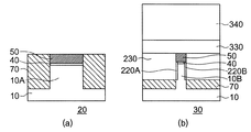
図5(a)及び(b)に示すように、CVD法などによって、1層目として、例えばポリシリコンからなるゲート電極材110を300nm程度堆積する。図6(a)及び(b)に示すように、プレーナ型MOSFET領域20の素子分離絶縁膜70と、FinFET領域30のマスク材50とをストッパとして、CMP法によって、ゲート電極材110を平坦化する。この場合、プレーナ型MOSFET領域20及びFinFET領域30の全面にわたって、ゲート電極材110を平坦化することができる。
As shown in FIGS. 5A and 5B, a
図7(a)及び(b)に示すように、CVD法などによって、2層目として、例えばポリシリコンからなるゲート電極材120を堆積する。図8(a)及び(b)に示すように、リソグラフィ及びRIEによって、ゲート電極材110及び120にパターニングを行うことにより、ゲートパターンを形成する。
As shown in FIGS. 7A and 7B, a
なお、この場合、いわゆるサイドウォール・パターン・トランスファー・プロセスを用いてゲートパターンを形成しても良い。このサイドウォール・パターン・トランスファー・プロセスとは、まずゲート電極材120上にダミーパターンを形成し、当該ダミーパターンの側面に側壁絶縁膜(サイドウォール)を形成する。そして、ダミーパターンを除去した後、側壁絶縁膜をマスクとして、ゲート電極材110及び120にパターニングを行うことにより、ゲートパターンを形成する方法である。
In this case, the gate pattern may be formed by using a so-called sidewall pattern transfer process. In this sidewall pattern transfer process, first, a dummy pattern is formed on the
その後、ゲート電極材110及び120からなるゲート電極の側面に側壁絶縁膜(図示せず)を形成する。図9(a)及び(b)に示すように、イオン注入によって、半導体基板10のうち、プレーナ型MOSFET領域20の凸部10Aの表面部分に、ソース領域130及びドレイン領域(図示せず)を形成し、FinFET領域30のフィン10Bに、ソース領域140及びドレイン領域(図示せず)を形成する。なお、FinFET領域30のフィン10Bへのイオン注入には、斜めイオン注入法やプラズマドーピング法を使用すれば良い。
Thereafter, a sidewall insulating film (not shown) is formed on the side surface of the gate electrode made of the
そして、シリサイド膜(図示せず)を形成した後、図示しない層間絶縁膜及びコンタクトプラグを順次形成して配線を行うことにより、プレーナ型MOSFETとFinFETとを混載した半導体装置を形成する。 Then, after forming a silicide film (not shown), an interlayer insulating film and a contact plug (not shown) are sequentially formed and wiring is performed, thereby forming a semiconductor device in which a planar MOSFET and a FinFET are mixedly mounted.
このように本実施の形態によれば、プレーナ型MOSFETとFinFETとを混載した半導体装置を簡易なプロセスで製造することができる。特に、プレーナ型MOSFET領域20及びFinFET領域30の全面にわたって、ゲート電極材120の表面を平坦化することができ、これにより微細なゲートパターンを形成することができる。
Thus, according to this embodiment, a semiconductor device in which a planar MOSFET and a FinFET are mixedly mounted can be manufactured by a simple process. In particular, the surface of the
すなわち、ゲート電極材120の表面を平坦化することができれば、リソグラフィのDOP(Depth of Focus:焦点深度)に対する要求を緩和することができ、よって解像度(形成することが可能な最小線幅)を向上させて、微細なゲートパターンを形成することができる。
That is, if the surface of the
また、ゲート電極材120の表面を平坦化することができれば、サイドウォール・パターン・トランスファー・プロセスを用いることができる。このサイドウォール・パターン・トランスファー・プロセスによれば、リソグラフィによっては形成することができない程度の狭い幅すなわち微細で、かつLER(Line Edge Roughness)すなわち凹凸が小さい(幅のばらつきが小さい均一な)ゲートパターンを形成することができる。
If the surface of the
なお、CMP法によって素子分離絶縁膜70を平坦化し、素子分離絶縁膜70及びマスク材50それぞれの上面の高さを略同一にしたこと(図1)、CMP法によってゲート電極材110を平坦化したこと(図6)、及びゲート電極を2層構造にしたことにより、プレーナ型MOSFET領域20のゲート電極材110及び120の基板深さ方向における厚さと、FinFET領域30(特にフィン10Bの両側面の近傍付近)のゲート電極材110及び120の基板深さ方向における厚さとの差は、素子分離絶縁膜70の上面がマスク材50の上面の高さより低く、かつゲート電極を平坦化しない場合と比較して小さい。
Note that the element
これにより、FinFET領域30のゲート電極材110及び120にパターニングを行う際、プレーナ型MOSFET領域20のゲート絶縁膜100Aにオーバーエッチングを行う時間を短縮することができる。従って、ゲート絶縁膜100Aに対するオーバーエッチング量を低減することができ、当該ゲート絶縁膜100Aの信頼性を向上させることができる。
Thereby, when patterning is performed on the
(2)第2の実施の形態
図10〜図12に、本発明の第2の実施の形態による半導体装置の製造方法を示す。なお、第1の実施の形態の図1〜図9における工程は、第2の実施の形態と同一であるため、説明を省略する。
(2) Second Embodiment FIGS. 10 to 12 show a method for manufacturing a semiconductor device according to a second embodiment of the present invention. In addition, since the process in FIGS. 1-9 of 1st Embodiment is the same as 2nd Embodiment, description is abbreviate | omitted.
但し、本実施の形態の場合、ゲート電極材110及び120からなるゲート電極は、後に除去されるダミーゲート電極であり、また同様に、ゲート絶縁膜100A〜100Cも、後に除去されるダミーゲート絶縁膜であり、これらの点について、第1の実施の形態と相違する。
However, in this embodiment, the gate electrode made of the
図10(a)及び(b)に示すように、高密度プラズマCVD法を用いて、例えばシリコン酸化膜からなる層間絶縁膜150を堆積した後、CMP法によってこの層間絶縁膜150を平坦化することにより、ゲート電極材120の上面を露出させる。
As shown in FIGS. 10A and 10B, after an
図11(a)及び(b)に示すように、RIEによって、ゲート電極材110及び120からなるダミーゲート電極を除去する。なお、この場合、RIEではなく、ウエットエッチングやCDE(Chemical Dry Etching)を用いても良い。
As shown in FIGS. 11A and 11B, the dummy gate electrode made of the
図12(a)及び(b)に示すように、ダミーゲート絶縁膜であるゲート絶縁膜100A〜100Cを除去した後、例えば高誘電率膜からなるゲート絶縁膜160A〜160Cを形成する。続いて、CVD法などによって、金属からなるメタルゲート電極材170を全面に堆積した後、層間絶縁膜150をストッパとして、CMP法によって、メタルゲート電極材170を平坦化することにより、メタルゲート電極を形成する。
As shown in FIGS. 12A and 12B, after the
これ以降、第1の実施の形態と同一の工程を実行することにより、プレーナ型MOSFETとFinFETとを混載した半導体装置を製造する。 Thereafter, the same process as that of the first embodiment is performed to manufacture a semiconductor device in which a planar type MOSFET and a FinFET are mixedly mounted.
このように本実施の形態によれば、第1の実施の形態と同様に、プレーナ型MOSFETとFinFETとを混載した半導体装置を簡易なプロセスで製造することができる。特に、プレーナ型MOSFET領域20及びFinFET領域30の全面にわたって、ゲート電極材120の表面を平坦化することができ、これにより微細なゲートパターンを形成することができる。
As described above, according to the present embodiment, a semiconductor device in which a planar MOSFET and a FinFET are mixedly mounted can be manufactured by a simple process, as in the first embodiment. In particular, the surface of the
また、第1の実施の形態と同様に、ダミーゲート絶縁膜であるゲート絶縁膜100Aに対するオーバーエッチング量を低減することができ、これにより半導体基板10の凸部10Aにオーバーエッチングを行うことを防止することができる。
In addition, as in the first embodiment, the amount of overetching with respect to the
さらに、上述したように、プレーナ型MOSFET領域20及びFinFET領域30の全面にわたって、ダミーゲート電極であるゲート電極材120の表面を平坦化することができるため、本実施の形態のように、いわゆるダマシンプロセスを行うことが可能になる。
Furthermore, as described above, since the surface of the
さらに、本実施の形態によれば、高い温度の熱処理工程を行って、ソース領域130及び140並びにドレイン領域(図示せず)を形成した後に、メタルゲート電極材170からなるメタルゲート電極を形成することができ、これによりゲート絶縁膜160A〜160Cの耐圧や信頼性を向上させることができる。
Furthermore, according to the present embodiment, a high temperature heat treatment step is performed to form the
さらに、メタルゲート電極材170の仕事関数(電子を外側に取り出すのに必要な最小エネルギー)を変化させれば、ゲート閾値電圧を調整することができる。 Furthermore, the gate threshold voltage can be adjusted by changing the work function of the metal gate electrode material 170 (minimum energy required to extract electrons to the outside).
なお上述の第2の実施の形態は一例であって、本発明を限定するものではない。例えばダミーゲート電極であるゲート電極材110及び120の全てをメタルゲート電極材170に置き換えるのではなく、ゲート電極材110及び120の一部のみをメタルゲート電極材170に置き換えても良い。具体的には、FinFET領域30のゲート電極材110及び120のみをメタルゲート電極材170に置き換え、プレーナ型MOSFET20のゲート電極材110及び120は置き換えなくても良い。
Note that the second embodiment described above is merely an example, and does not limit the present invention. For example, not all of the
(3)第3の実施の形態
図13に、本発明の第3の実施の形態による半導体装置の製造方法を示す。なお、第1の実施の形態の図1〜図9における工程と、第2の実施の形態の図10における工程は、第3の実施の形態と同一であるため、説明を省略する。
(3) Third Embodiment FIG. 13 shows a method for manufacturing a semiconductor device according to a third embodiment of the present invention. Note that the steps in FIGS. 1 to 9 of the first embodiment and the steps in FIG. 10 of the second embodiment are the same as those in the third embodiment, and a description thereof will be omitted.
図13(a)及び(b)に示すように、例えばポリシリコンからなるゲート電極材120及び層間絶縁膜150の全面に、例えばニッケルなどのシリサイド材料を堆積する。そして、熱処理工程を行って、ゲート電極材110及び120とシリサイド材料とを完全に反応させてシリサイド化した後、未反応のシリサイド材料をウエットエッチングによって除去することにより、フルシリサイドゲート電極180を形成する。
As shown in FIGS. 13A and 13B, a silicide material such as nickel is deposited on the entire surface of the
これ以降、第1の実施の形態と同一の工程を実行することにより、プレーナ型MOSFETとFinFETとを混載した半導体装置を製造する。 Thereafter, the same process as that of the first embodiment is performed to manufacture a semiconductor device in which a planar type MOSFET and a FinFET are mixedly mounted.
このように本実施の形態によれば、第1の実施の形態と同様に、プレーナ型MOSFETとFinFETとを混載した半導体装置を簡易なプロセスで製造することができる。特に、プレーナ型MOSFET領域20及びFinFET領域30の全面にわたって、ゲート電極材120の表面を平坦化することができ、これにより微細なゲートパターンを形成することができる。
As described above, according to the present embodiment, a semiconductor device in which a planar MOSFET and a FinFET are mixedly mounted can be manufactured by a simple process, as in the first embodiment. In particular, the surface of the
また、第1の実施の形態と同様に、ゲート絶縁膜100Aに対するオーバーエッチング量を低減することができ、当該ゲート絶縁膜100Aの信頼性を向上させることができる。
Further, similarly to the first embodiment, the amount of over-etching with respect to the
さらに、上述したように、プレーナ型MOSFET領域20及びFinFET領域30の全面にわたって、ダミーゲート電極であるゲート電極材120の表面を平坦化することができるため、本実施の形態のように、いわゆるFUSI(フルシリサイデーション)プロセスを行うことが可能になる。
Furthermore, as described above, the surface of the
さらに、本実施の形態によれば、第2の実施の形態と同様に、高い温度の熱処理工程を行って、ソース領域130及び140並びにドレイン領域(図示せず)を形成した後に、メタルゲート電極材170からなるフルシリサイドゲート電極180を形成することができ、これによりゲート絶縁膜100A〜100Cの耐圧や信頼性を向上させることができる。
Furthermore, according to the present embodiment, similarly to the second embodiment, after performing the high temperature heat treatment process to form the
さらに、第2の実施の形態と同様に、ゲート電極材110及び120をシリサイド化する前に、予め当該ゲート電極材110及び120にイオン注入を行うと、フルシリサイドゲート電極180の仕事関数を変化させることができ、これによりゲート閾値電圧を調整することができる。
Further, as in the second embodiment, if ion implantation is performed on the
なお上述の第3の実施の形態は一例であって、本発明を限定するものではない。例えばゲート電極材110及び120の全てをシリサイド化するのではなく、ゲート電極材110及び120の一部のみをシリサイド化しても良い。具体的には、プレーナ型MOSFET領域20のゲート電極材120上に堆積されたシリサイド材料を除去した上で、シリサイド化することにより、FinFET領域30のゲート電極材110及び120のみをシリサイド化し、プレーナ型MOSFET20のゲート電極材110及び120はシリサイド化しなくても良い。
Note that the third embodiment described above is merely an example and does not limit the present invention. For example, not all of the
(4)第4の実施の形態
図14〜図15に、本発明の第4の実施の形態による半導体装置の製造方法を示す。なお、第1の実施の形態の図1〜図4における工程は、第4の実施の形態と同一であるため、説明を省略する。
(4) Fourth Embodiment FIGS. 14 to 15 show a method of manufacturing a semiconductor device according to a fourth embodiment of the present invention. In addition, since the process in FIGS. 1-4 of 1st Embodiment is the same as 4th Embodiment, description is abbreviate | omitted.
但し、本実施の形態の場合、図14(a)及び(b)に示すように、FinFET領域30の周辺に位置する素子分離領域190に、実際にはFinFETとして使用しないダミーフィン200A〜200Cが複数形成されており、この点について、第1の実施の形態と相違する。なお、ダミーフィン200A〜200Cの形状や寸法は、高さを除き、FinFET領域30に形成されるフィン10Bと同一である必要はない。
However, in the case of the present embodiment, as shown in FIGS. 14A and 14B,
この場合、CVD法などによって、例えばポリシリコンからなるゲート電極材110を300nm程度堆積する。図15(a)及び(b)に示すように、プレーナ型MOSFET領域20の素子分離絶縁膜70と、FinFET領域30のマスク材50と、素子分離領域190のマスク材210A〜210Cとをストッパとして、CMP法によって、ゲート電極材110を平坦化する。
In this case, a
このように、複数のダミーフィン200A〜200Cをストッパとして別途設けることにより、CMP法による平坦化処理を容易に行うことができる。
As described above, by separately providing the plurality of
これ以降、第1の実施の形態の図7〜図9における工程と同一の工程を実行することにより、プレーナ型MOSFETとFinFETとを混載した半導体装置を製造する。 Thereafter, the same steps as those in the first embodiment shown in FIGS. 7 to 9 are executed to manufacture a semiconductor device in which the planar MOSFET and the FinFET are mixedly mounted.
このように本実施の形態によれば、第1の実施の形態と同様に、プレーナ型MOSFETとFinFETとを混載した半導体装置を簡易なプロセスで製造することができる。特に、プレーナ型MOSFET領域20及びFinFET領域30の全面にわたって、ゲート電極材120の表面を平坦化することができ、これにより微細なゲートパターンを形成することができる。
As described above, according to the present embodiment, a semiconductor device in which a planar MOSFET and a FinFET are mixedly mounted can be manufactured by a simple process, as in the first embodiment. In particular, the surface of the
また、第1の実施の形態と同様に、ゲート絶縁膜100Aに対するオーバーエッチング量を低減することができ、当該ゲート絶縁膜100Aの信頼性を向上させることができる。
Further, similarly to the first embodiment, the amount of over-etching with respect to the
(5)第5の実施の形態
図16〜図24に、本発明の第5の実施の形態による半導体装置の製造方法を示す。なお、第1の実施の形態の図1及び図2における工程は、第5の実施の形態と同一であるため、説明を省略する。
(5) Fifth Embodiment FIGS. 16 to 24 show a method for manufacturing a semiconductor device according to a fifth embodiment of the present invention. In addition, since the process in FIG.1 and FIG.2 of 1st Embodiment is the same as 5th Embodiment, description is abbreviate | omitted.
なお、第1〜第4の実施の形態は、プレーナ型MOSFETのゲート絶縁膜と、FinFETのゲート絶縁膜とを同時に(すなわち同一工程で)形成するのに対して、第5〜第8の実施の形態は、プレーナ型MOSFETのゲート絶縁膜と、FinFETのゲート絶縁膜とを別々に(すなわち別工程で)形成する。 In the first to fourth embodiments, the gate insulating film of the planar MOSFET and the gate insulating film of the FinFET are formed simultaneously (that is, in the same process), whereas the fifth to eighth embodiments are formed. In this embodiment, the gate insulating film of the planar MOSFET and the gate insulating film of the FinFET are formed separately (that is, in separate steps).
図16(a)及び(b)に示すように、レジスト80を除去した後、FinFET領域30のフィン10Bの4つの側面における対向する一組の両側面に、それぞれ例えばシリコン酸窒化(SiON)膜からなるゲート絶縁膜220A及び220Bを1.2nm程度形成する。
As shown in FIGS. 16A and 16B, after removing the resist 80, for example, a silicon oxynitride (SiON) film is formed on each pair of opposing side surfaces of the four side surfaces of the
図17(a)及び(b)に示すように、CVD法などによって、1層目として、例えばポリシリコンからなるゲート電極材230を300nm程度堆積する。図18(a)及び(b)に示すように、プレーナ型MOSFET領域20のマスク材50及び素子分離絶縁膜70と、FinFET領域30のマスク材50とをストッパとして、CMP法によって、ゲート電極材230を平坦化する。
As shown in FIGS. 17A and 17B, a
図19(a)及び(b)に示すように、マスク材50、素子分離絶縁膜70及びゲート電極材230上にフォトレジストを塗布し、露光及び現像を行うことにより、半導体基板10のうちプレーナ型MOSFET領域20が開口するパターンを有するレジストマスク240を形成し、FinFET領域30をレジストマスク240で覆う。
As shown in FIGS. 19A and 19B, a photoresist is applied on the
レジストマスク240をマスクとして、RIEによって、プレーナ型MOSFET領域20に形成されたマスク材50を除去した後、さらにフッ酸(HF)を用いたウエットエッチングによって、プレーナ型MOSFET20に形成されたシリコン酸化膜40を除去する。
Using the resist
図20(a)及び(b)に示すように、レジストマスク240を除去した後、半導体基板10のうち、プレーナ型MOSFET領域20の凸部10Aの表面上に、例えばシリコン酸窒化(SiON)膜からなるゲート絶縁膜250を1nm程度形成する。なお、その際、FinFET領域30のゲート電極材230及びマスク材50上にも、ゲート絶縁膜250が形成される。
As shown in FIGS. 20A and 20B, after removing the resist
図21(a)及び(b)に示すように、素子分離絶縁膜70及びゲート絶縁膜250上にフォトレジストを塗布し、露光及び現像を行うことにより、半導体基板10のうちFinFET領域30が開口するパターンを有するレジストマスク260を形成し、プレーナ型MOSFET領域20をレジストマスク260で覆う。レジストマスク260をマスクとして、RIE又はフッ酸(HF)を用いたウエットエッチングによって、FinFET領域30に形成されたゲート絶縁膜250を除去する。
As shown in FIGS. 21A and 21B, a photoresist is applied on the element
図22(a)及び(b)に示すように、レジストマスク260を除去した後、CVD法などによって、2層目として、例えばポリシリコンからなるゲート電極材270を堆積する。図23(a)及び(b)に示すように、CMP法によって、プレーナ型MOSFET領域20及びFinFET領域30の全面にわたって、ゲート電極材270を平坦化する。
As shown in FIGS. 22A and 22B, after removing the resist
図24(a)及び(b)に示すように、ゲート電極材270上にマスク材280を70nm程度堆積した後、リソグラフィ及びRIEによって、マスク材280並びにゲート電極材230及び270に順次パターニングを行うことにより、ゲートパターンを形成する。なお、この場合、いわゆるサイドウォール・パターン・トランスファー・プロセスを用いてゲートパターンを形成しても良い。
As shown in FIGS. 24A and 24B, after a
これ以降、第1の実施の形態の図9における工程と同一の工程を実行することにより、プレーナ型MOSFETとFinFETとを混載した半導体装置を製造する。 Thereafter, the semiconductor device in which the planar MOSFET and the FinFET are mixedly mounted is manufactured by executing the same steps as those in FIG. 9 of the first embodiment.
このように本実施の形態によれば、第1の実施の形態と同様に、プレーナ型MOSFETとFinFETとを混載した半導体装置を簡易なプロセスで製造することができる。特に、プレーナ型MOSFET領域20及びFinFET領域30の全面にわたって、ゲート電極材270の表面を平坦化することができ、これにより微細なゲートパターンを形成することができる。
As described above, according to the present embodiment, a semiconductor device in which a planar MOSFET and a FinFET are mixedly mounted can be manufactured by a simple process, as in the first embodiment. In particular, the surface of the
また、本実施の形態によれば、プレーナ型MOSFETのゲート絶縁膜250と、FinFETのゲート絶縁膜220A及び220Bとを別々に(すなわち別工程で)形成することができる。これにより、それぞれのゲート絶縁膜に最適な材料やプロセス条件を適用することができ、従ってプレーナ型MOSFET及びFinFETを高性能化することが可能となる。
In addition, according to the present embodiment, the
(6)第6の実施の形態
図25〜図28に、本発明の第6の実施の形態による半導体装置の製造方法を示す。なお、第1の実施の形態の図1及び図2における工程と、第5の実施の形態の図16〜図20における工程は、第6の実施の形態と同一であるため、説明を省略する。
(6) Sixth Embodiment FIGS. 25 to 28 show a method of manufacturing a semiconductor device according to a sixth embodiment of the present invention. The steps in FIGS. 1 and 2 of the first embodiment and the steps in FIGS. 16 to 20 of the fifth embodiment are the same as those in the sixth embodiment, and thus the description thereof is omitted. .
図25(a)及び(b)に示すように、半導体基板10のうち、プレーナ型MOSFET領域20のゲート絶縁膜250及び素子分離絶縁膜70上に、2層目として、例えばポリシリコンからなるゲート電極材290を堆積する。
As shown in FIGS. 25A and 25B, a gate made of polysilicon, for example, is formed as a second layer on the
なお、その際、FinFET領域30のゲート絶縁膜250上にも、ゲート電極材290が堆積される。すなわち、本実施の形態の場合、FinFET領域30のゲート電極材230及びマスク材50上に、プレーナ型MOSFET形成用のゲート絶縁膜250及びゲート電極材290が形成される。
At this time, the
図26(a)及び(b)に示すように、ゲート電極材290上にフォトレジストを塗布し、露光及び現像を行うことにより、半導体基板10のうちFinFET領域30が開口するパターンを有するレジストマスク300を形成し、プレーナ型MOSFET領域20をレジストマスク300で覆う。レジストマスク300をマスクとして、RIEによって、FinFET領域30に形成されたゲート絶縁膜250及びゲート電極材290を除去する。なお、ゲート絶縁膜250の除去は、RIEではなく、フッ酸(HF)を用いたウエットエッチングによって行っても良い。
As shown in FIGS. 26A and 26B, a resist mask having a pattern in which the
図27(a)及び(b)に示すように、過酸化水素水と硫酸の混合液(SH)を用いた処理によって、レジストマスク300を除去するが、その際、プレーナ型MOSFET領域20のゲート電極材290と、FinFET領域30のゲート電極材230との上面に、図示しない薄い酸化膜からなる絶縁膜が形成される。フッ酸(HF)を用いて、プレーナ型MOSFET領域20のゲート電極材290と、FinFET領域30のゲート電極材230との上面を処理することにより、かかる絶縁膜を除去する。
As shown in FIGS. 27A and 27B, the resist
そして、CVD法などによって、3層目として、例えばポリシリコンからなるゲート電極材310を全面に70nm程度堆積し、必要に応じて、CMP法によって当該ゲート電極材310を平坦化する。
Then, as a third layer, a
図28(a)及び(b)に示すように、ゲート電極材310上にマスク材320を70nm程度堆積した後、リソグラフィ及びRIEによって、マスク材320、ゲート電極材230、290及び310に順次パターニングを行うことにより、ゲートパターンを形成する。なお、この場合、いわゆるサイドウォール・パターン・トランスファー・プロセスを用いてゲートパターンを形成しても良い。
As shown in FIGS. 28A and 28B, after a
これ以降、第1の実施の形態の図9における工程と同一の工程を実行することにより、プレーナ型MOSFETとFinFETとを混載した半導体装置を製造する。 Thereafter, the semiconductor device in which the planar MOSFET and the FinFET are mixedly mounted is manufactured by executing the same process as the process in FIG. 9 of the first embodiment.
このように本実施の形態によれば、第1の実施の形態と同様に、プレーナ型MOSFETとFinFETとを混載した半導体装置を簡易なプロセスで製造することができる。特に、プレーナ型MOSFET領域20及びFinFET領域30の全面にわたって、ゲート電極材310の表面を平坦化することができ、これにより微細なゲートパターンを形成することができる。
As described above, according to the present embodiment, a semiconductor device in which a planar MOSFET and a FinFET are mixedly mounted can be manufactured by a simple process, as in the first embodiment. In particular, the surface of the
また、第5の実施の形態と同様に、プレーナ型MOSFETのゲート絶縁膜250と、FinFETのゲート絶縁膜220A及び220Bとを別々に(すなわち別工程で)形成することができる。これにより、それぞれのゲート絶縁膜に最適な材料やプロセス条件を適用することができ、従ってプレーナ型MOSFET及びFinFETを高性能化することが可能となる。
Further, similarly to the fifth embodiment, the
さらに、本実施の形態によれば、レジストマスク300を除去する際に、プレーナ型MOSFET領域20のゲート電極材290と、FinFET領域30のゲート電極材230との上面に形成された絶縁膜を、ゲート電極材310を堆積する前に除去する。
Furthermore, according to the present embodiment, when the resist
これにより、プレーナ型MOSFET領域20におけるゲート電極材290及び310の間と、FinFET領域30におけるゲート電極材230及び310の間とに、界面絶縁膜は形成されない。
As a result, no interfacial insulating film is formed between the
従って、ゲート電極材310にドーピングされた不純物を、下層のゲート電極材230及び290に十分拡散させることができ、またゲート電極材230、290及び310にエッチングを行う際、界面絶縁膜によってエッチングが停止することを防止することができ、さらに例えばFUSIプロセスにおいて、ゲート電極材230、290及び310の全てをシリサイド化する際、界面絶縁膜によってシリサイド反応が停止することを防止することができる。
Therefore, the impurity doped in the
(7)第7の実施の形態
図29〜図34に、本発明の第7の実施の形態による半導体装置の製造方法を示す。なお、第1の実施の形態の図1及び図2における工程と、第5の実施の形態の図16〜図18における工程は、第7の実施の形態と同一であるため、説明を省略する。
(7) Seventh Embodiment FIGS. 29 to 34 show a method for manufacturing a semiconductor device according to a seventh embodiment of the present invention. Note that the steps in FIGS. 1 and 2 of the first embodiment and the steps in FIGS. 16 to 18 of the fifth embodiment are the same as those in the seventh embodiment, and thus description thereof is omitted. .
図29(a)及び(b)に示すように、CMP法によってゲート電極材230を平坦化する際、FinFET領域30のゲート電極材230の上面に、図示しない薄い酸化膜からなる絶縁膜が形成される。フッ酸(HF)を用いて、FinFET領域30のゲート電極材230の上面を処理することにより、かかる絶縁膜を除去する。
As shown in FIGS. 29A and 29B, when the
半導体基板10のうち、FinFET領域30のゲート電極材230及びマスク材50上に、2層目として、例えばポリシリコンからなるゲート電極材330を70nm程度堆積する。なお、その際、プレーナ型MOSFET領域20のマスク材50及び素子分離絶縁膜70上にも、ゲート電極材330が堆積される。
A
図30(a)及び(b)に示すように、ゲート電極材330上にフォトレジストを塗布し、露光及び現像を行うことにより、半導体基板10のうちプレーナ型MOSFET領域20が開口するパターンを有するレジストマスク340を形成し、FinFET領域30をレジストマスク340で覆う。レジストマスク340をマスクとして、RIEによって、プレーナ型MOSFET領域20に堆積されたゲート電極材330を除去する。
As shown in FIGS. 30A and 30B, a planar
図31(a)及び(b)に示すように、レジストマスク340を除去した後、リン酸を加熱したホットリン酸を用いて、プレーナ型MOSFET領域20に形成されたマスク材50を除去した後、さらにフッ酸(HF)を用いたウエットエッチングによって、プレーナ型MOSFET20に形成されたシリコン酸化膜40を除去する。
As shown in FIGS. 31A and 31B, after removing the resist
続いて、半導体基板10のうち、プレーナ型MOSFET領域20の凸部10Aの表面上に、例えば窒化ハフニウムシリケート(HfSiON)膜からなるゲート絶縁膜350を1nm程度形成する。なお、その際、FinFET領域30のゲート電極材330上にも、ゲート絶縁膜350が形成される。
Subsequently, a
図32(a)及び(b)に示すように、半導体基板10のうち、プレーナ型MOSFET領域20のゲート絶縁膜350及び素子分離絶縁膜70上に、3層目として、例えばポリシリコンからなるゲート電極材360を堆積する。
As shown in FIGS. 32A and 32B, on the
なお、その際、FinFET領域30のゲート絶縁膜350上にも、ゲート電極材360が堆積される。すなわち、本実施の形態の場合、FinFET領域30のゲート電極材330上に、プレーナ型MOSFET形成用のゲート絶縁膜350及びゲート電極材360が形成される。
At this time, the
図33(a)及び(b)に示すように、ゲート電極材360上にフォトレジストを塗布し、露光及び現像を行うことにより、半導体基板10のうちFinFET領域30が開口するパターンを有するレジストマスク370を形成し、プレーナ型MOSFET領域20をレジストマスク370で覆う。レジストマスク370をマスクとして、RIEによって、FinFET領域30に形成されたゲート絶縁膜350及びゲート電極材360を除去する。なお、ゲート絶縁膜350の除去は、RIEではなく、フッ酸(HF)を用いたウエットエッチングによって行っても良い。
As shown in FIGS. 33A and 33B, a resist mask having a pattern in which the
図34(a)及び(b)に示すように、レジストマスク370を除去した後、必要に応じて、CMP法によってゲート電極材360を平坦化する(図示せず)。ゲート電極材360上にマスク材380を70nm程度堆積した後、リソグラフィ及びRIEによって、マスク材380、ゲート電極材230、330及び360に順次パターニングを行うことにより、ゲートパターンを形成する。なお、この場合、いわゆるサイドウォール・パターン・トランスファー・プロセスを用いてゲートパターンを形成しても良い。
As shown in FIGS. 34A and 34B, after removing the resist
これ以降、第1の実施の形態の図9における工程と同一の工程を実行することにより、プレーナ型MOSFETとFinFETとを混載した半導体装置を製造する。 Thereafter, the semiconductor device in which the planar MOSFET and the FinFET are mixedly mounted is manufactured by executing the same steps as those in FIG. 9 of the first embodiment.
このように本実施の形態によれば、第1の実施の形態と同様に、プレーナ型MOSFETとFinFETとを混載した半導体装置を簡易なプロセスで製造することができる。特に、プレーナ型MOSFET領域20及びFinFET領域30の全面にわたって、ゲート電極材330及び360の表面を平坦化することができ、これにより微細なゲートパターンを形成することができる。
As described above, according to the present embodiment, a semiconductor device in which a planar MOSFET and a FinFET are mixedly mounted can be manufactured by a simple process, as in the first embodiment. In particular, the surfaces of the
また、第5の実施の形態と同様に、プレーナ型MOSFETのゲート絶縁膜350と、FinFETのゲート絶縁膜220A及び220Bとを別々に(すなわち別工程で)形成することができる。これにより、それぞれのゲート絶縁膜に最適な材料やプロセス条件を適用することができ、従ってプレーナ型MOSFET及びFinFETを高性能化することが可能となる。
Similarly to the fifth embodiment, the
さらに、本実施の形態によれば、CMP法によってゲート電極材230を平坦化する際に、FinFET領域30のゲート電極材230の上面に形成された絶縁膜を、ゲート電極材330を堆積する前に除去する。これにより、FinFET領域30におけるゲート電極材230及び330の間に、界面絶縁膜は形成されない。
Furthermore, according to the present embodiment, when the
従って、第6の実施の形態と同様に、ゲート電極材330にドーピングされた不純物を、下層のゲート電極材230に十分拡散させることができ、またゲート電極材230及び330にエッチングを行う際、界面絶縁膜によってエッチングが停止することを防止することができ、さらに例えばFUSIプロセスにおいて、ゲート電極材230及び330の全てをシリサイド化する際、界面絶縁膜によってシリサイド反応が停止することを防止することができる。
Accordingly, as in the sixth embodiment, the impurity doped in the
さらに、本実施の形態によれば、プレーナ型MOSFET領域20に形成されたマスク材50を除去する際(図31(a)及び(b))、FinFET領域30にレジスト340が形成されていないため、ホットリン酸を使用することができ、これにより下層のシリコン酸化膜40を除去することなく、容易にマスク材50のみを除去することができる。
Furthermore, according to the present embodiment, when the
(8)第8の実施の形態
図35〜図36に、本発明の第8の実施の形態による半導体装置の製造方法を示す。なお、第1の実施の形態の図1及び図2における工程と、第5の実施の形態の図16〜図18における工程は、第8の実施の形態と同一であるため、説明を省略する。
(8) Eighth Embodiment FIGS. 35 to 36 show a method for manufacturing a semiconductor device according to an eighth embodiment of the present invention. The steps in FIGS. 1 and 2 of the first embodiment and the steps in FIGS. 16 to 18 of the fifth embodiment are the same as those in the eighth embodiment, and thus description thereof is omitted. .
図35(a)及び(b)に示すように、CMP法によってゲート電極材230を平坦化する際、FinFET領域30のゲート電極材230の上面に、図示しない薄い酸化膜からなる絶縁膜が形成される。フッ酸(HF)を用いて、FinFET領域30のゲート電極材230の上面を処理することにより、かかる絶縁膜を除去する。
As shown in FIGS. 35A and 35B, when the
選択堆積技術又は選択エピタキシャル成長技術によって、半導体基板10のうち、FinFET領域30のゲート電極材230及びマスク材50上のみに、2層目として、例えばポリシリコンからなるゲート電極材390を70nm程度堆積する。その際、プレーナ型MOSFET領域20のマスク材50及び素子分離絶縁膜70上には、ゲート電極材390は堆積されない。なお、フィン10Bの幅は細く、また選択エピタキシャル成長技術によって形成される膜は、横方向にも成長することにより、ゲート電極材390は、左右方向から成長してマスク材50上付近でつながる。
A
図36(a)及び(b)に示すように、リン酸を加熱したホットリン酸を用いて、プレーナ型MOSFET領域20に形成されたマスク材50を除去する。
As shown in FIGS. 36A and 36B, the
これ以降、第7の実施の形態の図31〜図34における工程、及び第1の実施の形態の図9における工程と同一の工程を実行することにより、プレーナ型MOSFETとFinFETとを混載した半導体装置を製造する。 Thereafter, a semiconductor in which a planar MOSFET and a FinFET are mixedly mounted is performed by executing the same steps as those in FIGS. 31 to 34 of the seventh embodiment and FIG. 9 of the first embodiment. Manufacture equipment.
このように本実施の形態によれば、第1の実施の形態と同様に、プレーナ型MOSFETとFinFETとを混載した半導体装置を簡易なプロセスで製造することができる。特に、プレーナ型MOSFET領域20及びFinFET領域30の全面にわたって、ゲート電極材360及び390の表面を平坦化することができ、これにより微細なゲートパターンを形成することができる。
As described above, according to the present embodiment, a semiconductor device in which a planar MOSFET and a FinFET are mixedly mounted can be manufactured by a simple process, as in the first embodiment. In particular, the surfaces of the
また、第5の実施の形態と同様に、プレーナ型MOSFETのゲート絶縁膜350と、FinFETのゲート絶縁膜220A及び220Bとを別々に(すなわち別工程で)形成することができる。これにより、それぞれのゲート絶縁膜に最適な材料やプロセス条件を適用することができ、従ってプレーナ型MOSFET及びFinFETを高性能化することが可能となる。
Similarly to the fifth embodiment, the
さらに、本実施の形態によれば、CMP法によってゲート電極材230を平坦化する際に、FinFET領域30のゲート電極材230の上面に形成された絶縁膜を、ゲート電極材390を堆積する前に除去する。これにより、FinFET領域30におけるゲート電極材230及び390の間に、界面絶縁膜は形成されない。
Furthermore, according to the present embodiment, when the
従って、第6の実施の形態と同様に、ゲート電極材390にドーピングされた不純物を、下層のゲート電極材230に十分拡散させることができ、またゲート電極材230及び390にエッチングを行う際、界面絶縁膜によってエッチングが停止することを防止することができ、さらに例えばFUSIプロセスにおいて、ゲート電極材230及び390の全てをシリサイド化する際、界面絶縁膜によってシリサイド反応が停止することを防止することができる。
Therefore, as in the sixth embodiment, the impurity doped in the
さらに、第7の実施の形態と同様に、プレーナ型MOSFET領域20に形成されたマスク材50を除去する際(図36(a)及び(b))、FinFET領域30にレジストが形成されていないため、ホットリン酸を使用することができ、これにより下層のシリコン酸化膜40を除去することなく、容易にマスク材50のみを除去することができる。
Further, as in the seventh embodiment, when the
なお上述の第5〜第8の実施の形態は一例であって、本発明を限定するものではない。例えば第2の実施の形態のようにダマシンプロセスを行うことにより、ゲートパターンに形成されたゲート電極材をメタルゲート電極材に置き換えても良く、また第3の実施の形態のようにFUSIプロセスを行うことにより、ゲートパターンに形成されたゲート電極材をシリサイド化しても良い。 The fifth to eighth embodiments described above are merely examples, and do not limit the present invention. For example, the gate electrode material formed in the gate pattern may be replaced with a metal gate electrode material by performing a damascene process as in the second embodiment, and the FUSI process is performed as in the third embodiment. By performing, the gate electrode material formed in the gate pattern may be silicided.
(9)第9の実施の形態
図37〜図47に、本発明の第9の実施の形態による半導体装置の製造方法を示す。本実施の形態の場合、半導体基板上に埋め込み絶縁膜及び半導体層が積層されたSOI(Silicon on Insulator)基板を用意し、当該SOI基板上にプレーナ型MOSFET及びFinFETを形成する。ここでは、第8の実施の形態と同様の工程をSOI基板上で実行する。
(9) Ninth Embodiment FIGS. 37 to 47 show a method for manufacturing a semiconductor device according to a ninth embodiment of the present invention. In the present embodiment, an SOI (Silicon on Insulator) substrate in which a buried insulating film and a semiconductor layer are stacked on a semiconductor substrate is prepared, and a planar MOSFET and a FinFET are formed on the SOI substrate. Here, the same process as in the eighth embodiment is performed on the SOI substrate.
図37(a)及び(b)に示すように、半導体基板400上に埋め込み絶縁膜410及び半導体層420が積層されたSOI基板を用意する。半導体層420上にシリコン酸化(SiO2)膜40を2nm程度形成した後、例えばシリコン窒化(SiN)膜からなるマスク材50を100nm程度堆積する。
As shown in FIGS. 37A and 37B, an SOI substrate in which a buried insulating
リソグラフィ及びRIEによって、マスク材50及びシリコン酸化膜40に順次パターニングを行う。さらにマスク材50をマスクとして、半導体層420にエッチングを行うことにより、埋め込み絶縁膜410の上面を露出させる。
The
高密度プラズマCVD法を用いて、埋め込み絶縁膜410及びマスク材50の全面に、例えばシリコン酸化膜からなる素子分離絶縁膜70を堆積する。マスク材50をストッパとして、CMP法によって素子分離絶縁膜70を平坦化することにより、マスク材50の上面を露出させる。
An element
図38(a)及び(b)に示すように、マスク材50及び素子分離絶縁膜70上にフォトレジストを塗布し、露光及び現像を行うことにより、半導体基板10のうちFinFET領域30が開口するパターンを有するレジストマスク80を形成し、プレーナ型MOSFET領域20をレジストマスク80で覆う。
As shown in FIGS. 38A and 38B, a photoresist is applied on the
マスク材50及びレジストマスク80をマスクとして、RIEによって、FinFET領域30に形成された素子分離絶縁膜70にエッチングを行うことにより、FinFET30の埋め込み絶縁膜410の上面を露出させる。
Using the
これ以降、第5の実施の形態の図16〜図18における工程と、第8の実施の形態における図35及び図36の工程と、第7の実施の形態の図31〜図34における工程と同一の工程である、図39〜図47における工程、及び第1の実施の形態の図9における工程と同一の工程を実行することにより、プレーナ型MOSFETとFinFETとを混載した半導体装置を製造する。 Thereafter, the steps in FIGS. 16 to 18 of the fifth embodiment, the steps of FIGS. 35 and 36 in the eighth embodiment, and the steps in FIGS. 31 to 34 of the seventh embodiment are described. A semiconductor device in which a planar MOSFET and a FinFET are mixedly mounted is manufactured by executing the same steps as those in FIGS. 39 to 47 and the steps in FIG. 9 of the first embodiment. .
このように本実施の形態によれば、上述した第8の実施の形態と同様の効果を得ることができる。 As described above, according to the present embodiment, it is possible to obtain the same effects as those of the above-described eighth embodiment.
なお上述の第9の実施の形態は一例であって、本発明を限定するものではない。例えば第8の実施の形態と同様の工程をSOI基板上で実行するのではなく、第1〜第7の実施の形態のいずれかの実施の形態と同様の工程をSOI基板上で実行しても良い。 The ninth embodiment described above is merely an example and does not limit the present invention. For example, instead of executing the same process as that of the eighth embodiment on the SOI substrate, the same process as that of any of the first to seventh embodiments is executed on the SOI substrate. Also good.
(10)第10の実施の形態
第1〜第9の実施の形態では、プレーナ型MOSFETとFinFETとを混載する半導体装置を製造する際における、微細なゲートパターンの形成方法について説明したが、第10の実施の形態では、FinFETにおける微細なフィンの形成方法について説明する。
(10) Tenth Embodiment In the first to ninth embodiments, a method for forming a fine gate pattern in manufacturing a semiconductor device in which a planar MOSFET and a FinFET are mixedly mounted has been described. In the tenth embodiment, a method for forming fine fins in a FinFET will be described.
図48〜図50に、本発明の第10の実施の形態によるFinFETのフィン形成方法を示す。なお、図48〜図50は、各工程別素子を上方から視認した場合の平面図を示す。 48 to 50 show a FinFET fin forming method according to the tenth embodiment of the present invention. 48 to 50 are plan views in the case where each process element is viewed from above.
図48に示すように、表面の面方位(すなわち結晶方向)が(110)である半導体基板430上にレジストを塗布し、電子ビーム描画技術によって、電子ビームの照射及び現像を行うことにより、レジスト440A及び440Bからなるレジストマスク440を形成する。なお、(110)は、表面の面方位を3次元ベクトルによって表したものである。
As shown in FIG. 48, a resist is applied on a
このレジストマスク440は、フィン形成領域450の幅R10より広い幅を有するレジスト440A及び440Bが、フィン形成領域450を覆うように、図中矢印a10に示す<112>の方向(後に形成されるフィンの長さ方向)に沿って形成され、かつ<112>の方向と直交する方向にずれたように形成されたパターンを有する。なお、<112>は3次元ベクトルを示す。
In this resist
図49に示すように、レジストマスク440をマスクとして、例えばTMAH(テトラ・メチル・アンモニウム・ハイドロオキサイド)を用いたウエットエッチングによって、半導体基板430にエッチングを行う。
As shown in FIG. 49, the
このTMAHを用いたウエットエッチングは、面方位によってエッチング速度が異なる面方位依存性を有する。例えば面方位が(111)である(111)面P10に対するエッチング速度は遅い。 This wet etching using TMAH has a plane orientation dependency in which the etching rate varies depending on the plane orientation. For example, the etching rate for the (111) plane P10 whose plane orientation is (111) is slow.
従って、この場合、半導体基板430の深さ方向にエッチングが進行し、半導体基板10上に凸部460が形成されると共に、レジストマスク440の下側に位置する凸部460のうち、フィン形成領域450を除く領域に対して、図中矢印a20及びa30に示す方向にエッチングが進行する。これにより、図50に示すように、面方位が(111)である側面P10を有する微細なフィン470が半導体基板10上に形成される。
Therefore, in this case, the etching proceeds in the depth direction of the
このように本実施の形態によれば、リソグラフィによっては形成することができない程度の狭い幅すなわち微細で、かつLERすなわち凹凸が小さい(幅のばらつきが小さい均一な)フィン470を形成することができ、またフィン470の形状をテーパ形状でなく矩形にすることができる。
As described above, according to the present embodiment, it is possible to form a
(11)第11の実施の形態
図51〜図56に、本発明の第11の実施の形態によるFinFETの製造方法を示す。本実施の形態では、第10の実施の形態によるフィンの形成方法を用いて、複数のフィンを有するFinFETを製造する方法について説明する。
(11) Eleventh Embodiment FIGS. 51 to 56 show a FinFET manufacturing method according to an eleventh embodiment of the present invention. In the present embodiment, a method of manufacturing a FinFET having a plurality of fins by using the fin forming method according to the tenth embodiment will be described.
なお、図51(a)〜図56(a)は、各工程別素子を上方から視認した場合の平面図を示し、図51(b)〜図56(b)は、各工程別素子を、図51(a)に示すA−A線に沿って切断した場合の縦断面図を示す。 51 (a) to 56 (a) show plan views when the elements for each process are viewed from above, and FIGS. 51 (b) to 56 (b) show the elements for each process. The longitudinal cross-sectional view at the time of cut | disconnecting along the AA shown to Fig.51 (a) is shown.
図51(a)及び(b)に示すように、半導体基板(図示せず)上に埋め込み絶縁膜480及び半導体層490が積層され、表面の面方位が(110)であるSOI基板500を用意し、CVD法などによって、半導体層490上に例えばシリコン窒化(SiN)膜からなるマスク材510を70nm程度堆積する。
As shown in FIGS. 51A and 51B, an
このマスク材510上にレジストを塗布し、電子ビーム描画技術によって、電子ビームの照射及び現像を行うことにより、レジストマスク520を形成する。このレジストマスク520は、フィン形成領域には、第10の実施の形態と同様に、フィン幅より広い幅を有するレジスト520B及び520Cがずれたように形成され、さらにソース/ドレイン形成領域にはレジスト520A及び520Dが形成されたパターンを有する。
A resist is applied onto the
図52(a)及び(b)に示すように、レジストマスク520をマスクとして、RIEによって、マスク材510にエッチングを行った後、図53(a)及び(b)に示すように、レジストマスク520を除去することにより、マスク材510からなるハードマスクを形成する。
As shown in FIGS. 52A and 52B, after the
図54(a)及び(b)に示すように、第10の実施の形態と同様に、マスク材510をマスクとして、例えばTMAH(テトラ・メチル・アンモニウム・ハイドロオキサイド)を用いた、面方位依存性を有するウエットエッチングによって、半導体層490にエッチングを行うことにより、側面の面方位が(111)であるフィン490Bを形成する。
As shown in FIGS. 54 (a) and 54 (b), as in the tenth embodiment, the
すなわち、図54(c)に示すように、マスク材510B及び510Cの下側に位置する半導体層490のうち、フィン形成領域を除く領域に対してエッチングを行うことにより、側面の凹凸が小さいフィン490Bを形成する。なお、この場合、マスク材510B及び510Cが重なる部分の幅R20が、フィン490Bの幅と等しくなるように、プロセス条件を調整する。その後、図55(a)及び(b)に示すように、マスク材510を除去する。
That is, as shown in FIG. 54 (c), by etching the region excluding the fin formation region in the
図56(a)及び(b)に示すように、フィン490Bの側面及び上面に、例えば窒化ハフニウムシリケート(HfSiON)膜からなるゲート絶縁膜(図示せず)を形成した後、ゲート電極530を形成する。
As shown in FIGS. 56A and 56B, after forming a gate insulating film (not shown) made of, for example, a hafnium nitride silicate (HfSiON) film on the side surface and the upper surface of the
イオン注入によって、半導体層490A及び490Cにソース領域560及びドレイン領域570を形成した後、ゲート電極530の側面に側壁絶縁膜(図示せず)を形成する。ゲート電極530、ソース領域560及びドレイン領域570の表面部分にシリサイド膜(図示せず)を形成する。なお、イオン注入には、斜めイオン注入法やプラズマドーピング法を使用すれば良い。またゲート電極530の全てをシリサイド化しても良い。
After the
その後、層間絶縁膜580及びコンタクトプラグ590を順次形成して配線を行うことにより、FinFETを製造する。
Thereafter, the
このように本実施の形態によれば、リソグラフィによっては形成することができない程度の狭い幅すなわち微細で、かつLERすなわち凹凸が小さい(幅のばらつきが小さい均一な)フィン490Bを形成することができ、またフィン490Bの形状をテーパ形状でなく矩形にすることができる。さらに本実施の形態によれば、ゲート閾値電圧のばらつきを低減することができる。
As described above, according to the present embodiment, it is possible to form the
(12)第12の実施の形態
図57〜図65に、本発明の第12の実施の形態によるFinFETの製造方法を示す。本実施の形態では、第11の実施の形態のように、電子ビーム描画技術を用いてマスクパターンを形成するのではなく、上述したサイドウォール・パターン・トランスファー・プロセスを用いてマスクパターンを形成し、その後は、第11の実施の形態と同様に、面方位依存性を有するウエットエッチングを用いてフィンを形成することにより、複数のフィンを有するFinFETを製造する。
(12) Twelfth Embodiment FIGS. 57 to 65 show a FinFET manufacturing method according to a twelfth embodiment of the present invention. In the present embodiment, the mask pattern is not formed using the electron beam drawing technique as in the eleventh embodiment, but is formed using the sidewall pattern transfer process described above. Thereafter, as in the eleventh embodiment, Fins having a plurality of fins are manufactured by forming the fins using wet etching having a plane orientation dependency.
なお、図57(a)〜図65(a)は、各工程別素子を上方から視認した場合の平面図を示し、図57(b)〜図65(b)は、各工程別素子を、図58(a)に示すA−A線に沿って切断した場合の縦断面図を示す。 FIGS. 57 (a) to 65 (a) show plan views when the respective process-specific elements are viewed from above, and FIGS. 57 (b) to 65 (b) show the respective process-specific elements. The longitudinal cross-sectional view at the time of cut | disconnecting along the AA line shown to Fig.58 (a) is shown.
図57(a)及び(b)に示すように、半導体基板(図示せず)上に埋め込み絶縁膜600及び半導体層610が積層され、表面の面方位が(110)であるSOI基板620を用意し、CVD法などによって、半導体層610上に例えばシリコン窒化(SiN)膜からなるマスク材630を70nm程度堆積する。
As shown in FIGS. 57A and 57B, an
図58(a)及び(b)に示すように、マスク材630上にアモルファス(非結晶)シリコン膜を100nm程度堆積し、リソグラフィ及びRIEによって、アモルファスシリコン膜にパターニングを行うことにより、後に除去するダミーのアモルファスシリコン膜640を形成する。
As shown in FIGS. 58A and 58B, an amorphous (non-crystalline) silicon film is deposited on the
CVD法によって、例えばTEOS(Tetraethoxysilane)膜からなる絶縁膜を20nm程度堆積した後、RIEによって、アモルファスシリコン膜640の側面に側壁絶縁膜650を形成する。
An insulating film made of, for example, a TEOS (Tetraethoxysilane) film is deposited by CVD to a thickness of about 20 nm, and then a
この場合、図58(c)に示すように、アモルファスシリコン膜640の側面には、2〜4nm程度のLERすなわち凹凸が形成され、これにより側壁絶縁膜650の側面にも、アモルファスシリコン膜640の側面に形成された凹凸に応じた凹凸が形成される。
In this case, as shown in FIG. 58 (c), LER of about 2 to 4 nm, that is, unevenness is formed on the side surface of the
図59(a)及び(b)に示すように、ウエットエッチング又はRIEによって、アモルファスシリコン膜640を除去する。なお、この場合、図59(c)に示すように、側壁絶縁膜650の側面には、アモルファスシリコン膜640の側面に形成された凹凸に応じた凹凸が形成される。
As shown in FIGS. 59A and 59B, the
図60(a)及び(b)に示すように、マスク材630上にフォトレジストを塗布し、露光及び現像を行うことにより、ソース/ドレイン形成領域にレジスト660A及び660Bからなるレジストマスク660を形成する。
As shown in FIGS. 60A and 60B, a photoresist is applied onto a
図61(a)及び(b)に示すように、側壁絶縁膜650及びレジストマスク660をマスクとして、RIEによって、マスク材630にエッチングを行った後、図62(a)及び(b)に示すように、アッシャー及びウエットエッチングによって、側壁絶縁膜650及びレジストマスク660を除去することにより、マスク材630A〜630Cからなるハードマスクを形成する。なお、この場合、図62(c)に示すように、マスク材630の側面には、側壁絶縁膜650の側面に形成された凹凸に応じた凹凸が形成される。
As shown in FIGS. 61A and 61B, the
図63(a)及び(b)に示すように、第10の実施の形態と同様に、マスク材630をマスクとして、例えばTMAH(テトラ・メチル・アンモニウム・ハイドロオキサイド)を用いた、面方位依存性を有するウエットエッチングによって、半導体層610にエッチングを行うことにより、マスク材630Bの下側には、側面の面方位が(111)であるフィン610Bを形成する。
As shown in FIGS. 63 (a) and (b), as in the tenth embodiment, the
すなわち、図63(c)及び(d)に示すように、マスク材630Bの下側に位置する半導体層610のうち、フィン形成領域を除く領域に対してエッチングを行うことにより、側面の凹凸が小さいフィン610Bを形成する。なお、この場合、マスク材630Bの幅(すなわち側壁絶縁膜650の堆積厚さ)が、フィン610の幅R30と凹凸の幅R40とを加算した長さと等しくなるように、プロセス条件を調整する。また、アモルファスシリコン膜640の凹凸の幅を測定し、その測定結果に基づいて側壁絶縁膜650の堆積厚さを決定しても良い。
That is, as shown in FIGS. 63C and 63D, by etching the region excluding the fin formation region in the
図64(a)及び(b)に示すように、フィン610Bの側面に、例えば窒化ハフニウムシリケート(HfSiON)膜からなるゲート絶縁膜(図示せず)を形成した後、ゲート電極640を形成する。その後、第11の実施の形態と同様に、図示しないソース領域及びドレイン領域、側壁絶縁膜、シリサイド膜を順次形成する。図65(a)及び(b)に示すように、層間絶縁膜650及びコンタクトプラグ660を順次形成して配線を行うことにより、FinFETを製造する。
As shown in FIGS. 64A and 64B, a gate insulating film (not shown) made of a hafnium nitride silicate (HfSiON) film, for example, is formed on the side surface of the
このように本実施の形態によれば、第11の実施の形態と同様に、リソグラフィによっては形成することができない程度の狭い幅すなわち微細で、かつLERすなわち凹凸が小さい(幅のばらつきが小さい均一な)フィン610Bを形成することができ、またフィン610Bの形状をテーパ形状でなく矩形にすることができ、さらにゲート閾値電圧のばらつきを低減することができる。
As described above, according to the present embodiment, as in the eleventh embodiment, the width is so narrow that it cannot be formed by lithography, that is, fine, and the LER, that is, the unevenness is small (the width variation is uniform and small). The
また本実施の形態によれば、電子ビーム描画技術ではなく、サイドウォール・パターン・トランスファー・プロセスを用いてマスクパターンを形成することにより、短時間にフィン610Bを形成することができ、またフィン610Bの幅を正確に制御することができる。
Further, according to the present embodiment, the
(13)第13の実施の形態
図66に、キャリアの移動度の面方位依存性を示す。チャネル領域で伝導に寄与するキャリアの移動度(粒子の運動のしやすさの指標)は、チャネル領域が形成される表面の面方位によって異なる面方位依存性を有する。
(13) Thirteenth Embodiment FIG. 66 shows the plane orientation dependence of carrier mobility. The mobility of carriers contributing to conduction in the channel region (an index of the ease of particle movement) has a plane orientation dependency that varies depending on the plane orientation of the surface on which the channel region is formed.
図66(a)及び(b)のうち、図66(a)に、電子(エレクトロン)の移動度の面方位依存性を示し、図66(b)に、正孔(ホール)の移動度の面方位依存性を示す。これ以降、チャネル領域が形成される表面の面方位が例えば(100)である面を(100)面とする。なお、横軸は電界の強さを示す。 66 (a) and 66 (b), FIG. 66 (a) shows the dependence of the electron mobility on the plane orientation, and FIG. 66 (b) shows the hole mobility. The orientation dependence is shown. Hereinafter, a plane having a surface orientation of (100), for example, on the surface where the channel region is formed is defined as a (100) plane. The horizontal axis indicates the strength of the electric field.
図66(a)に示すように、電子の移動度は、チャネル領域が形成される表面が(100)面である場合に最も高く、次に(111)面、(110)面の順に続く。一方、図66(b)に示すように、正孔の移動度は、チャネル領域が形成される表面が(110)面である場合に最も高く、次に(111)面、(100)面の順に高い。 As shown in FIG. 66A, the electron mobility is highest when the surface on which the channel region is formed is the (100) plane, and then continues in the order of the (111) plane and the (110) plane. On the other hand, as shown in FIG. 66B, the hole mobility is highest when the surface on which the channel region is formed is the (110) plane, and then the (111) plane and the (100) plane. Higher in order.
従って、PMOSFETとNMOSFETとからなるCMOSインバータを製造する際、上面が(110)面であるSOI基板を用意し、PMOSFETを、(110)面にチャネル領域が形成されるプレーナ型MOSFETによって形成し、NMOSFETを、(111)面にチャネル領域が形成されるFinFETによって形成すれば、PMOSFETにおける正孔の移動度を向上させることができる。 Therefore, when manufacturing a CMOS inverter composed of a PMOSFET and an NMOSFET, an SOI substrate having an upper surface of (110) surface is prepared, and the PMOSFET is formed by a planar MOSFET having a channel region formed on the (110) surface, If the NMOSFET is formed of a FinFET having a channel region on the (111) plane, the hole mobility in the PMOSFET can be improved.
ここで図67に、第9の実施の形態と同様の工程を実行することによって形成されたCMOSインバータ700の構成を示し、当該CMOSインバータ700は、PMOSFETであるプレーナ型MOSFET710と、NMOSFETであるFinFET720とからなる。
FIG. 67 shows a configuration of a
なお、図67(a)は、COMSインバータ700を上方から視認した場合の平面図を示し、図67(b)は、プレーナ型MOSFET710をA−A線に沿って切断した場合の縦断面図を示し、図67(c)は、FinFET720をA−A線に沿って切断した場合の縦断面図を示す。
67A shows a plan view when the
プレーナ型MOSFET710は、半導体基板730の表面上に埋め込み絶縁膜740が形成され、当該埋め込み絶縁膜740上には半導体層750が形成されている。半導体層750の中央部付近には、ゲート絶縁膜760を介してゲート電極770が形成されている。
In the
ゲート電極770の下方に位置し、かつ半導体層750の表面付近にはチャネル領域750Aが形成され、当該チャネル領域750Aの両側にはソース領域780及びドレイン領域790が形成されている。
A
FinFET720は、半導体基板730の表面上に埋め込み絶縁膜740が形成され、当該埋め込み絶縁膜740上には、複数のフィン810を有する半導体層800が形成されている。
In the
なお、FinFET720のフィン810については、第11及び第12の実施の形態のいずれかの実施の形態と同様の工程を実行して形成すれば良い。
Note that the
すなわち、第11の実施の形態のように、電子ビーム描画技術を用いてマスクパターンを形成した後、面方位依存性を有するウエットエッチングを行ってフィン810を形成しても良く、また第12の実施の形態のように、サイドウォール・パターン・トランスファー・プロセスを用いてマスクパターンを形成した後、面方位依存性を有するウエットエッチングを行ってフィン810を形成しても良い。
That is, as in the eleventh embodiment, after the mask pattern is formed using the electron beam drawing technique, the
半導体層800が有するフィン810の中央部付近における、対向する一組の両側面付近には、チャネル領域810A及び810Bが形成され、半導体層800及びフィン810内において、チャネル領域810A及び810Bの両側にはソース領域840及びドレイン領域850が形成されている。
フィン810のうち、チャネル領域810A及び810B付近の両側面には、ゲート絶縁膜860A及び860Bが形成されると共に、当該フィン810の上面には、マスク材870が形成されている。
フィン810の両側面及び上面には、ゲート絶縁膜860A及び860B並びにマスク材870を介してコ字状のゲート電極770が当該フィン810をまたぐように形成されている。なお、このゲート電極770は、プレーナ型MOSFET710とFinFET720との間で共有されている。
A
ところで、FinFET720は、縦型ダブルゲート構造を有し、プレーナ型MOSFET710と比較して駆動能力が高いという性質を有する。従って、本実施の形態では、CMOSインバータ700を製造する際、正孔の移動度が最も高い(110)面にチャネル領域750Aが形成されるプレーナ型MOSFET710によって、PMOSFETを形成すると共に、電子の移動度が比較的高い(111)面にチャネル領域810A及び810Bが形成されるFinFET720によって、NMOSFETを形成する。
By the way, the
これにより、表面が(100)面である半導体基板上にプレーナ型のPMOSFETとNMOSFETを形成する場合と比較して、PMOSFETの移動度を向上させることができる。 Thereby, the mobility of the PMOSFET can be improved as compared with the case where the planar type PMOSFET and the NMOSFET are formed on the semiconductor substrate whose surface is the (100) plane.
また本実施の形態によれば、第11の実施の形態と同様に、リソグラフィによっては形成することができない程度の狭い幅すなわち微細で、かつLERすなわち凹凸が小さい(幅のばらつきが小さい均一な)フィン810を形成することができ、またフィン810の形状をテーパ形状でなく矩形にすることができ、さらにゲート閾値電圧のばらつきを低減することができる。
Further, according to the present embodiment, as in the eleventh embodiment, the width is so narrow that it cannot be formed by lithography, that is, it is fine, and the LER, that is, the unevenness is small (the width variation is uniform and uniform). The
なお上述の第13の実施の形態は一例であって、本発明を限定するものではない。例えば第9の実施の形態と同様の工程を実行するのではなく、第1〜第8の実施の形態のいずれかの実施の形態と同様の工程を実行してCMOSインバータを製造しても良い。 The thirteenth embodiment described above is merely an example and does not limit the present invention. For example, the CMOS inverter may be manufactured by executing the same process as any one of the first to eighth embodiments, instead of executing the same process as that of the ninth embodiment. .
10、400、430 半導体基板
10A 凸部
10B、470、490B、810 フィン
20 プレーナ型MOSFET領域
30 FinFET領域
50、210、510、630、870 マスク材
70 素子分離絶縁膜
100、220、250、350、860 ゲート絶縁膜
110、120、230、270、290、310、330、360、390 ゲート電極材
150 層間絶縁膜
170 メタルゲート電極材
180 フルシリサイドゲート電極
200 ダミーフィン
410、480、600 埋め込み絶縁膜
420、490、610、750、800 半導体層
440、520、660 レジストマスク
530、640、770 ゲート電極
640 アモルファスシリコン膜
650 側壁絶縁膜
700 CMOSインバータ
710 プレーナ型MOSFET
720 FinFET
780、840 ソース領域
790、850 ドレイン領域
10, 400, 430
720 FinFET
780, 840
Claims (5)
前記マスク材にパターニングを行い、さらに前記半導体基板の表面部分にエッチングを行って溝を形成することにより、第1の領域には第1の凸部を形成すると共に、第2の領域には前記第1の凸部より広い幅を有する第2の凸部を形成するステップと、
前記溝を素子分離絶縁膜で埋め込むステップと、
前記第1の領域に形成された前記素子分離絶縁膜にエッチングを行うことにより、所定量除去するステップと、
前記第2の領域に形成された前記マスク材にエッチングを行ってこれを除去するステップと、
前記第1の凸部のうち、対向する1組の両側面に第1のゲート絶縁膜を形成すると共に、前記第2の凸部の上面に第2のゲート絶縁膜を形成するステップと、
前記素子分離絶縁膜、前記マスク材及び前記第2のゲート絶縁膜上に第1のゲート電極材を堆積するステップと、
前記第1の領域に形成された前記マスク材と、前記第2の領域に形成された前記素子分離絶縁膜とをストッパとして、前記第1のゲート電極材を平坦化するステップと、
前記マスク材、前記第1のゲート電極材及び前記素子分離絶縁膜上に第2のゲート電極材を堆積するステップと、
前記第1及び第2のゲート電極材にパターニングを行うことにより、前記第1の領域に第1のゲート電極を形成すると共に、前記第2の領域に第2のゲート電極を形成するステップと
を備えることを特徴とする半導体装置の製造方法。 Depositing a mask material on a semiconductor substrate;
By patterning the mask material and further etching the surface portion of the semiconductor substrate to form a groove, the first region is formed in the first region, and the second region is Forming a second protrusion having a width wider than the first protrusion;
Filling the trench with an element isolation insulating film;
Removing a predetermined amount by etching the element isolation insulating film formed in the first region;
Etching the mask material formed in the second region to remove it;
Forming a first gate insulating film on a pair of opposing side surfaces of the first convex portion, and forming a second gate insulating film on the upper surface of the second convex portion;
Depositing a first gate electrode material on the element isolation insulating film, the mask material, and the second gate insulating film;
Planarizing the first gate electrode material using the mask material formed in the first region and the element isolation insulating film formed in the second region as stoppers;
Depositing a second gate electrode material on the mask material, the first gate electrode material and the element isolation insulating film;
Patterning the first and second gate electrode materials to form a first gate electrode in the first region and forming a second gate electrode in the second region; A method for manufacturing a semiconductor device, comprising:
前記マスク材にパターニングを行い、さらに前記半導体基板の表面部分にエッチングを行って溝を形成することにより、第1の領域に第1の凸部を形成すると共に、第2の領域に前記第1の凸部より広い幅を有する第2の凸部を形成するステップと、
前記溝を素子分離絶縁膜で埋め込むステップと、
前記第1の領域に形成された前記素子分離絶縁膜にエッチングを行うことにより、所定量除去するステップと、
前記第1の凸部のうち、対向する1組の両側面に第1のゲート絶縁膜を形成するステップと、
前記マスク材及び前記素子分離絶縁膜上に第1のゲート電極材を堆積するステップと、
前記マスク材及び前記素子分離絶縁膜をストッパとして、前記第1のゲート電極材を平坦化するステップと、
前記第2の領域に形成された前記マスク材にエッチングを行ってこれを除去するステップと、
前記第1及び第2の領域に第2のゲート絶縁膜を形成するステップと、
前記第1の領域に形成された前記第2のゲート絶縁膜を除去するステップと
を備えることを特徴とする半導体装置の製造方法。 Depositing a mask material on a semiconductor substrate;
By patterning the mask material and further etching the surface portion of the semiconductor substrate to form a groove, a first convex portion is formed in a first region and the first region is formed in a second region. Forming a second convex part having a width wider than the convex part of
Filling the trench with an element isolation insulating film;
Removing a predetermined amount by etching the element isolation insulating film formed in the first region;
Forming a first gate insulating film on a pair of opposing side surfaces of the first convex portion; and
Depositing a first gate electrode material on the mask material and the element isolation insulating film;
Planarizing the first gate electrode material using the mask material and the element isolation insulating film as a stopper;
Etching the mask material formed in the second region to remove it;
Forming a second gate insulating film in the first and second regions;
Removing the second gate insulating film formed in the first region. A method for manufacturing a semiconductor device, comprising:
前記第2のゲート絶縁膜を形成した後、前記第1の領域に形成された前記第2のゲート絶縁膜を除去する前に、前記第2のゲート絶縁膜及び前記素子分離絶縁膜上に、第3のゲート電極材を堆積するステップとをさらに備え、
前記第2のゲート絶縁膜を除去するステップでは、前記第1の領域に形成された前記第2のゲート絶縁膜及び前記第3のゲート電極材を除去し、
前記第1乃至第3のゲート電極材にパターニングを行うことにより、前記第1の領域に第1のゲート電極を形成すると共に、前記第2の領域に第2のゲート電極を形成するステップ
をさらに備えることを特徴とする請求項2記載の半導体装置の製造方法。 After planarizing the first gate electrode material and before removing the mask material formed in the second region, the mask material and the first gate electrode formed in the first region Forming a second gate electrode material on the material;
After forming the second gate insulating film and before removing the second gate insulating film formed in the first region, on the second gate insulating film and the element isolation insulating film, Depositing a third gate electrode material;
In the step of removing the second gate insulating film, the second gate insulating film and the third gate electrode material formed in the first region are removed,
Forming a first gate electrode in the first region by patterning the first to third gate electrode materials, and further forming a second gate electrode in the second region; The method of manufacturing a semiconductor device according to claim 2, further comprising:
前記マスクを用いて、前記半導体基板に面方位依存性を有するエッチングを行って、所定の深さだけ除去すると共に、前記マスクの凸部の下側に位置する前記半導体基板をも除去することにより、側面の面方位が(111)である凸部を形成するステップと
を備えることを特徴とする半導体装置の製造方法。 Forming a mask having a pattern in which irregularities are formed in a direction perpendicular to the <112> direction along a <112> direction on a semiconductor substrate having a surface orientation of (110);
Etching having a plane orientation dependency is performed on the semiconductor substrate using the mask to remove the semiconductor substrate by a predetermined depth and also to remove the semiconductor substrate located below the convex portion of the mask. And a step of forming a convex portion whose side surface orientation is (111).
前記凸部の側面のうち、対向する一組の両側面であって、かつ面方位が(111)である側面に、第1のゲート絶縁膜を介して形成された第1のゲート電極と、
前記凸部内において、面方位が(111)である前記対向する一組の両側面の間に形成される第1のチャネル領域の両側であって、かつ前記第1のゲート電極が形成されていない側面側に、それぞれ形成された第1のソース領域及び第1のドレイン領域とを有するNチャネル型トランジスタと
前記半導体基板の表面上であって、かつ第2の領域に第2のゲート絶縁膜を介して形成された第2のゲート電極と、
前記半導体基板のうち前記第2の領域の表面部分において、前記第2のゲート電極の下方に形成される第2のチャネル領域の両側に、それぞれ形成された第2のソース領域及び第2のドレイン領域とを有するPチャネル型トランジスタと
を備えることを特徴とする半導体装置。 A surface portion of a semiconductor substrate having a surface orientation of (110) and a convex portion formed in the first region;
A first gate electrode formed on a side surface of the pair of opposing side surfaces of the convex portion and having a surface orientation of (111) via a first gate insulating film;
Within the convex portion, both sides of the first channel region formed between the pair of opposing side surfaces whose plane orientation is (111), and the first gate electrode is not formed An N-channel transistor having a first source region and a first drain region formed on each side surface; and a second gate insulating film on the surface of the semiconductor substrate and in the second region. A second gate electrode formed therebetween,
A second source region and a second drain respectively formed on both sides of a second channel region formed below the second gate electrode in the surface portion of the second region of the semiconductor substrate. And a P-channel transistor having a region.
Priority Applications (5)
| Application Number | Priority Date | Filing Date | Title |
|---|---|---|---|
| JP2005164210A JP4648096B2 (en) | 2005-06-03 | 2005-06-03 | Manufacturing method of semiconductor device |
| US11/404,772 US7371644B2 (en) | 2005-06-03 | 2006-04-17 | Semiconductor device and method of fabricating the same |
| TW095115576A TW200707577A (en) | 2005-06-03 | 2006-05-02 | Semiconductor device and method of fabricating the same |
| CNB2006100885299A CN100440481C (en) | 2005-06-03 | 2006-06-01 | Semiconductor element and its manufacturing method |
| US12/078,585 US7723171B2 (en) | 2005-06-03 | 2008-04-02 | Semiconductor device and method of fabricating the same |
Applications Claiming Priority (1)
| Application Number | Priority Date | Filing Date | Title |
|---|---|---|---|
| JP2005164210A JP4648096B2 (en) | 2005-06-03 | 2005-06-03 | Manufacturing method of semiconductor device |
Publications (2)
| Publication Number | Publication Date |
|---|---|
| JP2006339514A true JP2006339514A (en) | 2006-12-14 |
| JP4648096B2 JP4648096B2 (en) | 2011-03-09 |
Family
ID=37484333
Family Applications (1)
| Application Number | Title | Priority Date | Filing Date |
|---|---|---|---|
| JP2005164210A Expired - Fee Related JP4648096B2 (en) | 2005-06-03 | 2005-06-03 | Manufacturing method of semiconductor device |
Country Status (4)
| Country | Link |
|---|---|
| US (2) | US7371644B2 (en) |
| JP (1) | JP4648096B2 (en) |
| CN (1) | CN100440481C (en) |
| TW (1) | TW200707577A (en) |
Cited By (8)
| Publication number | Priority date | Publication date | Assignee | Title |
|---|---|---|---|---|
| JP2009111157A (en) * | 2007-10-30 | 2009-05-21 | Elpida Memory Inc | Semiconductor device and manufacturing method thereof |
| JP2010258124A (en) * | 2009-04-23 | 2010-11-11 | Renesas Electronics Corp | Semiconductor device and manufacturing method of semiconductor device |
| US7892925B2 (en) | 2007-09-19 | 2011-02-22 | Elpida Memory, Inc. | Method of forming semiconductor device having three-dimensional channel structure |
| US7932564B2 (en) | 2007-06-27 | 2011-04-26 | Kabushiki Kaisha Toshiba | Semiconductor device and method of fabricating the same |
| US8071447B2 (en) | 2009-02-12 | 2011-12-06 | Kabushiki Kaisha Toshiba | Semiconductor device manufacturing method |
| CN103187260A (en) * | 2011-12-31 | 2013-07-03 | 中芯国际集成电路制造(上海)有限公司 | Formation method of fin field effect transistor |
| US8652910B2 (en) | 2011-06-09 | 2014-02-18 | Samsung Electronics Co., Ltd. | Method for fabricating semiconductor device and device using same |
| US9698060B2 (en) | 2009-09-24 | 2017-07-04 | Taiwan Semiconductor Manufacturing Company, Ltd. | Germanium FinFETs with metal gates and stressors |
Families Citing this family (33)
| Publication number | Priority date | Publication date | Assignee | Title |
|---|---|---|---|---|
| JP4648096B2 (en) * | 2005-06-03 | 2011-03-09 | 株式会社東芝 | Manufacturing method of semiconductor device |
| US7521775B2 (en) * | 2006-06-13 | 2009-04-21 | Intel Corporation | Protection of three dimensional transistor structures during gate stack etch |
| JP2008172082A (en) * | 2007-01-12 | 2008-07-24 | Toshiba Corp | Semiconductor device and manufacturing method of semiconductor device |
| US7699996B2 (en) * | 2007-02-28 | 2010-04-20 | International Business Machines Corporation | Sidewall image transfer processes for forming multiple line-widths |
| US8203182B2 (en) * | 2007-03-14 | 2012-06-19 | Nxp B.V. | FinFET with two independent gates and method for fabricating the same |
| US8927353B2 (en) | 2007-05-07 | 2015-01-06 | Taiwan Semiconductor Manufacturing Co., Ltd. | Fin field effect transistor and method of forming the same |
| US7888736B2 (en) * | 2007-08-29 | 2011-02-15 | International Business Machines Corporation | MUGFET with optimized fill structures |
| JP5410666B2 (en) * | 2007-10-22 | 2014-02-05 | ルネサスエレクトロニクス株式会社 | Semiconductor device |
| JP4518180B2 (en) * | 2008-04-16 | 2010-08-04 | ソニー株式会社 | Semiconductor device and manufacturing method thereof |
| CN101853882B (en) * | 2009-04-01 | 2016-03-23 | 台湾积体电路制造股份有限公司 | There is the high-mobility multiple-gate transistor of the switch current ratio of improvement |
| US9768305B2 (en) | 2009-05-29 | 2017-09-19 | Taiwan Semiconductor Manufacturing Company, Ltd. | Gradient ternary or quaternary multiple-gate transistor |
| US8278173B2 (en) * | 2010-06-30 | 2012-10-02 | Taiwan Semiconductor Manufacturing Company, Ltd. | Method of fabricating gate structures |
| US8354319B2 (en) * | 2010-10-15 | 2013-01-15 | International Business Machines Corporation | Integrated planar and multiple gate FETs |
| KR101964262B1 (en) | 2011-11-25 | 2019-04-02 | 삼성전자주식회사 | Semiconductor device and method of manufacturing same |
| US9105744B2 (en) | 2012-03-01 | 2015-08-11 | Taiwan Semiconductor Manufacturing Company, Ltd. | Semiconductor devices having inactive fin field effect transistor (FinFET) structures and manufacturing and design methods thereof |
| US10515956B2 (en) | 2012-03-01 | 2019-12-24 | Taiwan Semiconductor Manufacturing Company | Semiconductor devices having Fin Field Effect Transistor (FinFET) structures and manufacturing and design methods thereof |
| US8697515B2 (en) | 2012-06-06 | 2014-04-15 | Taiwan Semiconductor Manufacturing Company, Ltd. | Method of making a FinFET device |
| CN103779226B (en) * | 2012-10-23 | 2016-08-10 | 中国科学院微电子研究所 | Quasi-nanowire transistor and manufacturing method thereof |
| CN103811344B (en) * | 2012-11-09 | 2016-08-10 | 中国科学院微电子研究所 | Semiconductor device and method for manufacturing the same |
| CN103839818B (en) * | 2012-11-25 | 2018-01-02 | 中国科学院微电子研究所 | Semiconductor device manufacturing method |
| US9385198B2 (en) * | 2013-03-12 | 2016-07-05 | Taiwan Semiconductor Manufacturing Company, Ltd. | Heterostructures for semiconductor devices and methods of forming the same |
| TWI587375B (en) * | 2013-03-27 | 2017-06-11 | 聯華電子股份有限公司 | Method of forming fin structure |
| US9418902B2 (en) * | 2013-10-10 | 2016-08-16 | Globalfoundries Inc. | Forming isolated fins from a substrate |
| US9147612B2 (en) * | 2013-11-25 | 2015-09-29 | United Microelectronics Corp. | Method for forming a semiconductor structure |
| KR102366087B1 (en) | 2013-12-23 | 2022-02-23 | 인텔 코포레이션 | Advanced etching techniques for straight, tall and uniform fins across multiple fin pitch structures |
| US9299705B2 (en) | 2014-02-17 | 2016-03-29 | International Business Machines Corporation | Method of forming semiconductor fins and insulating fence fins on a same substrate |
| US9590105B2 (en) * | 2014-04-07 | 2017-03-07 | National Chiao-Tung University | Semiconductor device with metal alloy over fin, conductive layer over channel region of fin, and semiconductive layer over conductive layer and formation thereof |
| KR20160033865A (en) * | 2014-09-18 | 2016-03-29 | 삼성전자주식회사 | Semiconductor device and method for manufacturing semiconductor device |
| US10541143B2 (en) * | 2016-03-30 | 2020-01-21 | Intel Corporation | Self-aligned build-up of topographic features |
| US9799570B1 (en) * | 2017-02-13 | 2017-10-24 | International Business Machines Corporation | Fabrication of vertical field effect transistors with uniform structural profiles |
| US11380682B2 (en) * | 2018-10-23 | 2022-07-05 | Taiwan Semiconductor Manufacturing Co., Ltd. | Integrated circuits with FinFET gate structures |
| US11728335B2 (en) * | 2019-01-25 | 2023-08-15 | Intel Corporation | Buried channel structure integrated with non-planar structures |
| DE102020112203B4 (en) * | 2020-03-13 | 2024-08-08 | Taiwan Semiconductor Manufacturing Co. Ltd. | INTEGRATED CIRCUIT AND METHOD FOR EMBEDDED PLANAR FETS WITH FINFETS |
Citations (2)
| Publication number | Priority date | Publication date | Assignee | Title |
|---|---|---|---|---|
| JP2003229575A (en) * | 2002-02-04 | 2003-08-15 | Hitachi Ltd | Integrated semiconductor device and manufacturing method thereof |
| WO2005022637A1 (en) * | 2003-08-28 | 2005-03-10 | Nec Corporation | Semiconductor device having fin-type field effect transistors |
Family Cites Families (16)
| Publication number | Priority date | Publication date | Assignee | Title |
|---|---|---|---|---|
| US5557454A (en) * | 1992-12-25 | 1996-09-17 | Olympus Optical Co., Ltd. | Stereoscopic endoscope |
| US5976071A (en) * | 1994-11-29 | 1999-11-02 | Asahi Kogaku Kogyo Kabushiki Kaisha | Stereoscopic endoscope |
| JP3390589B2 (en) * | 1995-09-29 | 2003-03-24 | ユー・エム・シー・ジャパン株式会社 | Method for manufacturing semiconductor memory device |
| CN1241257C (en) * | 2002-04-30 | 2006-02-08 | 中芯国际集成电路制造(上海)有限公司 | Method of manufacturing electronic erasable programmable ROM of automatic aligning floating-grid |
| JP4281309B2 (en) * | 2002-08-23 | 2009-06-17 | ソニー株式会社 | Image processing apparatus, image processing method, image frame data storage medium, and computer program |
| US6800910B2 (en) * | 2002-09-30 | 2004-10-05 | Advanced Micro Devices, Inc. | FinFET device incorporating strained silicon in the channel region |
| US6787439B2 (en) * | 2002-11-08 | 2004-09-07 | Advanced Micro Devices, Inc. | Method using planarizing gate material to improve gate critical dimension in semiconductor devices |
| US6885055B2 (en) * | 2003-02-04 | 2005-04-26 | Lee Jong-Ho | Double-gate FinFET device and fabricating method thereof |
| WO2004084292A1 (en) * | 2003-03-20 | 2004-09-30 | Matsushita Electric Industrial Co., Ltd. | Finfet-type semiconductor device and method for fabricating the same |
| US6911383B2 (en) | 2003-06-26 | 2005-06-28 | International Business Machines Corporation | Hybrid planar and finFET CMOS devices |
| JP3860582B2 (en) * | 2003-07-31 | 2006-12-20 | 株式会社東芝 | Manufacturing method of semiconductor device |
| KR100555518B1 (en) * | 2003-09-16 | 2006-03-03 | 삼성전자주식회사 | Double gate field effect transistor and its manufacturing method |
| KR100578130B1 (en) * | 2003-10-14 | 2006-05-10 | 삼성전자주식회사 | Multiple Silicon Fins and Their Formation Methods for Fin Field Effect Transistors |
| KR100528486B1 (en) * | 2004-04-12 | 2005-11-15 | 삼성전자주식회사 | Non-volatile memory devices and method for forming the same |
| JP4648096B2 (en) * | 2005-06-03 | 2011-03-09 | 株式会社東芝 | Manufacturing method of semiconductor device |
| JP4686795B2 (en) * | 2006-12-27 | 2011-05-25 | 富士フイルム株式会社 | Image generating apparatus and image reproducing apparatus |
-
2005
- 2005-06-03 JP JP2005164210A patent/JP4648096B2/en not_active Expired - Fee Related
-
2006
- 2006-04-17 US US11/404,772 patent/US7371644B2/en active Active
- 2006-05-02 TW TW095115576A patent/TW200707577A/en not_active IP Right Cessation
- 2006-06-01 CN CNB2006100885299A patent/CN100440481C/en not_active Expired - Fee Related
-
2008
- 2008-04-02 US US12/078,585 patent/US7723171B2/en not_active Expired - Fee Related
Patent Citations (2)
| Publication number | Priority date | Publication date | Assignee | Title |
|---|---|---|---|---|
| JP2003229575A (en) * | 2002-02-04 | 2003-08-15 | Hitachi Ltd | Integrated semiconductor device and manufacturing method thereof |
| WO2005022637A1 (en) * | 2003-08-28 | 2005-03-10 | Nec Corporation | Semiconductor device having fin-type field effect transistors |
Cited By (9)
| Publication number | Priority date | Publication date | Assignee | Title |
|---|---|---|---|---|
| US7932564B2 (en) | 2007-06-27 | 2011-04-26 | Kabushiki Kaisha Toshiba | Semiconductor device and method of fabricating the same |
| US7892925B2 (en) | 2007-09-19 | 2011-02-22 | Elpida Memory, Inc. | Method of forming semiconductor device having three-dimensional channel structure |
| JP2009111157A (en) * | 2007-10-30 | 2009-05-21 | Elpida Memory Inc | Semiconductor device and manufacturing method thereof |
| US8071447B2 (en) | 2009-02-12 | 2011-12-06 | Kabushiki Kaisha Toshiba | Semiconductor device manufacturing method |
| US8435858B2 (en) | 2009-02-12 | 2013-05-07 | Kabshiki Kaisha Toshiba | Semiconductor device manufacturing method |
| JP2010258124A (en) * | 2009-04-23 | 2010-11-11 | Renesas Electronics Corp | Semiconductor device and manufacturing method of semiconductor device |
| US9698060B2 (en) | 2009-09-24 | 2017-07-04 | Taiwan Semiconductor Manufacturing Company, Ltd. | Germanium FinFETs with metal gates and stressors |
| US8652910B2 (en) | 2011-06-09 | 2014-02-18 | Samsung Electronics Co., Ltd. | Method for fabricating semiconductor device and device using same |
| CN103187260A (en) * | 2011-12-31 | 2013-07-03 | 中芯国际集成电路制造(上海)有限公司 | Formation method of fin field effect transistor |
Also Published As
| Publication number | Publication date |
|---|---|
| US20080220582A1 (en) | 2008-09-11 |
| TWI306627B (en) | 2009-02-21 |
| US20060275988A1 (en) | 2006-12-07 |
| US7371644B2 (en) | 2008-05-13 |
| CN1873953A (en) | 2006-12-06 |
| TW200707577A (en) | 2007-02-16 |
| US7723171B2 (en) | 2010-05-25 |
| JP4648096B2 (en) | 2011-03-09 |
| CN100440481C (en) | 2008-12-03 |
Similar Documents
| Publication | Publication Date | Title |
|---|---|---|
| JP4648096B2 (en) | Manufacturing method of semiconductor device | |
| US7488650B2 (en) | Method of forming trench-gate electrode for FinFET device | |
| CN100552885C (en) | Method for manufacturing transistor and semiconductor device | |
| TWI758890B (en) | Field-effect transistors with channel regions that include a two-dimensional material on a mandrel | |
| JP5723546B2 (en) | Method for SOI body contact FET with reduced parasitic capacitance | |
| KR100545863B1 (en) | Semiconductor device having fin structure and method of manufacturing same | |
| TWI807067B (en) | Semiconductor structure and method for manufacturing the same and finfet device and gate structure | |
| TW202109623A (en) | Method for forming semiconductor device | |
| KR20170013722A (en) | A semiconductor device and methods of manufacturing the same | |
| KR20080066156A (en) | Method for manufacturing a semiconductor device having a gate silicide | |
| US7573106B2 (en) | Semiconductor device and manufacturing method therefor | |
| US7494895B2 (en) | Method of fabricating a three-dimensional MOSFET employing a hard mask spacer | |
| KR100642754B1 (en) | Semiconductor device having etch resistant L shape spacer and fabrication method thereof | |
| US20090085075A1 (en) | Method of fabricating mos transistor and mos transistor fabricated thereby | |
| JP5146326B2 (en) | P-type MOS transistor manufacturing method, CMOS-type semiconductor device manufacturing method including the P-type MOS transistor, and CMOS-type semiconductor device manufactured by the manufacturing method | |
| TWI685920B (en) | Semiconductor structure and method of forming integrated circuit structure | |
| US7521380B2 (en) | Methods for fabricating a stress enhanced semiconductor device having narrow pitch and wide pitch transistors | |
| CN105762187A (en) | Semiconductor device and method for manufacturing the same | |
| US20240072164A1 (en) | Vtfet with controlled fin height | |
| WO2022134969A1 (en) | Nanosheet semiconductor devices with n/p boundary structure | |
| KR20100001747A (en) | Electric structure, method for forming the same, vertical pillar transistor and method for manufacturing the same | |
| KR100840789B1 (en) | Recess transistor and method of manufacturing the same | |
| KR20070007451A (en) | Semiconductor device having recess gate and manufacturing method thereof | |
| TWI888720B (en) | Semiconductor device and method of manufacture the same | |
| KR102584048B1 (en) | Semiconductor device structure with uneven gate profile |
Legal Events
| Date | Code | Title | Description |
|---|---|---|---|
| A621 | Written request for application examination |
Free format text: JAPANESE INTERMEDIATE CODE: A621 Effective date: 20080423 |
|
| A977 | Report on retrieval |
Free format text: JAPANESE INTERMEDIATE CODE: A971007 Effective date: 20100820 |
|
| A131 | Notification of reasons for refusal |
Free format text: JAPANESE INTERMEDIATE CODE: A131 Effective date: 20100824 |
|
| A521 | Request for written amendment filed |
Free format text: JAPANESE INTERMEDIATE CODE: A523 Effective date: 20101025 |
|
| TRDD | Decision of grant or rejection written | ||
| A01 | Written decision to grant a patent or to grant a registration (utility model) |
Free format text: JAPANESE INTERMEDIATE CODE: A01 Effective date: 20101112 |
|
| A01 | Written decision to grant a patent or to grant a registration (utility model) |
Free format text: JAPANESE INTERMEDIATE CODE: A01 |
|
| A61 | First payment of annual fees (during grant procedure) |
Free format text: JAPANESE INTERMEDIATE CODE: A61 Effective date: 20101209 |
|
| FPAY | Renewal fee payment (event date is renewal date of database) |
Free format text: PAYMENT UNTIL: 20131217 Year of fee payment: 3 |
|
| FPAY | Renewal fee payment (event date is renewal date of database) |
Free format text: PAYMENT UNTIL: 20131217 Year of fee payment: 3 |
|
| LAPS | Cancellation because of no payment of annual fees |