JP2006292993A - Pasting device - Google Patents
Pasting device Download PDFInfo
- Publication number
- JP2006292993A JP2006292993A JP2005113245A JP2005113245A JP2006292993A JP 2006292993 A JP2006292993 A JP 2006292993A JP 2005113245 A JP2005113245 A JP 2005113245A JP 2005113245 A JP2005113245 A JP 2005113245A JP 2006292993 A JP2006292993 A JP 2006292993A
- Authority
- JP
- Japan
- Prior art keywords
- substrate
- adhesive
- suction base
- substrates
- holding
- Prior art date
- Legal status (The legal status is an assumption and is not a legal conclusion. Google has not performed a legal analysis and makes no representation as to the accuracy of the status listed.)
- Pending
Links
Images


Classifications
-
- B—PERFORMING OPERATIONS; TRANSPORTING
- B32—LAYERED PRODUCTS
- B32B—LAYERED PRODUCTS, i.e. PRODUCTS BUILT-UP OF STRATA OF FLAT OR NON-FLAT, e.g. CELLULAR OR HONEYCOMB, FORM
- B32B37/00—Methods or apparatus for laminating, e.g. by curing or by ultrasonic bonding
- B32B37/12—Methods or apparatus for laminating, e.g. by curing or by ultrasonic bonding characterised by using adhesives
- B32B37/1284—Application of adhesive
- B32B37/1292—Application of adhesive selectively, e.g. in stripes, in patterns
-
- B—PERFORMING OPERATIONS; TRANSPORTING
- B32—LAYERED PRODUCTS
- B32B—LAYERED PRODUCTS, i.e. PRODUCTS BUILT-UP OF STRATA OF FLAT OR NON-FLAT, e.g. CELLULAR OR HONEYCOMB, FORM
- B32B37/00—Methods or apparatus for laminating, e.g. by curing or by ultrasonic bonding
- B32B37/0007—Methods or apparatus for laminating, e.g. by curing or by ultrasonic bonding involving treatment or provisions in order to avoid deformation or air inclusion, e.g. to improve surface quality
- B32B37/003—Methods or apparatus for laminating, e.g. by curing or by ultrasonic bonding involving treatment or provisions in order to avoid deformation or air inclusion, e.g. to improve surface quality to avoid air inclusion
Landscapes
- Engineering & Computer Science (AREA)
- Quality & Reliability (AREA)
- Liquid Crystal (AREA)
- Devices For Indicating Variable Information By Combining Individual Elements (AREA)
Abstract
Description
本発明は、貼り合わせ装置に係る発明であって、特に、液晶パネル同士や液晶パネルと導光板等の複数の基板を貼り合わせる貼り合わせ装置に関するものである。 The present invention relates to a bonding apparatus, and particularly relates to a bonding apparatus that bonds liquid crystal panels to each other or a plurality of substrates such as a liquid crystal panel and a light guide plate.
近年、表示装置として利用される液晶表示装置は、液晶パネルに導光体や偏光板等を貼り合わせて構成する場合や、反射型や半透過型の液晶パネル同士を貼り合わせて構成する場合などがある。なお、本明細書において、液晶パネルや導光体、偏光板等、表示装置を構成する板状のものを基板と総称する。 In recent years, a liquid crystal display device used as a display device has a structure in which a light guide, a polarizing plate, or the like is bonded to a liquid crystal panel, or a structure in which a reflective or transflective liquid crystal panel is bonded to each other. There is. Note that in this specification, plate-like materials constituting a display device such as a liquid crystal panel, a light guide, and a polarizing plate are collectively referred to as a substrate.
液晶パネル同士や液晶パネルと導光板等、複数の基板を貼り合わせるためは、少なくとも一方の基板の表面に接着剤を塗布し重ね合わせる必要がある。しかし、重ね合わせる際に、接着剤に気泡が混入し、貼り合わせた基板の間(接着層)に気泡が残る場合があった。特に、表示領域内に気泡が残ると、当該気泡の部分が光の入射時に輝点となり、画質を低下させる原因となっていた。 In order to bond a plurality of substrates such as liquid crystal panels or between a liquid crystal panel and a light guide plate, it is necessary to apply and overlap an adhesive on the surface of at least one substrate. However, when overlapping, bubbles may be mixed in the adhesive, and bubbles may remain between the bonded substrates (adhesive layer). In particular, if bubbles remain in the display area, the bubble portion becomes a bright spot when light enters, causing a reduction in image quality.
さらに、基板を貼り合わせた後、基板の全面に所定の接着層の厚みを持たせる必要がある。そのためには、基板を重ね合わせた後に、基板を均等に加圧する必要がある。もし、均等に基板を加圧できない場合、基板の面内において接着層の厚みがばらつくことになる。接着層の厚みのばらつきは、基板の面内において屈折率の違いを発生させ、ムラ等の画質を低下させる原因となる。 Furthermore, after the substrates are bonded together, it is necessary to give the entire surface of the substrate a predetermined adhesive layer thickness. For that purpose, it is necessary to pressurize the substrate evenly after the substrates are overlapped. If the substrate cannot be pressed uniformly, the thickness of the adhesive layer varies in the plane of the substrate. The variation in the thickness of the adhesive layer causes a difference in refractive index in the plane of the substrate, causing a reduction in image quality such as unevenness.
上記の問題を解決する手段として、例えば特許文献1に示すように、一方の基板の表面に接着剤を所定のパターンで複数箇所塗布し、他方の基板と当該接着剤を挟み込みながら貼り合わせる方法が提案されている。これにより、基板は、接着剤の液滴を広げながら混入している気泡を外側に追い出すことができる。なお、一方の基板の表面とは、他方の基板の相対する側の面である。
As a means for solving the above problem, for example, as shown in
さらに、問題を解決する別の手段として、例えば特許文献2に示すように、一方の基板の表面に接着剤を塗布し、当該表面に対して中央または端部に凸部や凸曲面を有する弾性体で保持した他方の基板を重ね合わせる。弾性体の凸部や凸曲面で加圧しながら他方の基板を一方の基板に押し付けることで、当該加圧による弾性体の弾性変形を利用して気泡を外側に追い出しながら基板を密着させて貼り合わせている。 Furthermore, as another means for solving the problem, for example, as shown in Patent Document 2, an adhesive is applied to the surface of one of the substrates, and an elastic having a convex portion or a convex curved surface at the center or at the end with respect to the surface. The other substrate held by the body is overlaid. By pressing the other substrate against one substrate while applying pressure on the convex part or convex surface of the elastic body, the substrates are brought into close contact with each other while using the elastic deformation of the elastic body due to the pressure to expel bubbles to the outside. ing.
しかし、特許文献1の場合は、一方の基板の表面に接着剤を複数箇所塗布し、他方の基板で挟み込みこむことで、接着剤の液滴を拡大させて気泡を外側に追い出すので、接着剤の液滴同士が拡大しながら基板と接触するときに、基板と2つ以上の液滴間に生じた空間の空気を巻き込むことがあり、接着層に気泡が残存する可能性が高いという課題があった。
However, in the case of
また、特許文献2の場合は、一方の基板の表面に接着剤を塗布し、中央または端部に凸部や凸曲面を有する弾性体に保持された他方の基板を押し付け、弾性体の弾性変形により気泡を外側に追い出しながら基板を貼り合わせるので、加圧する力がかかる位置に接着剤を塗布しなければ気泡が残存し、加圧後も接着層から気泡が抜けないという課題があった。さらに、特許文献2の場合は、加圧時に弾性体の凸部または凸曲面の周辺に、加圧力が集中して高くなり、均等な加圧力で基板を貼り合わせることができず、接着層の厚みにばらつきを生じる課題もあった。 In the case of Patent Document 2, an adhesive is applied to the surface of one substrate, and the other substrate held by an elastic body having a convex portion or a convex curved surface at the center or end is pressed to elastically deform the elastic body. Thus, the substrates are bonded together while the bubbles are expelled to the outside. Therefore, there is a problem that the bubbles remain unless an adhesive is applied at a position where a pressing force is applied, and the bubbles do not escape from the adhesive layer even after pressing. Furthermore, in the case of Patent Document 2, the pressing force is concentrated and increased around the convex portion or the convex curved surface of the elastic body at the time of pressurization, and the substrate cannot be bonded with a uniform pressing force. There was also a problem that caused variations in thickness.
そこで、本発明は、上記の問題点を解決するためになされたものであり、基板を貼り合わせた際に、接着層に気泡の残存がなく、且つ均一な接着層の厚みを得ることができる貼り合わせ装置を提供することを目的とする。 Therefore, the present invention has been made to solve the above-mentioned problems, and when the substrates are bonded together, there is no remaining bubbles in the adhesive layer, and a uniform thickness of the adhesive layer can be obtained. An object is to provide a bonding apparatus.
本発明に係る解決手段は、複数の基板を貼り合わせる貼り合わせ装置であって、第1の基板を保持する第1保持手段と、第1の基板と相対する第2の基板を保持する第2保持手段と、X字状のパターンとなるように接着剤を、第2の基板の表面に塗布する塗布手段と、第1の基板を、接着剤が塗布された第2の基板に加圧しながら貼り合わせる加圧手段とを備える。 The solving means according to the present invention is a bonding apparatus for bonding a plurality of substrates, wherein a first holding means for holding a first substrate and a second substrate for holding a second substrate facing the first substrate. While holding means, application means for applying an adhesive to the surface of the second substrate so as to form an X-shaped pattern, and pressing the first substrate against the second substrate on which the adhesive has been applied Pressure means for bonding.
本発明に記載の貼り合わせ装置は、X字状のパターンとなるように接着剤を、第2の基板の表面に塗布する塗布手段等を備えるので、接着層に気泡の残存がなく、且つ均一な接着層の厚みを得ることができる効果がある。 The laminating apparatus according to the present invention includes an application unit that applies an adhesive to the surface of the second substrate so as to form an X-shaped pattern. There is an effect that a sufficient thickness of the adhesive layer can be obtained.
(実施の形態1)
図1に、本実施の形態に係る貼り合わせ装置の構成図を示す。図1に示す貼り合わせ装置は、基板1aを保持する第1保持手段である上吸着ベース2と、基板1bを保持する第2保持手段である下吸着ベース3とを備えている。そして、下吸着ベース3には、位置補正に用いられる補正ガイド4と、基板1b等を搬送する移動ガイド5とが設けられている。一方、上吸着ベース2は、加圧ステージ7に支持されている。
(Embodiment 1)
In FIG. 1, the block diagram of the bonding apparatus which concerns on this Embodiment is shown. The bonding apparatus shown in FIG. 1 includes an upper suction base 2 that is a first holding unit that holds the substrate 1a, and a
また、図1に示す貼り合わせ装置では、基板1aと基板1bとを重ね合わせる等の位置調整に、カメラ8及び画像処理装置9を設けている。さらに、図1に示す貼り合わせ装置では、上吸着ベース2や下吸着ベース3等が設置されている架台10上に、定量バルブ11を備えた移動ステージ12も設けられている。この定量バルブ11は、X,Y,Z方向のどの方向にも移動することが可能である。なお、図1では、紙面に垂直な方向をX方向、図の左右方向をY方向、図の上下方向をZ方向としている。
In the bonding apparatus shown in FIG. 1, a camera 8 and an image processing apparatus 9 are provided for position adjustment such as superimposing the substrate 1a and the
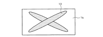
定量バルブ11は、接着剤13が入った容器に接続され、移動ステージ12で移動することで基板1bの表面に所定量の接着剤13を所定のパターン塗布することができる塗布手段である。なお、図1に示す貼り合わせ装置では、定量バルブ11により接着剤13を塗布する構成であるが、本発明ではこれに限られず、例えば接着剤13をスクリーン印刷等で塗布しても良い。
The metering valve 11 is an application means that is connected to a container containing an
次に、図1に示す貼り合わせ装置の概略図を用いて、基板の貼り合わせ方法を示す。なお、背景技術でも説明したように、本明細書においては、液晶パネルや導光体、偏光板等、表示装置を構成する板状のものを基板と総称する。 Next, a method for bonding substrates will be described with reference to the schematic view of the bonding apparatus shown in FIG. Note that, as described in the background art, in the present specification, plate-like objects constituting a display device such as a liquid crystal panel, a light guide, and a polarizing plate are collectively referred to as a substrate.
まず、基板1aを下吸着ベース3上に置き、真空吸着等により下吸着ベース3に基板1aを保持させる。そして、貼り合わせ位置である上吸着ベース2の下まで、移動ガイド5を用いて基板1aを保持する下吸着ベース3を搬送する。その後、基板1aにあるターゲットマーク等の位置情報を画像処理装置9のカメラ8で確認し、補正ガイド4により必要な位置補正を行う。位置補正後、基板1aを真空吸着等により上吸着ベース2に保持させる一方、下吸着ベース3の保持は解除する。これにより、上吸着ベース2は、基板1aを貼り合わせ位置に正確に保持することができる。
First, the substrate 1a is placed on the
次に、基板1bを下吸着ベース3上に置き、真空吸着等により下吸着ベース3に基板1bを保持させる。その後、基板1bの表面に、定量バルブ11と移動ステージ12を使用して所定量の接着剤13を所定のパターンで塗布する。具体的に図1の場合では、移動ガイド5を用いて下吸着ベース3を定量バルブ11の下に移動し、定量バルブ11を用いて所定のパターンの接着剤13を塗布する。なお、本実施の形態では、後述する図3に示すように、所定のパターンとしてX字状を用いる。また、基板1bの表面は、基板1aに相対する側の面である。
Next, the
次に、接着剤13を塗布した基板1bを、移動ガイド5を用いて、貼り合わせ位置である上吸着ベース2の下まで搬送する。搬送後、画像処理装置9のカメラ8を用いて基板1bにあるターゲットマーク等の位置情報を確認し、画像処理装置9から得られた補正情報に基づいて補正ガイド4により、相対する2枚の基板1a、1bの貼り合わせ位置を補正する。
Next, the board |
次に、下吸着ベース3上の基板1bに上吸着ベース2に保持された基板1aを重ね合わせ、加圧ステージ7により所定の加圧力で押し付ける。これにより、相対する2枚の基板1a、1bを貼り合わせることが可能となる。貼り合わされた基板1a、1bに対して、別の基板をさらに貼り合わせる同様の工程を繰り返すことで、複数の基板を貼り合わせることができる。また、接着剤13を塗布する工程と、基板1bの位置補正を行う工程との順序を逆にしても良い。さらに、図1に示すように、全ての機器が架台10上に取り付けされているため、架台10全体をカバー等で覆うことによりゴミの混入や接着剤13の飛散を防止することができる。
Next, the substrate 1 a held on the upper suction base 2 is superposed on the
以上のように、本実施の形態に係る貼り合わせ装置は、上記の構成とすることで、複数の基板1を規定の圧力で加圧し、接着層の厚みを管理することが可能となるので、基板を高精度に貼り合わせることが可能となる。また、本実施の形態に係る貼り合わせ装置では、基板1bの表面にX字状のパターンの接着剤13を塗布するので、基板と2つ以上の接着剤13の液滴間に生じた空間の空気を巻き込むことがなく、接着層に気泡が残存する可能性が低い。
As described above, since the bonding apparatus according to the present embodiment has the above-described configuration, it is possible to pressurize the plurality of
(実施の形態2)
実施の形態1では、上吸着ベース2が加圧ステージ7に直接支持されていたが、本実施の形態では、図2(a)(b)に示すように、球面軸受6を介して上吸着ベース2を加圧ステージ7に支持するような構成に変更している。
(Embodiment 2)
In the first embodiment, the upper suction base 2 is directly supported by the
上吸着ベース2を球面軸受6で加圧ステージ7に支持することにより、上吸着ベース2が球面軸受6を軸に自在に動くことが可能になる。つまり、図2(a)に示すように、上吸着ベース2が下吸着ベース3に対して平行でない場合(上吸着ベース2が右上がりに傾いている)、上吸着ベース2に保持されている基板1aを下吸着ベース3に保持されている基板1bに重ね合わせると、球面軸受6により自動的に基板1a、1b同士の傾きが補正され、平行な接着面を形成することができる(図2(b))。
By supporting the upper suction base 2 on the
以上のように、本実施の形態に係る貼り合わせ装置は、加圧ステージ7が上吸着ベース2を球面軸受6により支持する構成であるので、上吸着ベース2と下吸着ベース3の平行度を精度良く出す必要がなく、押し付け時に均等に加圧することができるので接着層の厚みのばらつきを抑えることができる。
As described above, in the bonding apparatus according to the present embodiment, the
(実施の形態3)
さらに、本実施の形態では、接着剤13の塗布パターン及び貼り合わせ方法について詳細に説明する。まず、図3に、定量バルブ11と移動ステージ12を使用して、下吸着ベース3に保持された基板1bの表面に塗布した接着剤13のパターンを示す。図3に示す接着剤13のパターンは、定量の接着剤13を用いてX字状のパターンとしている。
(Embodiment 3)
Furthermore, in this Embodiment, the application pattern of the
基板1bの表面にX字状のパターンの接着剤13を塗布した後、図4に示すように上吸着ベース2を傾斜させ、基板1aの一つの端辺と、基板1bの一つの端辺とを接触させる。図4では、上吸着ベース2を右上がりに傾け、基板1aの左側の端辺と基板1bの左側の端辺とを接触させている。
After the X-shaped pattern of adhesive 13 is applied to the surface of the
このように、貼り合わせ時に下吸着ベース3に保持した基板1bに対して、上吸着ベース2に保持した基板1bを傾斜させて重ね合わせ、そして、接触した箇所(左側の端辺)を起点に上吸着ベース2を、相対する2枚の基板1a,1bが平行になるまで傾かせながら押し付ける。
In this way, the
このようにして相対する2枚の基板1a,1b貼り合わせることにより、接着剤13は、図5に示すようにX字の頂点から基板1a,1bの四隅に広がりやすくなる。つまり、接着剤13は、左側の端辺近傍から順に潰され広がることになる。なお、図5は、接着剤13が基板1a,1bの左側から中央部まで潰されて広がった時点の接着剤13の塗布パターンを示している。また、背景技術で説明した複数箇所に接着剤13を塗布する場合のように、接着剤13の複数の液滴が接触する際に生じる気泡の巻き込みは、本実施の形態に係る塗布パターンでは生じ難い。
By bonding the two
以上のように、本実施の形態に係る貼り合わせ装置では、加圧手段である加圧ステージ7が、上吸着ベース2上の基板1aに対して、下吸着ベース3に保持された基板1bを傾斜させて重ね合わせ、基板1aが基板1bに接触した箇所を起点に、上吸着ベース2を基板1aと基板1bとが平行になるまで移動させながら加圧するので、基板1a,1bの四隅に接着剤13が広がりやすく、気泡を基板外側に追出すことができるため、接着層に気泡を残存させずに、簡便に接着剤13を基板1a,1b全面に充填することができる。
As described above, in the bonding apparatus according to the present embodiment, the
1a,1b 基板、2 上吸着ベース、3 下吸着ベース、4 補正ガイド、5 移動ガイド、6 球面軸受、7 加圧ステージ、8 カメラ、9 画像処理装置、10 架台、11 定量バルブ、12 移動ステージ、13 接着剤。
1a, 1b Substrate, 2 Upper suction base, 3 Lower suction base, 4 Correction guide, 5 Movement guide, 6 Spherical bearing, 7 Pressure stage, 8 Camera, 9 Image processing device, 10 Mounting base, 11 Metering valve, 12
Claims (3)
第1の基板を保持する第1保持手段と、
前記第1の基板と相対する第2の基板を保持する第2保持手段と、
X字状のパターンとなるように接着剤を、前記第2の基板の表面に塗布する塗布手段と、
前記第1の基板を、前記接着剤が塗布された前記第2の基板に加圧しながら貼り合わせる加圧手段とを備える貼り合わせ装置。 A laminating apparatus for laminating a plurality of substrates,
First holding means for holding a first substrate;
Second holding means for holding a second substrate facing the first substrate;
An application means for applying an adhesive to the surface of the second substrate so as to form an X-shaped pattern;
A laminating apparatus comprising: a pressing unit that bonds the first substrate to the second substrate coated with the adhesive while pressing.
前記加圧手段は、前記第2保持手段上の前記第2の基板に対して、前記第1保持手段に保持された前記第1の基板を傾斜させて重ね合わせ、前記第1の基板が前記第2の基板に接触した箇所を起点に、前記第1保持手段を前記第1の基板と前記第2の基板とが平行になるまで移動させながら加圧することを特徴とする貼り合わせ装置。 The bonding apparatus according to claim 1,
The pressurizing unit tilts and superimposes the first substrate held by the first holding unit on the second substrate on the second holding unit, and the first substrate is A bonding apparatus, wherein pressure is applied while moving the first holding means until the first substrate and the second substrate are parallel, starting from a position in contact with the second substrate.
前記加圧手段は、前記第1保持手段を球面軸受により支持していることを特徴とする貼り合わせ装置。
The bonding apparatus according to claim 2,
The laminating apparatus, wherein the pressurizing means supports the first holding means by a spherical bearing.
Priority Applications (1)
| Application Number | Priority Date | Filing Date | Title |
|---|---|---|---|
| JP2005113245A JP2006292993A (en) | 2005-04-11 | 2005-04-11 | Pasting device |
Applications Claiming Priority (1)
| Application Number | Priority Date | Filing Date | Title |
|---|---|---|---|
| JP2005113245A JP2006292993A (en) | 2005-04-11 | 2005-04-11 | Pasting device |
Publications (1)
| Publication Number | Publication Date |
|---|---|
| JP2006292993A true JP2006292993A (en) | 2006-10-26 |
Family
ID=37413646
Family Applications (1)
| Application Number | Title | Priority Date | Filing Date |
|---|---|---|---|
| JP2005113245A Pending JP2006292993A (en) | 2005-04-11 | 2005-04-11 | Pasting device |
Country Status (1)
| Country | Link |
|---|---|
| JP (1) | JP2006292993A (en) |
Cited By (16)
| Publication number | Priority date | Publication date | Assignee | Title |
|---|---|---|---|---|
| WO2007063751A1 (en) * | 2005-11-29 | 2007-06-07 | Seiko Instruments Inc. | Process for producing display and method of laminating |
| WO2008126893A1 (en) * | 2007-04-10 | 2008-10-23 | Sony Chemical & Information Device Corporation | Method for manufacturing image display device, and image display device |
| JP2010060815A (en) * | 2008-09-03 | 2010-03-18 | Casio Comput Co Ltd | Liquid crystal display panel integrated with protective plate |
| US7910033B2 (en) | 2007-04-03 | 2011-03-22 | Sony Chemical & Information Device Corporation | Method for manufacturing image display device |
| US7927533B2 (en) | 2007-04-04 | 2011-04-19 | Sony Chemical & Information Device Corporation | Method for manufacturing image display device |
| WO2011049197A1 (en) * | 2009-10-23 | 2011-04-28 | 共同技研化学株式会社 | Panel attaching method and panel attaching device |
| JP2011100118A (en) * | 2009-10-07 | 2011-05-19 | Sony Chemical & Information Device Corp | Bonding device and method for manufacturing tabular bonded body |
| CN102109702A (en) * | 2009-12-25 | 2011-06-29 | 东芝移动显示器有限公司 | Manufacturing method of flat-panel display device and adhesive-resin applying apparatus therefor |
| KR101371096B1 (en) | 2012-04-23 | 2014-03-10 | 엘아이지에이디피 주식회사 | Substrate bonding apparatus |
| US8773624B2 (en) | 2007-04-09 | 2014-07-08 | Sony Chemical & Information Device Corporation | Resin composition and image display apparatus |
| US9354462B2 (en) | 2007-04-09 | 2016-05-31 | Dexerials Corporation | Image display device |
| JP2016141131A (en) * | 2015-02-05 | 2016-08-08 | 株式会社リコー | Droplet ejection head, method of manufacturing droplet ejection head and image forming apparatus |
| US9885900B2 (en) | 2006-07-14 | 2018-02-06 | Dexerials Corporation | Resin composition and display unit |
| US9885895B2 (en) | 2007-07-17 | 2018-02-06 | Dexerials Corporation | Image display device and production method thereof |
| CN107830801A (en) * | 2017-10-27 | 2018-03-23 | 东莞东聚电子电讯制品有限公司 | A kind of high-precision sphere laminating apparatus |
| US10216026B2 (en) | 2007-04-09 | 2019-02-26 | Dexerials Corporation | Image display device that can display high brightness and high contrast images and includes a cured resin layer |
Citations (6)
| Publication number | Priority date | Publication date | Assignee | Title |
|---|---|---|---|---|
| JPS6235830U (en) * | 1985-08-23 | 1987-03-03 | ||
| JPH08160407A (en) * | 1994-12-05 | 1996-06-21 | Sharp Corp | Production of liquid crystal display element |
| JPH09211437A (en) * | 1996-02-02 | 1997-08-15 | Matsushita Electric Ind Co Ltd | Liquid crystal display element and its production and apparatus for production therefor |
| JPH112805A (en) * | 1997-06-13 | 1999-01-06 | Sharp Corp | Liquid crystal display device and its manufacture |
| JP2002341359A (en) * | 2001-05-18 | 2002-11-27 | Matsushita Electric Ind Co Ltd | Method and device for manufacturing liquid crystal display element |
| JP2004325788A (en) * | 2003-04-24 | 2004-11-18 | Sony Corp | Method and apparatus for optical inspection, and method for manufacturing liquid crystal display device |
-
2005
- 2005-04-11 JP JP2005113245A patent/JP2006292993A/en active Pending
Patent Citations (6)
| Publication number | Priority date | Publication date | Assignee | Title |
|---|---|---|---|---|
| JPS6235830U (en) * | 1985-08-23 | 1987-03-03 | ||
| JPH08160407A (en) * | 1994-12-05 | 1996-06-21 | Sharp Corp | Production of liquid crystal display element |
| JPH09211437A (en) * | 1996-02-02 | 1997-08-15 | Matsushita Electric Ind Co Ltd | Liquid crystal display element and its production and apparatus for production therefor |
| JPH112805A (en) * | 1997-06-13 | 1999-01-06 | Sharp Corp | Liquid crystal display device and its manufacture |
| JP2002341359A (en) * | 2001-05-18 | 2002-11-27 | Matsushita Electric Ind Co Ltd | Method and device for manufacturing liquid crystal display element |
| JP2004325788A (en) * | 2003-04-24 | 2004-11-18 | Sony Corp | Method and apparatus for optical inspection, and method for manufacturing liquid crystal display device |
Cited By (37)
| Publication number | Priority date | Publication date | Assignee | Title |
|---|---|---|---|---|
| WO2007063751A1 (en) * | 2005-11-29 | 2007-06-07 | Seiko Instruments Inc. | Process for producing display and method of laminating |
| US10684498B2 (en) | 2006-07-14 | 2020-06-16 | Dexerials Corporation | Resin composition and display unit |
| US10989944B2 (en) | 2006-07-14 | 2021-04-27 | Dexerials Corporation | Resin composition and display unit |
| US9885900B2 (en) | 2006-07-14 | 2018-02-06 | Dexerials Corporation | Resin composition and display unit |
| US10989943B2 (en) | 2006-07-14 | 2021-04-27 | Dexerials Corporation | Resin composition and display unit |
| US11467438B2 (en) | 2006-07-14 | 2022-10-11 | Dexerials Corporation | Resin composition and display unit |
| US11982890B2 (en) | 2006-07-14 | 2024-05-14 | Dexerials Corporation | Resin composition and display unit |
| US7910033B2 (en) | 2007-04-03 | 2011-03-22 | Sony Chemical & Information Device Corporation | Method for manufacturing image display device |
| US7927533B2 (en) | 2007-04-04 | 2011-04-19 | Sony Chemical & Information Device Corporation | Method for manufacturing image display device |
| US12147111B2 (en) | 2007-04-09 | 2024-11-19 | Dexerials Corporation | Image display device that can display high brightness and high contrast images and includes a cured resin layer |
| US9354462B2 (en) | 2007-04-09 | 2016-05-31 | Dexerials Corporation | Image display device |
| US11740501B2 (en) | 2007-04-09 | 2023-08-29 | Dexerials Corporation | Image display device that can display high brightness and high contrast images and includes a cured resin layer |
| US10216026B2 (en) | 2007-04-09 | 2019-02-26 | Dexerials Corporation | Image display device that can display high brightness and high contrast images and includes a cured resin layer |
| US8773624B2 (en) | 2007-04-09 | 2014-07-08 | Sony Chemical & Information Device Corporation | Resin composition and image display apparatus |
| US10725329B2 (en) | 2007-04-09 | 2020-07-28 | Dexerials Corporation | Image display device that can display high brightness and high contrast images and includes a cured resin layer |
| US11237423B2 (en) | 2007-04-09 | 2022-02-01 | Dexerials Corporation | Image display device that can display high brightness and high contrast images and includes a cured resin layer |
| JP2009186959A (en) * | 2007-04-10 | 2009-08-20 | Sony Chemical & Information Device Corp | Manufacturing method of image display device |
| JP2015222430A (en) * | 2007-04-10 | 2015-12-10 | デクセリアルズ株式会社 | Manufacturing method of image display device |
| US10876013B2 (en) | 2007-04-10 | 2020-12-29 | Dexerials Corporation | Method for producing image display apparatus |
| JP2017076132A (en) * | 2007-04-10 | 2017-04-20 | デクセリアルズ株式会社 | Method for manufacturing image display device |
| WO2008126893A1 (en) * | 2007-04-10 | 2008-10-23 | Sony Chemical & Information Device Corporation | Method for manufacturing image display device, and image display device |
| JP2014089479A (en) * | 2007-04-10 | 2014-05-15 | Dexerials Corp | Method for manufacturing image display device |
| US11614647B2 (en) | 2007-04-10 | 2023-03-28 | Dexerials Corporation | Method for producing image display apparatus |
| US9885895B2 (en) | 2007-07-17 | 2018-02-06 | Dexerials Corporation | Image display device and production method thereof |
| JP2010060815A (en) * | 2008-09-03 | 2010-03-18 | Casio Comput Co Ltd | Liquid crystal display panel integrated with protective plate |
| KR101752020B1 (en) * | 2009-10-07 | 2017-06-28 | 데쿠세리아루즈 가부시키가이샤 | Bonding device and method for manufacturing tabular bonded body |
| JP2011100118A (en) * | 2009-10-07 | 2011-05-19 | Sony Chemical & Information Device Corp | Bonding device and method for manufacturing tabular bonded body |
| CN102598092A (en) * | 2009-10-23 | 2012-07-18 | 共同技研化学株式会社 | Panel attaching method and panel attaching device |
| KR101698049B1 (en) | 2009-10-23 | 2017-01-19 | 교도 기큰 케미칼 가부시키가이샤 | Panel attaching method and panel attaching device |
| JP5622741B2 (en) * | 2009-10-23 | 2014-11-12 | 共同技研化学株式会社 | Panel sticking method and sticking device |
| KR20120087893A (en) * | 2009-10-23 | 2012-08-07 | 교도 기큰 케미칼 가부시키가이샤 | Panel attaching method and panel attaching device |
| WO2011049197A1 (en) * | 2009-10-23 | 2011-04-28 | 共同技研化学株式会社 | Panel attaching method and panel attaching device |
| CN102109702A (en) * | 2009-12-25 | 2011-06-29 | 东芝移动显示器有限公司 | Manufacturing method of flat-panel display device and adhesive-resin applying apparatus therefor |
| KR101371096B1 (en) | 2012-04-23 | 2014-03-10 | 엘아이지에이디피 주식회사 | Substrate bonding apparatus |
| JP2016141131A (en) * | 2015-02-05 | 2016-08-08 | 株式会社リコー | Droplet ejection head, method of manufacturing droplet ejection head and image forming apparatus |
| CN107830801A (en) * | 2017-10-27 | 2018-03-23 | 东莞东聚电子电讯制品有限公司 | A kind of high-precision sphere laminating apparatus |
| CN107830801B (en) * | 2017-10-27 | 2024-05-28 | 东莞东聚电子电讯制品有限公司 | High-precision spherical surface laminating device |
Similar Documents
| Publication | Publication Date | Title |
|---|---|---|
| JP2006292993A (en) | Pasting device | |
| JP5456656B2 (en) | Method for manufacturing flat display device and adhesive resin coating apparatus therefor | |
| JP5784903B2 (en) | Method for manufacturing plate-like bonded body and apparatus for bonding plate-shaped body | |
| CN101795950A (en) | Vacuum adsorption control mechanism device, film pasting device, method of pasting film, and display device | |
| JP2005093997A5 (en) | ||
| TWI449005B (en) | Functional film lamination method, lamination device and film positioning method | |
| CN101795849B (en) | Vacuum adsorption control mechanism device, film sticking device, display device | |
| KR20130047590A (en) | Sticking apparatus and sticking method | |
| JP2013022760A (en) | Film sticking device | |
| JP5608690B2 (en) | Method for manufacturing flat display device | |
| JP4482395B2 (en) | Substrate bonding method and bonding apparatus | |
| JP5512061B1 (en) | Manufacturing method of bonding device | |
| JP2005156907A (en) | Method and device for manufacturing display device | |
| CN101823356A (en) | Film attaching machine table, film attaching method and manufacturing method of cured film layer | |
| JP2004138973A (en) | Flexographic printing plate, flexographic printing apparatus, method for producing flexographic printing plate, and method for producing printed matter | |
| JP5512259B2 (en) | Method for manufacturing flat display device and attaching device therefor | |
| KR20190070660A (en) | Lamination apparatus and lamination method using the same for reducing the incidence of oca scratches | |
| JP2017045010A (en) | Manufacturing device of member for display and manufacturing method of member for display | |
| JP2009025567A (en) | Optical film affixing method, optical film affixing device, and display panel manufacturing method | |
| JP5389694B2 (en) | Manufacturing method of display device | |
| CN216330697U (en) | Laminating device | |
| KR20160111603A (en) | Breaking system for attached substrate | |
| KR101040248B1 (en) | Liquid crystal panel and its front panel bonding method | |
| KR20140000495A (en) | Laminating device and method for apparatus of bonding substrates, and apparatus and method of bonding substrates having the same | |
| JP2001174835A (en) | Glass substrate assembly device for liquid crystal display device and method for manufacturing liquid crystal display device |
Legal Events
| Date | Code | Title | Description |
|---|---|---|---|
| A621 | Written request for application examination |
Free format text: JAPANESE INTERMEDIATE CODE: A621 Effective date: 20070109 |
|
| RD04 | Notification of resignation of power of attorney |
Free format text: JAPANESE INTERMEDIATE CODE: A7424 Effective date: 20091106 |
|
| A977 | Report on retrieval |
Free format text: JAPANESE INTERMEDIATE CODE: A971007 Effective date: 20091228 |
|
| A131 | Notification of reasons for refusal |
Free format text: JAPANESE INTERMEDIATE CODE: A131 Effective date: 20100202 |
|
| A02 | Decision of refusal |
Free format text: JAPANESE INTERMEDIATE CODE: A02 Effective date: 20100608 |