JP2006143497A - Apparatus for manufacturing silicon carbide single crystal - Google Patents
Apparatus for manufacturing silicon carbide single crystal Download PDFInfo
- Publication number
- JP2006143497A JP2006143497A JP2004333222A JP2004333222A JP2006143497A JP 2006143497 A JP2006143497 A JP 2006143497A JP 2004333222 A JP2004333222 A JP 2004333222A JP 2004333222 A JP2004333222 A JP 2004333222A JP 2006143497 A JP2006143497 A JP 2006143497A
- Authority
- JP
- Japan
- Prior art keywords
- silicon carbide
- single crystal
- carbide single
- raw material
- heat insulating
- Prior art date
- Legal status (The legal status is an assumption and is not a legal conclusion. Google has not performed a legal analysis and makes no representation as to the accuracy of the status listed.)
- Pending
Links
- 239000013078 crystal Substances 0.000 title claims abstract description 102
- HBMJWWWQQXIZIP-UHFFFAOYSA-N silicon carbide Chemical compound [Si+]#[C-] HBMJWWWQQXIZIP-UHFFFAOYSA-N 0.000 title claims abstract description 84
- 229910010271 silicon carbide Inorganic materials 0.000 title claims abstract description 83
- 238000004519 manufacturing process Methods 0.000 title claims abstract description 58
- 239000002994 raw material Substances 0.000 claims abstract description 52
- 238000000859 sublimation Methods 0.000 claims abstract description 50
- 230000008022 sublimation Effects 0.000 claims abstract description 50
- OKTJSMMVPCPJKN-UHFFFAOYSA-N Carbon Chemical compound [C] OKTJSMMVPCPJKN-UHFFFAOYSA-N 0.000 claims description 9
- 229910002804 graphite Inorganic materials 0.000 claims description 8
- 239000010439 graphite Substances 0.000 claims description 8
- 239000000843 powder Substances 0.000 claims description 8
- 238000005092 sublimation method Methods 0.000 claims description 6
- XUIMIQQOPSSXEZ-UHFFFAOYSA-N Silicon Chemical compound [Si] XUIMIQQOPSSXEZ-UHFFFAOYSA-N 0.000 claims description 2
- 229910052710 silicon Inorganic materials 0.000 claims description 2
- 239000010703 silicon Substances 0.000 claims description 2
- 238000003860 storage Methods 0.000 claims description 2
- 238000003763 carbonization Methods 0.000 claims 1
- 238000009826 distribution Methods 0.000 abstract description 8
- 238000009413 insulation Methods 0.000 description 15
- 238000000034 method Methods 0.000 description 10
- 238000012986 modification Methods 0.000 description 9
- 230000004048 modification Effects 0.000 description 9
- 230000000694 effects Effects 0.000 description 8
- 239000000463 material Substances 0.000 description 7
- 238000009529 body temperature measurement Methods 0.000 description 5
- 238000010438 heat treatment Methods 0.000 description 5
- 239000011810 insulating material Substances 0.000 description 4
- 238000002791 soaking Methods 0.000 description 4
- 230000000052 comparative effect Effects 0.000 description 3
- 230000007547 defect Effects 0.000 description 3
- 230000005484 gravity Effects 0.000 description 3
- 238000005304 joining Methods 0.000 description 3
- BOTDANWDWHJENH-UHFFFAOYSA-N Tetraethyl orthosilicate Chemical compound CCO[Si](OCC)(OCC)OCC BOTDANWDWHJENH-UHFFFAOYSA-N 0.000 description 1
- 230000002411 adverse Effects 0.000 description 1
- 239000003513 alkali Substances 0.000 description 1
- 239000012300 argon atmosphere Substances 0.000 description 1
- 239000012298 atmosphere Substances 0.000 description 1
- 230000015572 biosynthetic process Effects 0.000 description 1
- 229910052799 carbon Inorganic materials 0.000 description 1
- 230000015556 catabolic process Effects 0.000 description 1
- 238000010586 diagram Methods 0.000 description 1
- 238000005530 etching Methods 0.000 description 1
- 238000002474 experimental method Methods 0.000 description 1
- 239000012535 impurity Substances 0.000 description 1
- 230000006698 induction Effects 0.000 description 1
- 239000002184 metal Substances 0.000 description 1
- 238000002156 mixing Methods 0.000 description 1
- 239000000203 mixture Substances 0.000 description 1
- 230000003287 optical effect Effects 0.000 description 1
- 239000002245 particle Substances 0.000 description 1
- 239000005011 phenolic resin Substances 0.000 description 1
- 229920000642 polymer Polymers 0.000 description 1
- 230000005855 radiation Effects 0.000 description 1
- 238000011160 research Methods 0.000 description 1
- 229920003987 resole Polymers 0.000 description 1
- 239000004065 semiconductor Substances 0.000 description 1
- 239000000758 substrate Substances 0.000 description 1
- 239000011800 void material Substances 0.000 description 1
- 235000012431 wafers Nutrition 0.000 description 1
Images


Landscapes
- Crystals, And After-Treatments Of Crystals (AREA)
Abstract
Description
本発明は炭化ケイ素単結晶製造装置に関する。 The present invention relates to an apparatus for producing a silicon carbide single crystal.
炭化ケイ素単結晶は、パワーデバイス等の半導体装置製造用基板材料として注目されており、現在の技術動向からさらなる高品質化と大型化が求められている。この炭化ケイ素単結晶の製造方法の1つとして、昇華法により炭化ケイ素単結晶を成長させる方法(改良レイリー法)がある。改良レイリー法において、結晶を大型化し、また生産性を向上させるためには、原料粉内の温度分布がなるべく一様になるようにして原料粉を効率的に昇華させることが求められる。 Silicon carbide single crystal is attracting attention as a substrate material for manufacturing semiconductor devices such as power devices, and further higher quality and larger size are demanded from current technological trends. One method for producing this silicon carbide single crystal is a method (an improved Rayleigh method) for growing a silicon carbide single crystal by a sublimation method. In the improved Rayleigh method, in order to increase the crystal size and improve the productivity, it is required to efficiently sublimate the raw material powder so that the temperature distribution in the raw material powder is as uniform as possible.
ここで、図11に示すように従来の炭化ケイ素単結晶製造装置110は、昇華用原料104を収容可能とする容器(坩堝)111と、容器111に着脱自在に取り付けられると共に種結晶105を配置可能とする蓋112と、を有する。また、容器111の内部を高温に保つため、炭化ケイ素単結晶製造装置110の外周は断熱材109で覆われている。さらに、結晶成長時の昇華用原料104の温度を観察するため、容器111の下方(重力方向)に、断熱材109に穴を設けて形成された温度計測用窓108が配置されている。そして、容器111に昇華用原料104を詰め、これを外部に設けた加熱手段(図示せず)で加熱し、昇華した炭化ケイ素を種結晶105上に再結晶させることで炭化ケイ素単結晶が製造される。
Here, as shown in FIG. 11, a conventional silicon carbide single
ところが、従来の炭化ケイ素単結晶製造装置110の構成では温度計測用窓108から熱が逃げるため、昇華用原料104の、温度計測用窓108に近く位置する領域では昇華用原料104の温度上昇が妨げられ、昇華せずに残留したり固化する傾向があった。また、昇華用原料104内の温度分布が均一でないため、昇華速度も一様でなく、ひいてはこれが結晶の質にも悪影響を与える傾向があった。
However, in the configuration of the conventional silicon carbide single
前述の問題を解決する手段としていくつかの技術が提案されている(例えば、特許文献1参照。)が、容器(坩堝)の外周を断熱材で覆うだけでは、温度計測用窓108からの熱の放出を効果的に防止することは困難であった。
以上より、炭化ケイ素単結晶製造装置の昇華用原料配置部の温度分布を均一に保てる装置が求められていた。即ち、炭化ケイ素単結晶が効率良く成長し、最終的に大型で高純度の炭化ケイ素単結晶が得られる炭化ケイ素単結晶製造装置が求められていた。 In view of the above, there has been a demand for an apparatus capable of maintaining a uniform temperature distribution in the sublimation raw material placement portion of the silicon carbide single crystal production apparatus. That is, there has been a demand for a silicon carbide single crystal production apparatus capable of efficiently growing a silicon carbide single crystal and finally obtaining a large and high-purity silicon carbide single crystal.
本発明は以下の記載事項に関する:
(1) 昇華させた炭化ケイ素を種結晶上に再結晶させて炭化ケイ素単結晶を製造するための、昇華用原料を収容する容器と、昇華用原料に対向して設けられた種結晶配置部とを備える炭化ケイ素単結晶製造装置であって、上記昇華用原料を収容する容器は、昇華用原料収容部の底部に断熱層を具備する断熱部を備える炭化ケイ素単結晶製造装置。
The present invention relates to the following items:
(1) A container for containing a sublimation raw material for producing a silicon carbide single crystal by recrystallizing sublimated silicon carbide on a seed crystal, and a seed crystal arrangement portion provided facing the sublimation raw material A silicon carbide single crystal manufacturing apparatus comprising: a container for storing the sublimation raw material, comprising a heat insulating portion including a heat insulating layer at a bottom of the sublimation raw material storage portion.
(2) 前記断熱部に前記断熱層として、上記昇華用原料を収容する容器よりも熱伝導率の低い部材が設けられている上記(1)記載の炭化ケイ素単結晶製造装置。 (2) The silicon carbide single crystal manufacturing apparatus according to (1), wherein a member having a lower thermal conductivity than that of the container that houses the sublimation raw material is provided as the heat insulating layer in the heat insulating portion.
(3) 上記昇華用原料を収容する容器よりも熱伝導率の低い部材は、昇華法における高温時の黒鉛の熱伝導率の50%以下である上記(2)記載の炭化ケイ素単結晶製造装置。 (3) The silicon carbide single crystal manufacturing apparatus according to (2), wherein the member having a lower thermal conductivity than the container for storing the sublimation raw material is 50% or less of the thermal conductivity of graphite at a high temperature in the sublimation method. .
(4) 前記断熱部に前記断熱層として、空隙が設けられている上記(1)記載の炭化ケイ素単結晶製造装置。 (4) The silicon carbide single crystal manufacturing apparatus according to (1), wherein a gap is provided as the heat insulating layer in the heat insulating portion.
(5) 上記炭化ケイ素単結晶製造装置の縦方向の高さをLとし、断熱部の厚みの最大値をTとしたときに、T/Lが0.01以上である上記(1)〜(4)のいずれかに記載の炭化ケイ素単結晶製造装置。 (5) When the height in the vertical direction of the silicon carbide single crystal manufacturing apparatus is L and the maximum thickness of the heat insulating portion is T, T / L is 0.01 or more. 4) The silicon carbide single crystal production apparatus according to any one of 4).
(6) 前記昇華用原料粉の投影面積をS1とし、前記断熱層の投影面積をS2としたときに、S2/S1が0.2以上1.1以下である上記(1)記載の炭化ケイ素単結晶製造装置。 (6) The silicon carbide according to (1), wherein S2 / S1 is 0.2 or more and 1.1 or less when the projected area of the sublimation raw material powder is S1 and the projected area of the heat insulating layer is S2. Single crystal manufacturing equipment.
本発明によれば、昇華用原料配置部の温度分布を均一に保てる炭化ケイ素単結晶製造装置が提供される。即ち、本発明によれば、炭化ケイ素単結晶が効率良く成長し、最終的に大型で高純度の炭化ケイ素単結晶が得られる炭化ケイ素単結晶製造装置が提供される。 ADVANTAGE OF THE INVENTION According to this invention, the silicon carbide single crystal manufacturing apparatus which can maintain the temperature distribution of the sublimation raw material arrangement | positioning part uniform is provided. That is, according to the present invention, there is provided a silicon carbide single crystal production apparatus capable of efficiently growing a silicon carbide single crystal and finally obtaining a large and high-purity silicon carbide single crystal.
本発明者らは鋭意研究した結果、昇華用原料を収容する容器底部の、昇華用原料粉と温度観察窓の間に、熱伝導率の低い部材や空隙部からなる断熱層を備える断熱部を設けることにより、昇華用原料粉から観測窓への熱の流れが抑制できることを見出した。以下、本発明の実施形態について図面を参照しながら説明する。尚、本発明は以下の実施形態に限定されないことはいうまでもない。また同様の機能を有するものについては同様の符号を付すことで説明を省略する。 As a result of diligent research, the inventors of the present invention have provided a heat insulating portion provided with a heat insulating layer made of a member having a low thermal conductivity or a gap between the sublimation raw material powder and the temperature observation window at the bottom of the container that contains the sublimation raw material. It has been found that the heat flow from the sublimation raw material powder to the observation window can be suppressed by providing. Hereinafter, embodiments of the present invention will be described with reference to the drawings. Needless to say, the present invention is not limited to the following embodiments. Moreover, what has the same function attaches | subjects the same code | symbol, and abbreviate | omits description.
図1に示すように、本発明の実施形態にかかる炭化ケイ素単結晶製造装置10は、昇華用原料4を収容可能とする容器11と、容器11に着脱自在に取り付けられると共に種結晶5を配置可能とする蓋12と、を有する。さらに、炭化ケイ素単結晶製造装置10の外周には、断熱材9a、9b、9cが配置されており、容器11の下方(重力方向)に、容器11の温度計測用窓8が設けられている。また容器11の底部の昇華用原料4と温度観察窓8の間に、断熱部6が設けられている。
As shown in FIG. 1, a silicon carbide single
ここで、容器11としては、容器11内部に炭化ケイ素の昇華雰囲気を形成できるものであれば特に制限はない。容器11としては例えば坩堝を用いることができるが、その材質は黒鉛であることが好ましく、熱膨張係数が種結晶と略同一であるものがさらに好ましい。昇華用原料4を収納しやすくする観点から、容器11と、蓋12は着脱自在に一体に形成されていることが好ましい。接合手段としては、容器11内部の密閉性が保たれるのであればいずれの接合手段を用いても構わない。接合手段としては、例えば図1に示されるような螺合手段が挙げられる。
Here, the
また蓋12としては、炭化ケイ素単結晶の種結晶5を設置可能とするものであって、その材質が黒鉛であるものが好ましく、熱膨張係数が種結晶と略同一であるものがさらに好ましい。
Moreover, as the lid |
断熱部6としては、温度観察用窓からの熱の放出を制御できるものであれば特に制限はないが、断熱層6aと断熱部形成部材6bとを備えることが好ましい。断熱層6aは例えば空隙部又は容器11よりも熱伝導率の低い部材を断熱部6に配置することにより形成される。断熱部形成部材6bとしては容器11と同一の部材とすることができる。容器11よりも熱伝導率の低い部材としては、昇華法における高温時の黒鉛の熱伝導率の50%以下、より好ましくは20%以下の部材を配置することが都合がよい。かかる熱伝導率の下限値は特に制限されるものではないが、昇華法における高温時の黒鉛の熱伝導率の10%程度である。尚、黒鉛の熱伝導率は、20〜40W/mkである。
The heat insulating part 6 is not particularly limited as long as it can control the release of heat from the temperature observation window, but preferably includes a
図2(a)に示すように、炭化ケイ素単結晶製造装置10の縦方向(重力方向)の高さをLとし、断熱層6aの厚みの最大値をTとしたときに、T/Lが0.01以上、より好ましくは、8%以上であることが都合がよい。
As shown in FIG. 2A, when the height in the longitudinal direction (gravity direction) of the silicon carbide single
また、図2(b)に示すように、昇華用原料4の投影面積、即ち容器11の内法面積をS1とし、断熱層6aの投影面積をS2としたときに、S2/S1が20%以上110%以下であることが好ましい。
Further, as shown in FIG. 2B, when the projected area of the sublimation
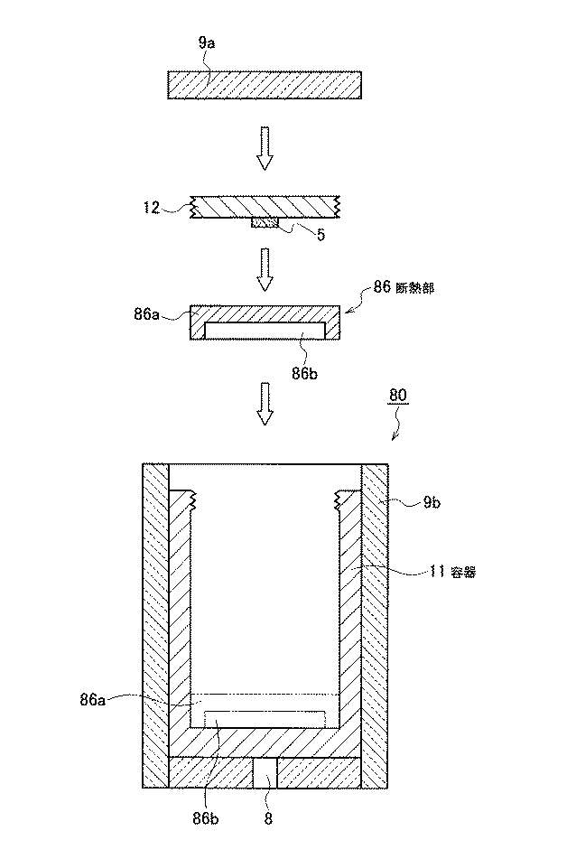
断熱部6の取付け方法としては均熱効果が得られるのであれば特に制限はないが、例えば図3に示すように容器11の底部に設けられた、内壁にねじ山を備える中空部に断熱部6をねじ込み式に取付ける方法が挙げられる。
A method for attaching the heat insulating portion 6 is not particularly limited as long as a soaking effect can be obtained. For example, as shown in FIG. 3, the heat insulating portion is provided in a hollow portion provided at the bottom of the
次に、第1の実施形態の作用効果について、従来の炭化ケイ素単結晶製造装置と比較しつつ説明する。図12は従来型(空隙のない)の炭化ケイ素単結晶製造装置110における熱の流れを示した図である。通常の昇華法においては容器111(坩堝)は誘導加熱により主にその側壁部が熱せられる。その熱は容器111の側壁、底部を伝わって一部は昇華用原料104に伝わるが、残りの大部分は温測窓108から幅射として外へ逃げてしまう。
Next, the operational effects of the first embodiment will be described in comparison with a conventional silicon carbide single crystal manufacturing apparatus. FIG. 12 is a diagram showing the heat flow in the conventional (without voids) silicon carbide single
ところが、図4のように、第1の実施形態によれば、容器11の底に伝わる熱の大部分が昇華用原料4へ伝わるので、昇華用原料4をより均一に熱することが可能になる。つまり、昇華用原料4が効果的に昇華するため、炭化ケイ素単結晶6が効率良く成長し、最終的に大型で高純度の炭化ケイ素単結晶が得られる。
However, as shown in FIG. 4, according to the first embodiment, most of the heat transferred to the bottom of the
(実施形態の変形例)
次に、実施形態の変形例について説明する:
上記実施形態においては、断熱部6はねじ込み式に容器11に取り付けられる構成とした。しかし、断熱部6の取り付け方法はねじ込み式に限定されない。例えば、図5及び図6に示すように、蓋部12を取り外し、容器11の開口部を介して容器11の底部に断熱部6を配置してもよい。
(Modification of the embodiment)
Next, a modification of the embodiment will be described:
In the said embodiment, the heat insulation part 6 was set as the structure attached to the
また実施形態で説明した断熱部の断面形状は、特に制限されるものではない。そのため、断熱部の断面形状を図7〜10に示す形状とすることができる。 Moreover, the cross-sectional shape of the heat insulation part demonstrated by embodiment is not restrict | limited in particular. Therefore, the cross-sectional shape of the heat insulating portion can be the shape shown in FIGS.
即ち、図7に示すように、Dの字を90度時計方向に回転させた断面形状である断熱層26aを備える断熱部26を配置することができる。このような構成とすることで凹レンズ効果により輻射熱が坩堝底部中央に集中するという作用効果が得られる。また、図8に示すように、原料紛内の等温線に沿ってそれぞれ設けられた突起状の断熱部形成部材36bと断熱層36aとを備える断熱部36を配置し、原料紛内の温度分布の均熱化を図ることもできる。図9に示すように、断熱部形成部材46bの厚みが容器11の中心部で厚くなるように形成された断熱部46を配置することで均熱効果の増大を図ることもできる。図10に示すように、容器11の中心部で厚くなるようにステップ状に形成された断熱層56aを備える断熱部56を配置することで均熱効果の増大を図ることもできる。
That is, as shown in FIG. 7, the heat insulation part 26 provided with the
(炭化ケイ素単結晶の製造方法)
以上本発明の炭化ケイ素単結晶製造装置の実施形態について説明してきたが、本発明の別形態として炭化ケイ素単結晶の製造方法が提供される。
即ち、本発明の別の形態として、昇華用原料を収容する容器に昇華用原料を収容し、昇華用原料に略対向して種結晶を配置し、昇華させた昇華用原料を種結晶上に再結晶させて炭化ケイ素単結晶を成長させる炭化ケイ素単結晶の製造方法であって、昇華用原料を昇華させるに際し、昇華用原料を収容する容器の底部に前述の容器と一体に形成された、断熱層を具備する断熱部を配置させる炭化ケイ素単結晶の製造方法が提供される。
(Method for producing silicon carbide single crystal)
As mentioned above, although the embodiment of the silicon carbide single crystal manufacturing apparatus of this invention was described, the manufacturing method of a silicon carbide single crystal is provided as another form of this invention.
That is, as another embodiment of the present invention, the sublimation raw material is housed in a container containing the sublimation raw material, the seed crystal is disposed substantially opposite to the sublimation raw material, and the sublimated raw material is sublimated on the seed crystal. A method for producing a silicon carbide single crystal that is recrystallized to grow a silicon carbide single crystal, which is formed integrally with the aforementioned container at the bottom of a container that contains the sublimation raw material when sublimating the sublimation raw material. There is provided a method for producing a silicon carbide single crystal in which a heat insulating portion having a heat insulating layer is disposed.
この製造方法を実施する場合、実施形態及びその変形例を挙げて説明した前述の炭化ケイ素単結晶製造装置を用いることが好ましい。 When implementing this manufacturing method, it is preferable to use the above-mentioned silicon carbide single crystal manufacturing apparatus described with reference to the embodiment and its modifications.
昇華用原料としては従来公知の材料を用いることができる。昇華用原料としては、例えば高純度のテトラエトキシシラン重合体をケイ素源とし、レゾール型フェノール樹脂を炭素源とし、これらを均一に混合して得た混合物をアルゴン雰囲気下で加熱焼成して得られた炭化ケイ素粉末を用いることができる。また炭化ケイ素単結晶の種結晶としては、従来公知の単結晶を用いることができる。
昇華用原料の加熱温度等の加熱条件は、特に制限されることなく周知の技術に基づいて当業者により適宜設定されうる。
A conventionally known material can be used as a raw material for sublimation. As a sublimation raw material, for example, a high purity tetraethoxysilane polymer is used as a silicon source, a resol type phenol resin is used as a carbon source, and a mixture obtained by uniformly mixing these is heated and fired in an argon atmosphere. Silicon carbide powder can be used. A conventionally known single crystal can be used as the seed crystal of the silicon carbide single crystal.
The heating conditions such as the heating temperature of the sublimation raw material are not particularly limited, and can be appropriately set by those skilled in the art based on known techniques.
(炭化ケイ素単結晶)
本発明の炭化ケイ素単結晶は、前述の炭化ケイ素単結晶の製造方法により製造される:
本発明の炭化ケイ素単結晶は、溶融アルカリによりエッチングして評価した結晶欠陥(パイプ欠陥)が100個/cm2以下であるのが好ましく、50個/cm2以下であるのがより好ましく、10個/cm2以下であるのが特に好ましい。
炭化ケイ素単結晶における金属不純物元素の総含有量としては、10ppm以下が好ましい。
(Silicon carbide single crystal)
The silicon carbide single crystal of the present invention is produced by the aforementioned method for producing a silicon carbide single crystal:
In the silicon carbide single crystal of the present invention, crystal defects (pipe defects) evaluated by etching with molten alkali are preferably 100 pieces / cm 2 or less, more preferably 50 pieces / cm 2 or less. It is particularly preferable that the number of particles / cm 2 or less.
The total content of metal impurity elements in the silicon carbide single crystal is preferably 10 ppm or less.
本発明により得られる炭化ケイ素単結晶は、多結晶や多型の混入やマイクロパイプ等の結晶欠陥がなく、極めて高品質であるので、絶縁破壊特性、耐熱性、耐放射線性等に優れ、半導体ウエハ等の電子デバイス、発光ダイオード等の光学デバイスなどに特に好適に用いられる。 The silicon carbide single crystal obtained by the present invention is free from crystal defects such as polycrystals, polymorphs, and micropipes, and is extremely high quality. Therefore, the silicon carbide single crystal is excellent in dielectric breakdown characteristics, heat resistance, radiation resistance, etc. It is particularly suitably used for electronic devices such as wafers and optical devices such as light emitting diodes.
以上、本発明の炭化ケイ素単結晶製造装置によると、高品質な炭化ケイ素単結晶を効率よく、かつ割れ等の破損がない状態で容易に製造することができる。 As described above, according to the silicon carbide single crystal production apparatus of the present invention, a high-quality silicon carbide single crystal can be produced easily and efficiently without being damaged such as cracks.
(実施例1〜6)
まず、表1に示す条件の断熱部が備えられた図1の炭化ケイ素単結晶製造装置(実施例1〜6)を用意した。次に、図1の装置を、装置外部(図示せず)に設けた加熱手段を設けて加熱した。そして、容器底部の中央部(図中A点)と、容器底部の側壁近傍(図中B点)の温度を測定した。得られた測定値からA点からの距離をX軸とし、A点とB点の温度差をY軸として図13にプロットした。
(Examples 1-6)
First, the silicon carbide single crystal manufacturing apparatus (Examples 1-6) of FIG. 1 provided with the heat insulation part of the conditions shown in Table 1 was prepared. Next, the apparatus of FIG. 1 was heated by providing heating means provided outside the apparatus (not shown). And the temperature of the center part (A point in a figure) of a container bottom part and the side wall vicinity (B point in a figure) of a container bottom part was measured. From the obtained measured values, the distance from point A was plotted on the X axis, and the temperature difference between points A and B was plotted on the Y axis in FIG.
(比較例1)
図11の断熱部が備えられていない従来型の炭化ケイ素単結晶製造装置(比較例1)を用いたことを除いて、実施例1〜6と同様に実験を行った。得られた実験結果をまとめて表1に示す。
Experiments were performed in the same manner as in Examples 1 to 6 except that a conventional silicon carbide single crystal manufacturing apparatus (Comparative Example 1) without the heat insulating portion of FIG. 11 was used. The obtained experimental results are summarized in Table 1.
実施例では比較例と比べて、中央(A点)での温度が高く、底部温度を均一化する効果がある。そして断熱層の熱伝導率が坩堝材の20%である場合と、断熱層として空隙を配置した場合は、温度分布はほぼ同様な効果がある。ただし、断熱層の熱伝導率が坩堝材(黒鉛)の50%以下になる場合、断熱層(空隙)の厚みが小さくなる場合(坩堝厚み対比1%以下)、面積が小さくなる場合(坩堝内面積の20%以下)に、均熱効果が減少する。 In the embodiment, the temperature at the center (point A) is higher than that of the comparative example, and the bottom temperature is made uniform. And when the heat conductivity of a heat insulation layer is 20% of a crucible material, and when a space | gap is arrange | positioned as a heat insulation layer, a temperature distribution has a substantially the same effect. However, when the thermal conductivity of the heat insulating layer is 50% or less of the crucible material (graphite), when the thickness of the heat insulating layer (void) is small (1% or less compared to the crucible thickness), when the area is small (inside the crucible) The soaking effect is reduced to 20% or less of the area).
(b)本発明の実施形態にかかる炭化ケイ素単結晶製造装置10のA1−A1概略断面図を示す。
4、104…昇華用原料
5、105…種結晶
6、26、36,46,56、86、106…断熱部
6a、26a、36a、46a、56a、86a…断熱層
6b、26b、36b、46b、56b、86b…断熱部形成部材
8、108…温度観察用窓
9、109…断熱材
10、110…炭化ケイ素単結晶
10、20、30、40、50,60,80,110…炭化ケイ素単結晶製造装置
11、111…容器
12、112…蓋(種結晶配置部)
4, 104 ... Raw materials for
Claims (6)
前記昇華用原料を収容する容器は、昇華用原料収容部の底部に断熱層を具備する断熱部を備えることを特徴とする炭化ケイ素単結晶製造装置。 A container for containing a sublimation raw material for producing a silicon carbide single crystal by recrystallizing sublimated silicon carbide on a seed crystal, and a seed crystal arrangement portion provided facing the sublimation raw material A silicon carbide single crystal manufacturing apparatus,
The container for storing the sublimation raw material includes a heat insulating portion including a heat insulating layer at the bottom of the sublimation raw material storage portion.
Priority Applications (1)
| Application Number | Priority Date | Filing Date | Title |
|---|---|---|---|
| JP2004333222A JP2006143497A (en) | 2004-11-17 | 2004-11-17 | Apparatus for manufacturing silicon carbide single crystal |
Applications Claiming Priority (1)
| Application Number | Priority Date | Filing Date | Title |
|---|---|---|---|
| JP2004333222A JP2006143497A (en) | 2004-11-17 | 2004-11-17 | Apparatus for manufacturing silicon carbide single crystal |
Publications (1)
| Publication Number | Publication Date |
|---|---|
| JP2006143497A true JP2006143497A (en) | 2006-06-08 |
Family
ID=36623614
Family Applications (1)
| Application Number | Title | Priority Date | Filing Date |
|---|---|---|---|
| JP2004333222A Pending JP2006143497A (en) | 2004-11-17 | 2004-11-17 | Apparatus for manufacturing silicon carbide single crystal |
Country Status (1)
| Country | Link |
|---|---|
| JP (1) | JP2006143497A (en) |
Cited By (8)
| Publication number | Priority date | Publication date | Assignee | Title |
|---|---|---|---|---|
| CN102732953A (en) * | 2011-04-12 | 2012-10-17 | 李汶军 | Technology and apparatus for growing single silicon carbide crystals through double seed crystal-assisted vapor transport method |
| JP2012206876A (en) * | 2011-03-29 | 2012-10-25 | Shin Etsu Handotai Co Ltd | APPARATUS FOR GROWING SiC |
| JP2013212952A (en) * | 2012-04-02 | 2013-10-17 | Sumitomo Electric Ind Ltd | Method for manufacturing silicon carbide single crystal |
| JP2016034880A (en) * | 2014-08-01 | 2016-03-17 | 住友電気工業株式会社 | Production method of monocrystal |
| JP2020083704A (en) * | 2018-11-26 | 2020-06-04 | 昭和電工株式会社 | Method for manufacturing SiC single crystal ingot |
| CN111235630A (en) * | 2020-03-26 | 2020-06-05 | 哈尔滨科友半导体产业装备与技术研究院有限公司 | PVT method double-seed crystal single crystal preparation method and thermal field |
| JP2020093965A (en) * | 2018-12-14 | 2020-06-18 | 昭和電工株式会社 | APPARATUS FOR MANUFACTURING SiC SINGLE CRYSTAL, AND SiC SINGLE CRYSTAL MANUFACTURING STRUCTURE |
| WO2025049130A1 (en) * | 2023-08-25 | 2025-03-06 | Cvd Equipment Corporation | Pvt system with improved crucible design |
Citations (3)
| Publication number | Priority date | Publication date | Assignee | Title |
|---|---|---|---|---|
| JPH0230699A (en) * | 1988-04-13 | 1990-02-01 | Nippon Steel Corp | Growing method of silicon carbide single crystal and device therefor |
| JPH03153594A (en) * | 1989-11-10 | 1991-07-01 | Toshiba Corp | Device for producing semiconductor single crystal |
| JP2002520252A (en) * | 1998-07-14 | 2002-07-09 | シーメンス アクチエンゲゼルシヤフト | Method for producing SiC single crystal |
-
2004
- 2004-11-17 JP JP2004333222A patent/JP2006143497A/en active Pending
Patent Citations (3)
| Publication number | Priority date | Publication date | Assignee | Title |
|---|---|---|---|---|
| JPH0230699A (en) * | 1988-04-13 | 1990-02-01 | Nippon Steel Corp | Growing method of silicon carbide single crystal and device therefor |
| JPH03153594A (en) * | 1989-11-10 | 1991-07-01 | Toshiba Corp | Device for producing semiconductor single crystal |
| JP2002520252A (en) * | 1998-07-14 | 2002-07-09 | シーメンス アクチエンゲゼルシヤフト | Method for producing SiC single crystal |
Cited By (15)
| Publication number | Priority date | Publication date | Assignee | Title |
|---|---|---|---|---|
| JP2012206876A (en) * | 2011-03-29 | 2012-10-25 | Shin Etsu Handotai Co Ltd | APPARATUS FOR GROWING SiC |
| CN102732953A (en) * | 2011-04-12 | 2012-10-17 | 李汶军 | Technology and apparatus for growing single silicon carbide crystals through double seed crystal-assisted vapor transport method |
| JP2013212952A (en) * | 2012-04-02 | 2013-10-17 | Sumitomo Electric Ind Ltd | Method for manufacturing silicon carbide single crystal |
| JP2016034880A (en) * | 2014-08-01 | 2016-03-17 | 住友電気工業株式会社 | Production method of monocrystal |
| US9777400B2 (en) | 2014-08-01 | 2017-10-03 | Sumitomo Electric Industries, Ltd. | Method for producing single crystal |
| JP2020083704A (en) * | 2018-11-26 | 2020-06-04 | 昭和電工株式会社 | Method for manufacturing SiC single crystal ingot |
| US11761114B2 (en) | 2018-11-26 | 2023-09-19 | Resonac Corporation | Method of producing SiC single crystal ingot |
| JP7242978B2 (en) | 2018-11-26 | 2023-03-22 | 株式会社レゾナック | Manufacturing method of SiC single crystal ingot |
| CN111321468B (en) * | 2018-12-14 | 2022-04-26 | 昭和电工株式会社 | Apparatus for producing SiC single crystal and structure for producing SiC single crystal |
| CN111321468A (en) * | 2018-12-14 | 2020-06-23 | 昭和电工株式会社 | SiC single crystal production apparatus and structure for SiC single crystal production |
| US11427927B2 (en) | 2018-12-14 | 2022-08-30 | Showa Denko K.K. | SiC single crystal manufacturing apparatus and structure having container and filler for manufacturing SiC single crystal |
| JP7217627B2 (en) | 2018-12-14 | 2023-02-03 | 昭和電工株式会社 | SiC single crystal manufacturing apparatus and structure for manufacturing SiC single crystal |
| JP2020093965A (en) * | 2018-12-14 | 2020-06-18 | 昭和電工株式会社 | APPARATUS FOR MANUFACTURING SiC SINGLE CRYSTAL, AND SiC SINGLE CRYSTAL MANUFACTURING STRUCTURE |
| CN111235630A (en) * | 2020-03-26 | 2020-06-05 | 哈尔滨科友半导体产业装备与技术研究院有限公司 | PVT method double-seed crystal single crystal preparation method and thermal field |
| WO2025049130A1 (en) * | 2023-08-25 | 2025-03-06 | Cvd Equipment Corporation | Pvt system with improved crucible design |
Similar Documents
| Publication | Publication Date | Title |
|---|---|---|
| US11761117B2 (en) | SiC single crystal sublimation growth apparatus | |
| JP4514339B2 (en) | Method and apparatus for growing silicon carbide single crystal | |
| JP4736401B2 (en) | Method for producing silicon carbide single crystal | |
| JP5304600B2 (en) | SiC single crystal manufacturing apparatus and manufacturing method | |
| JP2011168447A (en) | METHOD FOR PRODUCING SiC SINGLE CRYSTAL | |
| CN103282558A (en) | Device for producing sic single crystals, jig used in said production device, and method of producing sic single crystals | |
| KR101336748B1 (en) | Polycrystalline ingot growth equipment | |
| JP2021102533A (en) | MANUFACTURING METHOD OF SiC SINGLE CRYSTAL | |
| JP2012184120A (en) | APPARATUS FOR MANUFACTURING SiC SINGLE CRYSTAL | |
| JP2011178590A (en) | Component-adjustment member and single crystal growth device provided therewith | |
| KR101299037B1 (en) | Apparatus for growing single crystal using micro-wave and method for growing the same | |
| JP2020040844A (en) | MANUFACTURING METHOD OF SiC SINGLE CRYSTAL, AND COATED MEMBER | |
| JP5333315B2 (en) | Silicon carbide single crystal manufacturing apparatus and silicon carbide single crystal manufacturing method | |
| JP2006143497A (en) | Apparatus for manufacturing silicon carbide single crystal | |
| JP5602093B2 (en) | Single crystal manufacturing method and manufacturing apparatus | |
| JP2012193055A (en) | METHOD FOR PRODUCING SiC SINGLE CRYSTAL, AND APPARATUS USED THEREFOR | |
| JP2010076990A (en) | Manufacturing apparatus for silicon carbide single crystal and manufacturing method of silicon carbide single crystal | |
| WO2020087723A1 (en) | Silicon carbide single crystal growth device | |
| KR101829981B1 (en) | Method for producing sic single crystal | |
| JP2000256091A (en) | LIQUID PHASE GROWTH METHOD FOR SINGLE CRYSTAL SiC | |
| JP2005112637A (en) | Silicon carbide single crystal manufacturing apparatus | |
| JP2008001569A (en) | Single crystal SiC, method for manufacturing the same, and apparatus for manufacturing single crystal SiC | |
| JP6409955B2 (en) | Method for producing SiC single crystal | |
| JP2015140291A (en) | Crucible for sapphire single crystal growth and method for manufacturing sapphire single crystal using the same | |
| JP2006069851A (en) | Method and device for manufacturing silicon carbide single crystal |
Legal Events
| Date | Code | Title | Description |
|---|---|---|---|
| A621 | Written request for application examination |
Free format text: JAPANESE INTERMEDIATE CODE: A621 Effective date: 20071017 |
|
| A977 | Report on retrieval |
Free format text: JAPANESE INTERMEDIATE CODE: A971007 Effective date: 20091026 |
|
| A131 | Notification of reasons for refusal |
Free format text: JAPANESE INTERMEDIATE CODE: A131 Effective date: 20091110 |
|
| A02 | Decision of refusal |
Free format text: JAPANESE INTERMEDIATE CODE: A02 Effective date: 20100316 |