JP2006140735A - Planar antenna - Google Patents
Planar antenna Download PDFInfo
- Publication number
- JP2006140735A JP2006140735A JP2004328044A JP2004328044A JP2006140735A JP 2006140735 A JP2006140735 A JP 2006140735A JP 2004328044 A JP2004328044 A JP 2004328044A JP 2004328044 A JP2004328044 A JP 2004328044A JP 2006140735 A JP2006140735 A JP 2006140735A
- Authority
- JP
- Japan
- Prior art keywords
- antenna
- end side
- cut portion
- notch
- ground plane
- Prior art date
- Legal status (The legal status is an assumption and is not a legal conclusion. Google has not performed a legal analysis and makes no representation as to the accuracy of the status listed.)
- Pending
Links
Images


Landscapes
- Waveguide Aerials (AREA)
Abstract
Description
本発明は、携帯無線機、無線LANおよび車載アンテナなどに広く用いることが可能な平面アンテナに関する。 The present invention relates to a planar antenna that can be widely used for portable wireless devices, wireless LANs, vehicle-mounted antennas, and the like.
携帯電話やノート型PCなどの携帯端末で無線通信を行うためには、携帯端末内に内蔵アンテナを設ける必要がある。内蔵アンテナは、携帯端末を落下してもアンテナは破損しにくいこと、アンテナにより携帯端末のデザインが影響を受けないこと、小型化を実現して持ち運びが容易であるなどの利点がある。 In order to perform wireless communication with a mobile terminal such as a mobile phone or a notebook PC, it is necessary to provide a built-in antenna in the mobile terminal. The built-in antenna has advantages such that the antenna is not easily damaged even if the mobile terminal is dropped, the design of the mobile terminal is not affected by the antenna, and the mobile phone is small and easy to carry.
内蔵アンテナの一つとして、地板に切り込み部を設けた、いわゆるノッチアンテナが提案されている(特許文献1参照)。ノッチアンテナは平面構成であり、地板に切り込みを設けるだけでよいことから、容易に設計でき、かつ低コストなアンテナとして知られている。 As one of the built-in antennas, a so-called notch antenna in which a cut portion is provided in a ground plane has been proposed (see Patent Document 1). The notch antenna has a planar configuration, and it is only necessary to provide a notch in the ground plane. Therefore, the notch antenna can be easily designed and is known as a low-cost antenna.
しかしながら、ノッチアンテナは、モノポールアンテナの補対構造であるために、入力インピーダンスが高く、数百Ωになることから、50Ωの給電線路に整合しにくいという性質がある。 However, since the notch antenna is a complementary structure of a monopole antenna, it has a high input impedance and becomes several hundred Ω, so that it has a property that it is difficult to match a 50 Ω feed line.
そこで、地板の周囲から地板の内側にオフセットした位置で給電して入力インピーダンスの整合を改善している。すなわち、一般的なノッチアンテナは、給電点の位置が地板の内側となる。このため、線状アンテナのように自由度の高い小型化を実現することが難しいという問題がある。線状アンテナの代表的なモノポールアンテナでは、エレメントを螺旋状にして、小型化を実現することは、給電点が固定であるために容易である。このとき、螺旋の形状は自由にすることが可能であり、アンテナ形状がどのようであれ、給電点は固定となる。従って、製品の最終工程でアンテナ形状を調整することは容易である。 Therefore, the input impedance matching is improved by supplying power at a position offset from the periphery of the ground plane to the inside of the ground plane. That is, in a general notch antenna, the position of the feeding point is inside the ground plane. For this reason, there exists a problem that it is difficult to implement | achieve size reduction with a high freedom degree like a linear antenna. In a typical monopole antenna that is a linear antenna, it is easy to make the element spiral and to realize miniaturization because the feeding point is fixed. At this time, the spiral shape can be set freely, and the feeding point is fixed regardless of the antenna shape. Therefore, it is easy to adjust the antenna shape in the final process of the product.
しかしながら、ノッチアンテナの場合には、小型化を実現するために、切り込みの形状を変化させると、給電点の位置も変化してしまう。このため、小型化を実現するにあたって、切り込みの形状の自由度が小さいという問題がある。また、給電点をオフセットしないで、インピーダンス変換回路を用いて整合特性を改善することも出来るが、インピーダンス変換回路のコストが増大してしまうという問題がある。 However, in the case of a notch antenna, if the shape of the notch is changed in order to realize miniaturization, the position of the feed point also changes. For this reason, when realizing miniaturization, there is a problem that the degree of freedom of the shape of the cut is small. In addition, the matching characteristic can be improved by using the impedance conversion circuit without offsetting the feeding point, but there is a problem that the cost of the impedance conversion circuit increases.
一方、内蔵アンテナとして、地板に逆Fアンテナと逆Lの導体を取り付けた平面アンテナも考案されている(非特許文献1参照)。このアンテナは、ノッチアンテナとは異なるが、地板に切り込みを構成した平面アンテナと見ることが出来るので、ノッチアンテナに類似している。このアンテナを小型化する場合には、給電点を固定したまま、逆Fアンテナと逆Lの導体の形状を変化させることで可能である。しかし、このアンテナの問題点として、アンテナを地板の端に設置する必要がある。従って、ノッチアンテナのように設置場所の自由度が無く、小さな携帯端末に内蔵するアンテナとして設計しにくいという問題がある。
このように、従来のノッチアンテナにおいては、給電点の位置が地板の内側になるという制限があり、切り込みの形状に対する柔軟性が小さいという問題があった。また、インピーダンス変換回路を用いる場合には、コストが増大する問題があった。また、逆Fアンテナと逆Lの導体を組み合わせるアンテナでは、アンテナの設置場所が限定される問題があった。その他、高整合特性、高効率特性、高利得特性、高アイソレーション特性、これらの広帯域特性、小型化、軽量化、低コスト化、多素子化、などが課題となっている。 As described above, the conventional notch antenna has a limitation that the position of the feeding point is inside the ground plane, and there is a problem that the flexibility with respect to the shape of the cut is small. In addition, when the impedance conversion circuit is used, there is a problem that the cost increases. In addition, an antenna that combines an inverted-F antenna and an inverted-L conductor has a problem that the installation location of the antenna is limited. In addition, high matching characteristics, high efficiency characteristics, high gain characteristics, high isolation characteristics, these wide band characteristics, miniaturization, weight reduction, cost reduction, multi-elements, and the like have been problems.
本発明は、上記の問題点に鑑みてなされたものであり、その目的は、インピーダンスを低くでき、小型化および低コスト化を実現可能な平面アンテナを提供することにある。 The present invention has been made in view of the above-described problems, and an object of the present invention is to provide a planar antenna capable of reducing impedance and realizing downsizing and cost reduction.
本発明の一態様によれば、少なくとも一つの端辺から所定形状に切り込まれて形成された切り込み部を有する第1の導体板と、前記切り込み部の形状に沿って前記第1の導体板と分離して形成される第2の導体板と、前記切り込み部の形成された前記第1の導体板の端辺上に配置され、前記第2の導体板に給電を行う給電点と、前記切り込み部の形成された前記第1の導体板の端辺上に配置され、前記第1および第2の導体板を電気的に分離する開放端と、を備える。 According to one aspect of the present invention, the first conductive plate having a cut portion formed by cutting into a predetermined shape from at least one end side, and the first conductive plate along the shape of the cut portion. A second conductive plate formed separately from the first conductive plate, and a feeding point that feeds power to the second conductive plate, disposed on an edge of the first conductive plate in which the cut portion is formed, and An open end that is disposed on an end side of the first conductor plate in which the cut portion is formed and electrically separates the first and second conductor plates.
本発明によれば、インピーダンスを低くでき、小型化および低コスト化を実現できる。 According to the present invention, impedance can be lowered, and downsizing and cost reduction can be realized.
以下、図面を参照しながら、本発明の一実施形態について説明する。 Hereinafter, an embodiment of the present invention will be described with reference to the drawings.
(第1の実施形態)
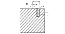
図1は本発明の第1の実施形態に係る平面アンテナの概略形状を示す図である。図1の平面アンテナは、地板1における所定の端辺2から所定形状に切り込まれて形成された切り込み部3を有する、いわゆるノッチアンテナであり、50Ωの給電線路に整合可能であることを特徴とする。
(First embodiment)
FIG. 1 is a diagram showing a schematic shape of a planar antenna according to the first embodiment of the present invention. The planar antenna shown in FIG. 1 is a so-called notch antenna having a
図1のノッチアンテナは、所定形状の切り込み部3が形成された地板1と、地板1と分離して切り込み部3の内部に配置される導体部4と、端辺2上に配置されて導体部4に給電点を行う給電点5と、端辺2上に配置されて地板1と導体部4とを電気的に分離する開放端6とを備えている。
The notch antenna of FIG. 1 includes a
導体部4は、地板1の一部を用いて形成されるが、地板1とは電気的に絶縁されている。地板1は、平面状の導体板からなり、導電性のよい材料であれば、どのような材料(例えば、銅、Alおよび鉄など)を用いてもよい。地板1は、導体と誘電体からなる誘電体基板でもよい。この場合、誘電体の誘電率を考慮してノッチアンテナの寸法を調整すればよい。導体板の代わりに、電気回路や無線回路等が搭載される回路基板を用いてもよい。回路基板が複数層で形成されており、接地として利用される導体層が存在する場合には、この導体層を地板1として利用してもよい。
The
なお、地板1の厚さは、使用する電波の波長に比べて十分に薄ければよく、例えば10分の1波長程度以下の厚さであれば特に制限はない。
In addition, the thickness of the
切り込み部3は、地板1上の導体が存在しない領域である。切り込みの幅は、地板1の厚さと同様に、使用する電波の波長に比べて十分に小さければよく、例えば10分の1波長程度以下の幅にすればよい。
The
給電点5は、切り込み部3の形成された地板1の端辺上に配置され、導電部に給電を行う。図2は給電点5の構造を詳細に示す斜視図であり、給電線路に同軸線路を用いる例を示している。同軸線路の外導体7は地板1に接地され、内導体8は導体部4に接続されている。このように、給電点5は、地板1と導体部4との間に電位差を与えるように給電を行う。図3は図2の地板1(導体板)を誘電体23の基板上に形成した例を示す図である。
The
給電線路として、同軸線路以外の線路(例えば、マイクロストリップ線路やコプレナー線路など)を用いることも可能である。同軸線路以外の線路を用いる場合も、同軸線路と同様の給電を行う。 As the feed line, a line other than the coaxial line (for example, a microstrip line or a coplanar line) can be used. When a line other than the coaxial line is used, the same power supply as that of the coaxial line is performed.
図4は、給電線路にマイクロストリップ線路26を用いた例を示している。導体板1の上に誘電体基板を設置し,その上にマイクロストリップ線路26が形成されている。マイクロストリップ線路26の一端は,高周波電源27に接続される。ここで,高周波電源27とは,マイクロストリップ線路26への給電点を表しており、マイクロストリップ線路26へ高周波信号を供給したり、マイクロストリップ線路26から入力される高周波信号を受信する。なお、高周波電源27は、図示していないが無線回路に接続される。マイクロストリップ線路26のもう一端は,給電点において導体板1(小さいほう)に接続される。その結果,導体板1(大きいほう)と導体板1(小さいほう)の間に電位差を与えることとなり、アンテナの給電点が形成される。なお、誘電体基板の大きさは大きくても小さくてもどちらでも良い。
FIG. 4 shows an example in which a
図2に戻り、導体部4を挟んで給電点5と対向配置される場所は開放端6であり、導体部4と地板1とが所定距離を隔てて対向配置されている。
Returning to FIG. 2, the place opposite to the
次に、図1のノッチアンテナの動作原理について説明する。まず、一般的なノッチアンテナが高インピーダンスになる理由について説明する。図5(a)は一般的なノッチアンテナの概略形状を示す図、図5(b)はノッチアンテナと電磁界的に補対となるモノポールアンテナの概略形状を示す図である。ここで、補対構造は、ノッチアンテナの切り込み9の形状とモノポールアンテナの素子10の形状が同一となる場合に成り立つものである。
Next, the operating principle of the notch antenna of FIG. 1 will be described. First, the reason why a general notch antenna has high impedance will be described. FIG. 5A is a diagram showing a schematic shape of a general notch antenna, and FIG. 5B is a diagram showing a schematic shape of a monopole antenna that is electromagnetically complemented with the notch antenna. Here, the complementary structure is established when the shape of the notch 9 of the notch antenna and the shape of the
図5(a)および図5(b)の形状において、ノッチアンテナの入力インピーダンスをZn、モノポールアンテナの入力インピーダンスをZmとする。このとき、補対関係にあるアンテナのインピーダンスの積は一定となる性質がある。なお、積の値は(60π)^2(Ω)である。これを式で表すと以下の(1)式で表される。 In the shapes of FIGS. 5A and 5B, the input impedance of the notch antenna is Zn, and the input impedance of the monopole antenna is Zm. At this time, the product of the impedances of the antennas in the complementary relationship has a property of being constant. The product value is (60π) ^ 2 (Ω). This is expressed by the following equation (1).
Zn×Zm=(60π)^2(Ω) …(1)
図5(b)に示すようなモノポールアンテナの入力インピーダンスは、共振周波数においてZm≒75Ω程度である。従って、図5(a)に示すノッチアンテナのインピーダンスはZn≒473Ωとなり、高インピーダンスになる。従って、ノッチアンテナは50Ωの給電線路には整合しない。.
なお、以上の補対の関係は、厳密には、地板1の大きさが無限の場合に成り立つ関係であり、有限の大きさの地板1だと、誤差が生じる。ただし、誤差が生じても、ノッチアンテナが高インピーダンスになることは変わらない。
Zn × Zm = (60π) ^ 2 (Ω) (1)
The input impedance of the monopole antenna as shown in FIG. 5B is about Zm≈75Ω at the resonance frequency. Therefore, the impedance of the notch antenna shown in FIG. 5A is Zn≈473Ω, which is a high impedance. Therefore, the notch antenna does not match the 50Ω feed line. .
Strictly speaking, the above complementary relationship is established when the size of the
ここで、本実施形態のノッチアンテナは、図1に示すような折り返し構造を採用している。図6は図1のノッチアンテナの補対構造を示す図である。図6に示す補対構造は、折り返しモノポールアンテナとなっている。折り返しモノポールアンテナは、モノポールアンテナの入力インピーダンスを大きくすることが出来るアンテナである。2本の線状素子20,21の太さと2本の線状素子20,21の間隔を調整することにより、モノポールアンテナのインピーダンスを1倍から50倍程度まで増加することが出来る。
Here, the notch antenna of the present embodiment employs a folded structure as shown in FIG. FIG. 6 is a diagram showing a complementary structure of the notch antenna of FIG. The complementary structure shown in FIG. 6 is a folded monopole antenna. The folded monopole antenna is an antenna that can increase the input impedance of the monopole antenna. By adjusting the thickness of the two
図1のアンテナと図6の折り返しモノポールアンテナとは補対の関係にあり、上述した(1)式の関係を満たすため、図6の折り返しモノポールアンテナのインピーダンスが大きくなるように調整すれば、その補対の構造である図1のアンテナのインピーダンスを下げることができる。 The antenna of FIG. 1 and the folded monopole antenna of FIG. 6 are in a complementary relationship, and in order to satisfy the relationship of the above-described equation (1), if the impedance of the folded monopole antenna of FIG. The impedance of the antenna of FIG. 1, which is the complementary structure, can be lowered.
より具体的には、図6の折り返しモノポールアンテナの入力インピーダンスを710Ω程度に調整し、その補対の構造になるように図1のアンテナの切り込み部3と導体部4を調整することにより、図1のアンテナのインピーダンスを50Ωの給電線路に整合させることができる。
More specifically, by adjusting the input impedance of the folded monopole antenna of FIG. 6 to about 710Ω and adjusting the
図7は本実施形態のノッチアンテナの入力インピーダンスをスミスチャート上に表した図である。この図はモーメント法の電磁界解析で求めた特性を示している。周波数は1.7〜2.7GHzの範囲を表し、スミスチャートの中心が50Ωの入力インピーダンスを表している。図7より、図1のノッチアンテナは、オフセット給電を行わなくても50Ωの給電線路に整合可能であることがわかる。 FIG. 7 is a diagram showing the input impedance of the notch antenna of the present embodiment on a Smith chart. This figure shows the characteristics obtained by the electromagnetic analysis of the moment method. The frequency represents a range of 1.7 to 2.7 GHz, and the center of the Smith chart represents an input impedance of 50Ω. From FIG. 7, it can be seen that the notch antenna of FIG. 1 can be matched to a 50Ω feed line without performing offset feed.
このように、本実施形態のノッチアンテナは、切り込み部3のみ折り返し構造にすることで、インピーダンスを下げることができ、インピーダンス変換回路などの別の回路を設けなくても、50Ωの給電線路に整合させることができ、構造を簡略化できて、コスト削減を図れる。
As described above, the notch antenna of the present embodiment can be reduced in impedance by making only the
図8は図1の第1の変形例を示すノッチアンテナの形状を示す図である。図8のノッチアンテナは、切り込み部3の形状がL字状であり、導体部4の形状も、切り込み部3の形状に沿ってL字状に形成されている。図8の構造の場合、切り込み部3の切り込み深さを短縮できるため、ノッチアンテナの小型化が可能となる。例えば、回路基板を用いて地板1を形成する場合、回路基板上の実装部品を避けて切り込み部3と導体部4を形成でき、アンテナ形状に対する制限を緩和できる。
FIG. 8 is a diagram showing the shape of a notch antenna showing a first modification of FIG. In the notch antenna of FIG. 8, the shape of the
なお、切り込み部3の形状は図1や図8に示すものに限定されず、図8よりもさらに複雑な形状の切り込み部3と導体部4を形成してもよい。
In addition, the shape of the
図9は図1の第2の変形例を示すノッチアンテナの形状を示す図である。図9のノッチアンテナは、切り込み部3が地板1の隣接する2辺に形成されており、導体部4も、切り込み部3の形状に沿って地板1の2辺に沿って形成されている。図9のノッチアンテナの場合、切り込み部3の端部に設けられる給電点5と開放端6が地板1の同一端辺上になく、隣接する2端辺上にある。また、切り込み部3と導体部4は直線状に形成されておらず、曲線で形成されている。したがって、切り込み部3の対向する2辺も平行ではない。図9のような形状であっても、切り込み部3のサイズと位置を調整することにより、50Ωの給電線路に整合させることが可能なインピーダンスに設定できる。
FIG. 9 is a diagram showing the shape of a notch antenna showing a second modification of FIG. In the notch antenna of FIG. 9, the
図8や図9のように切り込み部3の形状を種々変更することにより、放射パターンを制御することができる。この理由は、切り込みに沿って磁流が流れ、この磁流を波源として、放射パターンが決まるからである。
The radiation pattern can be controlled by variously changing the shape of the
(第2の実施形態)
第2の実施形態は、切り込み部3により切り取られる地板1の長さを、送受信される無線信号の波長の1/4(λ/4)に設定するものである。
(Second Embodiment)
In the second embodiment, the length of the
図10は本発明の第2の実施形態に係るノッチアンテナの概略形状を示す図である。図10のノッチアンテナは、基本的な形状は図1と同様であるが、切り込み部3により切り取られる地板1の長さを、送受信される無線信号の波長の1/4(λ/4)に設定している。
FIG. 10 is a diagram showing a schematic shape of a notch antenna according to the second embodiment of the present invention. The basic shape of the notch antenna of FIG. 10 is the same as that of FIG. 1, but the length of the
ここで、地板1の長さとは、切り込み部3が形成された地板1の端辺から測定した長さである。より具体的には、図1や図10のように長方形の切り込み部3の場合、地板1の端辺から切り込み部3の最深部までの長さであり、図8のようにL字状の切り込み部3の場合、地板1の端辺からL字に曲がった先の切り込み部3の最深部までの長さである。
Here, the length of the
本実施形態のノッチアンテナは、折り返しモノポールアンテナの補対構造であり、折り返しモノポールアンテナが共振するのは、モノポールの長さがλ/4となったときである。従って、本発明のノッチアンテナにおいても、折り返し構造の切り込みによって切り取られる地板1の長さをλ/4とすることで、動作周波数、言い換えれば、50Ωの給電線路に整合する周波数を設定することが可能となる。
The notch antenna of this embodiment is a complementary structure of a folded monopole antenna, and the folded monopole antenna resonates when the length of the monopole becomes λ / 4. Therefore, also in the notch antenna of the present invention, the operating frequency, in other words, the frequency matched to the 50Ω feed line can be set by setting the length of the
このように、第2実施形態では、切り込み部3により切り取られる地板1の長さを動作周波数の波長/4に設定することで、50Ωの給電線路に整合させつつ、所望の動作周波数で共振させることができる。従って、整合回路などを用いることなく、所望の動作周波数を設定でき、低コスト化および小型化が可能となる。
As described above, in the second embodiment, the length of the
モノポールアンテナは、λ/4の整数倍の長さが変化した場合でも、共振特性が発生する。従って、切り込み部3により切り取られる地板1の長さがλ/4×n(nは整数)であっても、同様に動作周波数の設定をすることが可能となる。このような長いノッチを用いると、アンテナが大きくなってしまうが、放射パターン制御や高利得化が実現しやすいなどの利点がある。
A monopole antenna exhibits resonance characteristics even when the length of an integral multiple of λ / 4 changes. Therefore, even if the length of the
なお、本実施形態では、折り返し構造の切り込みによって切り取られる地板1の長さをλ/4として説明してきた。この条件を別の見方で説明すると、給電点5から開放端6までの切り込みの全長がλ/4×2=λ/2となる条件とも等価である。従って、上述した図9に示すような曲線形状の切り込み部3を有する場合には、折り返し構造の切り込みの全長がλ/2となることが条件となる。
In the present embodiment, the length of the
(第3の実施形態)
第3の実施形態は、切り込み部3の内部に形成される導体部4と地板1との間隔を調整するものである。
(Third embodiment)
3rd Embodiment adjusts the space | interval of the
図11は本発明の第3の実施形態に係るノッチアンテナの概略形状を示す図であり、切り込み部3の周辺の構造を拡大表示したものである。図11のノッチアンテナは、切り込み部3の切り込み方向に伸びる導体部4の第1端辺と第2端辺のうち、第1端辺と地板1の対向配置される端辺との間隔11と、第2端辺と地板1の対向配置される端辺との間隔12とを、互いに相違させている。図11のような構造にし、両間隔11,12を調整することにより、50オームの給電線路に整合可能な入力インピーダンスが確実に得られる。以下に詳細に説明する。
FIG. 11 is a diagram showing a schematic shape of a notch antenna according to the third embodiment of the present invention, and is an enlarged view of the structure around the
図11のノッチアンテナは、折り返しモノポールアンテナと補対の関係にある。折り返しモノポールアンテナでは、インピーダンスを増大させるインピーダンス変換比を、平行な2本の線状素子それぞれの太さと2本の線状素子の素子間隔とによって調節することができる。従って、本実施形態の折り返しノッチアンテナにおいても、導体部4の両側に設けられる間隔11,12の幅を互いに変えることで、ノッチアンテナの入力インピーダンスを調節することが可能である。
The notch antenna of FIG. 11 is in a complementary relationship with the folded monopole antenna. In the folded monopole antenna, the impedance conversion ratio for increasing the impedance can be adjusted by the thickness of each of the two parallel linear elements and the element spacing of the two linear elements. Therefore, also in the folded notch antenna of the present embodiment, it is possible to adjust the input impedance of the notch antenna by changing the widths of the
図12は導体部4の両側の間隔11,12の幅と入力インピーダンスの抵抗値との関係の一例を示す図である。この値は、2GHz帯の周波数で導出したものである。なお、以下の(2)式の関係が成り立つ。
FIG. 12 is a diagram showing an example of the relationship between the width of the
間隔11の幅+導体の幅+間隔12の幅=一定の条件
図12に示すように、間隔11の幅を大きくすると抵抗値は高くなり、間隔12の幅を大きくすると抵抗値は低くなる。従って、間隔11,12の幅を変えることで、ノッチアンテナのインピーダンスを制御することができるようになる。
As shown in FIG. 12, when the width of the
なお、本実施形態の技術は、地板1の大きさが有限となる場合に有効である。このときには、折り返しモノポールアンテナと折り返しノッチアンテナの補対関係の誤差が大きくなり、折り返しノッチアンテナのインピーダンスを予測しにくい。このような場合に、特に有効となる。
In addition, the technique of this embodiment is effective when the magnitude | size of the
以上に説明したように、第3の実施形態では、切り込み部3の内部に形成された導体部4の両側に設けられる間隔11,12の幅を変えることによって、入力インピーダンスを調節することが出来る。従って、小型の地板1にノッチアンテナを設置した場合のインピーダンス変動を制御することができるようになる。
As described above, in the third embodiment, the input impedance can be adjusted by changing the widths of the
また、ノッチの形状を、例えばL 字のように、変形した場合にも、同様に、間隔11,12の幅を変えることで、インピーダンスを制御することが可能である。
Further, even when the shape of the notch is deformed, for example, like an L shape, the impedance can be controlled by changing the width of the
(第4の実施形態)
第4の実施形態は、給電点5を開放端6よりも地板1の端辺の中央寄りに設けるものである。図13は本発明の第4の実施形態に係るノッチアンテナの概略形状を示す図である。図13のノッチアンテナは、切り込み部3が形成された地板1の端辺の中央位置14の近くに給電点5を配置し、中央位置14から遠くに開放端6を配置している。このような構造により、有限サイズである小型の地板1の影響を少なくすることが可能となる。以下に詳細に説明する。
(Fourth embodiment)
In the fourth embodiment, the
図13のノッチアンテナでは、給電点5の近傍に強い電流分布を有する特徴がある。これは一般的なアンテナと同様であり、給電点5近傍の電流分布が一番強く、給電点5から離れるに従って、徐々に小さくなる。従って、給電点5近傍に十分な大きさの地板1が存在しない場合には、アンテナ性能が大幅に変化してしまう可能性がある。また、ノッチアンテナの補対関係の折り返しモノポールアンテナとの関係も大きく崩れることとなってしまう。
The notch antenna of FIG. 13 is characterized by having a strong current distribution in the vicinity of the
本実施形態のノッチアンテナでは、給電点5の配置される近傍の地板1のサイズが大きくなるように給電点5を配置している。したがって、有限地板1の影響を最小限にすることが可能となる。
In the notch antenna of the present embodiment, the
以上に説明したように、第4の実施形態によるノッチアンテナでは、給電点5と開放端6の相対的な配置位置を決定することによって、有限地板1の影響を最小限とし、有限地板1の影響で生じるアンテナ性能の変化を最小限にすることが可能である。
As described above, in the notch antenna according to the fourth embodiment, by determining the relative arrangement position of the
なお、切り込みの形状が変形している場合でも、同様に、給電点5と開放端6の相対的な位置を設定することで、同様な効果を得ることが出来る。
Even when the shape of the notch is deformed, the same effect can be obtained by setting the relative positions of the
(第5の実施形態)
第5の実施形態は、切り込み部3とは別個に、二次切り込み部を設けるものである。図14は本発明の第5の実施形態によるノッチアンテナの概略形状を示す図である。図14のノッチアンテナは、端辺に形成された二次切り込み部15を有する。このような二次切り込み部15を設けることにより、地板1上の電流分布を制御することができる。
(Fifth embodiment)
In the fifth embodiment, a secondary cut portion is provided separately from the
ノッチアンテナの特性は、切り込みに流れる磁流の特性で決定されるが、有限の地板1を用いた場合には、地板1上に流れる電流分布にも影響する。つまり、有限の大きさの地板1を用いた場合には、アンテナの入力インピーダンスや放射パターンが地板1上に存在する電流分布によって大きく影響を受けることとなる。これは、携帯無線機の小型化が進むと、特に問題となってくる。
The characteristics of the notch antenna are determined by the characteristics of the magnetic current flowing through the notch, but when the
本実施形態では、地板1に二次切り込み部15を設けることにより、地板1上の電流分布を制御し、これにより、アンテナの入力インピーダンスや放射パターンといった特性を可変することができる。なお、二次切り込み部15を設ける場所は、特に問わないが、地板1の端辺から切り込んで二次切り込み部15を形成するのが望ましい。
In this embodiment, by providing the
ここで、地板1上の電流は、地板1の周辺部、つまり、地板1の辺に近い部分に強く存在している。従って、本実施形態のように、地板1の端辺から切り込まれた二次切り込み部15を設けると、地板1上の電流分布を大幅に変更でき、アンテナの入力インピーダンスや、放射パターンといった特性を制御できるようになる。
Here, the current on the
以上に説明したように、第5の実施形態では、地板1の端辺から切り込まれた二次切り込み部15を設けるため、地板1上の電流分布を制御し、アンテナ特性を制御できるようになる。なお、二次切り込み部15の形状に関する制限は無い。また、二次切り込み部15を地板1の複数箇所に設けて、アンテナ特性の制御を行ってもよい。
As described above, in the fifth embodiment, since the
(第6の実施形態)
第6の実施形態は、第5の実施形態の変形例であり、二次切り込み部を設ける場所を特定するものである。
(Sixth embodiment)
The sixth embodiment is a modification of the fifth embodiment and specifies a place where the secondary cut portion is provided.
図15は本発明の第6の実施形態に係るノッチアンテナの概略形状を示す図である。図15のノッチアンテナは、開放端6に隣接する地板1の辺に二次切り込み部15を設けている。このような構造により、ノッチアンテナを広帯域化することが可能となる。以下、詳細に説明する。
FIG. 15 is a diagram showing a schematic shape of a notch antenna according to the sixth embodiment of the present invention. The notch antenna of FIG. 15 is provided with a
本実施形態の二次切り込み部15は、切り込み部3の開放端6に隣接する地板1の端辺上に設けられ、地板1上の電流分布を制御する。このような電流分布の制御を行うことで、広帯域特性を有する自己補対アンテナの電流分布に類似することになる。従って、ノッチアンテナの広帯域特性が実現できる。
The
図16は自己補対アンテナの概略形状を示す図である。図16のアンテナは、図1のノッチアンテナを、給電点5と開放端6の位置する地板1の端辺を軸として180度回転させた構造になっている。したがって、図1のアンテナは、図16の自己補対アンテナの変形であるともみなせる。
FIG. 16 is a diagram showing a schematic shape of a self-complementary antenna. The antenna of FIG. 16 has a structure in which the notch antenna of FIG. 1 is rotated 180 degrees around the end side of the
自己補対アンテナは一般に、インピーダンスの広帯域特性を有するアンテナとしてよく知られている。従って、自己補対アンテナに類似した特徴を持たせることで、帯域幅特性を広くすることが出来ると考えられる。 A self-complementary antenna is generally well known as an antenna having a broadband characteristic of impedance. Therefore, it can be considered that the bandwidth characteristics can be widened by providing characteristics similar to those of the self-complementary antenna.
そこで、図1のアンテナと図16の自己補対アンテナとの類似度を調べる評価方法として、アンテナ特性を決定する地板1上の電流分布の比較を行った。その結果、図17に示すような特性が得られた。
Therefore, as an evaluation method for examining the similarity between the antenna of FIG. 1 and the self-complementary antenna of FIG. 16, the current distribution on the
図17(b)は図16のアンテナにおける端辺ABの電流振幅特性図、図17(c)は図16の端辺ABの電流位相特性図である。また、図17(e)は図1のアンテナにおける端辺ABの電流振幅特性図、図17(f)は図1のアンテナにおける端辺ABの電流位相特性図である。ここで、端辺ABは、切り込み部3が形成された地板1の端辺に隣接する端辺である。
17B is a current amplitude characteristic diagram of the edge AB in the antenna of FIG. 16, and FIG. 17C is a current phase characteristic diagram of the edge AB of FIG. FIG. 17E is a current amplitude characteristic diagram of the edge AB in the antenna of FIG. 1, and FIG. 17F is a current phase characteristic diagram of the edge AB of the antenna of FIG. Here, the end side AB is an end side adjacent to the end side of the
ここで、切り込み部3の開放端6の位置する端辺に隣接する端辺ABの電流分布を調べる理由は、開放端6に隣接する辺において、最も電流分布に大きな違いがあるためである。電流振幅は正規化して示してある。電流位相のグラフは、縦軸の位相のメモリを全てのグラフで同じにしているので、相対的に比較できるようにしている。
Here, the reason why the current distribution of the edge AB adjacent to the edge where the
図16に示す自己補対アンテナの場合、電流の振幅が小さくなる部分が辺の中央付近に存在している。また、その電流振幅の小さくなる部分の前後で、電流位相が大きく変化していることもわかる。
一方、図1に示す折り返し構造を有するノッチアンテナの場合、端辺の中央付近に電流の振幅が急激に小さくなる部分が存在していない。また、電流位相もなだらかに変化する分布になっている。
In the case of the self-complementary antenna shown in FIG. 16, a portion where the current amplitude is small exists near the center of the side. It can also be seen that the current phase changes greatly before and after the portion where the current amplitude becomes small.
On the other hand, in the case of the notch antenna having the folded structure shown in FIG. 1, there is no portion in which the amplitude of the current decreases rapidly near the center of the edge. Also, the current phase has a distribution that changes gently.
以上のように、図1に示す折り返し構造を有するノッチアンテナは、図16に示す自己補対アンテナの放射素子を折り曲げただけの構造であるが、地板1上の電流分布は異なり、従って、自己補対アンテナと同様の広帯域特性が得られないおそれがある。
As described above, the notch antenna having the folded structure shown in FIG. 1 has a structure in which the radiating element of the self-complementary antenna shown in FIG. 16 is simply bent, but the current distribution on the
そこで、本実施形態では、図15に示すように、開放端6に隣接する地板1の辺に二次切り込み部15を設け、電流分布の制御を行っている。
Therefore, in the present embodiment, as shown in FIG. 15, a
図18は、二次切り込み部15を設けた効果を示すために、切り込みの長さに対する周波数帯域幅を示す図である。ここで、周波数帯域幅は、VSWRが2以下となる帯域幅として定義している。
FIG. 18 is a diagram showing the frequency bandwidth with respect to the length of the cut in order to show the effect of providing the
なお、VSWRは、給電線路の特性インピーダンスを50Ωとした場合で評価している。VSWRが2以下の場合とは、給電線路とアンテナとの不整合損が0.5dB以下となる範囲であり、アンテナの動作範囲としてよく使用される値である.図18より、切り込みの長さが0mmに対して、切り込み長さ30mmとすることで、帯域幅は約1.5倍と広帯域化が実現できていることがわかる。 VSWR is evaluated when the characteristic impedance of the feeder line is 50Ω. The case where the VSWR is 2 or less is a range in which the mismatch loss between the feed line and the antenna is 0.5 dB or less, which is a value often used as the operating range of the antenna. It can be seen that by setting the cut length to 30 mm with respect to 0 mm, the bandwidth can be increased to about 1.5 times.
二次切り込み部15の切り込み長さは、アンテナの設置位置や、アンテナ形状、地板1の大きさなどによっても影響を受ける。ただし、切り込みの長さをλ/4程度とすることで、切り込みの部分に大きな電流分布の変化が発生し、大幅な特性改善が期待できる。
The cut length of the
また、切り込みの形状は、任意の形状を採用することが可能である。ここでは、長方形の切り込みの形状を用いた。L字の形状であっても、曲線状の形状であっても、同様な効果が期待できる。 Further, any shape can be adopted as the shape of the cut. Here, a rectangular cut shape was used. The same effect can be expected regardless of the L shape or the curved shape.
図19は開放端6の形成された地板1の端辺に隣接する端辺に二次切り込み部15を設けた場合の電流分布を示す図である。ここでは、広帯域化が実現されている場合の電流分布である。図19(b)は図19(a)の端辺AB(開放端6が形成された端辺に隣接する端辺)における電流振幅特性図、図19(c)は端辺ABにおける電流位相特性図である。
FIG. 19 is a diagram showing a current distribution when the
図17の自己補対アンテナの電流分布と比較すると、電流振幅は辺の中央付近で小さくなり、自己補対アンテナの電流振幅に類似する。また、位相分布は、辺の中央付近で急激に変化している点も類似している。従って、図15のノッチアンテナは、図1のノッチアンテナに二次切り込み部15を設けることにより、図16の自己補対アンテナの電流分布に類似した特性が得られる。その結果、自己補対アンテナと同様の広帯域特性が得られ、周波数帯域幅特性が改善されたといえる。
Compared with the current distribution of the self-complementary antenna in FIG. 17, the current amplitude is smaller near the center of the side and is similar to the current amplitude of the self-complementary antenna. The phase distribution is also similar in that it changes rapidly near the center of the side. Therefore, the notch antenna of FIG. 15 has characteristics similar to the current distribution of the self-complementary antenna of FIG. 16 by providing the
以上に説明したように、第6の実施形態の自己補対アンテナでは、二次切り込み部15を開放端6の形成された地板1の端辺に隣接する端辺に設けるため、自己補対アンテナに類似した電流分布特性が得られる。その結果、本実施形態のノッチアンテナの広帯域化が実現される。
As described above, in the self-complementary antenna of the sixth embodiment, the
また、平面構造で広帯域特性を実現するため、携帯無線機の小型化が可能である。さらに、二次切り込み部15を設けるだけで、他に何も加工等を行わなくてよいため、ノッチアンテナの切り込みと同様に製造でき、低コスト化が可能である。また、切り込みを入れることにより、アンテナの軽量化が可能となる。また、広帯域特性が実現されるので、地上波TV受信、UWB(Ultra Wide Band)などの広帯域システムへの適用が可能となる。
Further, since the broadband structure is realized with the planar structure, the portable radio can be miniaturized. Furthermore, since only the
なお、以上の説明は、地板1の形状が長方形の場合で説明を行ったが、任意の形状の地板1にも適用することが可能である。
In addition, although the above description demonstrated in the case where the shape of the
また、切り込み部3は、何も存在しない部分として説明してきたが、切り込み部3に電気的に空気に近い媒質定数の物質を充填してアンテナ部分を固定することが可能である。これにより、携帯無線機の落下に対するアンテナの故障に耐性を持たせることも可能である。また、切り込み部3に誘電体や磁性体を用いることもできる。この場合、切り込みを流れる磁流の波長短縮が生じるので、誘電率、あるいは、透磁率にあわせて、切り込みの長さを調節すればよい
この他、本実施形態のアンテナを地板1に2つ以上搭載し、ダイバーシチやアダプティブアンテナとして用いることも出来る。2つ以上のアンテナを同一平面状に構成することが可能であり、小型化に有効である。また、MIMO(Multiple Input Multiple Output)においても、本実施形態の平面アンテナを用いて複数のアンテナを構築すれば、小型化が可能となる。
Although the
また、車、電車、飛行機などでは、移動に伴うアンテナの破損を回避するために、内蔵アンテナが要求される場合が多い。そこで、本実施形態のノッチアンテナを用いることで、十分小型な内蔵アンテナを実現することが可能である。 In addition, cars, trains, airplanes, and the like often require a built-in antenna to avoid damage to the antenna due to movement. Thus, a sufficiently small built-in antenna can be realized by using the notch antenna of the present embodiment.
また、人体に密着させて使用する無線タグ用のアンテナは、薄型化が要求されるため、本実施形態のアンテナを用いることは有効である。また、この場合、地板1を湾曲させることで、人体の形状に合わせて密着してアンテナを装着することが可能であり、アンテナが人体から突起しない形状となり、非常に有効となる。なお、人体に密着させて使用する場合には、人体とアンテナの干渉によって、アンテナ特性が変化する場合がある。これを回避するためには、あらかじめ人体がある前提でアンテナを設計すればよい。あるいは、アンテナと人体の間に導体板や誘電体板などを配置して、人体の影響を軽減することが望ましい。
Further, since the RFID tag antenna used in close contact with the human body is required to be thin, it is effective to use the antenna of this embodiment. In this case, by bending the
また、本発明は、放射特性を電気的に可変なチューナブルアンテナへの応用も可能である。チューナブルアンテナとは、アンテナの一部に電気特性可変素子を有し、その可変素子を制御することによって、放射パターンや、入力インピーダンスといったアンテナ特性を可変させることが可能なものをいう。 The present invention can also be applied to a tunable antenna whose radiation characteristics are electrically variable. A tunable antenna has an electric characteristic variable element in a part of the antenna and can control antenna characteristics such as a radiation pattern and input impedance by controlling the variable element.
ここで、可変素子とは、高周波スイッチ、可変容量、可変インダクタンス、可変抵抗など、任意の可変素子、および、受動素子の組み合わせで実現することが可能である。なお、これらの可変素子は、半導体素子やMEMSなどを用いて構成しても良い。 Here, the variable element can be realized by a combination of an arbitrary variable element such as a high-frequency switch, a variable capacitor, a variable inductance, and a variable resistor, and a passive element. Note that these variable elements may be configured using semiconductor elements, MEMS, or the like.
本実施形態のノッチアンテナでは、切り込みの一部に可変素子を取り付けることでアンテナ特性を可変することが可能となる。ここで、アンテナが地板1上に形成されているので、可変素子を同一平面状に構成することが出来る。従って、可変素子を取り付けるためのほかの部品を必要としない。また、可変素子を取り付けても、平面でアンテナを構成することが出来るといった特徴を有する。
In the notch antenna of this embodiment, it is possible to vary the antenna characteristics by attaching a variable element to a part of the cut. Here, since the antenna is formed on the
なお、本実施形態は上記実施形態そのままに限定されるものではなく、実施段階ではその要旨を逸脱しない範囲で構成要素を変形して具体化できる。また、上記実施形態に開示されている複数の構成要素の適宜な組み合わせにより、種々の発明を形成できる。例えば、実施形態に示される全構成要素から幾つかの構成要素を削除してもよい。さらに、異なる実施形態にわたる構成要素を適宜組み合わせてもよい。 Note that the present embodiment is not limited to the above-described embodiment as it is, and can be embodied by modifying the components without departing from the scope of the invention in the implementation stage. In addition, various inventions can be formed by appropriately combining a plurality of components disclosed in the embodiment. For example, some components may be deleted from all the components shown in the embodiment. Furthermore, constituent elements over different embodiments may be appropriately combined.
1 地板
2 端辺
3 切り込み部
4 導体部
5 給電点
6 開放端
15 二次切り込み部
DESCRIPTION OF
Claims (10)
前記切り込み部の形状に沿って前記第1の導体板と分離して形成される第2の導体板と、
前記切り込み部の形成された前記第1の導体板の端辺上に配置され、前記第2の導体板に給電を行う給電点と、
前記切り込み部の形成された前記第1の導体板の端辺上に配置され、前記第1および第2の導体板を電気的に分離する開放端と、を備えることを特徴とする平面アンテナ。 A first conductor plate having a cut portion formed by cutting into a predetermined shape from at least one end side;
A second conductor plate formed separately from the first conductor plate along the shape of the notch,
A feeding point that is disposed on an edge of the first conductor plate in which the cut portion is formed and feeds power to the second conductor plate;
A planar antenna, comprising: an open end that is disposed on an end side of the first conductive plate in which the cut portion is formed and electrically separates the first and second conductive plates.
Priority Applications (1)
| Application Number | Priority Date | Filing Date | Title |
|---|---|---|---|
| JP2004328044A JP2006140735A (en) | 2004-11-11 | 2004-11-11 | Planar antenna |
Applications Claiming Priority (1)
| Application Number | Priority Date | Filing Date | Title |
|---|---|---|---|
| JP2004328044A JP2006140735A (en) | 2004-11-11 | 2004-11-11 | Planar antenna |
Publications (1)
| Publication Number | Publication Date |
|---|---|
| JP2006140735A true JP2006140735A (en) | 2006-06-01 |
Family
ID=36621228
Family Applications (1)
| Application Number | Title | Priority Date | Filing Date |
|---|---|---|---|
| JP2004328044A Pending JP2006140735A (en) | 2004-11-11 | 2004-11-11 | Planar antenna |
Country Status (1)
| Country | Link |
|---|---|
| JP (1) | JP2006140735A (en) |
Cited By (12)
| Publication number | Priority date | Publication date | Assignee | Title |
|---|---|---|---|---|
| EP2031698A1 (en) | 2007-08-30 | 2009-03-04 | Fujitsu Limited | Tag antenna and tag |
| JP2010028569A (en) * | 2008-07-22 | 2010-02-04 | Samsung Electronics Co Ltd | Antenna apparatus |
| WO2010116589A1 (en) * | 2009-03-30 | 2010-10-14 | 日本電気株式会社 | Slot antenna, electronic apparatus, and method for manufacturing slot antenna |
| JP2012105134A (en) * | 2010-11-11 | 2012-05-31 | Fujitsu Ltd | Radio equipment and antenna device |
| US8570173B2 (en) | 2007-07-25 | 2013-10-29 | Fujitsu Limited | Radio frequency tag and method of manufacturing the same |
| CN103531912A (en) * | 2013-10-10 | 2014-01-22 | 深圳市维力谷无线技术有限公司 | Folding type slot antenna |
| WO2014129588A1 (en) * | 2013-02-21 | 2014-08-28 | 旭硝子株式会社 | Vehicular window glass, and antenna |
| US8991716B2 (en) | 2011-07-20 | 2015-03-31 | Fujikura Ltd. | Antenna and wireless tag |
| CN106663875A (en) * | 2015-05-28 | 2017-05-10 | 华为技术有限公司 | Slot antenna and electronic device |
| CN108258387A (en) * | 2016-12-28 | 2018-07-06 | 上海圣丹纳电子科技股份有限公司 | A kind of mobile unit antenna of closed loop configuration |
| CN109742511A (en) * | 2018-12-14 | 2019-05-10 | 惠州Tcl移动通信有限公司 | A kind of communication terminal and its antenna structure |
| US11367963B2 (en) | 2018-04-13 | 2022-06-21 | Murata Manufacturing Co., Ltd. | Antenna device |
-
2004
- 2004-11-11 JP JP2004328044A patent/JP2006140735A/en active Pending
Cited By (26)
| Publication number | Priority date | Publication date | Assignee | Title |
|---|---|---|---|---|
| US8570173B2 (en) | 2007-07-25 | 2013-10-29 | Fujitsu Limited | Radio frequency tag and method of manufacturing the same |
| US7859414B2 (en) | 2007-08-30 | 2010-12-28 | Fujitsu Limited | Tag antenna and tag |
| EP2031698A1 (en) | 2007-08-30 | 2009-03-04 | Fujitsu Limited | Tag antenna and tag |
| JP2010028569A (en) * | 2008-07-22 | 2010-02-04 | Samsung Electronics Co Ltd | Antenna apparatus |
| CN102349196B (en) * | 2009-03-30 | 2014-10-22 | 日本电气株式会社 | Slot antenna, electronic apparatus, and method for manufacturing slot antenna |
| WO2010116589A1 (en) * | 2009-03-30 | 2010-10-14 | 日本電気株式会社 | Slot antenna, electronic apparatus, and method for manufacturing slot antenna |
| CN102349196A (en) * | 2009-03-30 | 2012-02-08 | 日本电气株式会社 | Slot antenna, electronic apparatus, and method for manufacturing slot antenna |
| JP5477377B2 (en) * | 2009-03-30 | 2014-04-23 | 日本電気株式会社 | Slot antenna, electronic device, and method for manufacturing slot antenna |
| US8982003B2 (en) | 2009-03-30 | 2015-03-17 | Nec Corporation | Slot antenna, electronic apparatus, and method for manufacturing slot antenna |
| JP2012105134A (en) * | 2010-11-11 | 2012-05-31 | Fujitsu Ltd | Radio equipment and antenna device |
| US8991716B2 (en) | 2011-07-20 | 2015-03-31 | Fujikura Ltd. | Antenna and wireless tag |
| WO2014129588A1 (en) * | 2013-02-21 | 2014-08-28 | 旭硝子株式会社 | Vehicular window glass, and antenna |
| US9509038B2 (en) | 2013-02-21 | 2016-11-29 | Asahi Glass Company, Limited | Vehicle window glass and antenna |
| JPWO2014129588A1 (en) * | 2013-02-21 | 2017-02-02 | 旭硝子株式会社 | Vehicle window glass and antenna |
| CN103531912A (en) * | 2013-10-10 | 2014-01-22 | 深圳市维力谷无线技术有限公司 | Folding type slot antenna |
| CN103531912B (en) * | 2013-10-10 | 2016-08-17 | 深圳市维力谷无线技术股份有限公司 | A kind of collapsible slot antenna |
| EP3291373A4 (en) * | 2015-05-28 | 2018-04-25 | Huawei Technologies Co., Ltd. | Slot antenna and electronic device |
| CN106663875A (en) * | 2015-05-28 | 2017-05-10 | 华为技术有限公司 | Slot antenna and electronic device |
| CN106663875B (en) * | 2015-05-28 | 2019-09-03 | 华为技术有限公司 | Slot antenna and electronic equipment |
| US10811780B2 (en) | 2015-05-28 | 2020-10-20 | Huawei Technologies Co., Ltd. | Slot antenna and electronic device |
| US11380999B2 (en) | 2015-05-28 | 2022-07-05 | Huawei Technologies Co., Ltd. | Slot antenna and electronic device |
| CN108258387A (en) * | 2016-12-28 | 2018-07-06 | 上海圣丹纳电子科技股份有限公司 | A kind of mobile unit antenna of closed loop configuration |
| CN108258387B (en) * | 2016-12-28 | 2023-09-05 | 上海圣丹纳无线科技有限公司 | Vehicle-mounted equipment antenna with closed-loop structure |
| US11367963B2 (en) | 2018-04-13 | 2022-06-21 | Murata Manufacturing Co., Ltd. | Antenna device |
| CN109742511A (en) * | 2018-12-14 | 2019-05-10 | 惠州Tcl移动通信有限公司 | A kind of communication terminal and its antenna structure |
| CN109742511B (en) * | 2018-12-14 | 2021-01-26 | 惠州Tcl移动通信有限公司 | Mobile communication terminal and antenna structure thereof |
Similar Documents
| Publication | Publication Date | Title |
|---|---|---|
| EP3245691B1 (en) | Low common mode resonance multiband radiating array | |
| US7164387B2 (en) | Compact tunable antenna | |
| JP5009240B2 (en) | Multiband antenna and wireless communication terminal | |
| US6844853B2 (en) | Dual band antenna for wireless communication | |
| US20170077599A1 (en) | Multi-antenna and radio apparatus including thereof | |
| CN102017292B (en) | Broadband built-in antenna using a slow wave structure | |
| EP2602865B1 (en) | Multi-band antenna | |
| US9660347B2 (en) | Printed coupled-fed multi-band antenna and electronic system | |
| US20140062794A1 (en) | Broadband Multi-Strip Patch Antenna | |
| US7170456B2 (en) | Dielectric chip antenna structure | |
| JP2009111999A (en) | Multiband antenna | |
| US20060284770A1 (en) | Compact dual band antenna having common elements and common feed | |
| CN103081220A (en) | Antenna device and wireless communication apparatus | |
| JP2012528531A (en) | Method for reducing near field radiation and specific absorptance (SAR) values of communication devices | |
| JP2006140735A (en) | Planar antenna | |
| JP6624650B2 (en) | antenna | |
| Mopidevi et al. | A quad-band antenna for public safety applications | |
| KR20090096914A (en) | Planar folded monopole antenna | |
| JP4431360B2 (en) | Multiband antenna | |
| KR100985840B1 (en) | Multi band wifi antenna | |
| Hamid et al. | Wideband reconfigurable log periodic patch array | |
| US11239560B2 (en) | Ultra wide band antenna | |
| CN108428999B (en) | Antenna with a shield | |
| Zhang et al. | A novel pattern reconfigurable wideband slot antenna using PIN diodes | |
| Abdollahvand et al. | Compact band-rejection printed monopole antenna for UWB application |
Legal Events
| Date | Code | Title | Description |
|---|---|---|---|
| A977 | Report on retrieval |
Effective date: 20070625 Free format text: JAPANESE INTERMEDIATE CODE: A971007 |
|
| A131 | Notification of reasons for refusal |
Free format text: JAPANESE INTERMEDIATE CODE: A131 Effective date: 20070629 |
|
| A521 | Written amendment |
Effective date: 20070828 Free format text: JAPANESE INTERMEDIATE CODE: A523 |
|
| A02 | Decision of refusal |
Free format text: JAPANESE INTERMEDIATE CODE: A02 Effective date: 20070918 |