JP2006040484A - Flash memory module - Google Patents
Flash memory module Download PDFInfo
- Publication number
- JP2006040484A JP2006040484A JP2004222375A JP2004222375A JP2006040484A JP 2006040484 A JP2006040484 A JP 2006040484A JP 2004222375 A JP2004222375 A JP 2004222375A JP 2004222375 A JP2004222375 A JP 2004222375A JP 2006040484 A JP2006040484 A JP 2006040484A
- Authority
- JP
- Japan
- Prior art keywords
- flash memory
- block
- data
- connector
- memory module
- Prior art date
- Legal status (The legal status is an assumption and is not a legal conclusion. Google has not performed a legal analysis and makes no representation as to the accuracy of the status listed.)
- Withdrawn
Links
- 230000015654 memory Effects 0.000 title claims abstract description 158
- 239000000758 substrate Substances 0.000 claims abstract description 20
- 238000006243 chemical reaction Methods 0.000 description 20
- 238000000034 method Methods 0.000 description 13
- 238000010586 diagram Methods 0.000 description 7
- 230000002950 deficient Effects 0.000 description 4
- 230000007257 malfunction Effects 0.000 description 3
- 239000004065 semiconductor Substances 0.000 description 2
- XUIMIQQOPSSXEZ-UHFFFAOYSA-N Silicon Chemical compound [Si] XUIMIQQOPSSXEZ-UHFFFAOYSA-N 0.000 description 1
- 230000007423 decrease Effects 0.000 description 1
- 238000007599 discharging Methods 0.000 description 1
- 230000000694 effects Effects 0.000 description 1
- 230000006870 function Effects 0.000 description 1
- 230000010365 information processing Effects 0.000 description 1
- 238000007689 inspection Methods 0.000 description 1
- 239000012212 insulator Substances 0.000 description 1
- 230000000717 retained effect Effects 0.000 description 1
- 229910052710 silicon Inorganic materials 0.000 description 1
- 239000010703 silicon Substances 0.000 description 1
- 230000003068 static effect Effects 0.000 description 1
Images


Abstract
Description
本発明は、フラッシュメモリモジュールに関する。 The present invention relates to a flash memory module.
近年、メモリーカードやシリコンディスク等の形態でメモリシステムに使用される半導体メモリとして、フラッシュメモリが広く採用されている。フラッシュメモリに格納されたデータは、電力が供給されていないときでも保持されていることが要求される。 In recent years, flash memory has been widely adopted as a semiconductor memory used in a memory system in the form of a memory card, a silicon disk, or the like. Data stored in the flash memory is required to be retained even when power is not supplied.
NAND型フラッシュメモリは、上記のメモリシステムで特に多く用いられるフラッシュメモリである。
NAND型フラッシュメモリに含まれている複数のメモリセルのそれぞれは、消去状態のときに論理値“1”を示し、書込み状態の時に“0”を示す。そして、複数のメモリセルは、他のメモリセルとは独立して消去状態から書込状態へと変化することができる。
The NAND flash memory is a flash memory that is particularly frequently used in the above memory system.
Each of the plurality of memory cells included in the NAND flash memory indicates a logical value “1” when in an erased state and indicates “0” when in a written state. The plurality of memory cells can change from the erased state to the written state independently of other memory cells.
これとは対照的に、書込状態から消去状態へと変化させるときには、各メモリセルは他のメモリセルと独立して変化させることができない。この書込状態から消去状態に変化させるときには、ブロックと称される予め定められた所定数のメモリセルを全て同時に消去状態にする。この一括消去動作は、一般的に、「ブロック消去」と称されている。NAND型フラッシュメモリに対する書込処理若しくは読出処理は、ページと称される予め定められた数のメモリセル単位に処理が行なわれる。消去処理の単位であるブロックは複数のページで構成されている。 In contrast, when changing from the written state to the erased state, each memory cell cannot be changed independently of the other memory cells. When changing from the written state to the erased state, all of a predetermined number of memory cells called blocks are simultaneously erased. This collective erasure operation is generally called “block erase”. The writing process or the reading process for the NAND flash memory is performed in units of a predetermined number of memory cells called pages. A block which is a unit of erasure processing is composed of a plurality of pages.
又、フラッシュメモリには寿命があり、消去処理と書込処理が繰り返される書替の回数が増大すると、正常な書込みを行なうことができない不良ブロックが発生する。この不良ブロックの数が増えると、フラッシュメモリの信頼性が低下し、使用し続けることが困難になる。従って、フラッシュメモリは、通常、ホストシステムの基板に実装して使用されず、各種の外部インターフェースコネクタを介して接続される外部記憶メディアとして使用されている。 Further, the flash memory has a lifetime, and when the number of rewrites in which the erasure process and the write process are repeated increases, a defective block in which normal writing cannot be performed occurs. As the number of defective blocks increases, the reliability of the flash memory decreases and it becomes difficult to keep using it. Therefore, the flash memory is normally not used by being mounted on a host system board, but is used as an external storage medium connected via various external interface connectors.
下記特許文献1では、コンパクトフラッシュ(登録商標)でありながら、スマートメディアとしても利用できる外部記憶メディアが提案されている。
フラッシュメモリに、ブートプログラムやドライバプログラム等を記憶して、ホストシステム内に内臓して使用したい場合がある。しかしながら、特許文献1に示されているコンパクトフラッシュ(登録商標)やスマートメディアは、外部記憶メディアとして使用することはできるが、ホストシステム内に内臓して使用することはできなかった。
There are cases in which a boot program, a driver program, or the like is stored in a flash memory and used in a host system. However, although CompactFlash (registered trademark) and smart media disclosed in
本発明は、ホストシステム内に内臓して使用するのに好適なフラッシュメモリモジュールを提供することを目的とする。 An object of the present invention is to provide a flash memory module suitable for use in a host system.
上記目的を達成するために、本発明の観点に係るフラッシュメモリモジュールは、ホストシステムの持つバスに電気的に接続されるコネクタと、フラッシュメモリと、前記フラッシュメモリに接続され、前記コネクタを介して前記バスから与えられる書込み命令若しくは読出し命令に基づいて該フラッシュメモリに対するアクセスを制御する制御回路と、前記コネクタ、前記制御回路及び前記フラッシュメモリが実装された基板と、を備えることを特徴とする。 In order to achieve the above object, a flash memory module according to an aspect of the present invention includes a connector electrically connected to a bus of a host system, a flash memory, and the flash memory. A control circuit that controls access to the flash memory based on a write command or a read command given from the bus, and a board on which the connector, the control circuit, and the flash memory are mounted.
なお、前記コネクタを介して供給される電源の電圧値を検出する手段と、前記電圧値が予め設定された電圧値に達するまで、前記制御回路を停止状態にする起動制御回路と、を備えてもよい。 A means for detecting a voltage value of the power supplied via the connector; and a start control circuit for stopping the control circuit until the voltage value reaches a preset voltage value. Also good.
又、前記コネクタが前記バスに接続されることにより、前記基板が前記ホストシステムの内部の主基板に実装され、該基板と該主基板とが対向するようにしてもよい。 Further, by connecting the connector to the bus, the board may be mounted on a main board inside the host system so that the board and the main board face each other.
又、前記制御回路の少なくとも一部と前記フラッシュメモリとが、前記基板の互いに異なる面に実装されてもよい。 Further, at least a part of the control circuit and the flash memory may be mounted on different surfaces of the substrate.
本発明のフラッシュメモリモジュールは、コネクタを介してホストシステム内の主基板に実装することができるので、ブートプログラムやドライバプログラム等を記憶したフラッシュメモリモジュールを、ホストシステム内に容易に内蔵させることができる。又、コネクタを介して実装されているので、不良ブロックの増加等の不具合が生じた場合であっても、容易に交換することができる。更に、フラッシュメモリモジュールの初期化等を別の装置で行なった後に、ホストシステム内の主基板に実装することもできる。 Since the flash memory module of the present invention can be mounted on a main board in a host system via a connector, a flash memory module storing a boot program, a driver program, etc. can be easily incorporated in the host system. it can. Moreover, since it is mounted via a connector, it can be easily replaced even if a problem such as an increase in defective blocks occurs. Furthermore, after the initialization of the flash memory module or the like is performed by another device, it can be mounted on the main board in the host system.
以下、図面に基づき、本発明の実施形態について説明する。
図1は、本発明の実施形態に係るフラッシュメモリモジュール1を概略的に示す機能ブロック図である。
図2は、フラッシュメモリモジュールの外形を示す図である。
Hereinafter, embodiments of the present invention will be described with reference to the drawings.
FIG. 1 is a functional block diagram schematically showing a
FIG. 2 is a view showing the outer shape of the flash memory module.
図1のように、フラッシュメモリモジュール1は、NAND型フラッシュメモリで構成されたフラッシュメモリ2と、フラッシュメモリ2を制御するメモリコントローラ3とを備えている。
As shown in FIG. 1, the
フラッシュメモリモジュール1は、図2(b)に示したようにホストシステム内の主基板16にコネクタ14aを介して実装され、ホストシステム内に内蔵された記憶装置として用いられる。フラッシュメモリモジュール1は、外部インターフェースコネクタに接続される記憶メディアとは異なり、頻繁に抜差しされることがないため、ブートプログラムやドライバプログラム等のプログラムやホストシステムで頻繁使用されるデータ等を保存する用途に適している。
As shown in FIG. 2B, the
フラッシュメモリモジュール1は、図2(a)に示したように、基板15の一方の面にフラッシュメモリ2が実装され、他方の面にメモリコントローラ3が実装されている。このように、フラッシュメモリ2とメモリコントローラ3を異なる面に実装することにより、基板15の面積を小さくすることができる。
As shown in FIG. 2A, the
基板15のメモリコントローラ3が実装されている面には、ホストシステム内の主基板16と接続するためのコネクタ14aが実装されている。ホストシステム内の主基板16には、フラッシュメモリモジュール1の基板15に実装されているコネクタ14aと接続するコネクタ14bが実装されている。このコネクタ14bは、フラッシュメモリモジュール1内のATAバス4に接続されている。従って、コネクタ14aとコネクタ14bが接続されることにより、フラッシュメモリモジュール1は、ホストシステム内のATAバス4に接続される。
A
基板15に実装されているフラッシュメモリ2及びメモリコントローラ3は、コネクタ14(14a、14b)を介してホストシステム内の主基板16側から供給される電源によって動作する。この電源の電圧が、低い状態でフラッシュメモリ2やメモリコントローラ3が動作を開始してしまうと、フラッシュメモリモジュール1が誤動作を起こす恐れがある。従って、主基板16側から供給される電源の電圧が所定の電圧レベルに達するまで、フラッシュメモリ2及びメモリコントローラ3が起動しないように制御する回路を、基板15に実装することが好ましい。
The
尚、フラッシュメモリ2、メモリコントローラ3及びコネクタ14aとして、表面実装タイプのものを用いた方が、フラッシュメモリモジュール1の小型化に適している。フラッシュメモリモジュール1の基板15とホストシステム内の主基板16とが対向配置されるようにすれば、フラッシュメモリモジュール1のホストシステム内の主基板16上での高さを低くすることができる。コネクタ14(14a、14b)だけの固定では不十分な場合には、保持部材等を用いて、確実に固定することが好ましい。
It should be noted that the use of surface mount
フラッシュメモリモジュール1とホストシステム内の主基板16はコネクタ14(14a、14b)を介して接続されるので、ホストシステム側のコネクタ14bと同一のコネクタを実装した検査装置等で、フラッシュメモリモジュール1の動作確認や初期設定を行なった後に、フラッシュメモリモジュール1をホストシステム内の主基板16に実装することもできる。
Since the
尚、ホストシステムとしては、文字、音声、或いは画像情報等の種々の情報を処理するパーソナルコンピュータやデジタルスチルカメラをはじめとする各種情報処理装置が挙げられる。 Examples of the host system include various information processing apparatuses such as a personal computer and a digital still camera that process various information such as characters, sounds, and image information.
フラッシュメモリ2は、ページ単位で読出し又は書込みを実行し、ブロック単位で消去を実行するデバイスである。
The
メモリコントローラ3は、ホストシステム内のATA(AT Attachment)バス4を介したフラッシュメモリ2のアクセスを制御する回路であり、ホストインターフェース制御ブロック5と、マイクロプロセッサ6と、ホストインターフェースブロック7と、ワークエリア8と、バッファ9と、内部インターフェースブロック10と、ECC(エラー・コレクション・コード)ブロック11と、フラッシュメモリシーケンサブロック12とから構成される。
The
これら機能ブロックによって構成されるメモリコントローラ3は、一つの半導体チップ上に集積されている。以下に各ブロックの機能を説明する。
The
ホストインターフェース制御ブロック5は、ホストインターフェースブロック7の動作を制御する機能ブロックである。ここで、ホストインターフェース制御ブロック5は、ホストインターフェースブロック7の動作を設定する動作設定レジスタ(図示せず)を備えており、この動作設定レジスタに基づきホストインターフェースブロック7は動作する。
マイクロプロセッサ6は、メモリコントローラ3を構成する各機能ブロック全体の動作を制御する機能ブロックである。
The host
The
ホストインターフェースブロック7は、ATAバス4を介してデータ、アドレス情報、ステータス情報及び外部コマンド情報の授受を行なう機能ブロックである。すなわち、フラッシュメモリモジュール1がホストシステム内に実装されると、フラッシュメモリモジュール1はホストシステム内のATAバス4に接続される。この状態において、ATAバス4を介して供給されるデータ等は、ホストインターフェースブロック7を入口としてメモリコントローラ3の内部に取り込まれる。フラッシュメモリモジュール1からATAバス4に供給されるデータ等は、ホストインターフェースブロック7を出口としてATAバス4に供給される。
The
さらに、ホストインターフェースブロック7は、ATAバス4を介して供給されるアドレス情報及び外部コマンドを一時的に保持するタスクファイルレジスタ(図示せず)及びエラーが発生した場合にセットされるエラーレジスタ(図示せず)等を有している。
Further, the
ワークエリア8は、フラッシュメモリ2の制御に必要なデータが一時的に格納される作業領域であり、複数のスタティックランダムアクセスメモリ(Static Random Access Memory:以下、SRAMという)によって構成される機能ブロックである。
The
バッファ9は、フラッシュメモリ2から読出したデータ及びフラッシュメモリ2に書込むデータを一時的に保持する機能ブロックである。すなわち、フラッシュメモリ2から読出されたデータは、メモリコントローラ3が受取準備できたことを知せる信号を、ATAバス4を介して受取るまでバッファ9に保持され、フラッシュメモリ2に書込むデータは、フラッシュメモリ2の書込み準備ができるまでバッファ9に保持される。
The
フラッシュメモリシーケンサブロック12は、内部コマンドに基づきフラッシュメモリ2の動作を制御する機能ブロックである。フラッシュメモリシーケンサブロック12は、複数のレジスタ(図示せず)を備え、この複数のレジスタに内部コマンドを実行する際に必要な情報が設定される。この複数のレジスタに内部コマンドを実行する際に必要な情報が設定されると、フラッシュメモリシーケンサブロック12は、その情報に基づいて処理を実行する。
The flash
ここで、「内部コマンド」とは、メモリコントローラ3からフラッシュメモリ2に与えられるコマンドであり、ATAバス4を介してフラッシュメモリモジュール1に与えられるコマンドである「外部コマンド」とは区別される。
Here, the “internal command” is a command given from the
内部インターフェースブロック10は、内部バス13を介して、フラッシュメモリ2とデータ、アドレス情報、ステータス情報、内部コマンド情報及びデバイスID情報等の授受を行なう機能ブロックである。
The
ECCブロック11は、フラッシュメモリ2に書込むデ―タに付加されるエラーコレクションコードを生成するとともに、フラッシュメモリ2から読出したデータに付加されたエラーコレクションコードに基づいて、読出したデータに含まれる誤りを検出・訂正する機能ブロックである。
The
次に、フラッシュメモリ2について説明する。
フラッシュメモリモジュール1で、フラッシュメモリ2を構成するNAND型フラッシュメモリは、ストレージデバイスへの用途として(ハードディスクの代わりになるものとして)開発された不揮発性メモリである。このNAND型フラッシュメモリは、ランダムアクセスを行なうことができず、書込みと読出しはページ単位で行われ、消去についてはブロック単位で行なわれる。又、データの上書きができないので、データを書込むときは、消去されている領域にデータの書込みを行なう。
Next, the
The NAND flash memory constituting the
フラッシュメモリ2は、このような特徴を有するため、通常、データの書替を行なう場合には、ブロック消去されている消去済みブロックに新たなデータ(書替後のデータ)を書込み、古いデータ(書替前のデータ)が書込まれていたブロックを消去するという処理を行なっている。このようなデータの書替えを行なった場合、書替後のデータは、書替前のデータと異なるブロックに書込まれる。
Since the
そのため、ATAバス4を介して与えられるアドレスに基づく論理ブロックアドレスと、フラッシュメモリ2内でのブロックアドレスである物理ブロックアドレスとの対応関係は、データを書替える毎に動的に変化する。この論理ブロックアドレスと物理ブロックアドレスとの対応関係は、通常、その対応関係を示したアドレス変換テーブルによって管理されており、アドレス変換テーブルは、後述する対応論理ブロックアドレスに基づいて作成される。
Therefore, the correspondence between the logical block address based on the address given via the
上記ブロックの構成は、NAND型フラッシュメモリの仕様によって異なる。
図3(a),(b)は、ブロックとページの関係を示す説明図である。
一般的なNAND型フラッシュメモリでは、図3(a)に示したように、1ブロックが32ページ(P00〜P31)で構成され、各ページが512バイトのユーザ領域と16バイトの冗長領域で構成されている。
The configuration of the block differs depending on the specification of the NAND flash memory.
3A and 3B are explanatory diagrams showing the relationship between blocks and pages.
In a general NAND flash memory, as shown in FIG. 3A, one block is composed of 32 pages (P00 to P31), and each page is composed of a 512-byte user area and a 16-byte redundant area. Has been.
又、記憶容量の増加に伴い、図3(b)に示したように、1ブロックが64ページ(P00〜P63)で構成され、各ページが2048バイトのユーザ領域と64バイトの冗長領域で構成されているものも提供されている。 As the storage capacity increases, as shown in FIG. 3B, one block is composed of 64 pages (P00 to P63), and each page is composed of a 2048-byte user area and a 64-byte redundant area. What is being provided is also provided.
この実施形態のフラッシュメモリ2では、1ブロックが32ページ(P00〜P31)で構成され、各ページを512バイトのユーザ領域と16バイトの冗長領域で構成したものを用いる。
In the
ユーザ領域は、主に、ATAバス4を介して供給されるデ―タが記憶される領域であり、冗長領域は、エラーコレクションコード、対応論理ブロックアドレス及びブロックステータス等の付加データが記憶される領域である。
エラ―コレクションコードとは、ユーザ領域に記憶されているデータに含まれる誤りを検出、訂正するための付加データであり、外部のECCブロック11によって生成される。
The user area is an area mainly storing data supplied via the
The error collection code is additional data for detecting and correcting an error included in the data stored in the user area, and is generated by the
対応論理ブロックアドレスは、そのブロックにデータが格納されている場合に、そのブロックがどの論理ブロックアドレスに対応するかを示すものである。尚、そのブロックにデータが格納されていない場合は、対応論理ブロックアドレスも格納されていないので、対応論理ブロックアドレスが格納されているか否かで、そのブロックが消去済みブロックであるか否かを判断することもできる。つまり、対応論理ブロックアドレスが格納されていない場合は、消去済みブロックであると判断される。 The corresponding logical block address indicates to which logical block address the block corresponds when data is stored in the block. If no data is stored in the block, the corresponding logical block address is not stored. Therefore, whether or not the block is an erased block depends on whether or not the corresponding logical block address is stored. It can also be judged. That is, if the corresponding logical block address is not stored, it is determined that the block is an erased block.
ブロックステータスは、そのブロックが不良ブロック(正常にデータの書込み等を行なうことができないブロック)であるか否かを示すフラグであり、そのブロックが不良ブロックであると判断された場合には、不良ブロックであることを示すフラグが設定される。 The block status is a flag indicating whether or not the block is a bad block (a block in which data cannot be normally written). If it is determined that the block is a bad block, the block status is bad. A flag indicating a block is set.
一般的なNAND型フラッシュメモリと同様に、フラッシュメモリ2は、書込みデータ若しくは読出しデータを保持するためのレジスタと、データを記憶するメモリセルアレイによって構成されている。メモリセルアレイは、複数のメモリセルが直列に接続されたメモリセル群を複数備えており、ワード線によってメモリセル群の特定のメモリセルが選択される。このワード線によって選択されたメモリセルとレジスタとの間で、データの複写(レジスタからメモリセルへの複写、若しくはメモリセルからレジスタへの複写)が行なわれる。
Similar to a general NAND flash memory, the
メモリセルアレイを構成するメモリセルは、2つのゲートを備えたMOSトランジスタで構成されている。ここで、上側のゲートはコントロールゲートと呼ばれ、下側のゲートはフローティングゲートと呼ばれている。フローティングゲートに電荷(電子)を注入若しくはフローティングゲートから電荷(電子)を排出することによって、データの書込み若しくはデータの消去を行なっている。 A memory cell constituting the memory cell array is composed of a MOS transistor having two gates. Here, the upper gate is called a control gate, and the lower gate is called a floating gate. Data is written or erased by injecting charges (electrons) into the floating gate or discharging charges (electrons) from the floating gate.
このフローティングゲートは周囲を絶縁体で囲まれているので、注入された電子は長期間にわたって保持される。尚、フローティングゲートに電子を注入するときは、コントロールゲートが高電位側となる高電圧を印加して電子を注入し、フローティングゲートから電子を排出するときは、コントロールゲートが低電位側となる高電圧を印加して電子を排出する。 Since the floating gate is surrounded by an insulator, the injected electrons are held for a long period of time. When electrons are injected into the floating gate, a high voltage is applied so that the control gate is on the high potential side. When electrons are injected from the floating gate, electrons are injected on the floating gate. A voltage is applied to discharge electrons.
フローティングゲートに電子が注入されている状態(書込状態)が、論理値の“0”のデータに対応し、フローティングゲートから電子が排出されている状態(消去状態)が、論理値の“1”のデータに対応する。 A state in which electrons are injected into the floating gate (write state) corresponds to data of logical value “0”, and a state in which electrons are discharged from the floating gate (erased state) is logical value “1”. Corresponds to the data “”.
次に、フラッシュメモリ2に対するアクセスについて説明する。
フラッシュメモリ2内の複数のブロックでゾーンを構成し、フラッシュメモリ2に対するアクセスを制御する場合について説明する。
Next, access to the
A case where a plurality of blocks in the
図4は、ゾーンの説明図であり、例えば、1024のブロックでゾーンを構成した例を示している。
フラッシュメモリ2では、例えば1024のブロックB0000〜B1023で1つのゾーンを構成している。各ブロックは、32ページP00〜P31で構成されている。前述したように、ブロックは消去処理の単位であり、ページは読出し及び書込み処理の単位である。尚、各ブロックの記憶容量や、各ブロックのページ数はフラッシュメモリ2の仕様によって異なる。
FIG. 4 is an explanatory diagram of the zone, and shows an example in which the zone is composed of 1024 blocks, for example.
In the
このゾーンは、一定範囲の論理ブロックアドレス空間に割当てられている。図5に示した例では、1024のブロックで構成されたゾーンを、1000ブロック分の論理ブロックアドレスの空間に割当てている。ここで、ゾーンを構成するブロックが、24ブロック分余計に割当てられているのは、不良ブロックの発生を考慮したためである。但し、データ書替の際に一旦別のブロックに新データを書込み、その後、旧データが書込まれていたブロックをブロック消去する場合には、新データを書込むための予備ブロックが必要なので、実質的には23ブロック分が余計に割当てられていることになる。尚、ゾーンを構成するブロックの数は、フラッシュメモリモジュール1の用途やフラッシュメモリ2の仕様に応じて適宜設定される。
This zone is assigned to a certain range of logical block address space. In the example shown in FIG. 5, a zone composed of 1024 blocks is assigned to a space of logical block addresses for 1000 blocks. Here, the reason why the blocks constituting the zone are allocated to the extra 24 blocks is because of the occurrence of defective blocks. However, when data is rewritten and new data is once written to another block, and then the block where the old data has been written is erased, a spare block for writing the new data is necessary. In effect, an extra 23 blocks are allocated. The number of blocks constituting the zone is appropriately set according to the use of the
各ゾーンに割当てられている1000ブロック分の論理ブロックアドレスと、ゾーンを構成する各ブロックとの対応関係、つまり、論理ブロックアドレスと物理ブロックアドレスの対応関係を管理するため、各ブロックの冗長領域には、対応論理ブロックアドレスが書込まれる。この対応論理ブロックアドレスは、ATAバス4を介して与えられる論理ブロックアドレスをそのまま書込んでもよいが、各ゾーンに割当てられた論理ブロックアドレス空間内での通番(各ゾーンを1000ブロック分の論理ブロックアドレスの空間に割当てた場合は0〜999までの通番)を書込んでもよい(以下、各ゾーンに割当てられた論理ブロックアドレス空間内での通番を論理通番と言う)。
In order to manage the correspondence between the logical block addresses of 1000 blocks allocated to each zone and each block constituting the zone, that is, the correspondence between the logical block address and the physical block address, Is written with the corresponding logical block address. As this corresponding logical block address, the logical block address given via the
図5は、論理ブロックアドレスとゾーンを示す説明図である。
ここで、論理通番は、各ゾーンに応じたオフセットを加えれば、実際の論理ブロックアドレスに変換することができる。
FIG. 5 is an explanatory diagram showing logical block addresses and zones.
Here, the logical sequence number can be converted into an actual logical block address by adding an offset corresponding to each zone.
例えば図5で、ゾーン0に割当てられた論理ブロックアドレス空間の先頭アドレスがADD0の場合、各ゾーンには下記のようなオフセットが割当てられる。
ゾーン0:ADD0
ゾーン1:ADD0+1000×1
ゾーン2:ADD0+1000×2
ゾーン3:ADD0+1000×3
・
・
・
ゾーンN:ADD0+1000×N
For example, in FIG. 5, when the head address of the logical block address space assigned to
Zone 0: ADD0
Zone 1: ADD0 + 1000x1
Zone 2: ADD0 + 1000x2
Zone 3: ADD0 + 1000x3
・
・
・
Zone N: ADD0 + 1000 × N
次に、アドレス変換テーブルについて図面を参照して説明する。
フラッシュメモリモジュール1のマイクロプロセッサ6は、ATAバス4を介して与えられるアドレス情報に基づく論理ブロックアドレスを、フラッシュメモリ2内のブロックアドレスである物理ブロックアドレスに変換し、得られた物理ブロックアドレスに基づいてフラッシュメモリ2にアクセスしている。この際、論理ブロックアドレスから物理ブロックアドレスへの変換は、アドレス変換テーブルを用いて行なわれる。
Next, the address conversion table will be described with reference to the drawings.
The
アドレス変換テーブルは、各ゾーンに割当てられている論理ブロックアドレスとゾーンを構成するブロックとの対応関係を示したテーブルであり、マイクロプロセッサ6が、ワークエリア8を利用してゾーンごとに作成する。
The address conversion table is a table showing the correspondence between the logical block address assigned to each zone and the blocks constituting the zone, and is created for each zone by the
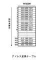
図6は、アドレス変換テーブルの説明図である。
このアドレス変換テーブルでは、1000ブロック分の論理ブロックアドレスに対応する物理ブロックが、物理通番で示されている。ここで、物理通番とは、各ゾーン内で物理ブロックアドレスの順番で付けた通番(2進数:000 0000 0000b〜011 1111 1111b)であり、各ゾーンに応じたオフセットを加えることにより、フラッシュメモリ2内での実際の物理ブロックアドレスに変換することができる。
FIG. 6 is an explanatory diagram of an address conversion table.
In this address conversion table, physical blocks corresponding to 1000 block logical block addresses are indicated by physical serial numbers. Here, the physical serial number is a serial number (binary number: 0000 0000 0000b to 011 1111 1111b) assigned in the order of the physical block address in each zone, and by adding an offset corresponding to each zone, the
例えば、フラッシュメモリ2内のブロックをアドレス順でゾーン0からゾーンNに割付けた場合、各ゾーンには次のようなオフセットが割当てられる。
ゾーン0:0
ゾーン1:0+1000×1
ゾーン2:0+1000×2
ゾーン3:0+1000×3
・
・
・
ゾーンN:0+1000×N
For example, when the blocks in the
Zone 0: 0
Zone 1: 0 + 1000x1
Zone 2: 0 + 1000x2
Zone 3: 0 + 1000x3
・
・
・
Zone N: 0 + 1000 × N
このアドレス変換テーブルを用いて論理ブロックアドレスを物理ブロックアドレスに変換するときは、ATAバス4を介して与えられる論理ブロックアドレスの割当てられているゾーン(ゾーン0〜Nのいずれかのゾーン)を求め、そのゾーンに対応するアドレス変換テーブルを用いてアドレス変換処理を行なう。
When a logical block address is converted into a physical block address using this address conversion table, a zone to which a logical block address given via the
このアドレス変換処理では、ATAバス4を介して与えられる論理ブロックアドレスから求めた論理通番に対応する物理通番をアドレス変換テーブルから読出し、読出した物理通番を物理ブロックアドレスに変換する。
In this address conversion process, the physical sequence number corresponding to the logical sequence number obtained from the logical block address given via the
例えば、図6の例では、ATAバス4を介して与えられた論理ブロックアドレスから求めた論理通番が“0”であれば、この論理通番に対応する物理通番は“9”(000 0000 1001b(2進数))になる。同様に、論理ブロックアドレスから求めた論理通番が“1”であれば、この論理通番に対応する物理通番は“2”(000 0000 0010b(2進数))になる。この物理通番に、各ゾーンに割当てられているオフセットを加えることにより、論理ブロックアドレスを物理ブロックアドレスに変換することができる。
For example, in the example of FIG. 6, if the logical sequence number obtained from the logical block address given via the
図6に示したアドレス変換テーブルを作成する場合、例えば、1000ブロック分の物理通番を記述できる領域をワークエリア8上に確保する。この際、1000ブロック分の領域を、論理通番の順番で、各論理通番に対応する物理通番を記述する領域として割当てる。ここで、更に、各論理通番に対応するデータが記憶されているか否かを判断するために、データが記憶されているか否かを示す情報を設定できるようにすることが好ましい。図6では、最上位ビットが“1”のとき、データが記憶されていないことを示している。
When the address conversion table shown in FIG. 6 is created, for example, an area where a physical serial number for 1000 blocks can be described is secured on the
例えば、特定のビットを、データが記憶されているか否かを示す情報に割当て、そのビットの論理値によってデータが記憶されているか否かを示すようにしてもよい。 For example, a specific bit may be assigned to information indicating whether or not data is stored, and whether or not data is stored is indicated by a logical value of the bit.
このデータが記憶されているか否かを示す情報は、テーブル作成開始時に、データが記憶されていないことを示す値に初期設定される。その後、アドレス変換テーブルを作成するゾーン内の各ブロックの冗長領域を順次読出していき、冗長領域に論理通番が記述されていた場合には、アドレス変換テーブルにおいてその論理通番に対応する部分に、その論理通番が記述されていたブロックの物理通番を記述し、更に、データが記憶されていないことを示す情報を、データが記憶されていることを示す値に変更する。この処理を、ゾーンを構成する1024の各ブロックについて順次行なっていき、この処理が完了するとアドレス変換テーブルが完成する。 Information indicating whether or not this data is stored is initially set to a value indicating that no data is stored at the start of table creation. After that, the redundant area of each block in the zone for creating the address conversion table is sequentially read, and when the logical serial number is described in the redundant area, the part corresponding to the logical serial number in the address conversion table is The physical serial number of the block in which the logical serial number is described is described, and information indicating that no data is stored is changed to a value indicating that data is stored. This process is sequentially performed for each of the 1024 blocks constituting the zone, and when this process is completed, the address conversion table is completed.
フラッシュメモリモジュール1におけるデータの書替処理では、ブロック消去されている消去済みブロックに新たなデータ(書替後のデータ)を書込み、その後、古いデータ(書替前のデータ)が書込まれていたブロックを消去する。この書替処理では、論理ブロックアドレスと物理ブロックアドレスの対応関係(論理通番と物理通番の対応関係)が、データの書替処理を行なう毎に変化するので、マイクロプロセッサ6は、アドレス変換テーブル上で対応関係が変化した部分をその都度、更新する。
In the data rewriting process in the
次に、消去済みブロックを検索するためのテーブルである消去済みブロック検索用テーブルについて説明する。 Next, an erased block search table that is a table for searching for erased blocks will be described.
図7(a),(b)は、消去済みブロック検索用テーブルの説明図である。
書替処理では、この消去済みブロック検索用テーブルで検索した消去済みブロックに、新たなデータ(書替後のデータ)が書込まれる。この消去済みブロック検索用テーブルは、ワークエリア8上に作成される。
7A and 7B are explanatory diagrams of the erased block search table.
In the rewriting process, new data (data after rewriting) is written in the erased block searched in the erased block search table. This erased block search table is created on the
消去済みブロック検索用テーブルでは、ゾーンを構成する各ブロックを、ワークエリア8を構成するSRAM上の各ビットに対応させ、各ビットの論理値の“0”又は“1”で、データが書込まれている状態、又はデータが書込まれていない状態をそれぞれ示している。
In the erased block search table, each block constituting the zone is associated with each bit on the SRAM constituting the
ゾーンを構成する各ブロックとSRAM上の各ビットとの対応関係については、消去済みブロック検索用テーブル上のビットを、若番側から順に(図7(a)のように上の行から下の行へ、各行を左から右へ)物理通番の順番に対応させている。従って、消去済みブロック検索用テーブルの左上のビットが、物理通番0のブロックに対応し、右下のビットが、物理通番1023のブロックに対応する。各ビットの論理値については、データが書込まれている場合(又は不良ブロックであることを示すブロックステータスが記述されている場合)は、そのビットに“0”を、データが書込まれていない場合(消去済みブロックの場合)は、そのビットに“1”を設定する。
Regarding the correspondence between each block constituting the zone and each bit on the SRAM, the bit on the erased block search table is changed in order from the younger number (from the upper row to the lower row as shown in FIG. 7A). (Each row from left to right) The physical sequence numbers correspond to each other. Accordingly, the upper left bit of the erased block search table corresponds to the block having the
この消去済みブロック検索用テーブルは、アドレス変換テーブルを作成する際に一緒に作成することができる。 The erased block search table can be created together with the address conversion table.
例えば、消去済みブロック検索用テーブルを作成するSRAM上の領域に"0"を設定しておき、各ブロックの冗長領域に対応論理ブロックアドレスも不良ブロックであることを示すブロックステータスも記述されていないときに、そのブロックに対応するビットに“1”を設定するようにすれば、アドレス変換テーブルを作成する際に一緒に作成することができる。 For example, “0” is set in the SRAM area for creating the erased block search table, and the corresponding logical block address is not described in the redundant area of each block and the block status indicating that it is a bad block is not described. Sometimes, if the bit corresponding to the block is set to “1”, the address conversion table can be created together.
又、この消去済みブロック検索用テーブルの更新については、消去済みブロックにデータを書込んだときに、そのブロックに対応するビットを“1”から“0”に変更し、データが書込まれているブロックをブロック消去したときに、そのブロックに対応するビットを“0"から“1”に変更する。 As for updating the erased block search table, when data is written to the erased block, the bit corresponding to the block is changed from “1” to “0” and the data is written. When a block is erased, the bit corresponding to that block is changed from “0” to “1”.
この消去済みブロック検索用テーブルを用いて、消去済みブロックを検索する場合、物理通番0に対応するビット(図7(b)の一番上の行の一番左のビット)から、物理通番1023に対応するビット(図7(b)の一番下の行の一番右のビット)までを走査していき、消去済みブロックに対応する“1”のビットを検索する。
When an erased block is searched using this erased block search table, the
その結果、例えば走査の途中でテーブルで消去済みブロックに対応する“1”のビットが検出された場合、そこで検索を終了し、そのビットに対応する物理通番のブロックが、新たなデータ(書替後のデータ)が書込まれる物理ブロックになる。次回の検索は、消去済みブロックとして検出された“1”のビットの次のビットから走査が開始される。その後も、同様の検索を続けていき、最期のブロックに相当するビットまで走査が進んだときは、最初のブロックに相当するビットに戻る。このようにして検索された消去済みブロックに、新たなデータ(書替後のデータ)が書込まれる。 As a result, for example, when a bit of “1” corresponding to the erased block is detected in the table in the middle of scanning, the search is terminated, and the block having the physical serial number corresponding to the bit is replaced with new data (rewrite). It becomes a physical block to be written. The next search starts scanning from the bit next to the “1” bit detected as an erased block. Thereafter, the same search is continued, and when the scan advances to the bit corresponding to the last block, the bit returns to the bit corresponding to the first block. New data (data after rewriting) is written in the erased block searched in this way.
以上のように、本発明の実施形態に係るフラッシュメモリモジュール1は、ホストシステムのATAバス4に電気的に接続されるコネクタ14aと、フラッシュメモリ2と、メモリコントローラ3とを、基板15に搭載したので、ホストシステムの内部に実施可能になっている。
As described above, the
また、基板15の一方の面にフラッシュメモリ2が実装され、他方の面にメモリコントローラ3が搭載されているので、基板15の面積を小さくすることができる。
Further, since the
また、主基板16側から供給される電源の電圧が所定の電圧レベルに達するまで、フラッシュメモリ2及びメモリコントローラ3が起動しないように制御する回路を基板15に設けることにより、フラッシュメモリモジュール1の誤動作を防止できる。
また、コネクタ14aによって、ホストシステムが接続されるので、不具合が生じたときにも交換が可能である。
Further, by providing a circuit on the
Further, since the host system is connected by the
1 フラッシュメモリモジュール
2 フラッシュメモリ
3 メモリコントローラ
4 ATAバス
5 ホストインターフェース制御ブロック
6 マイクロプロセッサ
7 ホストインターフェースブロック
8 ワークエリア
9 バッファ
10 内部インターフェースブロック
11 ECCブロック
12 フラッシュメモリシーケンサブロック
13 内部バス
14a コネクタ
15 基板
16 主基板
DESCRIPTION OF
Claims (4)
フラッシュメモリと、
前記フラッシュメモリに接続され、前記コネクタを介して前記バスから与えられる書込み命令若しくは読出し命令に基づいて該フラッシュメモリに対するアクセスを制御する制御回路と、
前記コネクタ、前記制御回路及び前記フラッシュメモリが実装された基板と、
を備えることを特徴とするフラッシュメモリモジュール。 A connector electrically connected to the bus of the host system;
Flash memory,
A control circuit connected to the flash memory and controlling access to the flash memory based on a write command or a read command given from the bus via the connector;
A board on which the connector, the control circuit and the flash memory are mounted;
A flash memory module comprising:
前記電圧値が予め設定された電圧値に達するまで、前記制御回路を停止状態にする起動制御回路と、
を備えることを特徴とする請求項1に記載のフラッシュメモリモジュール。 Means for detecting a voltage value of a power source supplied via the connector;
A start control circuit that stops the control circuit until the voltage value reaches a preset voltage value;
The flash memory module according to claim 1, comprising:
4. The flash memory module according to claim 1, wherein at least a part of the control circuit and the flash memory are mounted on different surfaces of the substrate. 5.
Priority Applications (1)
| Application Number | Priority Date | Filing Date | Title |
|---|---|---|---|
| JP2004222375A JP2006040484A (en) | 2004-07-29 | 2004-07-29 | Flash memory module |
Applications Claiming Priority (1)
| Application Number | Priority Date | Filing Date | Title |
|---|---|---|---|
| JP2004222375A JP2006040484A (en) | 2004-07-29 | 2004-07-29 | Flash memory module |
Publications (1)
| Publication Number | Publication Date |
|---|---|
| JP2006040484A true JP2006040484A (en) | 2006-02-09 |
Family
ID=35905292
Family Applications (1)
| Application Number | Title | Priority Date | Filing Date |
|---|---|---|---|
| JP2004222375A Withdrawn JP2006040484A (en) | 2004-07-29 | 2004-07-29 | Flash memory module |
Country Status (1)
| Country | Link |
|---|---|
| JP (1) | JP2006040484A (en) |
Cited By (2)
| Publication number | Priority date | Publication date | Assignee | Title |
|---|---|---|---|---|
| US7870328B2 (en) | 2006-04-17 | 2011-01-11 | Tdk Corporation | Memory controller and flash memory system |
| JP2013206453A (en) * | 2012-03-29 | 2013-10-07 | Innodisk Corp | Motherboard and embedded memory module inserted thereinto |
-
2004
- 2004-07-29 JP JP2004222375A patent/JP2006040484A/en not_active Withdrawn
Cited By (2)
| Publication number | Priority date | Publication date | Assignee | Title |
|---|---|---|---|---|
| US7870328B2 (en) | 2006-04-17 | 2011-01-11 | Tdk Corporation | Memory controller and flash memory system |
| JP2013206453A (en) * | 2012-03-29 | 2013-10-07 | Innodisk Corp | Motherboard and embedded memory module inserted thereinto |
Similar Documents
| Publication | Publication Date | Title |
|---|---|---|
| US7944748B2 (en) | Erase block data splitting | |
| US7330995B2 (en) | Nonvolatile memory apparatus which prevents destruction of write data caused by power shutdown during a writing process | |
| US7254060B2 (en) | Nonvolatile semiconductor memory device | |
| US7315870B2 (en) | Memory controller, flash memory system, and method for recording data on flash memory | |
| JP4245585B2 (en) | Memory controller, flash memory system, and flash memory control method | |
| JP2006018373A (en) | Memory controller, flash memory system and control method for flash memory | |
| JP4373943B2 (en) | Memory controller, flash memory system, and flash memory control method | |
| CN115701638A (en) | Memory system and method of operation thereof | |
| JP4177360B2 (en) | Memory controller, flash memory system, and flash memory control method | |
| JP4433792B2 (en) | MEMORY CONTROLLER, FLASH MEMORY SYSTEM PROVIDED WITH MEMORY CONTROLLER, AND FLASH MEMORY CONTROL METHOD | |
| JP4177292B2 (en) | MEMORY CONTROLLER, FLASH MEMORY SYSTEM, AND FLASH MEMORY CONTROL METHOD | |
| JP2005316793A (en) | Flash memory system and flash memory control method | |
| JP2006040484A (en) | Flash memory module | |
| JP4641034B2 (en) | Nonvolatile storage system | |
| JP2005292925A (en) | Memory controller, flash memory system, and control method for flash memory | |
| JP4177301B2 (en) | Memory controller, flash memory system, and flash memory control method | |
| JP4194518B2 (en) | Memory controller, flash memory system, and flash memory control method | |
| JP4332108B2 (en) | Memory controller, flash memory system, and flash memory control method | |
| JP4419525B2 (en) | MEMORY CONTROLLER, FLASH MEMORY SYSTEM PROVIDED WITH MEMORY CONTROLLER, AND FLASH MEMORY CONTROL METHOD | |
| JP2005293177A (en) | Memory controller and flash memory system | |
| JP4304167B2 (en) | Memory controller, flash memory system, and flash memory control method | |
| JP2006099696A (en) | Memory controller, flash memory system provided with memory controller, and flash memory control method | |
| JP4245594B2 (en) | Memory controller and flash memory system | |
| JP2011048852A (en) | Nonvolatile memory system | |
| JP2006099594A (en) | Memory controller, flash memory system, and control method for flash memory |
Legal Events
| Date | Code | Title | Description |
|---|---|---|---|
| A300 | Withdrawal of application because of no request for examination |
Free format text: JAPANESE INTERMEDIATE CODE: A300 Effective date: 20071002 |