JP2005537496A - Resonance sensor and sensing system - Google Patents
Resonance sensor and sensing system Download PDFInfo
- Publication number
- JP2005537496A JP2005537496A JP2004546714A JP2004546714A JP2005537496A JP 2005537496 A JP2005537496 A JP 2005537496A JP 2004546714 A JP2004546714 A JP 2004546714A JP 2004546714 A JP2004546714 A JP 2004546714A JP 2005537496 A JP2005537496 A JP 2005537496A
- Authority
- JP
- Japan
- Prior art keywords
- movable member
- substrate
- sensor
- receptor
- measurement object
- Prior art date
- Legal status (The legal status is an assumption and is not a legal conclusion. Google has not performed a legal analysis and makes no representation as to the accuracy of the status listed.)
- Pending
Links
- 239000000758 substrate Substances 0.000 claims abstract description 104
- 238000005259 measurement Methods 0.000 claims abstract description 92
- 230000033001 locomotion Effects 0.000 claims abstract description 49
- 238000000034 method Methods 0.000 claims description 86
- 230000003287 optical effect Effects 0.000 claims description 49
- 229910052751 metal Inorganic materials 0.000 claims description 35
- 239000002184 metal Substances 0.000 claims description 35
- 239000010703 silicon Substances 0.000 claims description 28
- 229910052710 silicon Inorganic materials 0.000 claims description 27
- 230000010355 oscillation Effects 0.000 claims description 24
- 238000012544 monitoring process Methods 0.000 claims description 21
- PCHJSUWPFVWCPO-UHFFFAOYSA-N gold Chemical compound [Au] PCHJSUWPFVWCPO-UHFFFAOYSA-N 0.000 claims description 15
- 229910052737 gold Inorganic materials 0.000 claims description 15
- 239000010931 gold Substances 0.000 claims description 15
- 230000004044 response Effects 0.000 claims description 7
- XEEYBQQBJWHFJM-UHFFFAOYSA-N Iron Chemical compound [Fe] XEEYBQQBJWHFJM-UHFFFAOYSA-N 0.000 claims description 6
- PXHVJJICTQNCMI-UHFFFAOYSA-N Nickel Chemical compound [Ni] PXHVJJICTQNCMI-UHFFFAOYSA-N 0.000 claims description 6
- RYGMFSIKBFXOCR-UHFFFAOYSA-N Copper Chemical compound [Cu] RYGMFSIKBFXOCR-UHFFFAOYSA-N 0.000 claims description 5
- 229910052802 copper Inorganic materials 0.000 claims description 5
- 239000010949 copper Substances 0.000 claims description 5
- 229910052742 iron Inorganic materials 0.000 claims description 3
- 229910052759 nickel Inorganic materials 0.000 claims description 3
- 102000005962 receptors Human genes 0.000 description 104
- 108020003175 receptors Proteins 0.000 description 104
- 239000000523 sample Substances 0.000 description 79
- 239000010410 layer Substances 0.000 description 73
- 230000008569 process Effects 0.000 description 45
- 230000000903 blocking effect Effects 0.000 description 41
- 230000027455 binding Effects 0.000 description 34
- XUIMIQQOPSSXEZ-UHFFFAOYSA-N Silicon Chemical compound [Si] XUIMIQQOPSSXEZ-UHFFFAOYSA-N 0.000 description 29
- 239000000463 material Substances 0.000 description 28
- 239000000126 substance Substances 0.000 description 28
- 239000013545 self-assembled monolayer Substances 0.000 description 24
- 235000012431 wafers Nutrition 0.000 description 22
- 230000008859 change Effects 0.000 description 21
- 238000005530 etching Methods 0.000 description 19
- 108091033319 polynucleotide Proteins 0.000 description 19
- 102000040430 polynucleotide Human genes 0.000 description 19
- 239000002157 polynucleotide Substances 0.000 description 19
- 229920002120 photoresistant polymer Polymers 0.000 description 17
- 229920000642 polymer Polymers 0.000 description 16
- 239000007788 liquid Substances 0.000 description 15
- 230000000694 effects Effects 0.000 description 14
- 238000012545 processing Methods 0.000 description 14
- VYPSYNLAJGMNEJ-UHFFFAOYSA-N Silicium dioxide Chemical compound O=[Si]=O VYPSYNLAJGMNEJ-UHFFFAOYSA-N 0.000 description 13
- 108090000623 proteins and genes Proteins 0.000 description 13
- -1 such as a vapor Substances 0.000 description 13
- 102000004169 proteins and genes Human genes 0.000 description 12
- 239000003921 oil Substances 0.000 description 10
- 239000011521 glass Substances 0.000 description 9
- 239000012530 fluid Substances 0.000 description 8
- 238000004519 manufacturing process Methods 0.000 description 8
- 239000002777 nucleoside Substances 0.000 description 8
- 210000004027 cell Anatomy 0.000 description 7
- 230000006870 function Effects 0.000 description 7
- 239000003607 modifier Substances 0.000 description 7
- 102000039446 nucleic acids Human genes 0.000 description 7
- 108020004707 nucleic acids Proteins 0.000 description 7
- 150000007523 nucleic acids Chemical class 0.000 description 7
- 150000003833 nucleoside derivatives Chemical class 0.000 description 7
- LMDZBCPBFSXMTL-UHFFFAOYSA-N 1-ethyl-3-(3-dimethylaminopropyl)carbodiimide Chemical compound CCN=C=NCCCN(C)C LMDZBCPBFSXMTL-UHFFFAOYSA-N 0.000 description 6
- 108091023037 Aptamer Proteins 0.000 description 6
- 239000012491 analyte Substances 0.000 description 6
- 238000000576 coating method Methods 0.000 description 6
- 150000001875 compounds Chemical class 0.000 description 6
- 238000001514 detection method Methods 0.000 description 6
- 238000006073 displacement reaction Methods 0.000 description 6
- 239000000377 silicon dioxide Substances 0.000 description 6
- 235000012239 silicon dioxide Nutrition 0.000 description 6
- 239000000243 solution Substances 0.000 description 6
- 239000013626 chemical specie Substances 0.000 description 5
- 238000000151 deposition Methods 0.000 description 5
- 238000010586 diagram Methods 0.000 description 5
- 230000007613 environmental effect Effects 0.000 description 5
- 229940088597 hormone Drugs 0.000 description 5
- 239000005556 hormone Substances 0.000 description 5
- 239000003446 ligand Substances 0.000 description 5
- 230000001105 regulatory effect Effects 0.000 description 5
- RWQNBRDOKXIBIV-UHFFFAOYSA-N thymine Chemical compound CC1=CNC(=O)NC1=O RWQNBRDOKXIBIV-UHFFFAOYSA-N 0.000 description 5
- UHDGCWIWMRVCDJ-UHFFFAOYSA-N 1-beta-D-Xylofuranosyl-NH-Cytosine Natural products O=C1N=C(N)C=CN1C1C(O)C(O)C(CO)O1 UHDGCWIWMRVCDJ-UHFFFAOYSA-N 0.000 description 4
- FZWGECJQACGGTI-UHFFFAOYSA-N 2-amino-7-methyl-1,7-dihydro-6H-purin-6-one Chemical compound NC1=NC(O)=C2N(C)C=NC2=N1 FZWGECJQACGGTI-UHFFFAOYSA-N 0.000 description 4
- OVONXEQGWXGFJD-UHFFFAOYSA-N 4-sulfanylidene-1h-pyrimidin-2-one Chemical compound SC=1C=CNC(=O)N=1 OVONXEQGWXGFJD-UHFFFAOYSA-N 0.000 description 4
- ZLAQATDNGLKIEV-UHFFFAOYSA-N 5-methyl-2-sulfanylidene-1h-pyrimidin-4-one Chemical compound CC1=CNC(=S)NC1=O ZLAQATDNGLKIEV-UHFFFAOYSA-N 0.000 description 4
- UHDGCWIWMRVCDJ-PSQAKQOGSA-N Cytidine Natural products O=C1N=C(N)C=CN1[C@@H]1[C@@H](O)[C@@H](O)[C@H](CO)O1 UHDGCWIWMRVCDJ-PSQAKQOGSA-N 0.000 description 4
- KRHYYFGTRYWZRS-UHFFFAOYSA-N Fluorane Chemical compound F KRHYYFGTRYWZRS-UHFFFAOYSA-N 0.000 description 4
- 229920002683 Glycosaminoglycan Polymers 0.000 description 4
- KDLHZDBZIXYQEI-UHFFFAOYSA-N Palladium Chemical compound [Pd] KDLHZDBZIXYQEI-UHFFFAOYSA-N 0.000 description 4
- 239000002202 Polyethylene glycol Substances 0.000 description 4
- ISAKRJDGNUQOIC-UHFFFAOYSA-N Uracil Chemical compound O=C1C=CNC(=O)N1 ISAKRJDGNUQOIC-UHFFFAOYSA-N 0.000 description 4
- 125000000217 alkyl group Chemical group 0.000 description 4
- 229910052782 aluminium Inorganic materials 0.000 description 4
- XAGFODPZIPBFFR-UHFFFAOYSA-N aluminium Chemical compound [Al] XAGFODPZIPBFFR-UHFFFAOYSA-N 0.000 description 4
- 238000006243 chemical reaction Methods 0.000 description 4
- 239000011248 coating agent Substances 0.000 description 4
- UHDGCWIWMRVCDJ-ZAKLUEHWSA-N cytidine Chemical compound O=C1N=C(N)C=CN1[C@H]1[C@H](O)[C@@H](O)[C@H](CO)O1 UHDGCWIWMRVCDJ-ZAKLUEHWSA-N 0.000 description 4
- 238000013461 design Methods 0.000 description 4
- LOKCTEFSRHRXRJ-UHFFFAOYSA-I dipotassium trisodium dihydrogen phosphate hydrogen phosphate dichloride Chemical compound P(=O)(O)(O)[O-].[K+].P(=O)(O)([O-])[O-].[Na+].[Na+].[Cl-].[K+].[Cl-].[Na+] LOKCTEFSRHRXRJ-UHFFFAOYSA-I 0.000 description 4
- 239000007789 gas Substances 0.000 description 4
- 230000003993 interaction Effects 0.000 description 4
- 230000002452 interceptive effect Effects 0.000 description 4
- 229910044991 metal oxide Inorganic materials 0.000 description 4
- 150000004706 metal oxides Chemical class 0.000 description 4
- 150000002739 metals Chemical class 0.000 description 4
- 230000004048 modification Effects 0.000 description 4
- 238000012986 modification Methods 0.000 description 4
- 239000002953 phosphate buffered saline Substances 0.000 description 4
- BASFCYQUMIYNBI-UHFFFAOYSA-N platinum Chemical compound [Pt] BASFCYQUMIYNBI-UHFFFAOYSA-N 0.000 description 4
- 229920001223 polyethylene glycol Polymers 0.000 description 4
- 150000003141 primary amines Chemical class 0.000 description 4
- 239000000047 product Substances 0.000 description 4
- 239000002904 solvent Substances 0.000 description 4
- 125000006850 spacer group Chemical group 0.000 description 4
- 238000006467 substitution reaction Methods 0.000 description 4
- 150000003573 thiols Chemical class 0.000 description 4
- 238000013519 translation Methods 0.000 description 4
- 125000006374 C2-C10 alkenyl group Chemical group 0.000 description 3
- 108020004414 DNA Proteins 0.000 description 3
- 241000233866 Fungi Species 0.000 description 3
- 240000004808 Saccharomyces cerevisiae Species 0.000 description 3
- RTAQQCXQSZGOHL-UHFFFAOYSA-N Titanium Chemical compound [Ti] RTAQQCXQSZGOHL-UHFFFAOYSA-N 0.000 description 3
- 241000700605 Viruses Species 0.000 description 3
- 125000000304 alkynyl group Chemical group 0.000 description 3
- 230000000295 complement effect Effects 0.000 description 3
- 230000021615 conjugation Effects 0.000 description 3
- 230000001276 controlling effect Effects 0.000 description 3
- 239000013067 intermediate product Substances 0.000 description 3
- 238000005304 joining Methods 0.000 description 3
- 239000011133 lead Substances 0.000 description 3
- 230000000670 limiting effect Effects 0.000 description 3
- 244000052769 pathogen Species 0.000 description 3
- 230000001717 pathogenic effect Effects 0.000 description 3
- 238000001020 plasma etching Methods 0.000 description 3
- 238000007747 plating Methods 0.000 description 3
- 238000012552 review Methods 0.000 description 3
- 150000003384 small molecules Chemical class 0.000 description 3
- 230000003068 static effect Effects 0.000 description 3
- 235000000346 sugar Nutrition 0.000 description 3
- 238000012360 testing method Methods 0.000 description 3
- 239000010936 titanium Substances 0.000 description 3
- 229910052719 titanium Inorganic materials 0.000 description 3
- YBJHBAHKTGYVGT-ZKWXMUAHSA-N (+)-Biotin Chemical compound N1C(=O)N[C@@H]2[C@H](CCCCC(=O)O)SC[C@@H]21 YBJHBAHKTGYVGT-ZKWXMUAHSA-N 0.000 description 2
- RFLVMTUMFYRZCB-UHFFFAOYSA-N 1-methylguanine Chemical compound O=C1N(C)C(N)=NC2=C1N=CN2 RFLVMTUMFYRZCB-UHFFFAOYSA-N 0.000 description 2
- OIVLITBTBDPEFK-UHFFFAOYSA-N 5,6-dihydrouracil Chemical compound O=C1CCNC(=O)N1 OIVLITBTBDPEFK-UHFFFAOYSA-N 0.000 description 2
- RYVNIFSIEDRLSJ-UHFFFAOYSA-N 5-(hydroxymethyl)cytosine Chemical compound NC=1NC(=O)N=CC=1CO RYVNIFSIEDRLSJ-UHFFFAOYSA-N 0.000 description 2
- GSPMCUUYNASDHM-UHFFFAOYSA-N 5-methyl-4-sulfanylidene-1h-pyrimidin-2-one Chemical compound CC1=CNC(=O)N=C1S GSPMCUUYNASDHM-UHFFFAOYSA-N 0.000 description 2
- CKOMXBHMKXXTNW-UHFFFAOYSA-N 6-methyladenine Chemical compound CNC1=NC=NC2=C1N=CN2 CKOMXBHMKXXTNW-UHFFFAOYSA-N 0.000 description 2
- PEHVGBZKEYRQSX-UHFFFAOYSA-N 7-deaza-adenine Chemical compound NC1=NC=NC2=C1C=CN2 PEHVGBZKEYRQSX-UHFFFAOYSA-N 0.000 description 2
- HCGHYQLFMPXSDU-UHFFFAOYSA-N 7-methyladenine Chemical compound C1=NC(N)=C2N(C)C=NC2=N1 HCGHYQLFMPXSDU-UHFFFAOYSA-N 0.000 description 2
- KDCGOANMDULRCW-UHFFFAOYSA-N 7H-purine Chemical compound N1=CNC2=NC=NC2=C1 KDCGOANMDULRCW-UHFFFAOYSA-N 0.000 description 2
- UJOBWOGCFQCDNV-UHFFFAOYSA-N 9H-carbazole Chemical compound C1=CC=C2C3=CC=CC=C3NC2=C1 UJOBWOGCFQCDNV-UHFFFAOYSA-N 0.000 description 2
- RZVAJINKPMORJF-UHFFFAOYSA-N Acetaminophen Chemical compound CC(=O)NC1=CC=C(O)C=C1 RZVAJINKPMORJF-UHFFFAOYSA-N 0.000 description 2
- 108060003345 Adrenergic Receptor Proteins 0.000 description 2
- 102000017910 Adrenergic receptor Human genes 0.000 description 2
- JBRZTFJDHDCESZ-UHFFFAOYSA-N AsGa Chemical compound [As]#[Ga] JBRZTFJDHDCESZ-UHFFFAOYSA-N 0.000 description 2
- 241000894006 Bacteria Species 0.000 description 2
- ZOXJGFHDIHLPTG-UHFFFAOYSA-N Boron Chemical compound [B] ZOXJGFHDIHLPTG-UHFFFAOYSA-N 0.000 description 2
- VYZAMTAEIAYCRO-UHFFFAOYSA-N Chromium Chemical compound [Cr] VYZAMTAEIAYCRO-UHFFFAOYSA-N 0.000 description 2
- 108090000695 Cytokines Proteins 0.000 description 2
- 102000004127 Cytokines Human genes 0.000 description 2
- FBPFZTCFMRRESA-KVTDHHQDSA-N D-Mannitol Chemical compound OC[C@@H](O)[C@@H](O)[C@H](O)[C@H](O)CO FBPFZTCFMRRESA-KVTDHHQDSA-N 0.000 description 2
- 125000000824 D-ribofuranosyl group Chemical group [H]OC([H])([H])[C@@]1([H])OC([H])(*)[C@]([H])(O[H])[C@]1([H])O[H] 0.000 description 2
- 229910001218 Gallium arsenide Inorganic materials 0.000 description 2
- 108090000288 Glycoproteins Proteins 0.000 description 2
- 102000003886 Glycoproteins Human genes 0.000 description 2
- 102000017727 Immunoglobulin Variable Region Human genes 0.000 description 2
- 108010067060 Immunoglobulin Variable Region Proteins 0.000 description 2
- 229930195725 Mannitol Natural products 0.000 description 2
- HYVABZIGRDEKCD-UHFFFAOYSA-N N(6)-dimethylallyladenine Chemical compound CC(C)=CCNC1=NC=NC2=C1N=CN2 HYVABZIGRDEKCD-UHFFFAOYSA-N 0.000 description 2
- 102000007399 Nuclear hormone receptor Human genes 0.000 description 2
- 108091093037 Peptide nucleic acid Proteins 0.000 description 2
- 102000029797 Prion Human genes 0.000 description 2
- 108091000054 Prion Proteins 0.000 description 2
- BQCADISMDOOEFD-UHFFFAOYSA-N Silver Chemical compound [Ag] BQCADISMDOOEFD-UHFFFAOYSA-N 0.000 description 2
- 108010090804 Streptavidin Proteins 0.000 description 2
- 239000002250 absorbent Substances 0.000 description 2
- 230000002745 absorbent Effects 0.000 description 2
- 239000002253 acid Substances 0.000 description 2
- 125000003277 amino group Chemical group 0.000 description 2
- 239000000427 antigen Substances 0.000 description 2
- 108091007433 antigens Proteins 0.000 description 2
- 102000036639 antigens Human genes 0.000 description 2
- 230000008901 benefit Effects 0.000 description 2
- 229910052796 boron Inorganic materials 0.000 description 2
- 239000000872 buffer Substances 0.000 description 2
- 150000001720 carbohydrates Chemical class 0.000 description 2
- 235000014633 carbohydrates Nutrition 0.000 description 2
- 125000003178 carboxy group Chemical group [H]OC(*)=O 0.000 description 2
- HVYWMOMLDIMFJA-DPAQBDIFSA-N cholesterol Chemical compound C1C=C2C[C@@H](O)CC[C@]2(C)[C@@H]2[C@@H]1[C@@H]1CC[C@H]([C@H](C)CCCC(C)C)[C@@]1(C)CC2 HVYWMOMLDIMFJA-DPAQBDIFSA-N 0.000 description 2
- 229910052804 chromium Inorganic materials 0.000 description 2
- 239000011651 chromium Substances 0.000 description 2
- 238000005260 corrosion Methods 0.000 description 2
- 230000007797 corrosion Effects 0.000 description 2
- 108091007930 cytoplasmic receptors Proteins 0.000 description 2
- 238000000354 decomposition reaction Methods 0.000 description 2
- 230000008021 deposition Effects 0.000 description 2
- 235000014113 dietary fatty acids Nutrition 0.000 description 2
- VYFYYTLLBUKUHU-UHFFFAOYSA-N dopamine Chemical compound NCCC1=CC=C(O)C(O)=C1 VYFYYTLLBUKUHU-UHFFFAOYSA-N 0.000 description 2
- 238000009713 electroplating Methods 0.000 description 2
- 239000002360 explosive Substances 0.000 description 2
- 229930195729 fatty acid Natural products 0.000 description 2
- 239000000194 fatty acid Substances 0.000 description 2
- 150000004665 fatty acids Chemical class 0.000 description 2
- 150000004676 glycans Chemical class 0.000 description 2
- 239000003102 growth factor Substances 0.000 description 2
- 229930195733 hydrocarbon Natural products 0.000 description 2
- 125000002887 hydroxy group Chemical group [H]O* 0.000 description 2
- 230000036039 immunity Effects 0.000 description 2
- 238000007373 indentation Methods 0.000 description 2
- NOESYZHRGYRDHS-UHFFFAOYSA-N insulin Chemical compound N1C(=O)C(NC(=O)C(CCC(N)=O)NC(=O)C(CCC(O)=O)NC(=O)C(C(C)C)NC(=O)C(NC(=O)CN)C(C)CC)CSSCC(C(NC(CO)C(=O)NC(CC(C)C)C(=O)NC(CC=2C=CC(O)=CC=2)C(=O)NC(CCC(N)=O)C(=O)NC(CC(C)C)C(=O)NC(CCC(O)=O)C(=O)NC(CC(N)=O)C(=O)NC(CC=2C=CC(O)=CC=2)C(=O)NC(CSSCC(NC(=O)C(C(C)C)NC(=O)C(CC(C)C)NC(=O)C(CC=2C=CC(O)=CC=2)NC(=O)C(CC(C)C)NC(=O)C(C)NC(=O)C(CCC(O)=O)NC(=O)C(C(C)C)NC(=O)C(CC(C)C)NC(=O)C(CC=2NC=NC=2)NC(=O)C(CO)NC(=O)CNC2=O)C(=O)NCC(=O)NC(CCC(O)=O)C(=O)NC(CCCNC(N)=N)C(=O)NCC(=O)NC(CC=3C=CC=CC=3)C(=O)NC(CC=3C=CC=CC=3)C(=O)NC(CC=3C=CC(O)=CC=3)C(=O)NC(C(C)O)C(=O)N3C(CCC3)C(=O)NC(CCCCN)C(=O)NC(C)C(O)=O)C(=O)NC(CC(N)=O)C(O)=O)=O)NC(=O)C(C(C)CC)NC(=O)C(CO)NC(=O)C(C(C)O)NC(=O)C1CSSCC2NC(=O)C(CC(C)C)NC(=O)C(NC(=O)C(CCC(N)=O)NC(=O)C(CC(N)=O)NC(=O)C(NC(=O)C(N)CC=1C=CC=CC=1)C(C)C)CC1=CN=CN1 NOESYZHRGYRDHS-UHFFFAOYSA-N 0.000 description 2
- 239000000594 mannitol Substances 0.000 description 2
- 235000010355 mannitol Nutrition 0.000 description 2
- 230000009871 nonspecific binding Effects 0.000 description 2
- 125000003835 nucleoside group Chemical group 0.000 description 2
- 239000002773 nucleotide Substances 0.000 description 2
- 125000003729 nucleotide group Chemical group 0.000 description 2
- 229910052763 palladium Inorganic materials 0.000 description 2
- 239000002245 particle Substances 0.000 description 2
- 238000000059 patterning Methods 0.000 description 2
- 238000000206 photolithography Methods 0.000 description 2
- 230000010399 physical interaction Effects 0.000 description 2
- 229910052697 platinum Inorganic materials 0.000 description 2
- 102000054765 polymorphisms of proteins Human genes 0.000 description 2
- 229920001282 polysaccharide Polymers 0.000 description 2
- 239000005017 polysaccharide Substances 0.000 description 2
- 238000007639 printing Methods 0.000 description 2
- 238000003672 processing method Methods 0.000 description 2
- 239000005297 pyrex Substances 0.000 description 2
- 230000005855 radiation Effects 0.000 description 2
- 238000000926 separation method Methods 0.000 description 2
- 229910052709 silver Inorganic materials 0.000 description 2
- 239000004332 silver Substances 0.000 description 2
- 150000008163 sugars Chemical class 0.000 description 2
- 229940035893 uracil Drugs 0.000 description 2
- HDTRYLNUVZCQOY-UHFFFAOYSA-N α-D-glucopyranosyl-α-D-glucopyranoside Natural products OC1C(O)C(O)C(CO)OC1OC1C(O)C(O)C(O)C(CO)O1 HDTRYLNUVZCQOY-UHFFFAOYSA-N 0.000 description 1
- UCTWMZQNUQWSLP-VIFPVBQESA-N (R)-adrenaline Chemical compound CNC[C@H](O)C1=CC=C(O)C(O)=C1 UCTWMZQNUQWSLP-VIFPVBQESA-N 0.000 description 1
- 229930182837 (R)-adrenaline Natural products 0.000 description 1
- WJFKNYWRSNBZNX-UHFFFAOYSA-N 10H-phenothiazine Chemical compound C1=CC=C2NC3=CC=CC=C3SC2=C1 WJFKNYWRSNBZNX-UHFFFAOYSA-N 0.000 description 1
- TZMSYXZUNZXBOL-UHFFFAOYSA-N 10H-phenoxazine Chemical compound C1=CC=C2NC3=CC=CC=C3OC2=C1 TZMSYXZUNZXBOL-UHFFFAOYSA-N 0.000 description 1
- WYDKPTZGVLTYPG-UHFFFAOYSA-N 2,8-diamino-3,7-dihydropurin-6-one Chemical compound N1C(N)=NC(=O)C2=C1N=C(N)N2 WYDKPTZGVLTYPG-UHFFFAOYSA-N 0.000 description 1
- HLYBTPMYFWWNJN-UHFFFAOYSA-N 2-(2,4-dioxo-1h-pyrimidin-5-yl)-2-hydroxyacetic acid Chemical compound OC(=O)C(O)C1=CNC(=O)NC1=O HLYBTPMYFWWNJN-UHFFFAOYSA-N 0.000 description 1
- SGAKLDIYNFXTCK-UHFFFAOYSA-N 2-[(2,4-dioxo-1h-pyrimidin-5-yl)methylamino]acetic acid Chemical compound OC(=O)CNCC1=CNC(=O)NC1=O SGAKLDIYNFXTCK-UHFFFAOYSA-N 0.000 description 1
- YSAJFXWTVFGPAX-UHFFFAOYSA-N 2-[(2,4-dioxo-1h-pyrimidin-5-yl)oxy]acetic acid Chemical compound OC(=O)COC1=CNC(=O)NC1=O YSAJFXWTVFGPAX-UHFFFAOYSA-N 0.000 description 1
- SVBOROZXXYRWJL-UHFFFAOYSA-N 2-[(4-oxo-2-sulfanylidene-1h-pyrimidin-5-yl)methylamino]acetic acid Chemical compound OC(=O)CNCC1=CNC(=S)NC1=O SVBOROZXXYRWJL-UHFFFAOYSA-N 0.000 description 1
- HTOVHZGIBCAAJU-UHFFFAOYSA-N 2-amino-2-propyl-1h-purin-6-one Chemical compound CCCC1(N)NC(=O)C2=NC=NC2=N1 HTOVHZGIBCAAJU-UHFFFAOYSA-N 0.000 description 1
- XQCZBXHVTFVIFE-UHFFFAOYSA-N 2-amino-4-hydroxypyrimidine Chemical compound NC1=NC=CC(O)=N1 XQCZBXHVTFVIFE-UHFFFAOYSA-N 0.000 description 1
- JHEKNTQSGTVPAO-UHFFFAOYSA-N 2-amino-8-sulfanylidene-7,9-dihydro-3h-purin-6-one Chemical compound N1C(N)=NC(=O)C2=C1NC(=S)N2 JHEKNTQSGTVPAO-UHFFFAOYSA-N 0.000 description 1
- XMSMHKMPBNTBOD-UHFFFAOYSA-N 2-dimethylamino-6-hydroxypurine Chemical compound N1C(N(C)C)=NC(=O)C2=C1N=CN2 XMSMHKMPBNTBOD-UHFFFAOYSA-N 0.000 description 1
- NEAQRZUHTPSBBM-UHFFFAOYSA-N 2-hydroxy-3,3-dimethyl-7-nitro-4h-isoquinolin-1-one Chemical compound C1=C([N+]([O-])=O)C=C2C(=O)N(O)C(C)(C)CC2=C1 NEAQRZUHTPSBBM-UHFFFAOYSA-N 0.000 description 1
- 125000003903 2-propenyl group Chemical group [H]C([*])([H])C([H])=C([H])[H] 0.000 description 1
- KOLPWZCZXAMXKS-UHFFFAOYSA-N 3-methylcytosine Chemical compound CN1C(N)=CC=NC1=O KOLPWZCZXAMXKS-UHFFFAOYSA-N 0.000 description 1
- GJAKJCICANKRFD-UHFFFAOYSA-N 4-acetyl-4-amino-1,3-dihydropyrimidin-2-one Chemical compound CC(=O)C1(N)NC(=O)NC=C1 GJAKJCICANKRFD-UHFFFAOYSA-N 0.000 description 1
- RTNUTCOTGVKVBR-UHFFFAOYSA-N 4-chlorotriazine Chemical class ClC1=CC=NN=N1 RTNUTCOTGVKVBR-UHFFFAOYSA-N 0.000 description 1
- NBAKTGXDIBVZOO-UHFFFAOYSA-N 5,6-dihydrothymine Chemical compound CC1CNC(=O)NC1=O NBAKTGXDIBVZOO-UHFFFAOYSA-N 0.000 description 1
- MQJSSLBGAQJNER-UHFFFAOYSA-N 5-(methylaminomethyl)-1h-pyrimidine-2,4-dione Chemical compound CNCC1=CNC(=O)NC1=O MQJSSLBGAQJNER-UHFFFAOYSA-N 0.000 description 1
- WPYRHVXCOQLYLY-UHFFFAOYSA-N 5-[(methoxyamino)methyl]-2-sulfanylidene-1h-pyrimidin-4-one Chemical compound CONCC1=CNC(=S)NC1=O WPYRHVXCOQLYLY-UHFFFAOYSA-N 0.000 description 1
- KELXHQACBIUYSE-UHFFFAOYSA-N 5-methoxy-1h-pyrimidine-2,4-dione Chemical compound COC1=CNC(=O)NC1=O KELXHQACBIUYSE-UHFFFAOYSA-N 0.000 description 1
- LRSASMSXMSNRBT-UHFFFAOYSA-N 5-methylcytosine Chemical compound CC1=CNC(=O)N=C1N LRSASMSXMSNRBT-UHFFFAOYSA-N 0.000 description 1
- PLUDYDNNASPOEE-UHFFFAOYSA-N 6-(aziridin-1-yl)-1h-pyrimidin-2-one Chemical compound C1=CNC(=O)N=C1N1CC1 PLUDYDNNASPOEE-UHFFFAOYSA-N 0.000 description 1
- CWPHNHPMUOHVPX-UHFFFAOYSA-N 6-(trifluoromethylamino)-1h-pyrimidin-2-one Chemical compound FC(F)(F)NC1=CC=NC(=O)N1 CWPHNHPMUOHVPX-UHFFFAOYSA-N 0.000 description 1
- KXBCLNRMQPRVTP-UHFFFAOYSA-N 6-amino-1,5-dihydroimidazo[4,5-c]pyridin-4-one Chemical compound O=C1NC(N)=CC2=C1N=CN2 KXBCLNRMQPRVTP-UHFFFAOYSA-N 0.000 description 1
- DCPSTSVLRXOYGS-UHFFFAOYSA-N 6-amino-1h-pyrimidine-2-thione Chemical compound NC1=CC=NC(S)=N1 DCPSTSVLRXOYGS-UHFFFAOYSA-N 0.000 description 1
- QNNARSZPGNJZIX-UHFFFAOYSA-N 6-amino-5-prop-1-ynyl-1h-pyrimidin-2-one Chemical compound CC#CC1=CNC(=O)N=C1N QNNARSZPGNJZIX-UHFFFAOYSA-N 0.000 description 1
- BHVOFCPOXNYVCE-UHFFFAOYSA-N 6-amino-7,9-dihydropurine-8-thione Chemical compound NC1=NC=NC2=C1NC(=S)N2 BHVOFCPOXNYVCE-UHFFFAOYSA-N 0.000 description 1
- SHVCSCWHWMSGTE-UHFFFAOYSA-N 6-methyluracil Chemical compound CC1=CC(=O)NC(=O)N1 SHVCSCWHWMSGTE-UHFFFAOYSA-N 0.000 description 1
- NJBMMMJOXRZENQ-UHFFFAOYSA-N 6H-pyrrolo[2,3-f]quinoline Chemical compound c1cc2ccc3[nH]cccc3c2n1 NJBMMMJOXRZENQ-UHFFFAOYSA-N 0.000 description 1
- LOSIULRWFAEMFL-UHFFFAOYSA-N 7-deazaguanine Chemical compound O=C1NC(N)=NC2=C1CC=N2 LOSIULRWFAEMFL-UHFFFAOYSA-N 0.000 description 1
- PFUVOLUPRFCPMN-UHFFFAOYSA-N 7h-purine-6,8-diamine Chemical compound C1=NC(N)=C2NC(N)=NC2=N1 PFUVOLUPRFCPMN-UHFFFAOYSA-N 0.000 description 1
- HRYKDUPGBWLLHO-UHFFFAOYSA-N 8-azaadenine Chemical compound NC1=NC=NC2=NNN=C12 HRYKDUPGBWLLHO-UHFFFAOYSA-N 0.000 description 1
- LPXQRXLUHJKZIE-UHFFFAOYSA-N 8-azaguanine Chemical compound NC1=NC(O)=C2NN=NC2=N1 LPXQRXLUHJKZIE-UHFFFAOYSA-N 0.000 description 1
- 229960005508 8-azaguanine Drugs 0.000 description 1
- RGKBRPAAQSHTED-UHFFFAOYSA-N 8-oxoadenine Chemical compound NC1=NC=NC2=C1NC(=O)N2 RGKBRPAAQSHTED-UHFFFAOYSA-N 0.000 description 1
- MSSXOMSJDRHRMC-UHFFFAOYSA-N 9H-purine-2,6-diamine Chemical compound NC1=NC(N)=C2NC=NC2=N1 MSSXOMSJDRHRMC-UHFFFAOYSA-N 0.000 description 1
- GFFGJBXGBJISGV-UHFFFAOYSA-N Adenine Chemical class NC1=NC=NC2=C1N=CN2 GFFGJBXGBJISGV-UHFFFAOYSA-N 0.000 description 1
- GUBGYTABKSRVRQ-XLOQQCSPSA-N Alpha-Lactose Chemical compound O[C@@H]1[C@@H](O)[C@@H](O)[C@@H](CO)O[C@H]1O[C@@H]1[C@@H](CO)O[C@H](O)[C@H](O)[C@H]1O GUBGYTABKSRVRQ-XLOQQCSPSA-N 0.000 description 1
- 229920000945 Amylopectin Polymers 0.000 description 1
- 108090001008 Avidin Proteins 0.000 description 1
- QWBDOLXCYOAMAA-UHFFFAOYSA-N CN1C=NC2=NC=NC2=C1N.CC1=NC(=C2NC=NC2=N1)N Chemical compound CN1C=NC2=NC=NC2=C1N.CC1=NC(=C2NC=NC2=N1)N QWBDOLXCYOAMAA-UHFFFAOYSA-N 0.000 description 1
- 108060001064 Calcitonin Proteins 0.000 description 1
- 102000055006 Calcitonin Human genes 0.000 description 1
- 239000004215 Carbon black (E152) Substances 0.000 description 1
- 108010013659 Catecholamine Receptors Proteins 0.000 description 1
- 102000017063 Catecholamine Receptors Human genes 0.000 description 1
- 102000000844 Cell Surface Receptors Human genes 0.000 description 1
- 108010001857 Cell Surface Receptors Proteins 0.000 description 1
- 239000005046 Chlorosilane Substances 0.000 description 1
- 102000053602 DNA Human genes 0.000 description 1
- 229920002307 Dextran Polymers 0.000 description 1
- SHIBSTMRCDJXLN-UHFFFAOYSA-N Digoxigenin Natural products C1CC(C2C(C3(C)CCC(O)CC3CC2)CC2O)(O)C2(C)C1C1=CC(=O)OC1 SHIBSTMRCDJXLN-UHFFFAOYSA-N 0.000 description 1
- RWSOTUBLDIXVET-UHFFFAOYSA-N Dihydrogen sulfide Chemical compound S RWSOTUBLDIXVET-UHFFFAOYSA-N 0.000 description 1
- 102000015554 Dopamine receptor Human genes 0.000 description 1
- 108050004812 Dopamine receptor Proteins 0.000 description 1
- 239000004593 Epoxy Substances 0.000 description 1
- GYHNNYVSQQEPJS-UHFFFAOYSA-N Gallium Chemical compound [Ga] GYHNNYVSQQEPJS-UHFFFAOYSA-N 0.000 description 1
- 108010063919 Glucagon Receptors Proteins 0.000 description 1
- 102100040890 Glucagon receptor Human genes 0.000 description 1
- SXRSQZLOMIGNAQ-UHFFFAOYSA-N Glutaraldehyde Chemical compound O=CCCCC=O SXRSQZLOMIGNAQ-UHFFFAOYSA-N 0.000 description 1
- 108010051696 Growth Hormone Proteins 0.000 description 1
- 102000018997 Growth Hormone Human genes 0.000 description 1
- 108060003951 Immunoglobulin Proteins 0.000 description 1
- 102000001706 Immunoglobulin Fab Fragments Human genes 0.000 description 1
- 108010054477 Immunoglobulin Fab Fragments Proteins 0.000 description 1
- 108010021625 Immunoglobulin Fragments Proteins 0.000 description 1
- 102000008394 Immunoglobulin Fragments Human genes 0.000 description 1
- 108010001127 Insulin Receptor Proteins 0.000 description 1
- 102000003746 Insulin Receptor Human genes 0.000 description 1
- 229910001030 Iron–nickel alloy Inorganic materials 0.000 description 1
- SRBFZHDQGSBBOR-HWQSCIPKSA-N L-arabinopyranose Chemical compound O[C@H]1COC(O)[C@H](O)[C@H]1O SRBFZHDQGSBBOR-HWQSCIPKSA-N 0.000 description 1
- GUBGYTABKSRVRQ-QKKXKWKRSA-N Lactose Natural products OC[C@H]1O[C@@H](O[C@H]2[C@H](O)[C@@H](O)C(O)O[C@@H]2CO)[C@H](O)[C@@H](O)[C@H]1O GUBGYTABKSRVRQ-QKKXKWKRSA-N 0.000 description 1
- 108090001090 Lectins Proteins 0.000 description 1
- 102000004856 Lectins Human genes 0.000 description 1
- GUBGYTABKSRVRQ-PICCSMPSSA-N Maltose Natural products O[C@@H]1[C@@H](O)[C@H](O)[C@@H](CO)O[C@@H]1O[C@@H]1[C@@H](CO)OC(O)[C@H](O)[C@H]1O GUBGYTABKSRVRQ-PICCSMPSSA-N 0.000 description 1
- 229920000057 Mannan Polymers 0.000 description 1
- 208000032818 Microsatellite Instability Diseases 0.000 description 1
- SGSSKEDGVONRGC-UHFFFAOYSA-N N(2)-methylguanine Chemical compound O=C1NC(NC)=NC2=C1N=CN2 SGSSKEDGVONRGC-UHFFFAOYSA-N 0.000 description 1
- NQTADLQHYWFPDB-UHFFFAOYSA-N N-Hydroxysuccinimide Chemical compound ON1C(=O)CCC1=O NQTADLQHYWFPDB-UHFFFAOYSA-N 0.000 description 1
- IOVCWXUNBOPUCH-UHFFFAOYSA-M Nitrite anion Chemical compound [O-]N=O IOVCWXUNBOPUCH-UHFFFAOYSA-M 0.000 description 1
- 101710163270 Nuclease Proteins 0.000 description 1
- DKXNBNKWCZZMJT-UHFFFAOYSA-N O4-alpha-D-Mannopyranosyl-D-mannose Natural products O=CC(O)C(O)C(C(O)CO)OC1OC(CO)C(O)C(O)C1O DKXNBNKWCZZMJT-UHFFFAOYSA-N 0.000 description 1
- 102000016979 Other receptors Human genes 0.000 description 1
- 229910019142 PO4 Inorganic materials 0.000 description 1
- 108090000445 Parathyroid hormone Proteins 0.000 description 1
- 102000003982 Parathyroid hormone Human genes 0.000 description 1
- 108010067902 Peptide Library Proteins 0.000 description 1
- 229920002732 Polyanhydride Polymers 0.000 description 1
- 229920000954 Polyglycolide Polymers 0.000 description 1
- 239000004642 Polyimide Substances 0.000 description 1
- 102000015433 Prostaglandin Receptors Human genes 0.000 description 1
- 108010050183 Prostaglandin Receptors Proteins 0.000 description 1
- 229920001218 Pullulan Polymers 0.000 description 1
- 239000004373 Pullulan Substances 0.000 description 1
- CZPWVGJYEJSRLH-UHFFFAOYSA-N Pyrimidine Chemical compound C1=CN=CN=C1 CZPWVGJYEJSRLH-UHFFFAOYSA-N 0.000 description 1
- BLRPTPMANUNPDV-UHFFFAOYSA-N Silane Chemical compound [SiH4] BLRPTPMANUNPDV-UHFFFAOYSA-N 0.000 description 1
- 102000007451 Steroid Receptors Human genes 0.000 description 1
- 108010085012 Steroid Receptors Proteins 0.000 description 1
- NINIDFKCEFEMDL-UHFFFAOYSA-N Sulfur Chemical compound [S] NINIDFKCEFEMDL-UHFFFAOYSA-N 0.000 description 1
- 108091008874 T cell receptors Proteins 0.000 description 1
- 102000016266 T-Cell Antigen Receptors Human genes 0.000 description 1
- RYYWUUFWQRZTIU-UHFFFAOYSA-N Thiophosphoric acid Chemical group OP(O)(S)=O RYYWUUFWQRZTIU-UHFFFAOYSA-N 0.000 description 1
- HDTRYLNUVZCQOY-WSWWMNSNSA-N Trehalose Natural products O[C@@H]1[C@@H](O)[C@@H](O)[C@@H](CO)O[C@@H]1O[C@@H]1[C@H](O)[C@@H](O)[C@@H](O)[C@@H](CO)O1 HDTRYLNUVZCQOY-WSWWMNSNSA-N 0.000 description 1
- 108090000848 Ubiquitin Proteins 0.000 description 1
- 102000044159 Ubiquitin Human genes 0.000 description 1
- GXBMIBRIOWHPDT-UHFFFAOYSA-N Vasopressin Natural products N1C(=O)C(CC=2C=C(O)C=CC=2)NC(=O)C(N)CSSCC(C(=O)N2C(CCC2)C(=O)NC(CCCN=C(N)N)C(=O)NCC(N)=O)NC(=O)C(CC(N)=O)NC(=O)C(CCC(N)=O)NC(=O)C1CC1=CC=CC=C1 GXBMIBRIOWHPDT-UHFFFAOYSA-N 0.000 description 1
- 108010004977 Vasopressins Proteins 0.000 description 1
- 102000002852 Vasopressins Human genes 0.000 description 1
- HCHKCACWOHOZIP-UHFFFAOYSA-N Zinc Chemical compound [Zn] HCHKCACWOHOZIP-UHFFFAOYSA-N 0.000 description 1
- 238000010521 absorption reaction Methods 0.000 description 1
- 230000004913 activation Effects 0.000 description 1
- 239000012190 activator Substances 0.000 description 1
- 125000003342 alkenyl group Chemical group 0.000 description 1
- 150000001356 alkyl thiols Chemical class 0.000 description 1
- 230000029936 alkylation Effects 0.000 description 1
- 238000005804 alkylation reaction Methods 0.000 description 1
- 239000013566 allergen Substances 0.000 description 1
- 229910045601 alloy Inorganic materials 0.000 description 1
- 239000000956 alloy Substances 0.000 description 1
- HDTRYLNUVZCQOY-LIZSDCNHSA-N alpha,alpha-trehalose Chemical compound O[C@@H]1[C@@H](O)[C@H](O)[C@@H](CO)O[C@@H]1O[C@@H]1[C@H](O)[C@@H](O)[C@H](O)[C@@H](CO)O1 HDTRYLNUVZCQOY-LIZSDCNHSA-N 0.000 description 1
- PNEYBMLMFCGWSK-UHFFFAOYSA-N aluminium oxide Inorganic materials [O-2].[O-2].[O-2].[Al+3].[Al+3] PNEYBMLMFCGWSK-UHFFFAOYSA-N 0.000 description 1
- 150000001412 amines Chemical class 0.000 description 1
- 125000000539 amino acid group Chemical group 0.000 description 1
- 238000004458 analytical method Methods 0.000 description 1
- 239000003098 androgen Substances 0.000 description 1
- 229940030486 androgens Drugs 0.000 description 1
- 150000008064 anhydrides Chemical class 0.000 description 1
- 230000000692 anti-sense effect Effects 0.000 description 1
- KBZOIRJILGZLEJ-LGYYRGKSSA-N argipressin Chemical compound C([C@H]1C(=O)N[C@@H](CCC(N)=O)C(=O)N[C@@H](CC(N)=O)C(=O)N[C@@H](CSSC[C@@H](C(N[C@@H](CC=2C=CC(O)=CC=2)C(=O)N1)=O)N)C(=O)N1[C@@H](CCC1)C(=O)N[C@@H](CCCN=C(N)N)C(=O)NCC(N)=O)C1=CC=CC=C1 KBZOIRJILGZLEJ-LGYYRGKSSA-N 0.000 description 1
- 229910052785 arsenic Inorganic materials 0.000 description 1
- RQNWIZPPADIBDY-UHFFFAOYSA-N arsenic atom Chemical compound [As] RQNWIZPPADIBDY-UHFFFAOYSA-N 0.000 description 1
- 238000005452 bending Methods 0.000 description 1
- ONRPGGOGHKMHDT-UHFFFAOYSA-N benzene-1,2-diol;ethane-1,2-diamine Chemical compound NCCN.OC1=CC=CC=C1O ONRPGGOGHKMHDT-UHFFFAOYSA-N 0.000 description 1
- SRBFZHDQGSBBOR-UHFFFAOYSA-N beta-D-Pyranose-Lyxose Natural products OC1COC(O)C(O)C1O SRBFZHDQGSBBOR-UHFFFAOYSA-N 0.000 description 1
- GUBGYTABKSRVRQ-QUYVBRFLSA-N beta-maltose Chemical compound OC[C@H]1O[C@H](O[C@H]2[C@H](O)[C@@H](O)[C@H](O)O[C@@H]2CO)[C@H](O)[C@@H](O)[C@@H]1O GUBGYTABKSRVRQ-QUYVBRFLSA-N 0.000 description 1
- 238000004166 bioassay Methods 0.000 description 1
- 239000012620 biological material Substances 0.000 description 1
- 230000033228 biological regulation Effects 0.000 description 1
- 230000015572 biosynthetic process Effects 0.000 description 1
- 229960002685 biotin Drugs 0.000 description 1
- 235000020958 biotin Nutrition 0.000 description 1
- 239000011616 biotin Substances 0.000 description 1
- 210000000601 blood cell Anatomy 0.000 description 1
- 238000007664 blowing Methods 0.000 description 1
- 229910052793 cadmium Inorganic materials 0.000 description 1
- BDOSMKKIYDKNTQ-UHFFFAOYSA-N cadmium atom Chemical compound [Cd] BDOSMKKIYDKNTQ-UHFFFAOYSA-N 0.000 description 1
- BBBFJLBPOGFECG-VJVYQDLKSA-N calcitonin Chemical compound N([C@H](C(=O)N[C@@H](CC(C)C)C(=O)NCC(=O)N[C@@H](CCCCN)C(=O)N[C@@H](CC(C)C)C(=O)N[C@@H](CO)C(=O)N[C@@H](CCC(N)=O)C(=O)N[C@@H](CCC(O)=O)C(=O)N[C@@H](CC(C)C)C(=O)N[C@@H](CC=1NC=NC=1)C(=O)N[C@@H](CCCCN)C(=O)N[C@@H](CC(C)C)C(=O)N[C@@H](CCC(N)=O)C(=O)N[C@@H]([C@@H](C)O)C(=O)N[C@@H](CC=1C=CC(O)=CC=1)C(=O)N1[C@@H](CCC1)C(=O)N[C@@H](CCCNC(N)=N)C(=O)N[C@@H]([C@@H](C)O)C(=O)N[C@@H](CC(N)=O)C(=O)N[C@@H]([C@@H](C)O)C(=O)NCC(=O)N[C@@H](CO)C(=O)NCC(=O)N[C@@H]([C@@H](C)O)C(=O)N1[C@@H](CCC1)C(N)=O)C(C)C)C(=O)[C@@H]1CSSC[C@H](N)C(=O)N[C@@H](CO)C(=O)N[C@@H](CC(N)=O)C(=O)N[C@@H](CC(C)C)C(=O)N[C@@H](CO)C(=O)N[C@@H]([C@@H](C)O)C(=O)N1 BBBFJLBPOGFECG-VJVYQDLKSA-N 0.000 description 1
- 229960004015 calcitonin Drugs 0.000 description 1
- 150000001718 carbodiimides Chemical class 0.000 description 1
- 125000005587 carbonate group Chemical group 0.000 description 1
- 150000001732 carboxylic acid derivatives Chemical class 0.000 description 1
- 230000015556 catabolic process Effects 0.000 description 1
- 239000000919 ceramic Substances 0.000 description 1
- 238000012512 characterization method Methods 0.000 description 1
- 125000003636 chemical group Chemical group 0.000 description 1
- 239000003795 chemical substances by application Substances 0.000 description 1
- 150000001805 chlorine compounds Chemical class 0.000 description 1
- KOPOQZFJUQMUML-UHFFFAOYSA-N chlorosilane Chemical compound Cl[SiH3] KOPOQZFJUQMUML-UHFFFAOYSA-N 0.000 description 1
- 235000012000 cholesterol Nutrition 0.000 description 1
- 230000000052 comparative effect Effects 0.000 description 1
- 239000002131 composite material Substances 0.000 description 1
- 230000001268 conjugating effect Effects 0.000 description 1
- 238000010276 construction Methods 0.000 description 1
- 238000011109 contamination Methods 0.000 description 1
- PMHQVHHXPFUNSP-UHFFFAOYSA-M copper(1+);methylsulfanylmethane;bromide Chemical compound Br[Cu].CSC PMHQVHHXPFUNSP-UHFFFAOYSA-M 0.000 description 1
- 238000004132 cross linking Methods 0.000 description 1
- 229910021419 crystalline silicon Inorganic materials 0.000 description 1
- 238000005520 cutting process Methods 0.000 description 1
- 239000004643 cyanate ester Substances 0.000 description 1
- ATDGTVJJHBUTRL-UHFFFAOYSA-N cyanogen bromide Chemical compound BrC#N ATDGTVJJHBUTRL-UHFFFAOYSA-N 0.000 description 1
- MGNCLNQXLYJVJD-UHFFFAOYSA-N cyanuric chloride Chemical compound ClC1=NC(Cl)=NC(Cl)=N1 MGNCLNQXLYJVJD-UHFFFAOYSA-N 0.000 description 1
- 238000004163 cytometry Methods 0.000 description 1
- 230000003247 decreasing effect Effects 0.000 description 1
- 238000006731 degradation reaction Methods 0.000 description 1
- 239000008367 deionised water Substances 0.000 description 1
- 229910021641 deionized water Inorganic materials 0.000 description 1
- 230000002939 deleterious effect Effects 0.000 description 1
- 238000012217 deletion Methods 0.000 description 1
- 230000037430 deletion Effects 0.000 description 1
- 239000003398 denaturant Substances 0.000 description 1
- QONQRTHLHBTMGP-UHFFFAOYSA-N digitoxigenin Natural products CC12CCC(C3(CCC(O)CC3CC3)C)C3C11OC1CC2C1=CC(=O)OC1 QONQRTHLHBTMGP-UHFFFAOYSA-N 0.000 description 1
- SHIBSTMRCDJXLN-KCZCNTNESA-N digoxigenin Chemical compound C1([C@@H]2[C@@]3([C@@](CC2)(O)[C@H]2[C@@H]([C@@]4(C)CC[C@H](O)C[C@H]4CC2)C[C@H]3O)C)=CC(=O)OC1 SHIBSTMRCDJXLN-KCZCNTNESA-N 0.000 description 1
- 239000004205 dimethyl polysiloxane Substances 0.000 description 1
- 235000013870 dimethyl polysiloxane Nutrition 0.000 description 1
- 238000007598 dipping method Methods 0.000 description 1
- 201000010099 disease Diseases 0.000 description 1
- 208000037265 diseases, disorders, signs and symptoms Diseases 0.000 description 1
- KPUWHANPEXNPJT-UHFFFAOYSA-N disiloxane Chemical class [SiH3]O[SiH3] KPUWHANPEXNPJT-UHFFFAOYSA-N 0.000 description 1
- 238000009826 distribution Methods 0.000 description 1
- 150000002019 disulfides Chemical group 0.000 description 1
- 229960003638 dopamine Drugs 0.000 description 1
- 239000003814 drug Substances 0.000 description 1
- 230000005684 electric field Effects 0.000 description 1
- 238000005566 electron beam evaporation Methods 0.000 description 1
- 238000010894 electron beam technology Methods 0.000 description 1
- 230000009881 electrostatic interaction Effects 0.000 description 1
- 238000005538 encapsulation Methods 0.000 description 1
- 239000002158 endotoxin Substances 0.000 description 1
- 238000005516 engineering process Methods 0.000 description 1
- CHNUOJQWGUIOLD-NFZZJPOKSA-N epalrestat Chemical compound C=1C=CC=CC=1\C=C(/C)\C=C1/SC(=S)N(CC(O)=O)C1=O CHNUOJQWGUIOLD-NFZZJPOKSA-N 0.000 description 1
- 229960005139 epinephrine Drugs 0.000 description 1
- 229940011871 estrogen Drugs 0.000 description 1
- 239000000262 estrogen Substances 0.000 description 1
- 230000008020 evaporation Effects 0.000 description 1
- 238000001704 evaporation Methods 0.000 description 1
- 238000011049 filling Methods 0.000 description 1
- 239000010408 film Substances 0.000 description 1
- 102000006815 folate receptor Human genes 0.000 description 1
- 108020005243 folate receptor Proteins 0.000 description 1
- 230000003325 follicular Effects 0.000 description 1
- 239000012634 fragment Substances 0.000 description 1
- 125000000524 functional group Chemical group 0.000 description 1
- 229910052733 gallium Inorganic materials 0.000 description 1
- 238000003205 genotyping method Methods 0.000 description 1
- 229910052732 germanium Inorganic materials 0.000 description 1
- GNPVGFCGXDBREM-UHFFFAOYSA-N germanium atom Chemical compound [Ge] GNPVGFCGXDBREM-UHFFFAOYSA-N 0.000 description 1
- 239000003862 glucocorticoid Substances 0.000 description 1
- UYTPUPDQBNUYGX-UHFFFAOYSA-N guanine Chemical class O=C1NC(N)=NC2=C1N=CN2 UYTPUPDQBNUYGX-UHFFFAOYSA-N 0.000 description 1
- 230000026030 halogenation Effects 0.000 description 1
- 238000005658 halogenation reaction Methods 0.000 description 1
- 238000010438 heat treatment Methods 0.000 description 1
- 150000002430 hydrocarbons Chemical class 0.000 description 1
- 239000001257 hydrogen Substances 0.000 description 1
- 229910052739 hydrogen Inorganic materials 0.000 description 1
- 230000002209 hydrophobic effect Effects 0.000 description 1
- 210000000987 immune system Anatomy 0.000 description 1
- 102000018358 immunoglobulin Human genes 0.000 description 1
- 150000002484 inorganic compounds Chemical class 0.000 description 1
- 229910010272 inorganic material Inorganic materials 0.000 description 1
- 238000003780 insertion Methods 0.000 description 1
- 230000037431 insertion Effects 0.000 description 1
- 239000012212 insulator Substances 0.000 description 1
- 229940125396 insulin Drugs 0.000 description 1
- 230000010354 integration Effects 0.000 description 1
- 150000002500 ions Chemical class 0.000 description 1
- 150000002527 isonitriles Chemical class 0.000 description 1
- 239000008101 lactose Substances 0.000 description 1
- 239000002523 lectin Substances 0.000 description 1
- 150000002632 lipids Chemical class 0.000 description 1
- 239000006193 liquid solution Substances 0.000 description 1
- 238000011068 loading method Methods 0.000 description 1
- 229960002160 maltose Drugs 0.000 description 1
- WPBNNNQJVZRUHP-UHFFFAOYSA-L manganese(2+);methyl n-[[2-(methoxycarbonylcarbamothioylamino)phenyl]carbamothioyl]carbamate;n-[2-(sulfidocarbothioylamino)ethyl]carbamodithioate Chemical compound [Mn+2].[S-]C(=S)NCCNC([S-])=S.COC(=O)NC(=S)NC1=CC=CC=C1NC(=S)NC(=O)OC WPBNNNQJVZRUHP-UHFFFAOYSA-L 0.000 description 1
- 230000000873 masking effect Effects 0.000 description 1
- QSHDDOUJBYECFT-UHFFFAOYSA-N mercury Chemical compound [Hg] QSHDDOUJBYECFT-UHFFFAOYSA-N 0.000 description 1
- 229910052753 mercury Inorganic materials 0.000 description 1
- IZAGSTRIDUNNOY-UHFFFAOYSA-N methyl 2-[(2,4-dioxo-1h-pyrimidin-5-yl)oxy]acetate Chemical compound COC(=O)COC1=CNC(=O)NC1=O IZAGSTRIDUNNOY-UHFFFAOYSA-N 0.000 description 1
- 238000005459 micromachining Methods 0.000 description 1
- 239000002395 mineralocorticoid Substances 0.000 description 1
- 229910021421 monocrystalline silicon Inorganic materials 0.000 description 1
- 230000035772 mutation Effects 0.000 description 1
- CXQXSVUQTKDNFP-UHFFFAOYSA-N octamethyltrisiloxane Chemical compound C[Si](C)(C)O[Si](C)(C)O[Si](C)(C)C CXQXSVUQTKDNFP-UHFFFAOYSA-N 0.000 description 1
- 230000003647 oxidation Effects 0.000 description 1
- 238000007254 oxidation reaction Methods 0.000 description 1
- 239000000199 parathyroid hormone Substances 0.000 description 1
- 229960001319 parathyroid hormone Drugs 0.000 description 1
- 230000036961 partial effect Effects 0.000 description 1
- 108091005465 peptide hormone receptors Proteins 0.000 description 1
- 102000014187 peptide receptors Human genes 0.000 description 1
- 210000002824 peroxisome Anatomy 0.000 description 1
- 230000010363 phase shift Effects 0.000 description 1
- 229950000688 phenothiazine Drugs 0.000 description 1
- 235000021317 phosphate Nutrition 0.000 description 1
- 150000004713 phosphodiesters Chemical class 0.000 description 1
- 150000003013 phosphoric acid derivatives Chemical group 0.000 description 1
- 230000000704 physical effect Effects 0.000 description 1
- 238000004987 plasma desorption mass spectroscopy Methods 0.000 description 1
- 239000004033 plastic Substances 0.000 description 1
- 229920003023 plastic Polymers 0.000 description 1
- 230000010287 polarization Effects 0.000 description 1
- 229920000435 poly(dimethylsiloxane) Polymers 0.000 description 1
- 229920000747 poly(lactic acid) Polymers 0.000 description 1
- 229920002492 poly(sulfone) Chemical class 0.000 description 1
- 229920000728 polyester Polymers 0.000 description 1
- 239000004633 polyglycolic acid Substances 0.000 description 1
- 229920001721 polyimide Polymers 0.000 description 1
- 239000004626 polylactic acid Substances 0.000 description 1
- 238000002360 preparation method Methods 0.000 description 1
- 230000001902 propagating effect Effects 0.000 description 1
- 235000019423 pullulan Nutrition 0.000 description 1
- 239000010453 quartz Substances 0.000 description 1
- 238000003380 quartz crystal microbalance Methods 0.000 description 1
- 230000009467 reduction Effects 0.000 description 1
- 238000006722 reduction reaction Methods 0.000 description 1
- 239000012925 reference material Substances 0.000 description 1
- 238000011160 research Methods 0.000 description 1
- 150000003839 salts Chemical class 0.000 description 1
- 229920006395 saturated elastomer Polymers 0.000 description 1
- 239000000565 sealant Substances 0.000 description 1
- 239000004065 semiconductor Substances 0.000 description 1
- 229910000077 silane Inorganic materials 0.000 description 1
- 229910052814 silicon oxide Inorganic materials 0.000 description 1
- 239000002210 silicon-based material Substances 0.000 description 1
- 125000005373 siloxane group Chemical group [SiH2](O*)* 0.000 description 1
- 239000002356 single layer Substances 0.000 description 1
- 238000002791 soaking Methods 0.000 description 1
- 239000001488 sodium phosphate Substances 0.000 description 1
- 229910000162 sodium phosphate Inorganic materials 0.000 description 1
- 239000002594 sorbent Substances 0.000 description 1
- 241000894007 species Species 0.000 description 1
- 230000009870 specific binding Effects 0.000 description 1
- 238000010561 standard procedure Methods 0.000 description 1
- 230000004936 stimulating effect Effects 0.000 description 1
- 230000000638 stimulation Effects 0.000 description 1
- 125000001424 substituent group Chemical group 0.000 description 1
- 125000000472 sulfonyl group Chemical group *S(*)(=O)=O 0.000 description 1
- 229910052717 sulfur Inorganic materials 0.000 description 1
- 239000011593 sulfur Substances 0.000 description 1
- 238000010897 surface acoustic wave method Methods 0.000 description 1
- 230000003746 surface roughness Effects 0.000 description 1
- 238000004381 surface treatment Methods 0.000 description 1
- 238000003786 synthesis reaction Methods 0.000 description 1
- 230000009897 systematic effect Effects 0.000 description 1
- 229940037128 systemic glucocorticoids Drugs 0.000 description 1
- 239000010409 thin film Substances 0.000 description 1
- 150000003568 thioethers Chemical class 0.000 description 1
- 229940113082 thymine Drugs 0.000 description 1
- 210000001685 thyroid gland Anatomy 0.000 description 1
- 102000004217 thyroid hormone receptors Human genes 0.000 description 1
- 108090000721 thyroid hormone receptors Proteins 0.000 description 1
- 210000001519 tissue Anatomy 0.000 description 1
- 231100000027 toxicology Toxicity 0.000 description 1
- 238000013518 transcription Methods 0.000 description 1
- 230000035897 transcription Effects 0.000 description 1
- 239000001226 triphosphate Substances 0.000 description 1
- 235000011178 triphosphate Nutrition 0.000 description 1
- UNXRWKVEANCORM-UHFFFAOYSA-N triphosphoric acid Chemical compound OP(O)(=O)OP(O)(=O)OP(O)(O)=O UNXRWKVEANCORM-UHFFFAOYSA-N 0.000 description 1
- RYFMWSXOAZQYPI-UHFFFAOYSA-K trisodium phosphate Chemical compound [Na+].[Na+].[Na+].[O-]P([O-])([O-])=O RYFMWSXOAZQYPI-UHFFFAOYSA-K 0.000 description 1
- WFKWXMTUELFFGS-UHFFFAOYSA-N tungsten Chemical compound [W] WFKWXMTUELFFGS-UHFFFAOYSA-N 0.000 description 1
- 229910052721 tungsten Inorganic materials 0.000 description 1
- 239000010937 tungsten Substances 0.000 description 1
- 238000001771 vacuum deposition Methods 0.000 description 1
- 229960003726 vasopressin Drugs 0.000 description 1
- 239000011800 void material Substances 0.000 description 1
- 239000002699 waste material Substances 0.000 description 1
- XLYOFNOQVPJJNP-UHFFFAOYSA-N water Chemical compound O XLYOFNOQVPJJNP-UHFFFAOYSA-N 0.000 description 1
- IGELFKKMDLGCJO-UHFFFAOYSA-N xenon difluoride Chemical compound F[Xe]F IGELFKKMDLGCJO-UHFFFAOYSA-N 0.000 description 1
- 229910052725 zinc Inorganic materials 0.000 description 1
- 239000011701 zinc Substances 0.000 description 1
Images


Classifications
-
- G—PHYSICS
- G01—MEASURING; TESTING
- G01N—INVESTIGATING OR ANALYSING MATERIALS BY DETERMINING THEIR CHEMICAL OR PHYSICAL PROPERTIES
- G01N29/00—Investigating or analysing materials by the use of ultrasonic, sonic or infrasonic waves; Visualisation of the interior of objects by transmitting ultrasonic or sonic waves through the object
- G01N29/02—Analysing fluids
- G01N29/036—Analysing fluids by measuring frequency or resonance of acoustic waves
-
- B—PERFORMING OPERATIONS; TRANSPORTING
- B81—MICROSTRUCTURAL TECHNOLOGY
- B81B—MICROSTRUCTURAL DEVICES OR SYSTEMS, e.g. MICROMECHANICAL DEVICES
- B81B3/00—Devices comprising flexible or deformable elements, e.g. comprising elastic tongues or membranes
- B81B3/0064—Constitution or structural means for improving or controlling the physical properties of a device
- B81B3/0089—Chemical or biological characteristics, e.g. layer which makes a surface chemically active
-
- G—PHYSICS
- G01—MEASURING; TESTING
- G01L—MEASURING FORCE, STRESS, TORQUE, WORK, MECHANICAL POWER, MECHANICAL EFFICIENCY, OR FLUID PRESSURE
- G01L1/00—Measuring force or stress, in general
- G01L1/10—Measuring force or stress, in general by measuring variations of frequency of stressed vibrating elements, e.g. of stressed strings
-
- B—PERFORMING OPERATIONS; TRANSPORTING
- B81—MICROSTRUCTURAL TECHNOLOGY
- B81B—MICROSTRUCTURAL DEVICES OR SYSTEMS, e.g. MICROMECHANICAL DEVICES
- B81B2201/00—Specific applications of microelectromechanical systems
- B81B2201/02—Sensors
- B81B2201/0214—Biosensors; Chemical sensors
-
- B—PERFORMING OPERATIONS; TRANSPORTING
- B82—NANOTECHNOLOGY
- B82Y—SPECIFIC USES OR APPLICATIONS OF NANOSTRUCTURES; MEASUREMENT OR ANALYSIS OF NANOSTRUCTURES; MANUFACTURE OR TREATMENT OF NANOSTRUCTURES
- B82Y30/00—Nanotechnology for materials or surface science, e.g. nanocomposites
-
- B—PERFORMING OPERATIONS; TRANSPORTING
- B82—NANOTECHNOLOGY
- B82Y—SPECIFIC USES OR APPLICATIONS OF NANOSTRUCTURES; MEASUREMENT OR ANALYSIS OF NANOSTRUCTURES; MANUFACTURE OR TREATMENT OF NANOSTRUCTURES
- B82Y35/00—Methods or apparatus for measurement or analysis of nanostructures
-
- B—PERFORMING OPERATIONS; TRANSPORTING
- B82—NANOTECHNOLOGY
- B82Y—SPECIFIC USES OR APPLICATIONS OF NANOSTRUCTURES; MEASUREMENT OR ANALYSIS OF NANOSTRUCTURES; MANUFACTURE OR TREATMENT OF NANOSTRUCTURES
- B82Y40/00—Manufacture or treatment of nanostructures
-
- G—PHYSICS
- G01—MEASURING; TESTING
- G01N—INVESTIGATING OR ANALYSING MATERIALS BY DETERMINING THEIR CHEMICAL OR PHYSICAL PROPERTIES
- G01N2291/00—Indexing codes associated with group G01N29/00
- G01N2291/02—Indexing codes associated with the analysed material
- G01N2291/025—Change of phase or condition
- G01N2291/0256—Adsorption, desorption, surface mass change, e.g. on biosensors
- G01N2291/0257—Adsorption, desorption, surface mass change, e.g. on biosensors with a layer containing at least one organic compound
-
- G—PHYSICS
- G01—MEASURING; TESTING
- G01N—INVESTIGATING OR ANALYSING MATERIALS BY DETERMINING THEIR CHEMICAL OR PHYSICAL PROPERTIES
- G01N2291/00—Indexing codes associated with group G01N29/00
- G01N2291/04—Wave modes and trajectories
- G01N2291/042—Wave modes
- G01N2291/0427—Flexural waves, plate waves, e.g. Lamb waves, tuning fork, cantilever
Landscapes
- Physics & Mathematics (AREA)
- General Health & Medical Sciences (AREA)
- Health & Medical Sciences (AREA)
- Life Sciences & Earth Sciences (AREA)
- General Physics & Mathematics (AREA)
- Pathology (AREA)
- Engineering & Computer Science (AREA)
- Analytical Chemistry (AREA)
- Chemical & Material Sciences (AREA)
- Immunology (AREA)
- Acoustics & Sound (AREA)
- Molecular Biology (AREA)
- Biochemistry (AREA)
- Computer Hardware Design (AREA)
- Microelectronics & Electronic Packaging (AREA)
- Investigating Or Analysing Materials By Optical Means (AREA)
- Micromachines (AREA)
- Measurement Of Mechanical Vibrations Or Ultrasonic Waves (AREA)
- Transmission And Conversion Of Sensor Element Output (AREA)
- Apparatus Associated With Microorganisms And Enzymes (AREA)
Abstract
開示されたセンサーチップ120は、基板と、この基板に連結されかつ基板に対して動くように配置された可動部材とを含んでいる。可動部材は、基板の動きに応じて基板に対して第1方向および第2方向へ動く。第1方向は第2方向と異なっている。可動部材は複数の受容体を含んでいる。これらの受容体は、第1測定対象に選択的に結合するように構成されている。The disclosed sensor chip 120 includes a substrate and a movable member coupled to the substrate and arranged to move relative to the substrate. The movable member moves in the first direction and the second direction with respect to the substrate in accordance with the movement of the substrate. The first direction is different from the second direction. The movable member includes a plurality of receivers. These receptors are configured to selectively bind to the first measurement object.
Description
本発明は感知システムに関するものである。さらに詳しくは、本発明は、試料の中における測定対象の存在を検出することを含む、試料の諸性質を測定するためのMEMS(微小電気機械システム)式感知システムに関するものである。
関連出願への参考資料
本出願は、2002年8月29日に出願された、発明の名称が「相互作用性化学・生体物質の高感度・精密検出のための装置、機器および方法」である米国仮特許出願第60/406,808号に関連しかつその優先権を主張するものであり、その出願の内容は引用によってこの明細書に組み入れられる。
The present invention relates to sensing systems. More particularly, the present invention relates to a MEMS (micro electro mechanical system) sensing system for measuring properties of a sample, including detecting the presence of a measurement object in the sample.
Reference Material to Related Applications This application is filed on August 29, 2002, and the title of the invention is “apparatus, apparatus and method for sensitive and precise detection of interactive chemistry / biological substances”. This is related to and claims priority to US Provisional Patent Application No. 60 / 406,808, the contents of which application are incorporated herein by reference.
この明細書で用いられるように、用語「測定対象」は、検出されかつ/または測定される特定の化学物質、蛋白質、ウイルス、アレルゲン、病原体、分子、検体などのような特定種類の物質、有機化合物または無機化合物を意味している。 As used herein, the term “measuring object” refers to a specific chemical substance, protein, virus, allergen, pathogen, molecule, specimen, etc. to be detected and / or measured, organic A compound or an inorganic compound is meant.
流体(すなわち、液体および気体)の諸性質を測定するためのさまざまな型の感知システム、例えば油の粘度を測定するためのシステムのような感知システムが、当業界で知られている。さらに、特定の測定対象の存在を検出するためのさまざまな型の感知システム、例えば試料の中における蛋白質分子の存在を検出するためのシステムのような感知システムが、当業界で知られている。MEMS式感知システムが開発されてきた。しかしながら、精密かつ高感度で信頼度が高く、あまり高価でない改良型感知システムに対する要望が依然として残っている。 Various types of sensing systems for measuring fluid (ie, liquid and gas) properties are known in the art, such as systems for measuring oil viscosity. In addition, various types of sensing systems for detecting the presence of a particular measurement object are known in the art, such as systems for detecting the presence of protein molecules in a sample. MEMS sensing systems have been developed. However, there remains a need for improved sensing systems that are precise, sensitive, reliable, and less expensive.
これらの目的および他の目的は、2つ以上の共鳴モードを呈することのできる改良型MEMS式共鳴センサーによって達成される。このような共鳴センサーの複数個を単一のセンサーチップに組み入れることができる。これらの共鳴センサーの活動度は光学的に感知することができる。 These and other objectives are achieved by an improved MEMS resonant sensor that can exhibit more than one resonance mode. A plurality of such resonance sensors can be incorporated into a single sensor chip. The activity of these resonance sensors can be sensed optically.
本発明のさらに他の目的および利点は、単に発明の最良の形態の例示としていくつかの実施形態が示されて説明される以下の詳細な説明から、当業者にすぐに明らかになるであろう。理解されるであろうが、本発明は他の異なるいくつかの実施形態が可能であり、また、そのいくつかの細部は、本発明からまったく逸脱することなくさまざまな観点で改変することができる。したがって、図面および説明は、本出願の範囲が特許請求の範囲に表示されているように、本質的に例示であって、限定的あるいは制限的なものではないとみなすべきである。 Still other objects and advantages of the present invention will become readily apparent to those skilled in the art from the following detailed description, wherein some embodiments are shown and described merely as illustrative of the best mode of the invention. . As will be appreciated, the invention is capable of several different embodiments, and its several details are capable of modifications in various respects, all without departing from the invention. . Accordingly, the drawings and description are to be regarded as illustrative in nature and not as restrictive or restrictive, as the scope of this application is indicated in the claims.
本発明の本質および目的をより充分に理解するために、同一かあるいは類似の部分を示すために同じ参照符号が用いられている添付図面を考慮に入れて、以下の詳細な説明を参照すべきである。 For a fuller understanding of the nature and objectives of the present invention, reference should be made to the following detailed description taken in conjunction with the accompanying drawings, in which like reference numerals are used to indicate like or similar parts. It is.
図1Aは、本発明によって構成された感知システム100の部分側面断面図を示している。図1Bは、図1Aに示された線1B−1Bによって指示された方向から見た感知システム100の図を示している。
FIG. 1A shows a partial side cross-sectional view of a
感知システム100の動作および構成は、以下でいっそう詳しく検討される。要約すると、この感知システム100によれば、試料の中における測定対象の存在が正確に検出される。作動の際には、液体あるいは気体の試料が、感知システム100を通って流れ、入口110でシステム100に入り、出口112でシステム100から出る。システム100を通して試料を流すことで、試料がセンサーチップ120にさらされる。図1Bに示されたように、センサーチップ120には複数個の共鳴センサー130が含まれている(図1Bには、このような共鳴センサー130の20個が示されている)。共鳴センサー130のそれぞれには、1つ以上のモードあるいは方向(例えば、x平行移動、y平行移動、およびシータ方向における回転移動)に揺動することのできる可動部材(あるいは要素)が含まれている。1つの実施形態では、共鳴センサー130には、特定の測定対象に選択的に結合する可動部材上の受容体区域もまた含まれている。センサーチップ120が試料にさらされた後に、センサーチップ120がアクチュエーター160によって規制微量だけ動かされ、それによって、共鳴センサー130の可動部材が揺動状に動く。共鳴センサー130の可動部材の動きは、試料の中における測定対象の存在あるいは不存在によって影響を受ける。すなわち、試料の中に測定対象が存在しているときには、ごく少量の測定対象が共鳴センサーの受容体区域に結合し、結合した測定対象の付加質量によって共鳴センサーの可動部材の共鳴振動数が影響を受ける。共鳴センサー130の可動部材の動きを測定するために光学系180が使われる。可動部材の共鳴振動数を測定し、それによって、測定対象が試料の中に存在するかどうかを判定するために、光学系によってもたらされた信号がデーター試料装置(図示略)で解析される。さらに、試料の中における1つ以上の測定対象が受容体区域へ結合して共鳴振動数が測定された後に、受容体区域は、1つ以上の測定対象が表面から離脱する(温度あるいは変性剤濃度が増大する)ような方法で処理することができる。次に、共鳴振動数が再び測定され、その処理に応じて当該測定対象の離脱が定性的にあるいは定量的に解析される。
The operation and configuration of the
一例として、本発明によって構成された共鳴センサーは0.05ピコグラムの質量変化を検出することができる(すなわち、このシステムは共鳴センサーの受容体部位へ結合する測定対象の0.05ピコグラムの事象を検出することができる)。単一の蛋白質分子は3×10⁻⁷ピコグラム程度である。したがって、本発明によって構成された測定システムは、試料の中における微量物質(例えば、150,000個の蛋白質分子)を有効に検出することができる。 As an example, a resonance sensor constructed in accordance with the present invention can detect a 0.05 picogram mass change (i.e., the system detects a 0.05 picogram event to be measured that binds to the receptor site of the resonance sensor). Can be detected). A single protein molecule is about 3 × 10 −7 picogram. Therefore, the measurement system configured according to the present invention can effectively detect a trace substance (for example, 150,000 protein molecules) in a sample.
図1Aに示されたように、感知システム100には、主要な2つの構成要素である機械システム105と光学系180とが含まれている。機械システム105には、光透過性の(すなわち、特定波長であるいは当該波長の範囲で透明な)基板170と、基板170の上面に取り付けられた光透過性マウント172とが含まれている。マウント172には、底面176と境界を接する空所あるいはくぼみ174が画成されている。マウント172の底面176にはアクチュエーター160およびアンカー178が取り付けられている。センサーチップ120は、アクチュエーター160およびアンカー178に取り付けられて、くぼみ174の内部で広く配置されている。試料入口110と、試料出口112と、試料が入口から出口まで(あるいは、この感知システムは流れの方向によって影響を受けないので、出口から入口まで)流れることのできる溝111とが画成されるように、カバー179がマウント172の上面に取り付けられている。試料が溝111を通って流れると、試料はセンサーチップ120の上面に密接状に配置された共鳴センサー130にさらされる。
As shown in FIG. 1A,
作動の際には、アクチュエーター160が駆動されると、アクチュエーター160は、センサーチップ120の1つの隅122で図1Bに示された矢印A−Aによって示唆された方向に規制微量だけ動く。アンカー178は、チップ120がアンカー178の周りに枢動するように、センサーチップ120の反対側の隅124を支持する。
In operation, when the
光学系180には光発生装置(例えばレーザー)182と光検出器(例えばフォトダイオード)184とが含まれている。光学系180は、複数の共鳴センサー130を1つずつ扱うために、動くことができる。共鳴センサー130の1つがそのように扱われると、光発生装置182によって放射された光はその共鳴センサーに入射し、その共鳴センサーによって反射された光は光検出器184によって受光される。光検出器184は、検出器によって受光された光に対応する出力信号を発生させる。感知システム100は、光検出器184によって発生された出力信号を監視することによって、共鳴センサーの可動要素の動きを測定する。
The
図2Aは、本発明によって構成されたセンサーチップ120の側面図を示している。図2Aに示されたセンサーチップ120にはただ1つの共鳴センサー130が含まれている。しかしながら、先に検討されたように(また、図1Bに全体として表示されているように)、本発明によって構成されたセンサーチップ120には複数の共鳴センサー130が含まれていてもよい。図示および検討の便宜のために、ここでは主として、単一型センサー130を含んでいるセンサーチップが検討される。しかしながら、単一型共鳴センサーチップの構成および動作を多数型共鳴センサーチップにも同様に広く適用することができる、ということはわかるであろう。さらに、センサーチップ120はMEMS(微小電気機械システム)装置の製造に典型的に見られるミクロ機械加工法を用いて構成される、ということもわかるであろう。MEMS装置として、センサーチップ120には任意の電気装置(例えば、トランジスター、フォトダイオード)が含まれるが、センサーチップ120はこれらに限定されない。それどころか、センサーチップ120には、電子集積回路を形成するために普通に用いられる技術(例えばフォトリソグラフィー)を用いて形成された小型化機械装置が含まれる。
FIG. 2A shows a side view of a
図2Aに示されたように、センサーチップ120には光透過性基板126が含まれている。共鳴センサー130は基板126の上面に搭載されている。図2Bは、図2Aに示された矢印2B−2Bの方向に見た共鳴センサー130の図を示している。図2Cは、図2Aに示された矢印2C−2Cの方向に見た共鳴センサー130の図を示している。図示の便宜のために、基板126は図2Bおよび図2Cには示されていない。
As shown in FIG. 2A, the
共鳴センサー130には中央可動部材132と4つのアンカー134とが含まれている。左側の一対のアンカー134は、Y方向(Y方向は図2Cに表されている)に延びるテザー135によって連結されている。右側の一対のアンカー134は、やはりY方向に延びる別のテザー136によって連結されている。X方向(X方向は、Y方向に対して実質的に垂直であり、図2Cに表されている)に延びるテザー137が、テザー135から中央可動部材132の左側まで延びている。やはりX方向に延びるテザー138が、テザー136から中央可動部材132の右側まで延びている。
The
図2Aに示されたように、4つのアンカー134は基板126の上面に固定されている。しかしながら、テザー135,136,137,138と中央可動部材132とは、Z方向(Z方向は、X方向およびY方向に対して実質的に垂直であり、図2Aに表されている)において基板126から間隔を置いて配置されている。テザーはまた、いくらか弾性的である。この構成によって、中央可動部材132は、基板126に対して運動、とりわけ揺動することができる。
As shown in FIG. 2A, the four
中央可動部材132の上面には受容体区域140が画成されている。受容体区域140の構成および動作については以下でさらに検討される。要約すれば、受容体区域140は、特定の測定対象のための結合部位あるいは受容体部位をもたらすように構成されている。
A
図2Aおよび図2Cに示されたように、中央可動部材132の下面によって、(複数の反射性細長片によって形成された)光学格子142が画成されている。基板126の上面には、光学格子144も画成されている。以下でさらに検討されるように、格子142および144は、アルミニウムのような反射性金属の細長片から作ることができ、中央可動部材132の位置の光学的測定が可能になる(例えば、1998年発行のJ. Applied Physics 第83巻第12号のYaralioglu, G.G., Atalar, A., Manalis, S.R., および Quate, C.F. による“Analysis and design of an interdigital cantilever as a displacement sensor”として検討されたように)。他の格子型、例えば位相格子のようなものを用いることができる。
As shown in FIGS. 2A and 2C, an optical grating 142 (formed by a plurality of reflective strips) is defined by the lower surface of the central
図2Aおよび図2Bによれば、Y方向に測定された中央部材132の高さはy1で表され、X方向に測定された中央部材132の幅はx1で表され、Y方向に測定されたテザー135,136の高さはy2で表され、X方向に測定されたテザー135,136の間隔はx2で表されている。また、X方向に測定されたテザー135,136の厚さはt1で表され、Y方向に測定されたテザー137,138の厚さはt2で表され、Z方向に測定されたテザーの厚さはt3で表され、Z方向に測定されたテザーと基板126との間隔はt4で表されている。1つの実施形態では、共鳴センサーは主としてシリコンから作られており、x1は実質的に30ミクロン(すなわち、30×10-6メートル)に等しく、y1は実質的に60ミクロンに等しく、y2は実質的に100ミクロンに等しく、x2は実質的に150ミクロンに等しい。そのような実施形態では、t1、t2、t3およびt4は実質的に2ミクロンに等しい。この構成によって、一次の面内共鳴(すなわち、X方向、Y方向およびシータ方向に測定された共鳴)が0.1〜10MHz(メガヘルツ)にわたることになる。これによって、信号のノイズが最大になり、1秒程度の積分期間内で適切な振動数を決定する解明が可能になる。これらの共鳴モードは、振幅が1nm(ナノメートル)程度の基板126の動きによって引き起こされたときの100nm〜1mm(ミリメートル)程度の揺動運動に対応している。示された構成では、面外モード(例えばZ方向における揺動)は、可動要素132および基板126の近傍にあるために弱められる。この実施形態では、光学格子142は、アルミニウムからなる10個の細長片によって作ることができるが、ここで、それぞれの細長片は幅が約2ミクロンであり、また、隣接する各対の細長片は約2ミクロン離れている。光学格子144は同様に構成することができるが、光学格子144にとっては、可動部材132がその可動範囲の極限端まで動いたときにもすべての格子142が格子144のなんらかの部分に常に対向して配置されるように、格子142よりも大きい範囲を覆って延びているのが有利である。
2A and 2B, the height of the
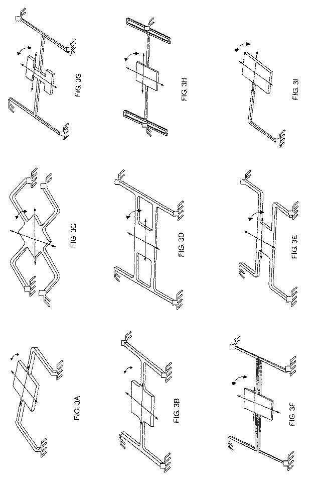
先に検討された寸法および測定値が単に例示の実施形態をもたらすものであり、また、かなりの変更が可能である、ということはわかるであろう。図3A〜図3Iは、共鳴センサー130についての代わりの有用な幾何学的形態を示している。本発明によって作られたセンサーチップ120では、すべての共鳴センサーを同じ幾何学的形態を用いて作ることができ(例えば、すべてを図2A〜図2Cに示されたように構成することができ)、あるいはこれに代えて、同じチップ上に相異なる共鳴センサーを相異なる幾何学的形態を用いて作ることができる(例えば、半分の共鳴センサーを図2A〜図2Cに示されたように構成することができ、残り半分の共鳴センサーを図3A〜図3Iに示された図形の1つ以上を用いて構成することができる)。
It will be appreciated that the dimensions and measurements discussed above are merely exemplary embodiments and that considerable changes are possible. 3A-3I illustrate alternative useful geometries for the
作動の際に、基板は、(例えば、図1Aおよび図1Bに示されたアクチュエーター160によって)0.1〜10MHzのような低振動数で揺動状に規制微量だけ動くことができる。基板のこのような動きによって、共鳴センサーの可動部材の動きが引き起こされる。可動部材132の共鳴振動数はその中央部材132の質量の関数である。測定対象が中央部材の受容体区域140に結合すると、測定対象の付加質量によって、その可動部材が共鳴を呈する振動数が変化する。同じように、測定対象が中央部材の受容体区域140から離脱すると、測定対象の除去質量によって、その可動部材が共鳴を呈する振動数が変化する。したがって、試料の中における測定対象の存在あるいは不存在は、センサーが試料にさらされた後の中央部材の共鳴振動数を監視することによって検出することができる。例えば、測定対象の存在は次の式(1)によって一般に検出することができる。
In operation, the substrate can move in a swaying manner at a low frequency such as 0.1-10 MHz (eg, by the
ΔM/M ∝ Δf共鳴/f共鳴 ……(1)
ここで、Mは中央部材132の質量、ΔMは測定対象が中央部材132に結合したときの質量の変化量、f共鳴は測定対象が受容体区域140に結合しなかったときに中央部材132が呈する共鳴での振動数、Δf共鳴は(質量ΔMの)測定対象が受容体区域140に結合したことによって引き起こされた共鳴振動数の変化量である。式(1)によれば、質量の変化を振動数の変化に関連付ける理想的表示がもたらされ、また、このような理想的観点には、共鳴器のそれぞれのモードについての同じような表示がさらに含まれる。
ΔM / M ∝ Δf resonance / f resonance ...... (1)
Here, M is the mass of the
図2A〜図2Cに示されたセンサー130の可動部材132は多重モード共鳴を呈する。すなわち、中央可動部材132の動きは、区別できる3つの揺動運動、例えばX方向における実質的揺動、Y方向における実質的揺動、およびシータ方向における実質的揺動(すなわち回転揺動)に分解することができる。これらの方向の独立した組み合わせからなるモードも設計によって可能である。中央可動部材が基板の近くに配置されているので、面外共鳴モード(例えばZ方向における共鳴動作)は、この隙間にある流体によってもたらされた損失によって制限される。中央可動部材を単一モードの場合よりもいっそう揺動させることによって、システム100の雑音排除性が有利に改善される。理想的には、受容体区域に結合された測定対象の存在あるいは不存在は中央可動部材の共鳴振動数に影響を及ぼす唯一の因子であるのがよい。しかしながら、中央可動部材の共鳴振動数は環境因子(例えば温度)によっても影響を受ける。いくつかの方向における揺動が他の方向における揺動よりも環境因子によっていっそう影響を受けるので、多重モード共鳴によって雑音排除性が改善され、また、環境の影響は測定対象の影響とは独立に解明することができる。
The
一例として、Y方向に延びるテザー(135,136)は、X方向に延びるテザー(137,138)に比べると、熱的影響のために構造的特性の顕著な変化を呈する。両方とも、温度変化によって引き起こされた弾性率の変化による同一の剛性変化を反映する。しかしながら、テザー135,136は、いずれの端部でも基板に事実上留められており、また、基板とテザー材料との間の異なる膨脹率に起因する変動張力(あるいは圧縮力)を受ける。この応力は、テザー135,136を曲げることによってテザー137,138で解除される。したがって、可動部材132のY平行移動モードは、温度変化による共鳴振動数の相対変位がX平行移動モードよりも大きい。両者は測定対象の質量積載のために同一の相対変位を生じる。そこで、両者の共鳴振動数の変化(すなわち、X方向およびY方向の両方における可動部材132の共鳴振動数の変化)を測定することで、測定対象の影響を温度誘発効果から区別することができる。
As an example, a tether (135, 136) extending in the Y direction exhibits a significant change in structural properties due to thermal effects compared to a tether (137, 138) extending in the X direction. Both reflect the same stiffness change due to the change in modulus caused by the temperature change. However, the
図2Aおよび図2Bには、受容体区域140を画成する中央可動部材132が示されているが、図示の便宜のために、受容体区域140は部材132にわたって均等に分布されている。しかしながら、受容体区域140は、より複雑に構成されているのが普通である。図4Aは、単一の中央可動部材132にわたって分布された受容体区域140の概念図を示している。図示されたように、受容体区域140には一連の結合部位410が含まれており、これらの結合部位410は一連の阻止部位420に点在されている。結合部位410および阻止部位420の詳細な構成、および阻止部位420が含まれる根拠は、以下で検討される。個々の受容体部位および阻止部位の縮尺は図4Aに示されたものよりもはるかに小さい、ということを認識すべきである。それぞれの受容体部位410は通常、測定対象の単一分子と同じような寸法のものであり、また、それぞれの阻止部位420は同じような寸法にされている。いくつかの実施形態には、中央可動部材132以外のセンサー構成要素の少なくとも一部に結合用および/または阻止用の物質からなるコーティングが含まれていてもよい、ということも認識すべきである。1つの代表的実施形態には、阻止用物質で被覆されたテザーが含まれていて、それらのテザーにおける物質の望ましくない堆積が防止されるようになっている。一般に、阻止用物質および結合用物質はセンサーの中央可動部材に必ずしも限定されない。
2A and 2B show the central
理想的には、あらかじめ選択された測定対象だけが結合部位410に結合し、どのような試料も結合部位410以外の可動部材132の区域に結合しないのがよい。しかしながら、典型的には、試料からの好ましくない物質(例えば蛋白質)が結合部位410以外の部位で可動部材132に結合する。阻止部位420は、受容体部位410以外の部位で可動部材132に結合する試料からの物質の量を減らすように含まれている。さらに理想的には、阻止部位420には何も結合しないのがよい。しかしながら、阻止部位420は受容体部位410以外の可動部材132の区域に結合する物質の量を減らすものの、試料からの何らかの物質が阻止部位420になお広く結合する。図4Bは受容体区域140を構成するための1つの方策を示しており、この方策によって、測定対象の効果と阻止部位に結合する好ましくない物質の効果との識別が可能になる。図4Bに示されたように、可動部材132の上には、離れた2つの受容体区域である第1受容体区域140Aと第2受容体区域140Bとが設けられている。第1受容体区域140Aは可動部材132の中央に位置している。図4Aに示された受容体区域140と同様に、第1受容体区域140Aには、一連の結合部位410が含まれており、これらの結合部位410は一連の阻止部位420に点在されている。しかしながら、第1受容体区域140Aは、可動部材132の外周辺まで延びておらず、代わりに、部材132の中央の近傍に配置されている。第2受容体区域140Bは、阻止部位420だけを含んでおり、また、第1受容体区域140Aの周辺の周りに配置されている。
Ideally, only a preselected measurement object will bind to the
作動の際に、好ましくない物質が第1受容体区域140Aにおける阻止部位420に結合すると、同じ種類の好ましくない物質も第2受容体区域140Bに結合しやすくなる。可動部材132の中央から距離があるため、第2受容体区域140Bに結合する物質の質量は、センサー130の回転共鳴モード(すなわち、シータ方向における中央可動部材の揺動)において顕著な効果を有している。これによって、この測定システムは、結合部位410に結合する測定対象と阻止部位420に結合する好ましくない物質とを識別することができる。
In operation, if undesired material binds to the
可能性のある4つの事例の簡単な検討によって、有用な識別をもたらすために図4Bに示された受容体区域の構成をどのように用いることができるかが一般に例示される。第1の事例では、試料の中に測定対象が実質的に存在せず、また、試料からは何も阻止部位420に結合しない。この事例では、可動部材の共鳴振動数は試料へさらされることによって実質的に変化しない。第2の事例では、試料の中に測定対象が存在しており、また、試料の中からは実質的に何も阻止部位420に結合しない。この事例では、測定対象は受容体部位410に結合し、それによって、X方向およびY方向における可動部材の共鳴振動数が変化する。試料へさらされることによって質量が阻止部位420に付加されないので、回転揺動の振動数は、試料へさらされることによって比較的小さい変化だけを受ける。第3の事例では、試料の中には測定対象が実質的に存在しないものの、試料からの物質が阻止部位420に結合する。この事例では、阻止部位420に結合する物質の質量は、X方向、Y方向およびシータ方向における可動部材の共鳴振動数に影響を及ぼす。第4の事例では、試料の中には測定対象が存在しており、また、試料からの物質も阻止部位420に結合する。この事例では、受容体部位410および阻止部位420に結合する物質の質量は、X方向、Y方向およびシータ方向における可動部材の共鳴振動数に影響を及ぼす。第3の事例の結果と第4の事例の結果とは類似しているが、X方向およびY方向における共鳴振動数の変化は、第4の事例の方が第3の事例よりも大きい(すなわち、受容体部位410に結合した測定対象の付加質量があるので)。かなりの変形が可能であるが、これら4つの事例では、受容体部位410に結合する測定対象と阻止部位420に結合する好ましくない物質とを識別するための基本的方策が説明されている、ということが分かるであろう。以下の表はこれらの事例を要約している。
A brief review of the four possible cases generally illustrates how the receptor area configuration shown in FIG. 4B can be used to provide useful identification. In the first case, there is substantially no measurement object in the sample, and nothing from the sample binds to the
先に検討されたように、この感知システム100によれば、このシステムが試料にさらされた後に共鳴センサー130の共鳴振動数を監視することで、試料の中における特定の測定対象の存在を検出することができる。共鳴センサーの共鳴振動数だけを監視する簡単な方法は、感知システム100を使うための有効な手段である。しかしながら、それは、感知システム100から得ることのできる情報の簡単で退歩した事例であることも意味している。この情報のいっそう完全な説明は図12Aおよび図12Bに示されているが、これらの図は、特定方向(例えばX方向)に測定された単一の共鳴センサー130における振動数特性の大きさおよび位相を示すグラフである。図12Aおよび図12Bに表示された情報をどのように用いるかを検討する前に、これらのグラフが作成される方法について説明する。
As previously discussed, the
図2A〜図2Cに戻ると、基板126が特定の振動数で揺動状に動くと、共鳴センサー130の可動部材132もまた、実質的に同じ振動数で揺動状に動き始める。しかしながら、共鳴センサー130の2つの有意パラメーターである、(1)可動部材132の揺動の振幅と基板126の揺動の振幅との比、すなわち振動数特性の「大きさ」、および(2)可動部材132の揺動と基板126の揺動との位相差、すなわち振動数特性の「位相」は、基板126の揺動振動数によって変化する。図12Aは振動数特性の大きさを示している(すなわち、基板126の揺動振動数の範囲について、同図は可動部材132の揺動の振幅を基板126の揺動の振幅で割ったものを示している)。図12Bは振動数特性の位相を示している(すなわち、基板126の揺動振動数の範囲について、同図は可動部材132の揺動と基板126の揺動との位相差を示している)。また、先に述べたように、図12Aおよび図12Bに示された振動数特性は、X方向のような特定の方向に測定された特性を表している。3つの主要共鳴モード(例えば、実質的にX方向、Y方向およびシータ方向における揺動)を呈する共鳴センサー130については、共鳴センサー130の振動数特性を充分に特徴付けるために、図12Aおよび図12Bに示されたグラフの形態にある三組のグラフを作成することができる(すなわち、一組はX方向、Y方向およびシータ方向における振幅特性および位相特性を示している)。
2A to 2C, when the
図12Aに示されたように、振動数特性の大きさ(少なくとも単一方向に測定された)は、共鳴振動数frでピークを示している。また、図12Bに示されたように、振動数特性の位相は、共鳴振動数frの近くで急激な変化を示している。図12Aおよび図12BがX方向における可動部材132の揺動についての振動数特性の振幅および位相を表しているときには、Y方向およびシータ方向における可動部材の特性を示すグラフは、特徴が図12Aおよび図12Bにほぼ類似しているように見えるであろうが、典型的には異なった共鳴振動数(すなわちfrとは異なる)でピークを示すであろう。
As shown in FIG. 12A, the magnitude of the frequency characteristics (measured in at least one direction) shows a peak at the resonance frequency f r. Further, as shown in FIG. 12B, the frequency characteristic phase indicates the abrupt change in the vicinity of the resonance frequency f r. When FIG. 12A and FIG. 12B represent the amplitude and phase of the frequency characteristic for the swing of the
図12Aおよび図12Bは特定条件下における共鳴センサー130の振動数特性を表している。例えば、図12Aおよび図12Bは、感知システム100が測定対象を含有している試料にさらされる前の共鳴センサー130の振動数特性を示していてもよい。感知システム100が測定対象を含有している試料にさらされると、センサー130の振動数特性は変化する(すなわち、振動数特性は、可動部材132の受容体区域に結合する何らかの測定対象を有していることに応じて変化する)。例えば、測定対象含有試料にさらされた後には、センサーの振動数特性はさらされる前の特性に類似しているのが普通であるが、共鳴が起きる振動数は変わる(すなわち、共鳴のピークはfr+デルタにある)。
12A and 12B show the frequency characteristics of the
先に述べたように、試料の中における測定対象の存在は、共鳴センサー130の可動部材132の共鳴振動数を監視することで容易に検出することができる。同じように、試料の中における測定対象の存在は、特定の揺動振動数で共鳴センサー130の振動数特性を監視することで(すなわち、特定の一定振動数でセンサーチップを揺動させることで、また、その振動数で共鳴センサーの振動数特性を監視することで)、容易に検出することができる。
As described above, the presence of the measurement target in the sample can be easily detected by monitoring the resonance frequency of the
しかしながら、特定の一定振動数で振動数特性を監視する代わりに、振動数の全範囲にわたって共鳴センサーの振動数特性を監視することは有利である。このことによって、単一のあるいは少数のデーターポイントではなくデーターポイントの集合に基づいて、試料中に測定対象が存在しているかどうかを決定することができる。換言すると、離れたデーターポイントを試験するのに代えて、この技術によれば、全範囲にわたって関数を試験することができる。例えば、共鳴センサーの振動数特性の振幅および位相は、振動数の全範囲にわたって測定することができ、また、測定された特性は、あらかじめ決められた一組以上の振動数特性あるいはその曲線適合関数と比較することができる。振動数特性のそれぞれは基板の揺動振動数および他の変数の関数である。あらかじめ決められた振動数特性は、(1)感知システムがどのような試料にもさらされず、したがって「製造したての」状態にある事例、(2)感知システムが測定対象を含有している試料にさらされ、かつ、試料が受容体区域の阻止部位へ結合しない種類のものである事例、および(3)感知システムが測定対象を含有している試料にさらされ、かつ、試料が受容体区域の阻止部位へ結合する種類のものである事例のようなさまざまな事例を表すことができる。他の多くの事例についての振動数特性あるいはその曲線適合関数をあらかじめ準備することができるということと、作動の際に測定された振動数特性をこれらの特性および関数と比較することができるということとは分かるであろう。どの事例が感知システムによって受けた状態を実際に表しているかについての決定は、測定された振動数特性をあらかじめ決められた事例の振動数特性と比較してその最良の組み合わせを選択することによって行われる。 However, instead of monitoring the frequency characteristics at a specific constant frequency, it is advantageous to monitor the frequency characteristics of the resonant sensor over the entire range of frequencies. This makes it possible to determine whether a measurement object is present in a sample based on a collection of data points rather than a single or a small number of data points. In other words, instead of testing distant data points, this technique allows the function to be tested over the entire range. For example, the amplitude and phase of the frequency characteristics of the resonant sensor can be measured over the entire range of frequencies, and the measured characteristics can be a predetermined set of frequency characteristics or a curve fitting function thereof. Can be compared. Each of the frequency characteristics is a function of the oscillation frequency of the substrate and other variables. The predetermined frequency characteristics are: (1) a case where the sensing system is not exposed to any sample and therefore in a “freshly manufactured” state, (2) a sample where the sensing system contains the object to be measured And the sample is of a type that does not bind to the blocking site of the receptor area, and (3) the sensing system is exposed to the sample containing the measurement object, and the sample is in the receptor area Various cases can be represented, such as those that are of the type that bind to the blocking site. The frequency characteristics or curve fitting functions for many other cases can be prepared in advance, and the frequency characteristics measured during operation can be compared with these characteristics and functions. You will understand. The decision as to which case actually represents the condition received by the sensing system is made by comparing the measured frequency characteristics with the predetermined case frequency characteristics and selecting the best combination. Is called.
あらかじめ決められた振動数特性は1つ以上の制御用共鳴センサーを用いて準備することができる、ということも分かるであろう。制御用共鳴センサーは、特定の測定対象の存在について試験するために後に使われる共鳴センサーを製造するために用いられたのと同じ処理によって製造することができ、それによって、それらは実質的に類似した振動数特性を呈する。この代わりに、そのような制御用共鳴センサーを使う必要なしに、あらかじめ決められた特性を、試料の中における測定対象の存在あるいは不存在を検出するために後に使われるものと同じセンサーを使って、測定することができる。 It will also be appreciated that the predetermined frequency characteristic can be prepared using one or more control resonance sensors. Controlling resonance sensors can be manufactured by the same process used to manufacture a resonance sensor that is later used to test for the presence of a particular measurement object, so that they are substantially similar. Exhibit frequency characteristics. Instead of using such a control resonance sensor, a predetermined characteristic can be obtained using the same sensor that is later used to detect the presence or absence of the measurement target in the sample. Can be measured.
複数のセンサーを同じ測定対象についての異なる受容体分子で構成することができる、ということも分かるであろう。例えば、単一の測定対象の異なったエピトープについての異なった抗体特性を用いることができる。このことは、測定対象の検出における信頼度を増大させるために有用である。 It will also be appreciated that multiple sensors can be constructed with different receptor molecules for the same analyte. For example, different antibody characteristics for different epitopes of a single measurement can be used. This is useful for increasing the reliability in detecting the measurement object.
試料の中における測定対象の存在を検出するために感知システム100を使う数々の方法がこれまで検討されてきた。測定対象の存在を検出するのに加えて、感知システム100は、試料の性質を測定するためにより広く使うことができる。例えば、感知システム100が油の中に沈められると、感知システム100は油の粘度を決定するために使うことができる。受容体区域へ結合する測定対象によって共鳴センサー130の可動部材132に質量が付加されるのに対して、共鳴センサー130を包囲する油によって、中央可動部材132の動きに対する抵抗がもたらされる(たとえ、油がセンサーに結合しないときでも、またセンサーに選択的結合のための受容体区域が含まれていないときでも)。油によって加わった抵抗の大きさは油の粘度の関数である。そこで、油の粘度は、可動部材の動きが油の存在によって影響を受ける態様を監視することで測定することができる。一般に、感知システム100は、試料(例えば、油、特定の測定対象が含有されている気体など)と1つ以上の共鳴センサー130との間の相互作用を測定するために使うことができる。
A number of methods that use the
図5はセンサーチップ120を製造するための処理500を説明するフローチャートを示している。図6A〜図6Iは、処理500のさまざまな段階で製造された中間製品を示している。
FIG. 5 shows a flowchart illustrating a
処理500における第1ステップ510は絶縁体上シリコン(SOI)ウェーハを用意するためのものである。このようなSOIウェーハ610は図6Aに示されている。示されたように、ウェーハ610には、シリコン基板612と、シリコン基板612の上に重なっている二酸化ケイ素のような絶縁層614と、絶縁層614の上に重なっているシリコンデバイス層616(例えば単結晶シリコン)とが含まれている。1つの実施形態では、デバイス層616は厚さが4ミクロンであり、絶縁層614は厚さが3ミクロンであり、基板612は厚さが約500ミクロンである。
A
処理500における第2ステップ512はデバイス層に隆起区域を形成するためのものである。図6Bはこのステップの成果を示している。示されたように、ここではデバイス層616に隆起区域618が画成されている。隆起区域618はデバイス層616の底面619の上方に約2ミクロン立ち上がっている。処理の後の段階で、隆起区域618は図2A〜図2Cに示されたアンカー134を形成するために用いられる。隆起区域618は従来のフォトリソグラフィー処理法を用いて形成してもよい。例えば、フォトレジストで覆われなかったデバイス層を2ミクロンの深さまでエッチングするために、時間調節エッチング法を用いることができる。反応性イオンエッチング剤(RIE)およびフォトレジストマスクがこのステップのために適している。この代わりに、結晶シリコンエッチング法を用いることもできる。いっそう後の処理によって可動部材の底部における製作完了後の静止摩擦が防止される表面619の上に特徴部を設けるために、この時点で別のエッチングステップを挿入することができる。これらの特徴部は、可動部材が基板に触れる接触区域を制限するための小さい突起であり、これらの突起は、接合力をその接合力がテザーの復元力よりも小さくなるように制限する。このステップでは、先に説明したのと同じフォトレジストマスキングおよびRIEステップが用いられる。処理500における次のステップ514はシリコン構造体を画成するためのものであり、このシリコン構造体は、エッチングによってデバイス層616を絶縁層614まで低くすることで後に可動部材を構成する。このステップの成果は図6Cに示されている。示されたように、このステップの後には、隆起区域618は残っているが、デバイス層の一部は構造体620を画成するために除去されている。構造体620は、ここでは絶縁層614に固定されているが、処理500における後のステップでは、構造体620は中央可動部材(例えば、図2Bにおける132で示されたようなもの)になる。この処理ステップ514では、次の諸構造体、すなわち、アンカーになる隆起区域618と、可動部材になる構造体620と、構造体620をアンカーに連結するテザー(図6Cには示されていないが、図6Iには示されている)とがエッチングされるのを防止するために、フォトレジストが使われる。このステップ514のエッチングを行うためには反応性イオンエッチングが適しており、また、絶縁層614はエッチング停止部として作用することができる。
The
処理500における次のステップ516は構造体620の上に金属構造体を形成するためのものである。このステップの成果は図6Dに示されている。図6Dに示されたように、構造体620の上に金属細長片622が形成されている。金属細長片622によって、可動部材の位置を感知するために使われる光学格子が形成されている。細長片622はアルミニウムのような反射性金属から形成することができる。細長片622を形成するための1つの方法は、(a)細長片622が形成されると好ましくない区域における構造体620の上にフォトレジストを被着させ、(b)電子ビーム蒸発器あるいは類似システムを使って、構造体620およびその上に重なっているフォトレジストの上に、0.1ミクロンの厚さが適切であるアルミニウムの薄い層を被着させ、その後、(c)ウェーハを溶媒の中に浸漬させて、フォトレジストとフォトレジストの上にある金属とを除去し、それによって、所望の細長片622を得ることである。細長片622を形成するこの方法は「リフトオフ」法と称されるが、その理由は、金属層における好ましくない部分が、下にあるフォトレジストを除去するための浸漬によって構造体から「引き上げ」、すなわち除去されるからである。
The
処理500における次のステップ518はガラス基板の上に金属構造体を形成するためのものである。このステップの成果は図6Eに示されている。示されたように、金属細長片624がガラス基板626の上に被着されている。金属細長片624によって、可動部材の位置を感知するために使われる光学格子が形成されている。ガラス基板626の材料についての1つの良好な選択は、ニューヨーク州、コーニングのコーニング(Corning)社から市販されている#7740(パイレックス)ガラスである。この材料は、シリコンとの間で強い陽極結合を形成することができる点で好ましい。金属細長片624は、ステップ516に関して先に検討されたのと同様な「リフトオフ」法を用いて、基板626の上に形成することができる。
The
処理500における次のステップ520は、ステップ516(すなわち、図6Dに示されたステップ)の終わりに製造された構造体を逆さにし、それをステップ518(すなわち、図6Eに示されたステップ)の終わりに製造された構造体に接合するためのものである。このステップの成果は図6Fに示されている。示されたように、隆起シリコン部分618はガラス基板626の上面に接合されている。このステップの終わりには、構造体620の上に形成された光学格子622が、基板626の上に形成された光学格子624にほぼ対向している。隆起シリコン部分618は、構造体を180〜500℃まで加熱し、接合区域にわたって200〜1000ボルトの電位を印加することで、ガラス基板626に接合することができる。これらの状態において、約10分で強力な接合が達成される。
The
処理500における次のステップ522はSOI構造体から「把手型ウェーハ」を除去するためのものである。この処理の成果は図6Gに示されている。示されたように、把手型ウェーハ612は絶縁層614から除去されている。把手型ウェーハ612を除去するためには、液体エッチング、プラズマエッチング、あるいはフッ化キセノン(XeF2)のような気体状シリコンエッチング剤によるエッチングのようなさまざまな方法を用いることができる。
The
処理500における次のステップ524はSOIウェーハの残部から絶縁層614を除去するためのものである。このステップの成果は図6Hに示されている。絶縁層614はプラズマエッチングによって除去してもよい。この時点で、構造体620は、動くために自由にされており、今や、共鳴センサーの中央可動部材(例えば、図2Bにおける132で示されたようなもの)として作用することができる。図6Iは、図6Hに示されたような矢印6I−6Iの方向に沿ったこの構造体の図を示している。示されたように、構造体620は、図2Bに示されたセンサーにおけるようなテザーによってアンカーに連結されている。図6Iに示されたテザーは、テザーを構成するシリコン材料をステップ514で行われたエッチングステップから保護することで画成された。
The
処理500における次のステップ526は可動部材620の上に受容体区域622を形成するためのものである。受容体区域622を形成するための処理は以下でさらに検討される。しかしながら、この処理には、可動部材構造体620の上にチタンと金の層を被着させることが含まれていてもよい。金は受容体部位を形成するために有用であり、チタンは金をシリコン構造体622へ接合するために有用である。
The
処理500における諸ステップは、単一の共鳴センサーがその上にある単一のセンサーチップを形成することに関して検討されてきたが、この処理500は複数のセンサーチップを形成するために用いることができ、また、それぞれのチップには複数の共鳴センサーが含まれていてもよい、ということは分かるであろう。ウェーハ処理が完了した後に、ウェーハはたいていダイソーを使って個々のチップに裁断される。可動微細構造体はウェーハダイシングの間に保護されるのが好ましい。この目的のためには、実質的に除去されるフォトレジストの層が一般に適している。
Although the steps in
図7A〜図7Gは、センサーチップ120を形成するための別の処理におけるさまざまな段階で製造された中間製品を示している。この処理は「溶解ウェーハ処理」と称することができる。図7Aに示されたように、この処理はシリコンウェーハを調達することで始まる。処理500とは異なり、SOIウェーハは溶解ウェーハ処理には使われない。
FIGS. 7A-7G show the intermediate product manufactured at various stages in another process to form the
図7Bに示されたように、次いでウェーハの上面がエッチングされて、底面719の上方に立ち上がる隆起区域718が作られる。隆起区域718の幾何学的形態および寸法は図6Bに示された隆起区域618のそれらに類似しており、また、隆起区域718は後に共鳴センサーのアンカーを構成する。図7Cに示されたように、次いで隆起区域718どうしの間におけるウェーハの一部にホウ素を吹き込むことで、構造体層716が画成される。
As shown in FIG. 7B, the top surface of the wafer is then etched to create a raised
図7Dに示されたように、次いで構造体層716の一部がエッチングされて構造体720が画成される。付加的処理の後に、構造体720は共鳴センサーの中央可動部材を構成する。アンカーを中央可動部材に連結するテザーも、このエッチングによって画成される。テザーを示す図6Iは、図7Dに示された構造体の一般的外観の平面図を示している。図7Dに示されたように、光学格子を形成する金属細長片722も構造体720の上面に形成されている。
As shown in FIG. 7D, a portion of
図7Eに示されたように、光学格子を形成する金属細長片624がガラス基板の上に形成されている。このステップは処理500のステップ518と同一である。
As shown in FIG. 7E, a
図7Dに示された構造体は次いで逆さにされて、図7Eに示された構造体に接合される。この接合は、処理500のステップ520に関して検討されたように実施することができる。図7Fはこの接合ステップの後に形成された構造体を示している。
The structure shown in FIG. 7D is then inverted and joined to the structure shown in FIG. 7E. This bonding can be performed as discussed with respect to step 520 of
図7Gに示されたように、次いでホウ素が吹き込まれなかったウェーハ712の一部が溶解される。この目的のためにはエチレンジアミンピロカテコール(EDP)のような選択エッチング剤を用いることができる(例えば、1992年発行のJ. MEMS 第1巻第2号のGianchandani, Y.B. および Najafi, K. による“A bulk silicon dissolved wafer process for microelectromechanical devices”に説明されたように)。それらは相異なる処理によって作られるが、図7Gに示された構造体と図6Hに示された構造体とは類似している。組み立ては、構造体720の上に受容体区域を形成し、その後にウェーハを裁断して個々のセンサーチップを形成することで完了する。
As shown in FIG. 7G, the portion of
図8A〜図8Fは、センサーチップ120を形成するためのさらに代わりの処理におけるさまざまな段階で製造された中間製品を示している。図8Aに示されたように、この処理はシリコンウェーハ812を調達することで始まる。
8A-8F illustrate intermediate products manufactured at various stages in a further alternative process for forming
図8Bに示されたように、次いで基板812を覆って犠牲層850が形成される。犠牲層850は例えば二酸化ケイ素から形成することができる。
A
図8Cに示されたように、次いで層850の選択された部分にエッチングで穴852が形成される。ここで、その後に形成される中央可動部材の位置に対応した領域における二酸化ケイ素にくぼみを形成するために、追加エッチング処理を加えてもよい。この目的のためには、フッ化水素酸を使う時間調節エッチングを用いることができる。犠牲層の上面に構造体層が正角状に被着されると、離脱の後の静止摩擦を防止するために突起が形成される。
As shown in FIG. 8C, holes 852 are then etched in selected portions of
図8Dに示されたように、次いで犠牲層850を覆ってシリコン層860が形成される。この層860は、被着したシリコンが先のエッチングで層850に形成された穴852を塞ぐように、形成される。被着したシリコンは、図8Cに関連して先に検討された追加エッチング処理によって犠牲層850に先に形成されたくぼみも塞ぐ。追加処理の後に、穴852を塞いだシリコンは共鳴センサーのアンカーを構成することになる。
As shown in FIG. 8D, a
図8Eに示されたように、次いでシリコン層860を覆って金属部870が形成される。追加処理の後に、金属部870は共鳴センサーの受容体区域の一部を構成することになる。
As shown in FIG. 8E, a
図8Fに示されたように、次いでシリコン層860の一部がエッチングされて、可動部材860(およびテザー)が画成されるとともに犠牲層850の一部が露出される。犠牲層はその後のエッチングステップ(例えば、フッ化水素酸を使う二酸化ケイ素のエッチング)によって除去されて、可動部材が離脱される。この離脱処理に必要な時間を短縮するために、中央可動部材の中に穴をエッチングで形成してもよい。これらは、光学変換処理を妨げないように、充分小さくかつ良好に間隔を置いて行ってもよい。このエッチングステップによって、可動部材と、可動部材をアンカー890に連結するためのテザー(図示略)とが作られる。この場合もやはり、これらは異なった処理によって作られるが、図6Iに示された構造体と図8Fに示された構造体とは類似している。しかしながら、図6Iに示された構造体とは異なり、図8Fに示された構造体には、可動部材の位置を感知するために使うことのできる光学格子が含まれていない。可動部材880の位置を感知するためには、以下で検討される他の感知方式を用いることができる。
As shown in FIG. 8F, a portion of the
可動部材、アンカーおよびテザーをニッケル、鉄、鉄−ニッケル合金、銅あるいは金のような金属から作ることもできる。これらの構造体を形成するためにはメッキ処理が有利であるが、その理由は作られる金属層が低い応力水準と予測可能な諸性質とを有する傾向にあるからである。この製作法は、シリコン、セラミック(例えば窒化アルミニウム)あるいはガラス(例えばパイレックス)からなるウェーハのような平坦な基板で始められる。基板の上には薄い導電性種子層が被着される。例えば、2000オングストロームの金で覆われる500オングストロームのクロムが適している。他の金属層の組み合わせおよび厚さを用いることができる。さらに、この層は、必要であれば、標準的なフォトリソグラフィー法を用いてパターン化することができる。その後、種子層を覆って光活性化ポリマー(例えば、フォトレジスト、ポリイミド)の層が被着され、次いでアンカーの位置を画成するためにパターン化される。次いで、ニッケルのような金属部が、パターン化されたフォトレジストによって画成された穴を金属部で塞ぐように、電気メッキで形成される。この金属部は、アンカーの高さ、すなわち可動部材と基板との隙間を画成するために、所望の厚さで形成される。この厚さはポリマー層の高さにほぼ一致している。したがって、必要であれば、金属アンカーおよびポリマーは平坦化してもよい。次いで、アンカーおよびポリマーフォトレジストを覆って、金属からなる第2種子層が形成される。この第2種子層はその後パターン化されて、テザーおよび中央可動部材の形状が画成される。次いで、この第2種子層を覆って、ポリマーからなる第2フォトレジスト層が被着される。第2フォトレジスト層は次いでパターン化されて、第2種子層が露出する(すなわち、テザーおよび可動部材が形成される部位が露出する)。パターン化された第2フォトレジスト層は、テザーおよび中央可動部材を形成するためのモールドとして有効に作用する。次いで電気メッキ法を用いて、第2種子層を覆う、より厚い金属層が形成される。このより厚い金属層はテザーおよび中央可動部材を形成する。メッキ時間は、テザーおよび中央可動部材が所望の厚さになるのを保証するために調節される。必要であれば、表面粗さを減少させるために、上面を平坦化してもよい。先の製作法について説明されたように、受容体を取り付けかつ/または光学的感知を促進するために、中央可動部材の上面に仕上げ金属層(例えば金)をパターン形成することができる。次いで、フォトレジストを除去するために、また、金属製中央可動部材が基板に関して動くようにするために、溶剤が用いられる。金属から構成された可動部材を作るためのここで説明された処理はただ1つの例に過ぎない。いっそう進歩したメッキ法には、LIGA法やカリフォルニア州、バーバンクのMEMGen社から得ることのできるEfab法が含まれる。
Movable members, anchors and tethers can be made from metals such as nickel, iron, iron-nickel alloys, copper or gold. Plating is advantageous for forming these structures because the metal layer produced tends to have low stress levels and predictable properties. This fabrication method begins with a flat substrate such as a wafer made of silicon, ceramic (eg, aluminum nitride) or glass (eg, Pyrex). A thin conductive seed layer is deposited on the substrate. For example, 500 angstroms of chromium covered with 2000 angstroms of gold is suitable. Other metal layer combinations and thicknesses can be used. Furthermore, this layer can be patterned using standard photolithographic methods if desired. A layer of photoactivatable polymer (eg, photoresist, polyimide) is then deposited over the seed layer and then patterned to define the location of the anchor. A metal part, such as nickel, is then formed by electroplating so as to plug the hole defined by the patterned photoresist with the metal part. This metal part is formed with a desired thickness in order to define the height of the anchor, that is, the gap between the movable member and the substrate. This thickness approximately corresponds to the height of the polymer layer. Thus, if necessary, the metal anchor and polymer may be planarized. A second seed layer made of metal is then formed over the anchor and polymer photoresist. This second seed layer is then patterned to define the shape of the tether and the central movable member. Next, a second photoresist layer made of polymer is deposited over the second seed layer. The second photoresist layer is then patterned to expose the second seed layer (i.e., the site where the tether and movable member are formed). The patterned second photoresist layer effectively acts as a mold for forming the tether and the central movable member. A thicker metal layer is then formed using electroplating to cover the second seed layer. This thicker metal layer forms the tether and the central movable member. The plating time is adjusted to ensure that the tether and central movable member are of the desired thickness. If necessary, the top surface may be planarized to reduce surface roughness. As described for previous fabrication methods, a finish metal layer (eg, gold) can be patterned on the top surface of the central movable member to attach the receptor and / or facilitate optical sensing. A solvent is then used to remove the photoresist and to allow the metal central movable member to move relative to the substrate. The process described here for making a movable member composed of metal is only one example. More advanced plating methods include the LIGA method and the Efab method available from MEMGen, Burbank, California.
図1Aに関連して先に検討されたように、光学系180によって、センサーチップ120の上の共鳴センサー130が監視される。さらに詳しく言えば、光学系180によって、共鳴センサーの中央可動部材の瞬間位置が監視される。長時間にわたってこの瞬間位置を測定することで、この測定システムによって可動部材の揺動振動数を決定することができる。長時間にわたって中央可動部材の瞬間位置を測定することで、この感知システムによって、揺動運動が減衰する損失あるいは速度のような可動部材の他の特性を決定することができる。
As discussed above in connection with FIG. 1A, the
従来技術では、MEMS装置における可動部材の位置を監視するために、容量法、圧電抵抗法および圧電法のような他の非光学的対処法が用いられてきた。これらの方法は本発明に用いることができる。しかしながら、光学的監視は、導電性溶液(例えば試料中の塩)の存在によって影響されない点で有利である。 In the prior art, other non-optical measures such as capacitive, piezoresistive and piezoelectric methods have been used to monitor the position of the movable member in the MEMS device. These methods can be used in the present invention. However, optical monitoring is advantageous in that it is not affected by the presence of a conductive solution (eg, a salt in the sample).
図2A、図6Iおよび図7Gに示されたように、共鳴センサーは、対向状に配置された2つの光学格子(一方の光学格子は中央可動部材の表面に配置され、他方の光学格子は下にある基板の表面に配置されている)を含むように作ることができる。これらの光学格子によって、光学系180が共鳴センサー130の中央可動部材の瞬間位置を監視することができる。さらに詳しく言えば、作動の際に、光源182から、共鳴センサーの光学格子の表面に入射する光の狭帯域連続ビームが放射される。光源182と共鳴センサーとの間に配置された構造体(例えば、基板あるいはマウントのようなもの)は、光源182によって放射された波長が透過するものであるのが好ましい。光学格子から回折された光は検出器184によって受光される。共鳴センサー130の可動部材の位置を決定するために、周知の光学技術によって、検出器184で受光された回折領域における強度分布を用いることができる。光学系184は一般に、中央可動部材が約1MHzの振動数で揺動するときに1オングストローム以下のように小さい可動部材の動きを検出することができる。
As shown in FIG. 2A, FIG. 6I and FIG. Arranged on the surface of the substrate). These optical gratings allow the
図2Cは、格子142の細長片がX軸およびY軸に対して45度に方位付けられていることを示している。この構成では、X方向およびY方向における可動部材の等しい変位によって、2つの光学格子(例えば、図2Aに示されたような格子142,144)の相対位置における同じ変化が作られる。したがって、両方の動きを変換するために単一の格子を使うことができる。2つのモードの共鳴振動数は異なるので、光検出器からの電気信号を2つの成分に分解するために電子フィルター法あるいは信号処理法(例えばフーリエ分解)を用いることができる。
FIG. 2C shows that the strips of
図9Aは共鳴センサーの可動部材を光学的に監視するための代わりの構造体を示している。図9Aに示されたセンサー900は図8Fに示された構造体に類似している。しかしながら、センサー900には、シリコン基板812に形成された2つのフォトダイオード910がさらに含まれている。このようなフォトダイオードを形成する方法は周知であり、例えば、1996年発行のJ. MEMS 第5巻第4号のPadmanabhan, A., Goldberg, H., Breuer, K.D., および Schmidt, M.A. による“A wafer-bonded floating-element shear stress microsensor with optical position sensing photodiodes”に説明されている。センサー900を形成するための処理は図8A〜図8Fに関連して説明された処理に類似しているが、しかしながら、犠牲層850を形成するのに先だってフォトダイオードが形成されている。
FIG. 9A shows an alternative structure for optically monitoring the movable member of the resonance sensor. The
作動に際して、センサー900は上方から照射され、フォトダイオードは可動部材とアンカーとの間の窓穴902を通る光を受ける。可動部材が動くと、窓穴902の大きさが変化し、それによって、フォトダイオードに入射する光の量が増大するかあるいは減少する。フォトダイオードによって、フォトダイオードに入射する光の量に対応する出力信号が作り出される。フォトダイオードによって作り出された出力信号は結果的に可動部材880の瞬間位置を表示するものである。これらの信号を長時間にわたって監視することで、この測定システムによって可動部材の揺動振動数を測定することができる。
In operation, the
1つの実施形態では、窓穴902の幅は公称では(すなわち、可動部材が静止しているときには)、5ミクロンである。この実施形態では、可動部材が1ナノメートルだけ変位すると、窓穴902の大きさは0.02%だけ変化する。フォトダイオードによって作り出された出力信号は一般に位相が不一致であり、信号対雑音比を改善するために区別をつけて検出することができる。図9Aに示されたように構成されたフォトダイオードは一般に、1ナノメートル未満である中央可動部材の変位を検出することができる。
In one embodiment, the
図9Bは、共鳴センサーの中央可動部材の揺動振動数を監視するためにフォトダイオードを使うことのできる別の構造体を示している。図9Bに示されたように、中央部材880は、アンカー890で基板に固定されたテザーによって支持されている。静止マスク882が可動部材880を広く包囲している。A、B、CおよびDで表された4つのフォトダイオードが可動部材880の隅の近くに配置されている。可動部材880と静止マスク882との間の窓穴を通る光がフォトダイオードによって受けられる。フォトダイオードAは可動部材880の南西隅(すなわち左下隅)のわずか上方であってその左に位置しており、フォトダイオードDは南西隅のわずか右であってその下方に位置しており、フォトダイオードCは可動部材の北東隅(すなわち右上隅)のわずか上方であってその左に位置しており、フォトダイオードBは北東隅のわずか下方であってその右に位置している。
FIG. 9B shows another structure in which a photodiode can be used to monitor the oscillation frequency of the central movable member of the resonance sensor. As shown in FIG. 9B, the
4つのフォトダイオードによって作り出された出力信号は、X方向、Y方向およびシータ方向における可動部材880の位置を表す信号を作るために、さまざまな方法で組み合わすことができる。一般に、フォトダイオードAによって作り出された出力信号とフォトダイオードBによって作り出された出力信号との差は、X方向(すなわち、A−Bによって表されたX位置)に測定された可動部材880の位置を表すものであり、フォトダイオードCによって作り出された出力信号とフォトダイオードDによって作り出された出力信号との差は、Y方向(すなわち、D−Cによって表されたY位置)に測定された可動部材の位置を表すものである。最後に、フォトダイオードCによって作り出された出力信号とフォトダイオードDによって作り出された出力信号との合計とフォトダイオードAによって作り出された出力信号とフォトダイオードBによって作り出された出力信号の合計との差は、可動部材880の回転方位(すなわち、(A+B)−(C+D)によって表された回転位置)を表すものである。これらの信号を長時間にわたって監視すると、X方向、Y方向およびシータ方向における可動部材880の揺動振動数の測定値がもたらされる。
The output signals produced by the four photodiodes can be combined in various ways to produce a signal that represents the position of the
図9Bに示された構造体は、センサー900(図9Aに示されたもの)を作るために用いられたものに類似した方法を用いて製作することができる。しかしながら、静止マスク882もまた形成される。静止マスク882は、可動部材を画成するのに用いられるエッチングステップの間にこれらの区域を保護するためにこれらの区域をフォトレジストで覆うことによって、形成することができる。さらに、これらの区域の横方向への広がりは、これらの区域の構造的一体性を維持するために離脱処理の間にこれらの区域が完全にはアンダーカットされないようなものである。
The structure shown in FIG. 9B can be fabricated using a method similar to that used to make sensor 900 (shown in FIG. 9A). However, a
共鳴センサーの中央可動部材の位置および揺動振動数を光学的に監視するためのさらに別の対処法は、同センサーをパルス光源(あるいはストロボ光源)で照射し、かつ、可動部材から反射した光を位相固定型画像処理システムで画像処理することである。この光のパルスは、中央可動部材の動きを効果的に凍結するために充分に短い継続時間のものである。同一位相で記録されたいくつかの画像は、雑音を減らすために平均化することができる。約10ナノメートルの振幅と約1MHzの振動数とがある可動部材については、可動部材を1ナノメートル変位させるために約10ナノ秒のパルス持続時間が用いられる。このことはさまざまなレーザー光源(例えば可視的半導体レーザー)で達成することができる。その反射光はCCDカメラの上に画像形成することができる。この対処法に基づいた画像処理システムは例えば、マサチューセッツ州、ウォータータウンのUMech Technologies社からMMA G2登録商標 MEMS Motion Analyzerとして市販されている。参照変位測定を促進するためには、センサーチップの可動部分および静止部分に反射特徴部を含めることができる。これによって、画像処理システムに対するこのアセンブリーの全体運動の阻止が促進される。 Still another way to optically monitor the position and oscillation frequency of the central movable member of the resonance sensor is to irradiate the sensor with a pulsed light source (or strobe light source) and reflect the light from the movable member Is processed by a phase-fixed image processing system. This pulse of light is of a sufficiently short duration to effectively freeze the movement of the central movable member. Several images recorded at the same phase can be averaged to reduce noise. For a movable member with an amplitude of about 10 nanometers and a frequency of about 1 MHz, a pulse duration of about 10 nanoseconds is used to displace the movable member by 1 nanometer. This can be accomplished with a variety of laser light sources (eg, visible semiconductor lasers). The reflected light can form an image on a CCD camera. An image processing system based on this countermeasure is commercially available, for example, as MMA G2 registered trademark MEMS Motion Analyzer from UTech Technologies, Inc., Watertown, Massachusetts. In order to facilitate reference displacement measurement, reflective features can be included in the movable and stationary parts of the sensor chip. This helps to prevent the overall movement of this assembly relative to the image processing system.
図1Aおよび図1Bは、アクチュエーター160とアンカー178との上に搭載されたセンサーチップ120を示している。先に検討されたように、アクチュエーター160は、センサーチップ120を規制微量だけ動かして、共鳴センサー130の揺動運動を引き起こすことができる。図10A、図10Bおよび図10Cは、センサーチップ120を選択的に動かすためのアクチュエーター160の代わりの構成を示している。それぞれの構成において、アクチュエーター160は、電気刺激に応じた動きを作り出す圧電装置を使って実施することができる。好ましい圧電装置は、1〜10ボルト程度の電気刺激によって作動し、約0.1〜10MHzの帯域にわたっておよそ1〜10ナノメートルの規制運動を作り出す。硬い組成材料(例えば、イギリス、レクサム、ルアボンのMorgan Electroceramics社の材料名称PZT−4)を用いて、アクチュエーター160をそれらが最小内部動力を費消するように形成するのが好ましいであろう。図10Aでは、センサーチップ120と2つのアクチュエーター160とは基板(例えば、図1Aに示されたマウント172に画成されたくぼみ174の底面のようなもの)の上に載っている。それぞれのアクチュエーター162の一方端部162は基板に固定されている。それぞれのアクチュエーターの他方端部164はセンサーチップ120の角部に固定されている。作動されると、アクチュエーター160の端部164は、センサーチップを調整された方法で動かすように固定端部162に対して上下に(矢印A−Aによって表された方向に)動くことができる。これら2つのアクチュエーター160は同じ位相であるいは違う位相で(すなわち、一方のアクチュエーター160の端部164が上方へ動き、他方のアクチュエーター160の端部162が下方へ動くように)作動することができる。
1A and 1B show the
図10Bでは、2つのアクチュエーター160は基板の上に搭載され、センサーチップ120はこれらのアクチュエーターの上面に搭載されている(すなわち、図1Aに示された構成に類似している)。図10Cでは、センサーチップ120は基板の上に搭載され、アクチュエーター160の一方端部162はセンサーチップ120の上面に搭載されている。アクチュエーター160の一方端部には質量体168が取り付けられている。アクチュエーター160の作動によって質量体168が上下に(矢印A−Aによって表された方向に)動き、それによって、センサーチップ120の動きが引き起こされる。
In FIG. 10B, two
どのような構成が使われるかにかかわらず、アクチュエーターによって約0.1〜10MHzの振動数範囲にわたりセンサーチップが励振される(すなわち動く)。センサーチップ120の基板が励振される(すなわち動く)と、共鳴センサーの中央可動部材の慣性によって共鳴センサーの作動が引き起こされる。
Regardless of what configuration is used, the actuator excites (ie, moves) the sensor chip over a frequency range of about 0.1 to 10 MHz by the actuator. When the substrate of the
センサーチップ120とアクチュエーター160とがある基板は可撓性シーラントの中にカプセル封入されるのが好ましい。そのようなカプセル封入によって、アクチュエーターが液体/流体試料へさらされるときの電気的駆動が防止される。
The substrate with
これまで検討されたすべての構成では、センサーチップ120の基板の動きによってすべての共鳴センサーが同時に作動される。この実施例にはいくつかの利点がある(すなわち、それぞれの共鳴センサーを独立して動かせるのとは対照的に)。第1に、それぞれの共鳴センサーは、作動影響力と位相ずれとの系統的な影響が測定されたすべての共鳴センサーの特性に共通のものであるように、類似した電源によって作動される。その結果、共鳴センサーの諸特性の比較検討はより正確なものである。第2に、作動電源が共鳴センサーから離されており、それによって、電気的混線と雑音とのおそれのある原因が排除されている。また、多数の共鳴センサーが駆動されるとき、限られた数の作動電源によって、電気的接続を行う経路制御電力の諸経費が大幅に節減される。
In all configurations discussed so far, the movement of the
図1Aは、試料入口110と、試料出口112と、液体あるいは気体の試料をセンサーチップ120にさらすための溝111とを画成する感知システム100を示している。作動の際に、センサーチップ120は、溝111を通して試料を次から次に続けて流すことによって、異なる一連の試料にさらされる。
FIG. 1A shows a
センサーチップをそのチップのすべての共鳴センサーにおける受容体区域が同じ測定対象に選択的に結合するように作ることは有用であると言ってもよい。このようなセンサーチップは重複測定を行うことによって精度を向上させることができる。この代わりに、それぞれの共鳴センサーが唯一の測定対象の存在を検出するために使われるセンサーチップを作ることもまた有用であると言ってもよい。このようなセンサーチップでは、それぞれの共鳴センサーにおける受容体区域は、他の共鳴センサーによって検出された測定対象とは異なる特定の測定対象へ選択的に結合する。このようなセンサーチップにn個の共鳴センサーがあり、nが整数(例えばn=20)であるとすると、そのチップは、ある試料あるいは一組の試料における相異なるn個の測定対象の存在を検出するために使うことができる。さらにこの代わりに、n個の共鳴センサーがあり、相異なるm個の測定対象の存在を検出するために使われる、mがnよりも小さい整数であるセンサーチップを、本発明によって構成してもよい。このようなセンサーチップでは、特定の測定対象を検出するために2個以上の共鳴センサーを充ててもよい。また、チップにおけるいくつかの共鳴センサーは試料にさらされることのない制御センサーであってもよい。このような制御センサーは、同センサーが試料にさらされるのを防止するとともにチップにおける他の共鳴センサーが試料にさらされるようにするカバーを、同センサーを覆って配置することによって作ることができる。このような制御センサーは、チップにおける他のセンサーを較正するとともに環境因子を補償するための基準をもたらすために使うことができる。図1Aには、2個の共鳴センサー130を試料から保護するためのそのようなカバー101が示されている。
It may be useful to make the sensor chip such that the receptor areas in all the resonant sensors of the chip selectively bind to the same measurement object. Such a sensor chip can improve accuracy by performing overlap measurement. Alternatively, it may also be useful to make a sensor chip in which each resonant sensor is used to detect the presence of a unique measurement object. In such a sensor chip, the receptor area in each resonance sensor selectively binds to a specific measurement object different from the measurement object detected by the other resonance sensor. If there are n resonance sensors in such a sensor chip, and n is an integer (for example, n = 20), the chip indicates the presence of n different objects to be measured in a sample or a set of samples. Can be used to detect. Further, instead of this, a sensor chip having n resonance sensors and used to detect the presence of m different objects to be measured, where m is an integer smaller than n, may be configured according to the present invention. Good. In such a sensor chip, two or more resonance sensors may be used in order to detect a specific measurement target. Also, some resonance sensors on the chip may be control sensors that are not exposed to the sample. Such a control sensor can be made by placing a cover over the sensor that prevents the sensor from being exposed to the sample and allows other resonant sensors in the chip to be exposed to the sample. Such control sensors can be used to calibrate other sensors on the chip and provide a reference for compensating environmental factors. FIG. 1A shows such a
いくつかの環境では、入口110および出口112を管あるいは導管によって試料供給源および廃棄物処理部にそれぞれ接続することが必要である。センサーチップと試料供給源との間の機械的接続を最小限にするためには、可撓性材料(ミシガン州、ミッドランドのダウ コーニング(Dow Corning)社から市販されているPDMSのようなもの)から作られた導管を使うことが有利であると言ってよい。
In some environments, it may be necessary to connect the
図1Aは共鳴センサーの位置を下方から感知する光学系180を示している。しかしながら、代わりの構成では、光学系180は機械システム105の上方に配置されていてもよい。そのような構成では、カバー179を光透過性材料から作るかあるいはカバー179を取り除くことが好ましいかもしれない。機械システムの上方に配置することのできる光学系の一例は、先に検討された位相固定型画像処理システムである。
FIG. 1A shows an
図11Aおよび図11Bはセンサーチップを液体試料にさらすための代わりの構成を示している。図11Aでは、機械システム105は液体試料の貯蔵槽1100の底に配置されている。貯蔵槽1100は例えば、生物学的検定のために一般に使われる型の1ウェル型の96-ウェルあるいは384ウェルプレートであってよい。図11Aに示された型の構成に使われる機械システム105には一般に、センサーチップ120、1つ以上のアクチュエーター160および基板が含まれるであろう。このセンサーチップは液体試料の中に沈められるので、カバー179(図1Aに示されたもの)は使われないであろう。また、マウント172(図1Aに示されたもの)は取り除くことができ、センサーチップ120およびアクチュエーターは基板に直接搭載することができる。図11Aに示されたように、アクチュエーター160に動力および制御をもたらすための電気的接続は、貯蔵槽1100の底を介して設けることができる。この電気的接続は、標準的なリード線かあるいはパッドに当接するバネ付勢ピンかのいずれかを使って行うことができる。バネ付勢ピンはウェルプレート貯蔵槽の迅速な交換を容易にするのに有利である。共鳴センサーを監視するためのセンサーチップへの光学的アクセスは、図11Aに表されたように、下方からあるいは上方から行うことができる。しかしながら、光が液体試料を通って伝播する必要がないようにするには、共鳴センサーを下方から光学的に監視するのが有利である。
FIGS. 11A and 11B show an alternative configuration for exposing the sensor chip to a liquid sample. In FIG. 11A, the
図11Bは、機械システム105がプローブ1150の一部であり、その遠位先端が液体試料の中に沈められている構成を示している。図11Bにおいて使うための機械システム105は、プローブ1150に搭載されている点を除いて、図11Aに関して先に検討されたものと類似している。この構成では、アクチュエーター160を駆動しかつ制御するための電気的信号はプローブ1150を通して供給される。センサーチップの方位は、共鳴センサー130(図11Bには示されていない)が機械システム105の下面の近傍に位置するようなものであるのが好ましい(すなわち、センサーチップは図1Aおよび図1Bに示された方位に比べて逆にされている)。さらに、この場合には上方からの光学的アクセスによって光が試料を介して伝播するのが防止されるが、光学的読み出しは上方からも下方からも可能である。
FIG. 11B shows a configuration in which
図13は計器1300に組み入れられた感知システム100を示しており、この計器は感知システムを制御するとともに感知システムで行われた試験の結果を解析するためのものである。この計器1300によって、例えばシステム100における基板の揺動を制御するためにシステム100へ電気信号がもたらされ、また、この計器によって、共鳴センサー130の動きを監視するために感知システムにより作られた電気信号(例えば、光学系により作られた信号)が受けられる。計器1300には、感知システム100を試料に選択的にさらすための制御装置とともに、感知システム100から受けた信号を解析するためのデーター処理装置も含まれている。
FIG. 13 shows a
この共鳴センサーは、普通は他の音響センサーあるいは共鳴センサーと組み合わされたものを含むさまざまな用途に使うことができる。とりわけ有用な用途は、3つの主な範疇、すなわち、(1)流体の特性決定、(2)小化学種の検出、および(3)生物学的検体の検出に分類される。伝統的な共鳴センサーあるいは音響センサー(例えば、水晶振動子微量天秤や表面弾性波装置)についてのさまざまなセンサー用途の論評は、1997年にサンディエゴのAcademic Press社から発行されたBalantine らによる“Acoustic Wave Sensors: Theory, Design, and Physico-Chemical Applications”に見ることができる。受容体区域の調整品の性質は共鳴センサーが意図する用途に左右される。流体の物理的性質(例えば、液体の粘度あるいは密度)の感知については、付加的処理は要求されないであろう。しかしながら、化学種あるいは生物学的検体の検出については、監視される特定の測定対象に応じた表面処理が行われる。 This resonance sensor can be used in a variety of applications, including those usually combined with other acoustic sensors or resonance sensors. Particularly useful applications fall into three main categories: (1) fluid characterization, (2) detection of small chemical species, and (3) detection of biological analytes. A review of various sensor applications for traditional resonant or acoustic sensors (eg, quartz crystal microbalances and surface acoustic wave devices) was published in “Acoustic Wave by Balantine et al. In 1997 from Academic Press, San Diego. Sensors: Theory, Design, and Physico-Chemical Applications ”. The nature of the receptor zone preparation depends on the intended use of the resonant sensor. For sensing the physical properties of the fluid (eg, liquid viscosity or density), no additional processing would be required. However, for the detection of chemical species or biological specimens, surface treatment is performed according to the specific measurement target to be monitored.
このように、いくつかの実施形態では、共鳴センサーは気体あるいは液体の密度あるいは粘度を測定するための流体の特性決定のために使われる。これらの用途では、特定のどのような受容体分子もセンサーの受容体区域へ結合する必要はない。むしろ、受容体区域との流体の非特徴的な物理的相互作用には、可動部材における検出可能な効果がある。 Thus, in some embodiments, a resonant sensor is used to characterize a fluid to measure the density or viscosity of a gas or liquid. In these applications, it is not necessary for any particular receptor molecule to bind to the receptor area of the sensor. Rather, the non-characteristic physical interaction of the fluid with the receptor area has a detectable effect on the movable member.
他の実施形態では、この共鳴センサーは、蒸気、気体あるいは液体溶液のような流体に存在する化学種を検出するために使われる。これらの実施形態では、センサーの表面に検出される測定対象を吸収する吸収層を施すことができる。この吸収層は薄いポリマー層であってよく、その性質は吸収される測定対象の性質および量で変化する。例えば、吸収層は、測定対象がこの層に共有結合的に結合するように、測定対象と化学的に反応してもよい。代わりに、吸収層は、非共有結合的相互作用によって(例えば、静電気的に、または疎水性相互作用あるいは親水性相互作用によって)、測定対象を吸収することができる。測定対象を吸収すると、可動部材の質量は変化し、したがって、その共鳴特性が影響を受けることになる。 In other embodiments, the resonance sensor is used to detect chemical species present in a fluid, such as a vapor, gas, or liquid solution. In these embodiments, an absorption layer that absorbs the measurement object detected on the surface of the sensor can be applied. The absorbent layer may be a thin polymer layer, the nature of which varies with the nature and amount of the object to be absorbed. For example, the absorbent layer may chemically react with the measurement target such that the measurement target is covalently bonded to the layer. Alternatively, the absorbing layer can absorb the measurement object by non-covalent interactions (eg, electrostatically or by hydrophobic or hydrophilic interactions). When the object to be measured is absorbed, the mass of the movable member changes and therefore its resonance characteristics are affected.
測定対象を吸収するポリマーの薄い層を設けることで、多様な化学種を感知することができる。このような化学選択的ポリマーの群は、炭化水素、化学兵器および爆発物が含まれる異なる等級の化学蒸気を検出するために開発されてきた(例えば、1994年発行のChemtech 第27ページのMcGillらによる“Choosing Polymer Coatings for Chemical Sensors”や、Talanta 第54巻(2001年)第469〜485ページのHouserらによる“Rational Materials Design of Sorbent Coatings for Explosives : Applications With Chemical Sensors”)。ポリマー層の厚さは典型的には10nm〜1μmの範囲にある。この層を被着するために、いくつかの実施形態では、ポリマーを溶媒の中に溶解して、表面に噴霧し、乾燥させることができ、あるいはレーザー蒸着法を用いることができる。このコーティングを受容体区域のすべてあるいはいくらかの部分に限定するためにマスクを使うことができる。 By providing a thin layer of polymer that absorbs the measurement object, a variety of chemical species can be sensed. Such groups of chemoselective polymers have been developed to detect different grades of chemical vapors, including hydrocarbons, chemical weapons and explosives (see, for example, McGill et al., Chemtech, page 27, published in 1994). “Choosing Polymer Coatings for Chemical Sensors” by Talanta Vol. 54 (2001), pages 469-485, “Rational Materials Design of Sorbent Coatings for Explosives: Applications With Chemical Sensors”). The thickness of the polymer layer is typically in the range of 10 nm to 1 μm. In order to deposit this layer, in some embodiments, the polymer can be dissolved in a solvent and sprayed onto the surface and dried, or laser deposition can be used. A mask can be used to limit this coating to all or some portion of the receiver area.
代わりに、共鳴センサーは、例えば、受容体区域の上に被着された化学物質あるいは物質の酸化、還元、分解あるいは腐食によって受容体区域と反応する化学種を検出するために使うことができる。例えば、腐食性蒸気の存在および濃度を、その蒸気と反応させるために知られた物質で表面をコーティングすることによって検出することができる。金属が一般に用いられ、そのたいていのものは、センサーの特定区域へのコーティングを制限するためのマスクを使うことで、表面に薄い膜として蒸着しあるいは付着することができる。例えば、そして限定されないが、銅あるいは銀の層を硫化水素(H2S)の存在を検出するために用いることができる。代わりに、このセンサーは物質の耐食性を評価するために使うことができる。例えば、このセンサーは、当該物質と、公知の量の腐食性蒸気への曝露の間に監視された信号の変化とに応じて、コーティングすることができる。液体環境における研究も可能である。ポリマー層と反応することで、測定対象は、そこに吸収されることのない可動部材の質量を変化させることができる。 Alternatively, a resonant sensor can be used to detect chemical species that react with the receptor area, for example, by oxidation, reduction, decomposition or corrosion of a chemical or substance deposited on the receptor area. For example, the presence and concentration of corrosive vapor can be detected by coating the surface with a known material to react with the vapor. Metal is commonly used, most of which can be deposited or deposited as a thin film on the surface by using a mask to limit the coating to specific areas of the sensor. For example, and without limitation, a copper or silver layer can be used to detect the presence of hydrogen sulfide (H 2 S). Alternatively, this sensor can be used to assess the corrosion resistance of a material. For example, the sensor can be coated in response to the material and changes in the signal monitored during exposure to a known amount of corrosive vapor. Research in a liquid environment is also possible. By reacting with the polymer layer, the measurement object can change the mass of the movable member that is not absorbed therein.
ポリマーとの化学的相互作用によっても、質量以外の層の性質(例えば、粘弾性、内部ひずみ)を変化させることができ、また、これらは、質量変化とともにあるいは質量変化とは無関係に検出することができる。さらにまた、この共鳴センサーは、変化した特性が共鳴特性の変化になるように設計することができる。例えば、テザーはポリマーで被覆することができ、あるいは、その構造は中央要素に生じた応力がテザーへ伝達されるように設計することができる。 Chemical interactions with the polymer can also change layer properties other than mass (eg, viscoelasticity, internal strain), and these should be detected with or without mass change. Can do. Furthermore, the resonance sensor can be designed such that the changed characteristic is a change in the resonance characteristic. For example, the tether can be coated with a polymer, or the structure can be designed so that stresses generated in the central element are transmitted to the tether.
本発明の共鳴センサーは、生物学的測定対象、例えば、全細胞(例えば、バクテリア、酵母菌、真菌、血球細胞、解離性組織細胞)、胞子(例えば、菌類あるいは酵母菌)、ウイルス(例えばHIV)、蛋白質(例えば、発育因子、サイトカイン、およびプリオン)、脂質(例えばコレステロール)、糖質(例えば、糖、グリコサミノグリカン、リボ多糖類)、核酸(例えば、DNAあるいはRNA)、およびさまざまな小分子(例えば、ホルモン、調合薬)を検出するためにも使うことができる。このようなバイオセンサー装置は、血球計算、毒物学、診断学、ゲノムプロファイリングおよび法医学的同定を含む多様な用途に有用である。 The resonance sensor of the present invention is a biological measurement object, for example, whole cells (for example, bacteria, yeast, fungi, blood cells, dissociated tissue cells), spores (for example, fungi or yeast), viruses (for example, HIV). ), Proteins (eg, growth factors, cytokines, and prions), lipids (eg, cholesterol), carbohydrates (eg, sugars, glycosaminoglycans, ribopolysaccharides), nucleic acids (eg, DNA or RNA), and various It can also be used to detect small molecules (eg, hormones, pharmaceuticals). Such biosensor devices are useful for a variety of applications including cytometry, toxicology, diagnostics, genome profiling and forensic identification.
このような生物学的測定対象の検出には、受容体分子を測定対象についての特有の受容体区域に固定することが必要である。一般に、その目的は、標的についての結合の特異性を最大限にするとともに他の分子(例えば干渉物質)の非特異的結合を最小限に抑えることである。多くの場合には完全な特異性は達成できないであろうし、いくつかの場合にはそれは必要ないであろう。どちらかと言えば、要求される特異性の程度は、試料の中における測定対象および干渉物質の相対量と、他の手段によってそれらを識別する能力とに左右される。いくつかの実施形態では、測定対象はある綱の分子であり、したがって、その綱についての特異性が望ましく、その綱の中の分子についての特異性は望ましくないであろう。 Detection of such a biological measurement object requires that the receptor molecule be immobilized on a specific receptor area for the measurement object. In general, the objective is to maximize the specificity of binding for the target and to minimize non-specific binding of other molecules (eg interfering substances). In many cases perfect specificity may not be achieved, and in some cases it may not be necessary. If anything, the degree of specificity required will depend on the relative amount of analyte and interfering substances in the sample and the ability to distinguish them by other means. In some embodiments, the analyte is a class of molecules, so specificity for the class is desirable and specificity for molecules in the class may not be desirable.
特定の実施形態において有用な受容体分子は測定対象の性質によって決まる。有用な受容体分子には、抗体、ポリヌクレオチド、アプタマー、細胞の表面にある受容体、細胞質受容体、結合領域、小分子配位子、糖、多糖類、グリカン、糖蛋白質などが含まれる。 Receptor molecules useful in certain embodiments depend on the nature of the object being measured. Useful receptor molecules include antibodies, polynucleotides, aptamers, cell surface receptors, cytoplasmic receptors, binding domains, small molecule ligands, sugars, polysaccharides, glycans, glycoproteins, and the like.
例えば、抗体は本発明の共鳴センサーにおける受容体として用いることができる。この明細書で使われるように、用語「抗体」には、天然に作られた抗体、組み換え型に作られた抗体、単クローン性抗体、および多クローン性抗体の他に、Fabフラグメント、F(ab')2フラグメント、Fvフラグメント、および単鎖Fvフラグメント(scFv)のような抗体フラグメントを包含することが意図されている。有用な抗体受容体には、IgM、IgG、IgD、IgE、IgAのようなすべての免疫グロブリン綱およびそれらの亜綱が含まれる。抗体は当業界においてよく知られた標準法によって作り出すことができる。Nature第347巻(1990)第497〜498ページのPluckthunの論文、Science第246巻(1989)第1275〜1289ページのHuseらの論文、Proc. Natl. Acad. Sci. USA 第87巻(1990)第1066〜1070ページのChaudharyらの論文、Proc. Natl. Acad. Sci. USA 第87巻(1990)第8095〜8099ページのMullinaxらの論文、Proc. Natl. Acad. Sci. USA 第88巻(1991)第4723〜4727ページのBergらの論文、J. Immunol 第145巻(1990)第3011〜3016ページのWoodらの論文を参照のこと。これらの言及はこの明細書に組み入れられる。全細胞(例えば、抗体に結合する細胞表面分子を担持している細胞)、胞子(例えば、菌類あるいは酵母菌)、ウイルス(例えばHIV)、蛋白質(例えば、発育因子、サイトカイン、およびプリオン)のような測定対象を捕獲するためには、抗体受容体が特に有用である。 For example, the antibody can be used as a receptor in the resonance sensor of the present invention. As used herein, the term “antibody” includes naturally occurring antibodies, recombinantly produced antibodies, monoclonal antibodies, and polyclonal antibodies, as well as Fab fragments, F ( ab ') 2 fragments, Fv fragments, and single chain Fv fragments (scFv) are intended to include antibody fragments. Useful antibody receptors include all immunoglobulin classes such as IgM, IgG, IgD, IgE, IgA and their subclasses. Antibodies can be generated by standard methods well known in the art. Nature 347 (1990) 497-498, Pluckthun's paper, Science 246 (1989), 1275-1289, Huse et al., Proc. Natl. Acad. Sci. USA, 87 (1990). 1066-1070, Chaudhary et al., Proc. Natl. Acad. Sci. USA, Vol. 87 (1990), 8095-8099, Mullinax et al., Proc. Natl. Acad. Sci. 1991) Berg et al., Pages 4723-4727, J. Immunol vol. 145 (1990), 3011-3016, Wood et al. These references are incorporated herein. Like whole cells (eg, cells carrying cell surface molecules that bind to antibodies), spores (eg, fungi or yeast), viruses (eg, HIV), proteins (eg, growth factors, cytokines, and prions) An antibody receptor is particularly useful for capturing an object to be measured.
ポリヌクレオチドは本発明における受容体分子としても有用である。この明細書で使われるように、用語「ポリヌクレオチド」は、適切な条件(例えば、pH、温度、溶媒、イオン強度、電界強度)の下で相補的配列あるいは実質的相補的配列の天然生成型核酸についての選択的結合親和力がある一連の共有結合ヌクレオシド型化学単位を備えている任意の分子を意味する。ポリヌクレオチドには、天然生成型核酸、変性ヌクレオシドあるいは核間ヌクレオシド連鎖に類似した核酸、および基板における固定化を容易にする環あるいは検出可能な標識で変性されたかあるいは検出を容易にする分子が含まれる。 Polynucleotides are also useful as receptor molecules in the present invention. As used herein, the term “polynucleotide” refers to a naturally occurring form of a complementary or substantially complementary sequence under appropriate conditions (eg, pH, temperature, solvent, ionic strength, electric field strength). By any molecule comprising a series of covalent nucleoside chemical units with selective binding affinity for nucleic acids. Polynucleotides include naturally occurring nucleic acids, denatured nucleosides or nucleic acids similar to internuclear nucleoside linkages, and molecules that have been denatured with a circle or detectable label that facilitates immobilization on a substrate or that facilitates detection. It is.
ポリヌクレオチド受容体は、DNA分子、RNA分子、あるいは変性ヌクレオシド塩基あるいは変性核間ヌクレオシド環があるポリヌクレオチドであってよい。有用な変性剤には、付加的電荷、偏光性、疎水性、水素結合、あるいは静電気的相互作用を受け入れる他の化学群をもたらすものが含まれるが、この変性剤はこれらに限定されない。 The polynucleotide receptor may be a DNA molecule, an RNA molecule, or a polynucleotide having a modified nucleoside base or a modified internuclear nucleoside ring. Useful modifiers include, but are not limited to, those that provide additional charge, polarization, hydrophobicity, hydrogen bonding, or other chemical groups that accept electrostatic interactions.
変性ヌクレオシド塩基の例には、全体の開示が引用によってこの明細書に組み入れられる(37C.F.R.(米国特許法施行規則)1.821〜1.825も参照のこと)世界知的所有権機関(WIPO)の基準ST.25(1998)、付則2、表2に説明された変性塩基が含まれるが、この例はこれらに限定されない。ヌクレオシド塩基変性剤の例には、5−位置ピリミジン変性剤、8−位置プリン変性剤、環外アミン変性剤などが含まれるが、この例はこれらに限定されない。具体的な変性剤には、イソシトシン、5−メチルシトシン、4−アセチルシトシン、3−メチルシトシン、5−ヒドロキシメチルシトシン、2−チオシトシン、5−ハロシトシン、5−プロピニルシトシン、6−アゾシトシン、5−トリフルオロメチルシトシン、エヌ4,エヌ4−エタノシトシン、フェノキサジンシチジン、フェノチアジンシチジン、カルバゾールシチジンあるいはピリドインドールシチジンを含有している変性シトシン塩基、イソグアニジン、6−メチルグアニン、1−メチルグアニン、2,2−ジメチルグアニン、2−メチルグアニン、7−メチルグアニン、2−プロピルグアニン、6−プロピルグアニン、8−ハログアニン、8−アミノグアニン、8−スルフヒドリルグアニン、8−チオアルキルグアニン、8−ヒドロキシルグアニン、7−メチルグアニン、8−アザグアニン、7−デアザグアニンあるいは3−デアザグアニンを含有している変性グアニン塩基、6−メチルアデニン、エヌ6−イソペンテニルアデニン、エヌ6−メチルアデニン、1−メチルアデニン、2−メチルアデニン、2−メチルチオ−エヌ6−イソペンテニルアデニン、8−ハロアデニン、8−アミノアデニン、8−スルフヒドリルアデニン、8−チオアルキルアデニン、8−ヒドロキシルアデニン、7−メチルアデニン、2−ハロアデニン、2−アミノアデニン、8−アザアデニン、7−デアザアデニンあるいは3−デアザアデを含有している変性アデニン塩基、ジヒドロチミン、1−メチル偽チミン、2−チオチミン、4−チオチミン、偽チミン、2−チオチミン、3−(3−アミノ−3−エヌ−2−カルボキシプロピル)チミン、6−アゾチミンあるいは4−チオチミンを含有している変性チミン塩基、および5−ハロウラシル、5−(カルボキシヒドロキシルメチル)ウラシル、5−カルボキシメチルアミノメチル−2−チオウラシル、5−カルボキシメチルアミノメチルウラシル、ジヒドロウラシル、1−メチル偽ウラシル、5−メトキシアミノメチル−2−チオウラシル、5´−メトキシカルボニルメチルウラシル、5−メトキシウラシル、5−メチル−2−チオウラシル、2−チオウラシル、4−チオウラシル、5−メチルウラシル、ウラシル−5−オキシ酢酸メチルエステル、ウラシル−5−オキシ酢酸、偽ウラシル、5−メチル−2−チオウラシル、2−チオウラシル、3−(3−アミノ−3−エヌ−2−カルボキシプロピル)ウラシル、5−メチルアミノメチルウラシル、5−プロピ二ルウラシル、6−アゾウラシルあるいは4−チオウラシルを含有している変性ウラシル塩基が含まれるが、この変性剤はこれらに限定されない。また、有用な変性剤は、米国特許第3,687,808号、第3,687,808号、第4,845,205号、第5,130,302号、第5,134,066号、第5,175,273号、第5,367,066号、第5,432,272号、第5,457,187号、第5,459,255号、第5,484,908号、第5,502,177号、第5,525,711号、第5,552,540号、第5,587,469号、第5,594,121号、第5,596,091号、第5,614,617号、第5,645,985号、第5,830,653号、第5,763,588号、第6,005,096号および第5,681,941号に説明された変性塩基である。 Examples of modified nucleoside bases are hereby incorporated by reference in their entirety (see also 37CFR (US Patent Law Enforcement Regulations) 1.821-1.825). Standards of the authority (WIPO) ST. 25 (1998), Appendix 2, Table 2 includes modified bases, but this example is not limited to these. Examples of nucleoside base modifiers include, but are not limited to, 5-position pyrimidine modifiers, 8-position purine modifiers, exocyclic amine modifiers, and the like. Specific denaturing agents include isocytosine, 5-methylcytosine, 4-acetylcytosine, 3-methylcytosine, 5-hydroxymethylcytosine, 2-thiocytosine, 5-halocytosine, 5-propynylcytosine, 6-azocytosine, 5- Modified cytosine base, isoguanidine, 6-methylguanine, 1-methylguanine, 2 containing trifluoromethylcytosine, N4, N4-ethanocytosine, phenoxazine cytidine, phenothiazine cytidine, carbazole cytidine or pyridoindole cytidine , 2-dimethylguanine, 2-methylguanine, 7-methylguanine, 2-propylguanine, 6-propylguanine, 8-haloguanine, 8-aminoguanine, 8-sulfhydrylguanine, 8-thioalkylguanine, 8-hydride Xylguanine, 7-methylguanine, 8-azaguanine, 7-deazaguanine or modified guanine base containing 3-deazaguanine, 6-methyladenine, n6-isopentenyladenine, n-6-methyladenine, 1-methyladenine 2-methyladenine, 2-methylthio-en-6-isopentenyladenine, 8-haloadenine, 8-aminoadenine, 8-sulfhydryladenine, 8-thioalkyladenine, 8-hydroxyladenine, 7-methyladenine, 2-haloadenine A modified adenine base containing 2-aminoadenine, 8-azaadenine, 7-deazaadenine or 3-deazaadene, dihydrothymine, 1-methyl pseudothymine, 2-thiothymine, 4-thiothymine, pseudothymine, 2-thiothymine, 3- (3- Mino-3-en-2-carboxypropyl) thymine, 6-azothymine or modified thymine base containing 4-thiothymine, and 5-halouracil, 5- (carboxyhydroxylmethyl) uracil, 5-carboxymethylaminomethyl- 2-thiouracil, 5-carboxymethylaminomethyluracil, dihydrouracil, 1-methylpseudouracil, 5-methoxyaminomethyl-2-thiouracil, 5'-methoxycarbonylmethyluracil, 5-methoxyuracil, 5-methyl-2- Thiouracil, 2-thiouracil, 4-thiouracil, 5-methyluracil, uracil-5-oxyacetic acid methyl ester, uracil-5-oxyacetic acid, pseudouracil, 5-methyl-2-thiouracil, 2-thiouracil, 3- (3 -Amino-3-N-2 Carboxypropyl) uracil, 5-methylaminomethyl uracil, 5-propylidene two Ruurashiru, including but modified uracil bases containing a 6-azo uracil, or 4-thiouracil, this modifier is not limited to these. Also useful modifiers are U.S. Pat. Nos. 3,687,808, 3,687,808, 4,845,205, 5,130,302, 5,134,066, 5,175,273, 5,367,066, 5,432,272, 5,457,187, 5,459,255, 5,484,908, No. 5,502,177, No. 5,525,711, No. 5,552,540, No. 5,587,469, No. 5,594,121, No. 5,596,091, No. 5,614 , 617, 5,645,985, 5,830,653, 5,763,588, 6,005,096 and 5,681,941 is there.
変性核間ヌクレオシド連鎖の例には、ハロゲン化、アルキル化、アルコキシル化などのようなリボシル単位あるいはデオキシリボシル単位の変態、ホスホジエステル連鎖の変態あるいは置換(例えば、ホスホロチオエートあるいはアルキルリン酸塩による置換)、または(デオキシ)リボシル主鎖およびリン酸塩主鎖の双方での変態または置換(例えばペプチド核酸(PNA)連鎖による置換)が含まれるが、この例はこれらに限定されない。このようなポリヌクレオチドの末端の1つ以上は変性されてもよい(例えば、5´あるいは3´の倒置した残留物あるいはキャップ)。変性された核間ヌクレオシド連鎖は、試料の中に存在するヌクレアーゼによる分解を阻止するのに有用である。例えば、Crit. Rev. Biochem. Mol. Biol. 第26巻(1991年)第227〜259ページのWetmurによる論文、 Nucleic Acids Res. 第17巻(1989年)第4769〜4782ページのMoodyらによる論文、J. Biol. Chem. 第270巻(1995年)第14712〜14717ページのIyerらによる論文、Science 第254巻(1991年)第1497〜1500ページのNielsenらによる論文、Antisense Res. Devel. 第2巻(1992年)第129〜146ページのOrtigaoらによる論文、Nucleic Acids Res. 第12巻(1984年)第4539〜4557ページのSinhaらによる論文を参照のこと。天然生成型の塩基および連鎖が備わっているポリヌクレオチドは、合成的に、あるいは転写生成物として作るために遺伝子で設計された有機体(例えばバクテリア)によって、作り出すことができる。変性された塩基および連鎖が備わっているポリヌクレオチドは合成的に作り出すことができる。 Examples of modified internucleonucleoside linkages include modification of ribosyl units or deoxyribosyl units such as halogenation, alkylation, alkoxylation, modification or substitution of phosphodiester linkages (eg, substitution with phosphorothioates or alkyl phosphates). Or modifications or substitutions in both (deoxy) ribosyl and phosphate backbones (eg, substitution by peptide nucleic acid (PNA) linkages), but this example is not limited thereto. One or more of the ends of such polynucleotides may be denatured (eg, 5 'or 3' inverted residues or caps). Denatured internuclear nucleoside linkages are useful to prevent degradation by nucleases present in the sample. For example, Crit. Rev. Biochem. Mol. Biol. Vol. 26 (1991), pages 227-259, Wetmur, Nucleic Acids Res. Vol. 17 (1989), pages 4769-4782, Moody et al. J. Biol. Chem. 270 (1995) 14712-12717, Iyer et al., Science 254 (1991) 1497-1500 Nielsen et al., Antisense Res. Devel. 2 (1992), pages 129-146, by Ortigao et al., Nucleic Acids Res. Vol. 12 (1984), pages 4539-4557, by Sinha et al. Polynucleotides with naturally occurring bases and linkages can be created synthetically or by organisms (eg, bacteria) that have been genetically engineered to be made as transcription products. Polynucleotides with modified bases and linkages can be created synthetically.
当業界で知られた変性核間ヌクレオシド連鎖には、例えばF、Cl、Br、CN、SH、OCH3、SCH3、OCN、CF3、OCF3、SOCH3、SO2、CH3、ONO2、NO2、N3、NH2、OCH2CH2OCH3、O(CH2)2ON(CH3)2、OCH2OCH2N(CH3)2、O(C1-10アルキル)、O(C2-10アルケニル)、O(C2-10アルキニル)、S(C1-10アルキル)、S(C2-10アルケニル)、S(C2-10アルキニル)、NH(C1-10アルキル)、NH(C2-10アルケニル)、NH(C2-10アルキニル)、およびO−アルキル−O−アルキル、OCH2CH2CH2NH2、CH2−CH=CH2、O−CH2−CH=CH2のような例えば2´リボシル置換基のあるものが含まれるが、この連鎖はこれらに限定されない。2´置換基は、アラビノ(上り)位置にあってもよく、リボ(下り)位置にあってもよい。 Modified internucleonucleoside linkages known in the art include, for example, F, Cl, Br, CN, SH, OCH 3 , SCH 3 , OCN, CF 3 , OCF 3 , SOCH 3 , SO 2 , CH 3 , ONO 2. , NO 2, N 3, NH 2, OCH 2 CH 2 OCH 3, O (CH 2) 2 ON (CH 3) 2, OCH 2 OCH 2 N (CH 3) 2, O (C 1-10 alkyl), O (C 2-10 alkenyl), O (C 2-10 alkynyl), S (C 1-10 alkenyl), S (C 2-10 alkenyl), S (C 2-10 alkynyl), NH (C 1- 10 alkyl), NH (C 2-10 alkenyl), NH (C 2-10 alkynyl), and O-alkyl-O-alkyl, OCH 2 CH 2 CH 2 NH 2 , CH 2 —CH═CH 2 , O— Examples include those with a 2 ′ ribosyl substituent, such as CH 2 —CH═CH 2 , but this linkage is limited to these. Not determined. The 2 'substituent may be in the arabino (up) position or in the ribo (down) position.
いくつかの実施形態では、ポリヌクレオチド受容体分子には、15〜200塩基の長さがある。一部の実施形態では、ポリヌクレオチド受容体分子には、15〜50塩基の長さ、50〜80塩基の長さ、80〜110塩基の長さ、110〜140塩基の長さ、140〜170塩基の長さあるいは170〜200塩基の長さがある。実質的にいっそう長いポリヌクレオチドも用いることができる。 In some embodiments, the polynucleotide receptor molecule is 15 to 200 bases in length. In some embodiments, the polynucleotide receptor molecule has a length of 15-50 bases, a length of 50-80 bases, a length of 80-110 bases, a length of 110-140 bases, 140-170. There are base lengths or 170-200 bases in length. Substantially longer polynucleotides can also be used.
ポリヌクレオチド受容体分子は、単一ヌクレオチドの多形態、削除あるいは挿入が含まれる多形態を特定の母集団の中に含めるために知られた配列、あるいはマイクロサテライト不安定製の領域へ導くことができる。とりわけ、ポリヌクレオチド受容体分子は、遺伝子型特定の目的のために有害な変異の部位を含めるために知られた対立遺伝子配列へ導くことができ、あるいは病気を診断するか汚染を検出する目的のために特定種(病原体)のゲノムを特徴付ける配列へ導くことができる。 Polynucleotide receptor molecules can lead to single nucleotide polymorphisms, sequences known to include polymorphisms, including deletions or insertions, within a particular population, or regions made of microsatellite instability it can. In particular, polynucleotide receptor molecules can be directed to known allelic sequences to include sites of deleterious mutations for genotyping purposes, or for purposes of diagnosing disease or detecting contamination This can lead to sequences that characterize the genome of a particular species (pathogen).
本発明に有用である受容体分子には、アプタマーすなわち「核酸配位子」もまた含まれる。この明細書で用いられるように、用語「アプタマー」は、電子対を共有することなく物理的相互作用による非ポリヌクレオチド分子についての選択的結合親和力が備わっている任意のポリヌクレオチドを意味する。アプタマーは、抗体のそのエピトープへの結合に類似した方法で配位子へ結合するポリヌクレオチドである。 Receptor molecules that are useful in the present invention also include aptamers or “nucleic acid ligands”. As used herein, the term “aptamer” means any polynucleotide that has a selective binding affinity for a non-polynucleotide molecule through physical interaction without sharing an electron pair. Aptamers are polynucleotides that bind to a ligand in a manner similar to the binding of an antibody to its epitope.
アプタマーポリヌクレオチド配列は、当業界において周知の方法によって作り出して選択することができる(例えば、Science 第249巻(1990年)第5050ページのTuerkらによる論文、Gene第82巻(1989年)第83〜87ページのJoyceによる論文、Nature第346巻(1990年)第818〜822ページのEllingtonらによる論文、Mol. Biol. Reports 第20巻(1994年)第97〜107ページのKlugらによる論文を参照のこと)とともに、蛋白質、炭水化物および小有機分子が含まれる多種類の検体に対する受容体分子として用いることができる。アプタマーは、ポリヌクレオチドを作る任意の公知方法によって作ることができ、また、ポリヌクレオチドに関して先に検討されたように変性ヌクレオシド塩基あるいは変性核間ヌクレオシド連鎖を含むことができる。また、米国特許第5,660,985号も参照のこと。 Aptamer polynucleotide sequences can be generated and selected by methods well known in the art (see, for example, the article by Tuerk et al., Science Vol. 249 (1990), page 5050, Gene 82 (1989) 83. ~ 87 pages by Joyce, Nature 346 (1990), 818-822, Ellington et al., Mol. Biol. Reports 20 (1994) 97-107, Klug et al. Can be used as receptor molecules for many types of analytes including proteins, carbohydrates and small organic molecules. Aptamers can be made by any known method of making polynucleotides and can include modified nucleoside bases or modified internucleonucleoside linkages as discussed above for polynucleotides. See also US Pat. No. 5,660,985.
本発明に有用である他の受容体分子には、細胞の表面にある受容体(例えば、MHC抗原、T細胞受容体およびCD抗原のような免疫系、甲状腺刺激ホルモン、黄体形成ホルモン、卵胞刺激ホルモン、カルシトニン、ソマトトロピン、バソプレシン、副甲状腺ホルモン、インスリンおよびグルカゴンの受容体のような蛋白質およびペプチドのホルモン受容体、ドーパミン、エピネフリンおよびノルエピネフリンの受容体のようなカテコールアミン受容体、プロスタグランジン受容体のようなエイコサノイド受容体、葉酸受容体)、細胞質受容体(例えば、甲状腺ホルモン受容体、ペルオキシソーム増殖体−活性体受容体(PPARs)、およびエストロゲン、アンドロゲン、鉱質コルチコイドホルモンおよび糖質コルチコイドの受容体のようなステロイド受容体)、結合領域(例えば、さまざまな蛋白質のDNA、RNA、金属、グリコサミノグリカン、ユビキチン、共同因子および他の配位子の結合領域)、小分子配位子(例えば、ヌクレオチドモノ,ジ,トリリン酸塩、コンビナトリアルケミストリーライブラリー、ペプチドライブラリー)、糖(例えば、ラクトース、トレハロース、エル−アラビノース、ディー−マルトース)、多糖類(例えば、細菌内毒素、マンナン、プルラン、アミロペクチン、デキストラン)、グリカン(例えば、グリコサミノグリカン(GAGs)、グリコシル化構造体)、および糖蛋白質(例えばレクチン)が含まれる。 Other receptor molecules useful in the present invention include receptors on the surface of cells (eg, immune systems such as MHC antigens, T cell receptors and CD antigens, thyroid stimulating hormones, luteinizing hormones, follicular stimuli). Hormones, calcitonin, somatotropin, vasopressin, parathyroid hormone, protein and peptide hormone receptors such as insulin and glucagon receptors, catecholamine receptors such as dopamine, epinephrine and norepinephrine receptors, prostaglandin receptors Eicosanoid receptors, folate receptors), cytoplasmic receptors (eg, thyroid hormone receptors, peroxisome proliferator-activator receptors (PPARs), and receptors for estrogens, androgens, mineralocorticoid hormones and glucocorticoids) As Steroid receptors), binding regions (eg, DNA, RNA, metals, glycosaminoglycans, ubiquitins, cofactors and other ligand binding regions of various proteins), small molecule ligands (eg, nucleotide mono , Di, triphosphate, combinatorial chemistry library, peptide library), sugar (eg, lactose, trehalose, L-arabinose, D-maltose), polysaccharide (eg, bacterial endotoxin, mannan, pullulan, amylopectin, dextran) ), Glycans (eg, glycosaminoglycans (GAGs), glycosylated structures), and glycoproteins (eg, lectins).
最後に、阻止部位については、阻止分子は、結合用、接合用あるいは吸収用の生体物質に対する低い親和力がある広範囲の分子から選択することができる。このような基には、極性があるが帯電していない基(例えばポリエチレングリコール(PEG))および親水基(例えばマンニトール)が含まれるが、このような基はこれらに限定されない。以下の検討では、阻止分子は受容体分子の部分集合として扱われ、また、個別に検討されることはない。 Finally, for blocking sites, blocking molecules can be selected from a wide range of molecules with low affinity for binding, conjugating or absorbing biological materials. Such groups include polar but uncharged groups (eg, polyethylene glycol (PEG)) and hydrophilic groups (eg, mannitol), but such groups are not limited thereto. In the following discussion, blocking molecules are treated as a subset of receptor molecules and are not considered separately.
受容体分子は、受容体分子および受容体区域の表面にすでに存在している反応基についての標準的化学反応によるか、または所望の反応基を作るかあるいは導入するために受容体分子あるいは受容体区域を被覆した後に、受容体区域の表面に結合させるかあるいは付着させることができる。 The receptor molecule can be a receptor molecule or receptor to generate or introduce a desired reactive group, either by standard chemical reactions with the reactive groups already present on the surface of the receptor molecule and the receptor area. After the area is coated, it can be bound or attached to the surface of the receptor area.
先に述べたように、受容体区域はケイ素から作ることのできる中央可動部材の一部である。しかしながら、この受容体区域は、可動部材の構造体の表面にチタンおよび金の層を被着させることによって被覆することができる。代わりに、その構造体の表面に他の金属あるいは金属酸化物を付着させることができる。このような金属の表面は受容体分子の付着を容易にするアダプター分子でさらに被覆することができる。 As previously mentioned, the receiver area is part of a central movable member that can be made of silicon. However, this receptor area can be covered by depositing a layer of titanium and gold on the surface of the structure of the movable member. Alternatively, other metals or metal oxides can be deposited on the surface of the structure. Such metal surfaces can be further coated with adapter molecules that facilitate attachment of receptor molecules.
アダプター分子には、受容体区域の表面に結合するアルファ反応基と、受容体分子と反応することのできるオメガ反応基とが含まれる。例えば、チオールは金の表面に強く結合するので、アルファチオール反応基のあるアダプター分子は金被覆受容体区域に用いることができる。同様に、シロキサンはケイ素の表面に結合し、脂肪酸は金属酸化物に結合することが分かっている。したがって、シロキサンおよび脂肪酸はそれぞれ、ケイ素および金属酸化物との反応基として用いることができる。阻止部位については、オメガ基が反応基でなく、極性非帯電基(例えばポリエチレングリコール(PEG))あるいは親水基(例えばマンニトール)に終わるアダプター分子を用いることができる。 The adapter molecule includes an alpha reactive group that binds to the surface of the receptor area and an omega reactive group that can react with the receptor molecule. For example, since thiols bind strongly to the gold surface, adapter molecules with alpha thiol reactive groups can be used for gold-coated receptor areas. Similarly, siloxanes have been found to bind to the silicon surface and fatty acids to metal oxides. Thus, siloxane and fatty acid can be used as reactive groups with silicon and metal oxide, respectively. For the blocking site, an adapter molecule can be used in which the omega group is not a reactive group but ends in a polar uncharged group (eg, polyethylene glycol (PEG)) or a hydrophilic group (eg, mannitol).
アダプター分子のためのオメガ反応基は、受容体分子に利用することのできる反応基を補完するために選択することができる。例えば、カルボキシル基は、カルボジイミド接合反応(例えば、1−エチル−3(3−ジメチルアミノプロピル)カルボジイミド(EDC))を用いてアミン基と反応することができ、第一級アミンは、グルタルアルデヒドを用いると他のアミン基と反応することができ、ブロモシアン処理は、ヒドロキシル基を第一級アミンと反応することのできるシアン酸塩エステルあるいはイミドカルボネート基に変換することができ、シアヌル酸塩化物処理は、第一級アミンを第一級アミンあるいはチオールと反応することのできるクロロトリアジンに変換することができる。有用な接合反応の再検討のために、例えば、フロリダ州、ボカレートンにあるCRCPress社から刊行された編集者Wong のChemistry of Protein Conjugation and Cross-Linking(1993年)を参照のこと。 The omega reactive group for the adapter molecule can be selected to complement the reactive group available for the acceptor molecule. For example, a carboxyl group can react with an amine group using a carbodiimide conjugation reaction (eg, 1-ethyl-3 (3-dimethylaminopropyl) carbodiimide (EDC)), and a primary amine converts glutaraldehyde. When used, it can react with other amine groups, and bromocyanide treatment can convert a hydroxyl group to a cyanate ester or imido carbonate group capable of reacting with a primary amine, and cyanuric chloride. The treatment can convert primary amines to chlorotriazines that can react with primary amines or thiols. For a review of useful conjugation reactions, see, for example, Editor Wong's Chemistry of Protein Conjugation and Cross-Linking (1993) published by CRCPress, Boca Raton, Florida.
代わりに、アダプター分子には親和力結合対の一方部分が含まれていてもよく、受容体分子は、この受容体分子がその結合対によって受容体区域に付着することができるように、その結合対の他方部分に接合することができる。この状況に有用である親和力結合対には、ビオチンとストレプトアビジンとの結合対およびジゴキシゲニンとアンチジゴキシゲニンとの結合対が含まれるが、この親和力結合対はこれらに限定されない。したがって、アダプター分子は例えば、そして限定されないが、ビオチン化受容体分子を固定化するためにアビジンあるいはストレプトアビジンに接合することができる。抗体受容体分子については、その抗体自体は受容体区域の表面に固定化することのできる蛋白質Aとの親和力結合相手として作用することができる。 Alternatively, the adapter molecule may include one part of an affinity binding pair, and the receptor molecule can bind to the binding pair such that the receptor molecule can be attached to the receptor area by the binding pair. It is possible to join to the other part. Affinity binding pairs useful in this situation include, but are not limited to, biotin and streptavidin binding pairs and digoxigenin and anti-digoxigenin binding pairs. Thus, the adapter molecule can be conjugated, for example and without limitation, to avidin or streptavidin to immobilize the biotinylated receptor molecule. For antibody receptor molecules, the antibody itself can act as an affinity binding partner with protein A that can be immobilized on the surface of the receptor zone.
阻止分子が含まれる受容体分子のパターンは、化学印刷法あるいは化学捺印法を用いてアダプター分子によりあるいはアダプター分子によることなく、またはマスクでの放射線パターニングを用いる光化学反応分子により、形成することができる。 Patterns of acceptor molecules containing blocking molecules can be formed by chemical printing or chemical imprinting with adapter molecules, without adapter molecules, or with photochemically reactive molecules using radiation patterning with a mask. .
いくつかの実施形態では、阻止分子が含まれる受容体分子は自己組み付けされた単層(SAMs)を用いて受容体区域へ付着される。SAMsは、比較的規則正しい配列を形成するためにその単層における隣接分子の中央部分と相互に作用するそれぞれの分子の中央部分(すなわち、アルファ基とオメガ基との間の部分)における特定形態のアダプター分子によって形成することができる。SAMsは、二酸化ケイ素、ガリウム砒素および金が含まれるがこれらに限定されないさまざまな表面あるいは基板に形成された。SAMsは、表面の簡単なフラッジングおよびマイクロ捺印や放射線パターニングのようないっそう洗練された方法が含まれる、当業界において周知であるさまざまな技術によって、表面に所定パターンで施される。単層は、諸特性を変えて、かつSAMを形成する分子の自由端でのさまざまなオメガ反応基によって作ることができる。したがって、さまざまな受容体分子をオメガ反応基によってSAMsへ接合することで、きわめて特殊な結合親和力のあるSAMsを作ることができる。このことによってもまた、存在した特定の受容体分子の中において複数の受容体部位が互いに異なり、かつ/または阻止部位が受容体部位の中に散在するパターン化SAMsの製造が可能になる。 In some embodiments, receptor molecules comprising blocking molecules are attached to the receptor area using self-assembled monolayers (SAMs). SAMs are specific forms of the central part of each molecule that interacts with the central part of adjacent molecules in its monolayer to form a relatively ordered array (ie, the part between the alpha and omega groups). It can be formed by adapter molecules. SAMs have been formed on a variety of surfaces or substrates including, but not limited to, silicon dioxide, gallium arsenide, and gold. SAMs are applied to the surface in a predetermined pattern by a variety of techniques well known in the art, including simple flagging of the surface and more sophisticated methods such as micro-imprinting and radiation patterning. Monolayers can be made with various omega reactive groups at the free ends of the molecules that change properties and form SAMs. Thus, SAMs with very specific binding affinity can be made by joining various receptor molecules to SAMs via omega reactive groups. This also allows for the production of patterned SAMs in which multiple receptor sites are different from one another and / or blocking sites are interspersed within the receptor site in the particular receptor molecule present.
例えば、引用によってこの明細書に組み入れられる米国特許第5,512,131号には、表面にSAMsのマイクロ捺印パターンを形成する方法が開示されている。これらの方法によれば、SAMパターンは、「インク」がSAMを形成するために化学吸着することのできる化合物を含んでいる溶液からなっている「印刷」処理においてスタンプを使って受容体区域へ施すことができる。このインクは、スタンプを使って表面に塗布されて、その表面に、スタンプにおけるパターンにより決められたパターンでSAMを被着させる。この表面は、同じかあるいは異なるスタンプで、また、同じかあるいは異なるSAM形成溶液で、さまざまな方位に繰り返し捺印することができる。加えて、捺印の後に、むき出しのままで残っているかあるいはSAMによって被覆されていない表面の部分を阻止分子で被覆することができる。このように、例えば、格子パターンであって、その格子の正方形領域が異なる分子あるいは関連する病原体に結合するがその格子の直線領域が異なる細胞あるいは関連する分子に結合する格子パターンを作り出すことができる。引用によってこの明細書に組み入れられる米国特許第6,368,838号を参照のこと。 For example, US Pat. No. 5,512,131, which is incorporated herein by reference, discloses a method for forming a micro-stamped pattern of SAMs on the surface. According to these methods, the SAM pattern is applied to the receptor area using a stamp in a “printing” process in which the “ink” consists of a solution containing a compound that can chemisorb to form a SAM. Can be applied. This ink is applied to the surface using a stamp and the SAM is deposited on the surface in a pattern determined by the pattern on the stamp. This surface can be repeatedly imprinted in various orientations with the same or different stamps and with the same or different SAM forming solutions. In addition, after stamping, the part of the surface that remains bare or not covered by SAM can be coated with blocking molecules. Thus, for example, a lattice pattern can be created in which a square region of the lattice binds to a different molecule or related pathogen but a linear region of the lattice binds to a different cell or related molecule. . See US Pat. No. 6,368,838, incorporated herein by reference.
広範囲の表面物質およびSAM形成化合物が本発明における使用のために適している。表面物質とアルファ反応基との有用な組み合わせには、金、銀、銅、カドミウム、亜鉛、パラジウム、白金、水銀、鉛、鉄、クロム、マンガン、タングステンのような金属、およびチオール、硫化物、二硫化物などのようなイオウ含有アルファ反応基とともに用いられたときのそれらの合金、シランやクロロシランとともに用いられてドープ処理されたケイ素あるいはドープ処理されていないケイ素、カルボン酸とともに用いられたシリカ、アルミナ、石英、ガラスなどのような金属酸化物、亜硝酸塩やイソニトリルとともに用いられた白金やパラジウム、およびヒドロキサム酸とともに用いられた銅が含まれるが、この有用な組み合わせはこれらに限定されない。適切なアルファ反応基にはさらに、酸塩化物、無水物、スルホニル基、ホスホリル基、ヒドロキシル基およびアミノ酸基が含まれる。表面物質にはさらに、ゲルマニウム、ガリウム、砒素、およびガリウム砒素が含まれる。さらに、エポキシ化合物、ポリスルホン化合物、プラスチックおよび他のポリマーを本発明における表面物質として用いることができる。多無水物が含まれるがこれに限定されない生体分解性物質、ポリ乳酸およびポリグリコール酸を形成するために用いられるポリマーもまた適している。本発明に用いるのに適した付加的な物質および官能基は、引用によってこの明細書に組み入れられる米国特許第5,079,600号に認めることができる。 A wide range of surface materials and SAM-forming compounds are suitable for use in the present invention. Useful combinations of surface materials and alpha reactive groups include metals such as gold, silver, copper, cadmium, zinc, palladium, platinum, mercury, lead, iron, chromium, manganese, tungsten, and thiols, sulfides, Their alloys when used with sulfur-containing alpha reactive groups such as disulfides, silicon doped with silane or chlorosilane or undoped silicon, silica used with carboxylic acid, This useful combination includes, but is not limited to, metal oxides such as alumina, quartz, glass, etc., platinum and palladium used with nitrite and isonitrile, and copper used with hydroxamic acid. Suitable alpha reactive groups further include acid chlorides, anhydrides, sulfonyl groups, phosphoryl groups, hydroxyl groups and amino acid groups. Surface materials further include germanium, gallium, arsenic, and gallium arsenide. In addition, epoxy compounds, polysulfone compounds, plastics and other polymers can be used as surface materials in the present invention. Also suitable are polymers used to form biodegradable materials, including but not limited to polyanhydrides, polylactic acid and polyglycolic acid. Additional materials and functional groups suitable for use in the present invention can be found in US Pat. No. 5,079,600, incorporated herein by reference.
SAM形成化合物が備わっている分子の中央部分には、アルファ反応基とオメガ反応基とを機能的に連結するスペーサーが含まれていてもよい。代わりに、このスペーサーは、特定の反応基が必要でない(例えば、阻止分子のために)ときには、本質的にオメガ基を備えていてもよい。SAM充填を妨害することなくSAM層を有機環境あるいは水性環境に対していくぶん不透過性にするスペーサーが適している。このスペーサーは、極性のあるもの、極性のないもの、ハロゲン化(例えばフッ化)されたもの、正に帯電したもの、負に帯電したもの、あるいは帯電していないものであってよい。例えば、飽和されているかあるいは飽和されていない、直鎖状かあるいは分鎖状のアルキル、アリル、あるいは他の炭化水素のスペーサーを用いることができる。 The central portion of the molecule provided with the SAM-forming compound may include a spacer that functionally links the alpha reactive group and the omega reactive group. Alternatively, the spacer may be essentially equipped with an omega group when a specific reactive group is not required (eg, for a blocking molecule). Spacers that make the SAM layer somewhat impervious to organic or aqueous environments without interfering with SAM filling are suitable. The spacer may be polar, non-polar, halogenated (eg, fluorinated), positively charged, negatively charged, or uncharged. For example, saturated or unsaturated linear or branched alkyl, allyl, or other hydrocarbon spacers can be used.
1つの非限定的実施形態では、共鳴センサーの受容体区域は金で被覆されており、その金表面にアルキル−チオールSAMsが結合している。整列の程度は金薄膜の粒子サイズが増大するにつれて改善されるので、電子ビーム蒸発のような真空蒸着処理によってナノメートルの何十倍の程度の粒子サイズがある方位付け表面を作ることができる。SAM層のアルキル鎖長は、層の整列の程度と合成の費用との間の平衡を表すものであるが、およそ1〜50単位(例えば、10、20、30あるいは40単位)であるように選択される。相異なるオメガ基のある相異なるSAMsが受容体部位の列を形成するために表面にパターン形成される。そして、受容体分子の反応基がSAMsのオメガ基と反応して完全な受容体区域が形成される。受容体区域(すなわちケイ素の微細構造)と区別される共鳴センサーの表面は例えば、非特定結合を防止するために処理することもできる。例えば、ケイ素の表面に付着するためのシロキサン基があるPEO終端SAM層によって、ケイ素の微細構造への非特定結合を防止することができる。 In one non-limiting embodiment, the receptor area of the resonant sensor is coated with gold, and alkyl-thiol SAMs are bound to the gold surface. Since the degree of alignment improves as the particle size of the gold film increases, an oriented surface with a particle size on the order of tens of nanometers can be made by a vacuum deposition process such as electron beam evaporation. The alkyl chain length of the SAM layer represents an equilibrium between the degree of layer alignment and the cost of synthesis, but should be approximately 1-50 units (eg, 10, 20, 30 or 40 units). Selected. Different SAMs with different omega groups are patterned on the surface to form a row of receptor sites. The reactive group of the receptor molecule then reacts with the omega group of SAMs to form a complete receptor zone. The surface of the resonant sensor that is distinguished from the receptor zone (ie silicon microstructure) can be treated, for example, to prevent non-specific binding. For example, a PEO-terminated SAM layer with siloxane groups to adhere to the silicon surface can prevent non-specific bonding of silicon to the microstructure.
受容体分子をSAMに付着させるために、標準的な活性化−結合−不活性化プロトコルが用いられる。例えば、カルボキシル終端SAM分子は、EDCの溶液(例えば0.01〜0.05モル)の中に、また、脱イオン水あるいはpH4〜7の緩衝液の状態にあるエヌ−ヒドロキシスクシニミド(NHS)の溶液(例えば0.04〜0.20モル)の中に30分センサー表面を浸漬することによって活性化される。次いで、受容体分子が例えば約0.1μg/ml〜250μg/ml含有されている緩衝液(例えば、リン酸緩衝生理食塩水(PBS))を、ナノリットル分配システムを使ってセンサー表面に滴化して、そのセンサー表面を被覆するのに充分な体積(例えば数ナノリットル)だけ供給する。湿度管理のされた環境における1〜2時間の化学結合によって蒸発の影響が最小限にされる。次いで、センサー表面はPBSで洗浄されて、共有結合していない吸着物質が除去される。最後に、センサー表面をリン酸ナトリウムの不活性化溶液の中に浸漬して、未反応カルボキシル基が凍結される。この処理には約20分を要する。次いで、センサーは洗浄してPBSの中に貯蔵しておくことができ、あるいは、異なったプロトコルを用いて、相違なる受容体分子を相異なる受容体部位に付着した相異なるオメガ基と反応させることができる。 Standard activation-binding-inactivation protocols are used to attach the receptor molecule to the SAM. For example, carboxyl-terminated SAM molecules can be obtained in N-hydroxysuccinimide (NHS) in a solution of EDC (e.g., 0.01-0.05 mol) and in deionized water or pH 4-7 buffer. ) By immersing the sensor surface in a solution (e.g. 0.04 to 0.20 mol) for 30 minutes. A buffer (eg, phosphate buffered saline (PBS)) containing, for example, about 0.1 μg / ml to 250 μg / ml of the receptor molecule is then dropped onto the sensor surface using a nanoliter dispensing system. Thus, only a sufficient volume (for example, several nanoliters) to cover the sensor surface is supplied. Evaporation effects are minimized by 1-2 hours of chemical bonding in a humidity-controlled environment. The sensor surface is then washed with PBS to remove non-covalently adsorbed material. Finally, the sensor surface is immersed in an inactivated solution of sodium phosphate to freeze unreacted carboxyl groups. This process takes about 20 minutes. The sensor can then be washed and stored in PBS, or different protocols can be used to react different omega groups attached to different receptor sites using different protocols. Can do.
均等物
前記装置にはこの明細書に包含された本発明の範囲から逸脱することなくいくつかの変更を行うことができるので、前記記載に包含されあるいは添付図面に示されたすべての事柄は例示的なものであって限定的なものではないと解釈することが意図されている。
Equivalents Since the device may be modified in several ways without departing from the scope of the invention contained herein, all matters contained in the above description or shown in the accompanying drawings are illustrative. It is intended to be interpreted as non-limiting.
Claims (40)
B.感知用チップを試料にさらし、
C.基板を動かし、
D.第1方向における基板に対する可動部材の動きを監視し、さらに
E.第1方向とは異なっている第2方向における基板に対する可動部材の動きを監視する
ことからなる試料の性質を決定する方法。 A. A sensing chip that includes a substrate and a resonance sensor, and includes a movable member arranged to move the resonance sensor relative to the substrate;
B. Exposing the sensing chip to the sample,
C. Move the board,
D. Monitoring the movement of the movable member relative to the substrate in the first direction; A method for determining sample properties comprising monitoring movement of a movable member relative to a substrate in a second direction that is different from the first direction.
B. 1.第1感知用チップを第1環境にさらし、
2.第1基板を動かし、
3.第1方向における第1可動部材の動きを監視し、さらに
4.第1方向とは異なっている第2方向における第1可動部材の動きを監視する諸ステップを含んでいる、第1環境に対する第1可動部材の特性を測定し、
C.第2基板と第2共鳴センサーとを含んでおり、第2共鳴センサーが第2基板に対して動くように配置された第2可動部材を含んでいる第2感知用チップを設け、
D. 1.第2感知用チップを第2環境にさらし、
2.第2基板を動かし、
3.第1方向における第2可動部材の動きを監視し、さらに
4.第2方向における可動部材の動きを監視する
諸ステップを含んでいる、第1環境とは異なっている第2環境に対する第2可動部材の特性を測定し、
E.測定された第1可動部材の特性と測定された第2可動部材の特性とを比較する
ことからなる試料の性質を決定する方法。 A. A first sensing chip including a first substrate and a first resonance sensor, the first sensing chip including a first movable member disposed such that the first resonance sensor moves relative to the first substrate;
B. 1. Exposing the first sensing chip to the first environment;
2. Move the first board,
3. 3. monitor the movement of the first movable member in the first direction; Measuring the characteristics of the first movable member relative to the first environment, including steps for monitoring movement of the first movable member in a second direction different from the first direction;
C. A second sensing chip including a second movable member disposed to move the second resonance sensor relative to the second substrate, the second sensing chip including a second substrate and a second resonance sensor;
D. 1. Exposing the second sensing chip to the second environment;
2. Move the second board,
3. 3. monitor the movement of the second movable member in the first direction; Measuring the characteristics of the second movable member relative to a second environment different from the first environment, including steps for monitoring movement of the movable member in the second direction;
E. A method for determining a property of a sample comprising comparing a measured characteristic of a first movable member with a measured characteristic of a second movable member.
B. 1.感知用チップを第1環境にさらし、
2.基板を動かし、
3.第1方向における可動部材の動きを監視し、さらに
4.第1方向とは異なっている第2方向における可動部材の動きを監視する
諸ステップを含んでいる、第1環境に対する可動部材の特性を測定し
C. 1.感知用チップを第2環境にさらし、
2.基板を動かし、
3.第1方向における可動部材の動きを監視し、さらに
4.第2方向における可動部材の動きを監視する
諸ステップを含んでいる、第1環境とは異なっている第2環境に対する可動部材の特性を測定し、
D.測定された可動部材の特性を第1環境および第2環境に応じて比較する
ことからなる試料の性質を決定する方法。 A. A sensing chip that includes a substrate and a resonance sensor, and includes a movable member arranged to move the resonance sensor relative to the substrate;
B. 1. Exposing the sensing chip to the first environment,
2. Move the board,
3. 3. monitor the movement of the movable member in the first direction; C. measuring the characteristics of the movable member relative to the first environment, including steps for monitoring the movement of the movable member in a second direction that is different from the first direction; 1. Exposing the sensing chip to the second environment,
2. Move the board,
3. 3. monitor the movement of the movable member in the first direction; Measuring the characteristics of the movable member relative to a second environment different from the first environment, including steps for monitoring movement of the movable member in the second direction;
D. A method for determining sample properties comprising comparing measured properties of a movable member in response to a first environment and a second environment.
B.第1方向における可動部材の動きと第2方向における可動部材の動きとを表す出力信号を生成する光学系と
を備えてなる感知システム。 A. A movable member coupled to the substrate and arranged to move relative to the substrate, the movable member moving in a first direction and a second direction relative to the substrate in response to movement of the substrate; A sensor chip in which the first direction is different from the second direction;
B. A sensing system comprising: an optical system that generates an output signal representing movement of the movable member in the first direction and movement of the movable member in the second direction.
B.第1方向における可動部材の揺動の振動数と第2方向における可動部材の揺動の振動数とを表す出力信号を生成する光学系と
を備えてなる感知システム。 A. A sensing chip including a substrate and a resonance sensor, wherein the resonance sensor includes a movable member and a connector, the connector connects the movable member to the substrate, and the movable member moves relative to the substrate. A sensing chip that is arranged in the first direction and swings in a second direction with respect to the substrate in accordance with the movement of the substrate;
B. A sensing system comprising: an optical system that generates an output signal representing the frequency of oscillation of the movable member in the first direction and the frequency of oscillation of the movable member in the second direction.
B.第1方向におけるそれぞれの可動部材の揺動の振動数と第2方向におけるそれぞれの可動部材の揺動の振動数とを表す出力信号を生成する光学系と
を備えてなる感知システム。 A. A sensing chip including a substrate and a plurality of resonance sensors, each including a movable member arranged such that each resonance sensor moves relative to the substrate. A sensing chip that swings in a first direction relative to the substrate and swings in a second direction relative to the substrate in response to movement;
B. A sensing system comprising: an optical system that generates an output signal representing the oscillation frequency of each movable member in the first direction and the oscillation frequency of each movable member in the second direction.
Applications Claiming Priority (2)
| Application Number | Priority Date | Filing Date | Title |
|---|---|---|---|
| US40680802P | 2002-08-29 | 2002-08-29 | |
| PCT/US2003/026927 WO2004038354A2 (en) | 2002-08-29 | 2003-08-28 | Resonant sensor and sensing system |
Publications (1)
| Publication Number | Publication Date |
|---|---|
| JP2005537496A true JP2005537496A (en) | 2005-12-08 |
Family
ID=32176436
Family Applications (1)
| Application Number | Title | Priority Date | Filing Date |
|---|---|---|---|
| JP2004546714A Pending JP2005537496A (en) | 2002-08-29 | 2003-08-28 | Resonance sensor and sensing system |
Country Status (6)
| Country | Link |
|---|---|
| US (2) | US7178378B2 (en) |
| EP (1) | EP1540677A2 (en) |
| JP (1) | JP2005537496A (en) |
| AU (1) | AU2003299534A1 (en) |
| CA (1) | CA2496777A1 (en) |
| WO (1) | WO2004038354A2 (en) |
Cited By (4)
| Publication number | Priority date | Publication date | Assignee | Title |
|---|---|---|---|---|
| JP2006250926A (en) * | 2005-02-14 | 2006-09-21 | Ngk Insulators Ltd | Mass measurement device |
| JP2009511880A (en) * | 2005-10-05 | 2009-03-19 | ザ・ボード・オブ・トラスティーズ・オブ・ザ・レランド・スタンフォード・ジュニア・ユニバーシティ | Chemical micromachining microsensor |
| JP2010511151A (en) * | 2006-11-24 | 2010-04-08 | エージェンシー フォー サイエンス,テクノロジー アンド リサーチ | Method for detecting surface plasmon resonance |
| JP2013543127A (en) * | 2010-11-01 | 2013-11-28 | コチ・ウニヴェルシテシ | Small and integrated micro-electromechanical system (MEMS) optical sensor array |
Families Citing this family (59)
| Publication number | Priority date | Publication date | Assignee | Title |
|---|---|---|---|---|
| US8162839B2 (en) * | 2003-08-27 | 2012-04-24 | Microtech Medical Technologies Ltd. | Protected passive resonating sensors |
| US7415883B2 (en) * | 2004-06-28 | 2008-08-26 | Zuli Holdings Ltd | Method for protecting resonating sensors and open protected resonating sensors |
| DE602005013253D1 (en) | 2004-09-01 | 2009-04-23 | Microchips Inc | CONTAINER DEVICES WITH SEVERAL CLOSURES FOR THE TAXED DISTRIBUTION OR EXPOSURE OF THE CONTAINER CONTENTS |
| US8191756B2 (en) | 2004-11-04 | 2012-06-05 | Microchips, Inc. | Hermetically sealing using a cold welded tongue and groove structure |
| EP1674865B1 (en) * | 2004-12-22 | 2008-01-23 | C.R.F. Società Consortile per Azioni | Miniaturized sensor for detecting characteristics of a fluid, in particular a lubricating oil |
| US7691723B2 (en) * | 2005-01-07 | 2010-04-06 | Honeywell International Inc. | Bonding system having stress control |
| US7219536B2 (en) * | 2005-04-29 | 2007-05-22 | Honeywell International Inc. | System and method to determine oil quality utilizing a single multi-function surface acoustic wave sensor |
| US7263874B2 (en) * | 2005-06-08 | 2007-09-04 | Bioscale, Inc. | Methods and apparatus for determining properties of a fluid |
| DE102005027788B4 (en) * | 2005-06-15 | 2008-02-14 | Technische Universität Kaiserslautern | Method and device for detecting analytes in liquid media |
| WO2007008483A2 (en) * | 2005-07-08 | 2007-01-18 | Innovative Biotechnologies International, Inc. | A self-confirming, high sensitivity mechanical resonant sensor |
| US7614302B2 (en) * | 2005-08-01 | 2009-11-10 | Baker Hughes Incorporated | Acoustic fluid analysis method |
| US7694734B2 (en) * | 2005-10-31 | 2010-04-13 | Baker Hughes Incorporated | Method and apparatus for insulating a resonator downhole |
| WO2007052973A1 (en) * | 2005-11-03 | 2007-05-10 | Lg Innotek Co., Ltd | Rfid reader and rfid system |
| JP4907670B2 (en) * | 2006-01-23 | 2012-04-04 | ドレクセル・ユニバーシティー | Self-excited and self-detecting piezoelectric cantilever sensor |
| WO2007133619A1 (en) * | 2006-05-10 | 2007-11-22 | Drexel University | Molecular control of surface coverage |
| DE102006029443B3 (en) * | 2006-06-21 | 2008-01-31 | Siemens Ag | Sensor in micromechanical design for measuring the mass flow rate according to the Coriolis principle |
| US8845968B2 (en) * | 2006-12-28 | 2014-09-30 | Highland Biosciences Limited | Biosensor |
| US7892759B2 (en) | 2007-02-16 | 2011-02-22 | Drexel University | Enhanced sensitivity of a cantilever sensor via specific bindings |
| US8512947B2 (en) * | 2007-02-16 | 2013-08-20 | Drexel University | Detection of nucleic acids using a cantilever sensor |
| FR2916271B1 (en) * | 2007-05-14 | 2009-08-28 | St Microelectronics Sa | ELECTRONIC CIRCUIT FOR MEASURING MASS OF BIOLOGICAL MATERIAL AND METHOD OF MANUFACTURE |
| US7993854B2 (en) * | 2007-05-30 | 2011-08-09 | Drexel University | Detection and quantification of biomarkers via a piezoelectric cantilever sensor |
| GB0716542D0 (en) * | 2007-08-24 | 2007-10-03 | Highland Biosciences Ltd | Endotoxin biosensor |
| US20090120168A1 (en) * | 2007-11-08 | 2009-05-14 | Schlumberger Technology Corporation | Microfluidic downhole density and viscosity sensor |
| US8236508B2 (en) * | 2008-01-29 | 2012-08-07 | Drexel University | Detecting and measuring live pathogens utilizing a mass detection device |
| US7749789B2 (en) * | 2008-03-18 | 2010-07-06 | Solid-State Research, Inc. | CMOS-compatible bulk-micromachining process for single-crystal MEMS/NEMS devices |
| FR2931549B1 (en) * | 2008-05-20 | 2017-12-08 | Commissariat Energie Atomique | DEVICE FOR THE GRAVIMETRIC DETECTION OF PARTICLES IN A FLUID ENVIRONMENT, COMPRISING AN OSCILLATOR CROSSED BY A FLUIDIC VEIN, METHOD FOR PRODUCING THE SAME, AND METHOD FOR IMPLEMENTING THE DEVICE |
| EP2141490B1 (en) * | 2008-07-02 | 2015-04-01 | Stichting IMEC Nederland | Chemical sensing microbeam device |
| WO2010037085A1 (en) | 2008-09-29 | 2010-04-01 | The Board Of Trustees Of The University Of Illinois | Dna sequencing and amplification systems using nanoscale field effect sensor arrays |
| US8686614B2 (en) * | 2008-12-17 | 2014-04-01 | Sand 9, Inc. | Multi-port mechanical resonating devices and related methods |
| US8349611B2 (en) * | 2009-02-17 | 2013-01-08 | Leversense Llc | Resonant sensors and methods of use thereof for the determination of analytes |
| US8593155B2 (en) | 2009-08-13 | 2013-11-26 | Analog Devices, Inc. | MEMS in-plane resonators |
| EP2333531A1 (en) * | 2009-12-11 | 2011-06-15 | Honeywell Romania SRL | Differential resonators for NO2 detection and methods related thereto |
| US8736388B2 (en) | 2009-12-23 | 2014-05-27 | Sand 9, Inc. | Oscillators having arbitrary frequencies and related systems and methods |
| WO2011119930A1 (en) * | 2010-03-26 | 2011-09-29 | Wayne State University | Resonant sensor with asymmetric gapped cantilevers |
| CN102917976B (en) * | 2010-03-31 | 2016-06-01 | 康奈尔大学 | Stress-based sensors, methods and applications |
| US8833146B2 (en) * | 2010-04-26 | 2014-09-16 | Southwest Research Institute | Corrosion sensor |
| WO2011163058A2 (en) * | 2010-06-21 | 2011-12-29 | The Board Of Trustees Of The University Of Illinois | Cell mass measurement and apparatus |
| US8624471B1 (en) * | 2010-07-30 | 2014-01-07 | Georgia Tech Research Corporation | Piezoelectric-on-semiconductor micromechanical resonators with linear acoustic bandgap tethers |
| US8278919B2 (en) | 2010-08-11 | 2012-10-02 | The United States Of America As Represented By The Secretary Of The Army | MEMS oscillating magnetic sensor and method of making |
| EP2630479B1 (en) | 2010-10-20 | 2020-04-08 | Qorvo US, Inc. | Apparatus and method for measuring binding kinetics and concentration with a resonating sensor |
| US8616056B2 (en) | 2010-11-05 | 2013-12-31 | Analog Devices, Inc. | BAW gyroscope with bottom electrode |
| US8919199B2 (en) | 2010-12-01 | 2014-12-30 | Analog Devices, Inc. | Apparatus and method for anchoring electrodes in MEMS devices |
| US9091544B2 (en) | 2010-11-05 | 2015-07-28 | Analog Devices, Inc. | XY-axis shell-type gyroscopes with reduced cross-talk sensitivity and/or mode matching |
| US8631700B2 (en) | 2010-11-05 | 2014-01-21 | Analog Devices, Inc. | Resonating sensor with mechanical constraints |
| US9039976B2 (en) | 2011-01-31 | 2015-05-26 | Analog Devices, Inc. | MEMS sensors with closed nodal anchors for operation in an in-plane contour mode |
| CN102277959B (en) * | 2011-05-13 | 2013-04-17 | 中国新兴保信建设总公司 | Standard steel frame formwork system for concrete floor slabs and construction method thereof |
| US9705450B2 (en) | 2011-06-24 | 2017-07-11 | The United States Of America As Represented By The Secretary Of The Navy | Apparatus and methods for time domain measurement of oscillation perturbations |
| CA2872378C (en) | 2011-07-20 | 2016-01-12 | University Of Washington Through Its Center For Commercialization | Photonic blood typing |
| US10031138B2 (en) | 2012-01-20 | 2018-07-24 | University Of Washington Through Its Center For Commercialization | Hierarchical films having ultra low fouling and high recognition element loading properties |
| AU2014227711B2 (en) * | 2013-03-15 | 2020-04-09 | Haemonetics Corporation | Apparatus, cartridge and method for hemostasis testing |
| CN103196593B (en) * | 2013-03-22 | 2015-02-04 | 中国科学院电子学研究所 | Resonance type micro-machinery pressure sensor and low-stress assembling method of resonance type micro-mechanical pressure sensor chip |
| US9599471B2 (en) | 2013-11-14 | 2017-03-21 | Analog Devices, Inc. | Dual use of a ring structure as gyroscope and accelerometer |
| US9709595B2 (en) | 2013-11-14 | 2017-07-18 | Analog Devices, Inc. | Method and apparatus for detecting linear and rotational movement |
| US9857243B2 (en) | 2014-03-18 | 2018-01-02 | Matrix Sensors, Inc. | Self-correcting chemical sensor |
| US10746548B2 (en) | 2014-11-04 | 2020-08-18 | Analog Devices, Inc. | Ring gyroscope structural features |
| US9869552B2 (en) | 2015-03-20 | 2018-01-16 | Analog Devices, Inc. | Gyroscope that compensates for fluctuations in sensitivity |
| US11656077B2 (en) | 2019-01-31 | 2023-05-23 | Analog Devices, Inc. | Pseudo-extensional mode MEMS ring gyroscope |
| EP3715826B1 (en) * | 2019-03-26 | 2024-03-06 | Infineon Technologies AG | Sensor device, particle sensor device and method for detecting a particulate matter density |
| KR20230069710A (en) * | 2021-11-12 | 2023-05-19 | 삼성전자주식회사 | Directional acoustic sensor |
Family Cites Families (23)
| Publication number | Priority date | Publication date | Assignee | Title |
|---|---|---|---|---|
| DE3612727A1 (en) * | 1986-04-16 | 1987-10-29 | Bosch Gmbh Robert | HUMIDITY SENSOR |
| US5079600A (en) | 1987-03-06 | 1992-01-07 | Schnur Joel M | High resolution patterning on solid substrates |
| WO1989008336A1 (en) | 1988-02-29 | 1989-09-08 | The Regents Of The University Of California | Plate-mode ultrasonic sensor |
| US5189914A (en) | 1988-02-29 | 1993-03-02 | The Regents Of The University Of California | Plate-mode ultrasonic sensor |
| US5306644A (en) | 1988-09-29 | 1994-04-26 | Hewlett-Packard Company | Mass sensor method for measuring analytes in a sample |
| US5025346A (en) | 1989-02-17 | 1991-06-18 | Regents Of The University Of California | Laterally driven resonant microstructures |
| US4920450A (en) * | 1989-06-23 | 1990-04-24 | Motorola, Inc. | Temperature dependent capacitor |
| US5252743A (en) | 1989-11-13 | 1993-10-12 | Affymax Technologies N.V. | Spatially-addressable immobilization of anti-ligands on surfaces |
| US5660985A (en) | 1990-06-11 | 1997-08-26 | Nexstar Pharmaceuticals, Inc. | High affinity nucleic acid ligands containing modified nucleotides |
| US5411709A (en) * | 1991-03-25 | 1995-05-02 | Fuji Xerox Co., Ltd. | Gas detector |
| US5776748A (en) | 1993-10-04 | 1998-07-07 | President And Fellows Of Harvard College | Method of formation of microstamped patterns on plates for adhesion of cells and other biological materials, devices and uses therefor |
| US5900160A (en) | 1993-10-04 | 1999-05-04 | President And Fellows Of Harvard College | Methods of etching articles via microcontact printing |
| US5512131A (en) | 1993-10-04 | 1996-04-30 | President And Fellows Of Harvard College | Formation of microstamped patterns on surfaces and derivative articles |
| US6472148B1 (en) | 1994-09-26 | 2002-10-29 | President And Fellows Of Harvard College | Molecular recognition at surfaces derivatized with self-assembled monolayers |
| US5620850A (en) | 1994-09-26 | 1997-04-15 | President And Fellows Of Harvard College | Molecular recognition at surfaces derivatized with self-assembled monolayers |
| US5719324A (en) * | 1995-06-16 | 1998-02-17 | Lockheed Martin Energy Systems, Inc. | Microcantilever sensor |
| US6518168B1 (en) | 1995-08-18 | 2003-02-11 | President And Fellows Of Harvard College | Self-assembled monolayer directed patterning of surfaces |
| US6368877B1 (en) | 1997-06-25 | 2002-04-09 | Massachusetts Institute Of Technology | Self-assembling peptide surfaces for cell patterning and interactions |
| US6406921B1 (en) | 1998-07-14 | 2002-06-18 | Zyomyx, Incorporated | Protein arrays for high-throughput screening |
| JP3545269B2 (en) | 1998-09-04 | 2004-07-21 | 日本碍子株式会社 | Mass sensor and mass detection method |
| JP2000180250A (en) | 1998-10-09 | 2000-06-30 | Ngk Insulators Ltd | Mass sensor and mass detection method |
| US6295861B1 (en) * | 1999-01-28 | 2001-10-02 | Advanced Technology Materials, Inc. | Quartz crystal microbalance sensors and semiconductor manufacturing process systems comprising same |
| US8029734B2 (en) | 2001-03-29 | 2011-10-04 | The Board Of Trustees Of The Leland Stanford Junior University | Noncovalent sidewall functionalization of carbon nanotubes |
-
2003
- 2003-08-28 JP JP2004546714A patent/JP2005537496A/en active Pending
- 2003-08-28 WO PCT/US2003/026927 patent/WO2004038354A2/en not_active Ceased
- 2003-08-28 CA CA002496777A patent/CA2496777A1/en not_active Abandoned
- 2003-08-28 US US10/651,338 patent/US7178378B2/en not_active Expired - Fee Related
- 2003-08-28 EP EP03799821A patent/EP1540677A2/en not_active Withdrawn
- 2003-08-28 AU AU2003299534A patent/AU2003299534A1/en not_active Abandoned
-
2006
- 2006-02-17 US US11/357,349 patent/US20060196253A1/en not_active Abandoned
Cited By (5)
| Publication number | Priority date | Publication date | Assignee | Title |
|---|---|---|---|---|
| JP2006250926A (en) * | 2005-02-14 | 2006-09-21 | Ngk Insulators Ltd | Mass measurement device |
| JP2009511880A (en) * | 2005-10-05 | 2009-03-19 | ザ・ボード・オブ・トラスティーズ・オブ・ザ・レランド・スタンフォード・ジュニア・ユニバーシティ | Chemical micromachining microsensor |
| JP2010511151A (en) * | 2006-11-24 | 2010-04-08 | エージェンシー フォー サイエンス,テクノロジー アンド リサーチ | Method for detecting surface plasmon resonance |
| JP2013543127A (en) * | 2010-11-01 | 2013-11-28 | コチ・ウニヴェルシテシ | Small and integrated micro-electromechanical system (MEMS) optical sensor array |
| KR101838476B1 (en) * | 2010-11-01 | 2018-04-26 | 코치 유니버시티 | Miniaturized integrated micro electo-mechanical systems (mems) optical sensor array |
Also Published As
| Publication number | Publication date |
|---|---|
| WO2004038354A3 (en) | 2004-07-08 |
| CA2496777A1 (en) | 2004-05-06 |
| US20060196253A1 (en) | 2006-09-07 |
| US7178378B2 (en) | 2007-02-20 |
| EP1540677A2 (en) | 2005-06-15 |
| WO2004038354A2 (en) | 2004-05-06 |
| US20050005676A1 (en) | 2005-01-13 |
| AU2003299534A1 (en) | 2004-05-13 |
Similar Documents
| Publication | Publication Date | Title |
|---|---|---|
| JP2005537496A (en) | Resonance sensor and sensing system | |
| Thundat et al. | Microcantilever sensors | |
| Burg et al. | Vacuum-packaged suspended microchannel resonant mass sensor for biomolecular detection | |
| Lavrik et al. | Cantilever transducers as a platform for chemical and biological sensors | |
| US8349611B2 (en) | Resonant sensors and methods of use thereof for the determination of analytes | |
| US5445008A (en) | Microbar sensor | |
| US7282329B2 (en) | Suspended microchannel detectors | |
| Calleja et al. | Polymeric cantilever arrays for biosensing applications | |
| US9267923B2 (en) | Miniaturized integrated micro electro-mechanical systems (MEMS) optical sensor array | |
| US20100107285A1 (en) | Tunable bio-functionalized nanoelectromechanical systems having superhydrophobic surfaces for use in fluids | |
| US9291600B2 (en) | Piezoresistive NEMS array network | |
| WO2007006843A1 (en) | Micromechanical sensor, sensor array and method | |
| Lu et al. | Low-concentration mechanical biosensor based on a photonic crystal nanowire array | |
| Hwang et al. | Label-free detection of prostate specific antigen (PSA) using a bridge-shaped PZT resonator | |
| Kandpal et al. | Residual stress compensated silicon nitride microcantilever array with integrated poly-Si piezoresistor for gas sensing applications | |
| US9921226B2 (en) | Sensor system utilizing piezoelectric microcantilever coupled with resonating circuit | |
| Datskos et al. | Chemical and biological sensors based on microcantilevers | |
| JP2008241619A (en) | Cantilevers, biosensors, and probe microscopes | |
| CN103733097A (en) | Optical cantilever based sample analysis | |
| Mahdavi | Resonant MEMS Piezoelectric Balances and Strain-Gauges | |
| EP1730524A4 (en) | BIOSENSORS FOR DETECTING BOND BREAKAGE | |
| Fernando | Enhancing the sensitivity and measuring the deflection of MEMS microcantilevers | |
| Bosco et al. | High-throughput readout system for cantilever-based sensing of explosive compounds | |
| I-Iwang et al. | Quantitative Label-free Biodetection of Acute Disease Related Proteins Based on Nanomechanical Dynamic | |
| Vashist et al. | Microcantilever-based chemical sensors |