JP2005340761A - Semiconductor device mounting method, circuit board, electro-optical device, and electronic apparatus - Google Patents
Semiconductor device mounting method, circuit board, electro-optical device, and electronic apparatus Download PDFInfo
- Publication number
- JP2005340761A JP2005340761A JP2005008686A JP2005008686A JP2005340761A JP 2005340761 A JP2005340761 A JP 2005340761A JP 2005008686 A JP2005008686 A JP 2005008686A JP 2005008686 A JP2005008686 A JP 2005008686A JP 2005340761 A JP2005340761 A JP 2005340761A
- Authority
- JP
- Japan
- Prior art keywords
- semiconductor device
- resin
- electrode
- conductive
- mounting
- Prior art date
- Legal status (The legal status is an assumption and is not a legal conclusion. Google has not performed a legal analysis and makes no representation as to the accuracy of the status listed.)
- Pending
Links
Images


Classifications
-
- H10W72/071—
-
- H10W72/072—
-
- H10W70/60—
-
- H10W72/00—
-
- H10W72/012—
-
- H10W72/20—
-
- H10W70/05—
-
- H10W72/01231—
-
- H10W72/01251—
-
- H10W72/01255—
-
- H10W72/07236—
-
- H10W72/07251—
-
- H10W72/073—
-
- H10W72/221—
-
- H10W72/245—
-
- H10W72/251—
-
- H10W72/252—
-
- H10W72/253—
-
- H10W72/255—
-
- H10W72/29—
-
- H10W72/923—
-
- H10W72/952—
-
- H10W74/00—
-
- Y—GENERAL TAGGING OF NEW TECHNOLOGICAL DEVELOPMENTS; GENERAL TAGGING OF CROSS-SECTIONAL TECHNOLOGIES SPANNING OVER SEVERAL SECTIONS OF THE IPC; TECHNICAL SUBJECTS COVERED BY FORMER USPC CROSS-REFERENCE ART COLLECTIONS [XRACs] AND DIGESTS
- Y10—TECHNICAL SUBJECTS COVERED BY FORMER USPC
- Y10T—TECHNICAL SUBJECTS COVERED BY FORMER US CLASSIFICATION
- Y10T156/00—Adhesive bonding and miscellaneous chemical manufacture
- Y10T156/10—Methods of surface bonding and/or assembly therefor
Landscapes
- Wire Bonding (AREA)
- Devices For Indicating Variable Information By Combining Individual Elements (AREA)
Abstract
【課題】 駆動用ICの樹脂突起と表示体装置の基板上に形成された電極端子との接続信頼性の向上を図ることが可能な半導体装置の実装方法、回路基板、電気光学装置並びに電子機器を提供する。
【解決手段】 電極2と、電極2よりも突出し、かつ樹脂により形成された凸部4と、電極2に電気的に接続され、かつ凸部4の上面に到る導電部5と、を備えた半導体装置10を、接合材を介して所定の基板に実装する半導体装置の実装方法であって、樹脂のガラス転移温度を含む温度範囲内で加熱加圧処理を施すことにより半導体装置10を実装することを特徴とする。
【選択図】 図1PROBLEM TO BE SOLVED: To provide a semiconductor device mounting method, a circuit board, an electro-optical device, and an electronic apparatus capable of improving the connection reliability between a resin protrusion of a driving IC and an electrode terminal formed on a substrate of a display device. I will provide a.
SOLUTION: An electrode 2, a convex portion 4 protruding from the electrode 2 and formed of a resin, and a conductive portion 5 electrically connected to the electrode 2 and reaching the upper surface of the convex portion 4 are provided. A semiconductor device mounting method for mounting a semiconductor device 10 on a predetermined substrate via a bonding material, wherein the semiconductor device 10 is mounted by performing a heat and pressure treatment within a temperature range including a glass transition temperature of a resin. It is characterized by doing.
[Selection] Figure 1
Description
本発明は、半導体装置の実装方法、回路基板、電気光学装置並びに電子機器に関する。 The present invention relates to a semiconductor device mounting method, a circuit board, an electro-optical device, and an electronic apparatus.
従来から、表示体装置の基板上に駆動用ICを実装するための接続方法としては、例えばCOG(Chip On Glass)接続が知られている。このCOG接続では、例えばAuメッキバンプを駆動用ICに形成し、異方性導電膜(ACF)や異方性導電ペースト(ACP)の導電性の接合材を用いて、駆動用ICに形成されたバンプと表示体装置の基板上に形成された電極端子とを電気的に接続し、駆動用ICを実装するといった方法が採られている(例えば、特許文献1、特許文献2)。
Conventionally, as a connection method for mounting a driving IC on a substrate of a display device, for example, COG (Chip On Glass) connection is known. In this COG connection, for example, Au plated bumps are formed on the driving IC and are formed on the driving IC using an anisotropic conductive film (ACF) or an anisotropic conductive paste (ACP) conductive bonding material. A method of electrically connecting the bumps and electrode terminals formed on the substrate of the display device and mounting a driving IC is employed (for example,
しかしながら、駆動用ICの電極の微細化(狭ピッチ化)にともない、上述したACF、ACPといった導電性の接着剤中の導電性微粒子の寸法が、上記電極ギャップ寸法に近づいている。そのため、駆動用ICの電極間でショートを引き起こしてしまう場合があり、導電性の接合材を使用して駆動用ICを実装することが困難となった。
そこで、駆動用ICの電極の狭ピッチ化にともない、ACP、ACF等の導電性の接合材に代わる接合材として、導電粒子を含有しない非導電性膜(NCF)等が広く利用されている。また、上記駆動用ICに形成されるバンプには、耐熱性に優れたポリイミドをコアとする樹脂が使用されている(例えば、特許文献3)。
Therefore, as the pitch of the electrodes of the driving IC is narrowed, a non-conductive film (NCF) containing no conductive particles is widely used as a bonding material that replaces the conductive bonding material such as ACP and ACF. In addition, a resin having a core made of polyimide having excellent heat resistance is used for the bump formed on the driving IC (for example, Patent Document 3).
しかしながら、ポリイミドからなる樹脂突起では、駆動用ICの実装温度状態(高温)においても弾性率が高く、実装時に樹脂の変形が起こらず、接続信頼性が低下するといった問題が生じた。詳細には、COG実装には、NCPを用いて駆動用ICの電極と表示体装置の基板上の電極端子とを電気的に接続し、さらに、この状態を固定、保持する。しかし、駆動用ICの電極を構成するポリイミドからなる樹脂突起は、加熱加圧により樹脂が硬化収縮し、樹脂突起の頂部の周縁部が隆起する。これにより、樹脂突起の頂部の中央部が周縁部と比較して窪んでしまう。そのため、COG実装時に、NCFが樹脂突起の頂部の窪んだ部分に残留してしまい、係る部分においては導通不良が生じる場合がある。この結果、装置全体としても導通不良による接続信頼性の低下を招くおそれがある。
そこで、この問題を解決するために、シリコーンを主成分とする弾性率が低い樹脂をバンプに用いることにより、実装時に樹脂を変形させて樹脂突起の周縁部の隆起を回避させ、駆動用ICの外部電極と表示体装置の電極端子との接続信頼性の向上を図ることが考えられる。しかしながら、上記弾性率が低い樹脂は、一般的には、シリコーンを代表として樹脂の種類が限定されてしまうという問題がある。
本発明は、上記課題に鑑みてなされたものであり、その目的とするところは、駆動用ICの樹脂突起と表示体装置の基板上に形成された電極端子との接続信頼性の向上を図ることが可能な半導体装置の実装方法、回路基板、電気光学装置並びに電子機器を提供することにある。
However, the resin protrusion made of polyimide has a high elastic modulus even in the mounting temperature state (high temperature) of the driving IC, causing a problem that the resin does not deform during mounting and connection reliability is lowered. Specifically, for COG mounting, the electrode of the driving IC and the electrode terminal on the substrate of the display device are electrically connected using NCP, and this state is fixed and held. However, the resin protrusion made of polyimide constituting the electrode of the driving IC is cured and contracted by heat and pressure, and the peripheral edge of the top of the resin protrusion is raised. Thereby, the center part of the top part of a resin protrusion will become depressed compared with a peripheral part. For this reason, during COG mounting, NCF remains in the recessed portion at the top of the resin protrusion, and conduction failure may occur in that portion. As a result, there is a possibility that the connection reliability of the entire apparatus may be lowered due to poor conduction.
Therefore, in order to solve this problem, a resin having a low elastic modulus mainly composed of silicone is used for the bumps, so that the resin is deformed at the time of mounting, and the protrusion of the peripheral portion of the resin protrusion is avoided. It is conceivable to improve the connection reliability between the external electrode and the electrode terminal of the display device. However, the resin having a low elastic modulus generally has a problem that the type of the resin is limited by silicone.
The present invention has been made in view of the above problems, and an object of the present invention is to improve the connection reliability between the resin protrusion of the driving IC and the electrode terminal formed on the substrate of the display device. An object is to provide a mounting method of a semiconductor device, a circuit board, an electro-optical device, and an electronic apparatus.
本発明は、上記課題を解決するために、電極と、前記電極よりも突出し、かつ樹脂により形成された凸部と、前記電極に電気的に接続され、かつ前記凸部の上面に到る導電部と、を備えた半導体装置を、接合材を介して基板に実装する半導体装置の実装方法であって、前記樹脂のガラス転移温度を含む温度範囲内で加熱加圧処理を施すことにより前記半導体装置を実装することを特徴とする。 In order to solve the above-described problems, the present invention provides an electrode, a convex portion that protrudes from the electrode and is formed of a resin, and a conductive material that is electrically connected to the electrode and reaches the upper surface of the convex portion. And mounting the semiconductor device on the substrate via a bonding material, wherein the semiconductor is subjected to heat and pressure treatment within a temperature range including the glass transition temperature of the resin A device is mounted.
このような構成によれば、樹脂のガラス転移温度を含む温度範囲内で加熱加圧処理を施すため、半導体装置を基板に実装する温度で、樹脂からなる凸部の弾性率が低下する。これにより、実装時の加熱加圧処理により、半導体装置の凸部からなる外部電極が変形し、基板の電極端子と確実に接続することができる。その結果、導通不良を解消し、接続信頼性の向上を図ることが可能となる。また、NCP方式により接続することができるため、異方性導電粒子を含有する接合材を使用する必要がなく、低コスト化を図ることが可能となる。また、常温での弾性率が高い樹脂を用いて凸部を製造することが可能となる。その結果、樹脂の選択肢が増えるため、安価な樹脂を使用することができ、低コスト化を図ることが可能となる。さらに、上述したような樹脂を凸部に使用することにより、実装時に樹脂の弾性率が低下するため、低荷重での実装が可能となる。これにより、スイッチング素子等が存在する領域上への凸部の形成が可能となり、半導体装置上であればスイッチング素子が存在する領域であるか否かにかかわらず電極を形成することが可能となる。さらには、スイッチング素子等が存在する領域上に上記凸部を形成する場合には、従来、凸部を形成していた領域を削減することができ、この結果、半導体装置を全体的に小型化することが可能となる。 According to such a configuration, since the heat and pressure treatment is performed within a temperature range including the glass transition temperature of the resin, the elastic modulus of the convex portion made of the resin is lowered at the temperature at which the semiconductor device is mounted on the substrate. Thereby, the external electrode which consists of the convex part of a semiconductor device deform | transforms by the heat-pressing process at the time of mounting, and it can connect with the electrode terminal of a board | substrate reliably. As a result, it is possible to eliminate the conduction failure and improve the connection reliability. In addition, since the connection can be made by the NCP method, it is not necessary to use a bonding material containing anisotropic conductive particles, and the cost can be reduced. Moreover, it becomes possible to manufacture a convex part using resin with a high elastic modulus at normal temperature. As a result, choices of the resin increase, so that an inexpensive resin can be used, and the cost can be reduced. Further, by using the resin as described above for the convex portion, the elastic modulus of the resin is lowered at the time of mounting, so that mounting with a low load is possible. Accordingly, it is possible to form a convex portion on a region where the switching element or the like exists, and it is possible to form an electrode regardless of whether or not the switching element exists on the semiconductor device. . Furthermore, in the case where the convex portion is formed on the region where the switching element or the like exists, the region where the convex portion has conventionally been formed can be reduced. As a result, the size of the semiconductor device can be reduced as a whole. It becomes possible to do.
また本発明の半導体装置の実装方法は、前記半導体装置を実装する際の温度が、前記樹脂の弾性率が低下を開始する温度以上であることを特徴とする。
このような構成によれば、半導体装置を基板に実装する際に、樹脂の弾性率が低下を開始する温度以上であるため、半導体装置を基板に実装する際の加熱加圧時に、樹脂が変形することになる。この結果、半導体装置の凸部と導電部から構成される外部電極と、基板の電極とを確実に接続することが可能となり、接続信頼性の向上を図ることが可能となる。
The semiconductor device mounting method of the present invention is characterized in that a temperature at which the semiconductor device is mounted is equal to or higher than a temperature at which the elastic modulus of the resin starts to decrease.
According to such a configuration, when the semiconductor device is mounted on the substrate, since the elastic modulus of the resin is equal to or higher than the temperature at which the resin starts to decrease, the resin is deformed at the time of heating and pressing when the semiconductor device is mounted on the substrate. Will do. As a result, it is possible to reliably connect the external electrode composed of the convex portion and the conductive portion of the semiconductor device and the electrode of the substrate, and to improve the connection reliability.
また本発明の半導体装置の実装方法は、前記樹脂としてポリイミドを用い、前記半導体装置を実装する際の温度が、200℃以上かつ260℃以下であることも好ましい。
実装温度を200℃以上かつ260℃以下とする理由は、実装温度が200℃未満の場合には、ポリイミドからなる凸部の弾性率が高いため、半導体装置を基板に実装する際に凸部が変形せず、半導体装置と基板との導通不良が発生し、接続信頼性の向上を図ることができないからである。一方、実装温度が260℃超の場合には、半導体装置を基板に実装して固定、保持するために用いる接合材が、凸部の変形が開始する前に硬化が完了してしまうからである。従って、実装温度が200℃以上かつ260℃以下とすれば、凸部が変形しかつ接合材が硬化する前の温度であるため、半導体装置の凸部と導電部から構成される外部電極と、基板の電極とを確実に接続することができ、接続信頼性の向上を図ることが可能となる。
In the method for mounting a semiconductor device of the present invention, it is also preferable that polyimide is used as the resin, and the temperature when mounting the semiconductor device is 200 ° C. or more and 260 ° C. or less.
The reason why the mounting temperature is 200 ° C. or higher and 260 ° C. or lower is that when the mounting temperature is lower than 200 ° C., the convex portion made of polyimide has a high elastic modulus. This is because the semiconductor device and the substrate are not deformed and a conduction failure occurs, and the connection reliability cannot be improved. On the other hand, when the mounting temperature is higher than 260 ° C., the bonding material used for mounting, fixing, and holding the semiconductor device on the substrate is cured before the deformation of the convex portion starts. . Therefore, if the mounting temperature is 200 ° C. or higher and 260 ° C. or lower, the temperature is the temperature before the convex portion is deformed and the bonding material is cured, and therefore, the external electrode composed of the convex portion and the conductive portion of the semiconductor device; The electrodes of the substrate can be reliably connected, and the connection reliability can be improved.
また本発明の半導体装置の実装方法は、前記樹脂が、アクリル系樹脂又はフェノール系樹脂であることも好ましい。
このような構成によれば、アクリル系樹脂又はフェノール系樹脂は、ガラス転移温度が低いため、接合材が硬化する前に、凸部の変形が開始する。この結果、半導体装置の電極と凸部から構成される外部電極と、基板の電極とを確実に接続することができ、接続信頼性の向上を図ることが可能となる。
In the semiconductor device mounting method of the present invention, the resin is preferably an acrylic resin or a phenol resin.
According to such a configuration, since the acrylic resin or the phenolic resin has a low glass transition temperature, the deformation of the convex portion starts before the bonding material is cured. As a result, the external electrode composed of the electrode of the semiconductor device and the convex portion and the electrode of the substrate can be reliably connected, and the connection reliability can be improved.
また本発明の半導体装置の実装方法は、前記電極を複数設け、互いに隣接する前記複数の電極にわたって連続して前記凸部を形成し、前記凸部の上面に前記電極の各々に対応して前記導電部を形成し、前記導電部と前記電極と電気的に接続することを特徴とするも好ましい。
このような構成によれば、凸部を個々の電極に対して独立して形成する必要がなく、製造時間の短縮化を図ることが可能となる。
Further, the semiconductor device mounting method of the present invention is provided with a plurality of the electrodes, the protrusions are formed continuously over the plurality of adjacent electrodes, and the top surface of the protrusion corresponds to each of the electrodes. It is also preferable that a conductive portion is formed and electrically connected to the conductive portion and the electrode.
According to such a configuration, it is not necessary to form the protrusions independently for each electrode, and the manufacturing time can be shortened.
また本発明の半導体装置の実装方法は、前記導電部を形成する工程において、スパッタ法により導電層を形成し、前記導電層をパターニングして前記電極に接続され、かつ前記凸部の上面に到る第1導電層を形成することも好ましい。
このような構成によれば、スパッタ法により形成した導電層を所定形状にパターニングすることにより、電極と凸部上面に形成される第1導電層とを電気的に接続することが可能となる。ここで、本発明において「導電層」とは、パターニングして所定形状の導電部(第1導電層,第2導電層)を形成する前の基板上に成膜した導電材料を意味している。
In the method of mounting a semiconductor device according to the present invention, in the step of forming the conductive portion, a conductive layer is formed by a sputtering method, the conductive layer is patterned and connected to the electrode, and reaches the upper surface of the convex portion. It is also preferable to form the first conductive layer.
According to such a configuration, the electrode and the first conductive layer formed on the upper surface of the convex portion can be electrically connected by patterning the conductive layer formed by the sputtering method into a predetermined shape. Here, in the present invention, the “conductive layer” means a conductive material formed on a substrate before patterning to form a conductive portion (first conductive layer, second conductive layer) having a predetermined shape. .
また本発明の半導体装置の実装方法は、前記導電部を形成する工程において、前記導電層上にメッキ法により第2導電層を形成し、前記第2導電層に覆われていない導電層を除去して第1導電層を形成することも好ましい。
このような構成によれば、電極から凸部の上面まで引き廻す導電部を第1導電層と第2導電層との2層構造とすることができる。そのため、導電部の膜厚が厚くなり、導電部の膜強度が向上する。これにより、実装時の加熱加圧による凸部の変形に対しても、導電部が凸部の変形に追従することができ、加熱加圧による導電部の断線、短絡等を回避することができる。
In the method of mounting a semiconductor device according to the present invention, in the step of forming the conductive portion, a second conductive layer is formed on the conductive layer by a plating method, and the conductive layer not covered with the second conductive layer is removed. It is also preferable to form the first conductive layer.
According to such a configuration, the conductive portion extending from the electrode to the upper surface of the convex portion can have a two-layer structure of the first conductive layer and the second conductive layer. Therefore, the film thickness of the conductive part is increased, and the film strength of the conductive part is improved. As a result, the conductive portion can follow the deformation of the convex portion even when the convex portion is deformed by heating and pressing during mounting, and disconnection, short circuit, etc. of the conductive portion due to heating and pressing can be avoided. .
また本発明の半導体装置の実装方法は、前記接合材が非導電性接合材であることも好ましい。
このような構成によれば、実装の際に、半導体装置に形成される複数の電極間でのショートを防止することが可能となる。この結果、半導体装置の電極と凸部から構成される外部電極と、基板の電極とを確実に接続することができ、接続信頼性の向上を図ることが可能となる。
In the semiconductor device mounting method of the present invention, the bonding material is preferably a non-conductive bonding material.
According to such a configuration, it is possible to prevent a short circuit between a plurality of electrodes formed in the semiconductor device during mounting. As a result, the external electrode composed of the electrode of the semiconductor device and the convex portion and the electrode of the substrate can be reliably connected, and the connection reliability can be improved.
また本発明は、上記半導体装置の製造方法により製造された半導体装置を備える回路基板である。このような構成によれば、上記効果をともなった回路基板を提供することができる。また、本発明は、上記回路基板を備えることを特徴とする電気光学装置である。これにより、上記効果をともなった電気光学装置を提供することができる。さらに、本発明は、上記電気光学装置を備えることを特徴とする電子機器である。これにより、上記効果をともなった電子機器を提供することができる。 Moreover, this invention is a circuit board provided with the semiconductor device manufactured by the manufacturing method of the said semiconductor device. According to such a configuration, it is possible to provide a circuit board with the above effects. According to another aspect of the invention, there is provided an electro-optical device including the circuit board. As a result, an electro-optical device having the above effects can be provided. Furthermore, the present invention is an electronic apparatus comprising the above electro-optical device. Thereby, the electronic device with the said effect can be provided.
[第1実施形態]
以下、本発明の実施の形態につき、図面を参照して説明する。なお、以下の説明に用いる各図面では、各層や各部材等を認識可能な大きさとするため、各層や各部材毎の縮尺を適宜変更している。
[First Embodiment]
Embodiments of the present invention will be described below with reference to the drawings. In each drawing used for the following description, the scale of each layer or each member is appropriately changed so that each layer or each member can be recognized.
(半導体装置)
図1(a)は、本発明に係る半導体装置としての、半導体素子を形成した基板の部分拡大平面図であり、図1(b)は図1(a)におけるA−A線に沿った断面図、図1(c)は図1(a)におけるB−B線に沿った断面図である。なお、本実施の形態における基板としては、多数の半導体チップを形成した状態のシリコンウエハ等の半導体基板であってもよく、また、個々の半導体チップからなるものであってもよい。また、半導体チップの場合には、一般的には直方体(立方体を含む)であるが、その形状は限定されず球状であってもよい。また、図1(a)において保護膜3は容易に図を理解するために省略している。
(Semiconductor device)
FIG. 1A is a partially enlarged plan view of a substrate on which a semiconductor element is formed as a semiconductor device according to the present invention, and FIG. 1B is a cross section taken along line AA in FIG. FIG. 1 and FIG. 1C are cross-sectional views taken along line BB in FIG. The substrate in the present embodiment may be a semiconductor substrate such as a silicon wafer on which a large number of semiconductor chips are formed, or may be composed of individual semiconductor chips. In the case of a semiconductor chip, it is generally a rectangular parallelepiped (including a cube), but its shape is not limited and may be spherical. Further, in FIG. 1A, the
図1(a)〜(c)に示すように、本実施形態の半導体装置は、半導体素子を形成した基板1(半導体装置としての半導体基板)上に、電気信号の入出力を行うために設けられた電極2と、基板1の能動面を保護するために設けられた保護膜3(パッシベーション膜)と、感光性絶縁樹脂で形成され電極2と略同一ピッチに配置された突起体4(凸部)と、電極2及び突起体4の表面(頂面)を覆うように形成された第1導電層5である。
As shown in FIGS. 1A to 1C, the semiconductor device of this embodiment is provided for inputting and outputting electrical signals on a substrate 1 (semiconductor substrate as a semiconductor device) on which semiconductor elements are formed.
電極2は、図1(c)に示すように、電極パッドとこの電極パッドに接続された配線とから構成されている。この配線は、後述するように基板1の能動面に搭載される半導体素子と電気的に接続される。このような電極2が基板1の端縁近傍に所定のピッチで複数形成されいる。なお、この電極2は、本実施の形態ではAl(アルミニウム)で形成されているものとするが、Al以外にも、例えばTi(チタン)層、TiN(窒化チタン)層、AlCu(アルミニウム/銅)層、及びTiN層(キャップ層)を順に積層した構造であってもよい。さらに、電極2は、上記構成に限られず、必要とされる電気的特性、物理的特性、及び化学的特性に応じて適宜変更してもよい。
As shown in FIG. 1C, the
保護膜3は、電極2の周辺部を覆い、その開口内に電極2の電極パッドを露出させたもので、SiO2(酸化珪素)、SiN(窒化珪素)、ポリイミド樹脂等の絶縁膜によって形成されている。この保護膜3の膜厚としては、例えば1μm程度である。また、保護膜3は、所定の形状、例えば矩形形状にパターニングされ、隣接する電極2を覆う保護膜3とは互いに離間して形成されている。ここで、電極2を露出させる開口については、従来の半導体装置における開口より十分小さくしてもよく、具体的には1辺を5〜10μm程度とする正方形(または矩形)とすることができる。このように開口を小さくすることにより、通常の電極形成部分の面積に後述する外部電極8を十分な大きさで形成することができるようになる。なお、その場合に電極2の大きさについては、従来通りの大きさにしておいてもよく、また保護膜3の開口に合わせて小さくしてもよい。なお、保護膜3は、隣接する電極2間にわたって連続して形成することも好ましい。
The
突起体4は、図1(a)〜(c)に示すように、基板1の能動面側の保護膜3の上面に、略截頭角錐状に形成されている。この突起体4は、電極2より、例えば10〜20μm程度突出する高さに形成されており、平面視したときの直径が20〜50μm程度である。そして、突起体4は、電極2と略同一ピッチに配置されている。
また、これら突起体4は、感光性絶縁樹脂によって形成されたもので、具体的にはアクリル樹脂により形成されている。このアクリル樹脂のガラス転移温度は220℃付近である。アクリル樹脂を使用して露光条件を調節することによって、突起体4の形状制御が可能となる。なお、上記突起体4には、アクリル樹脂以外の感光性樹脂材料を適用することも可能であり、例えば、フェノール樹脂、シリコーン樹脂、ポリイミド樹脂、シリコーン変性ポリイミド樹脂、又はエポキシ樹脂等によっても形成することが可能である。これらの樹脂のガラス転移温度は、樹脂の設計により変化し、例えば、フェノール樹脂の場合には、約100℃〜200数十℃であり、エポキシ樹脂の場合には、約140℃〜200数十℃である。
As shown in FIGS. 1A to 1C, the
Further, these
第1導電層5は、図1(c)に示すように、上記保護膜3に設けられた開口部を含んだ保護膜3上から突起体4の上面を覆うように連続して形成され、電極2と電気的に接続されている。そして、突起体4とこの突起体4の上面を覆うようにして形成された第1導電層5とが外部電極8を構成している。また、第1導電層5は、上記突起体4の底面の短辺方向の長さと等しくなるように、所定の形状にパターニングされている。第1導電層5としては、Au、TiW、Cu、Cr、Ni、Ti、W、NiV、Al、Pd、鉛フリーハンダ等の金属を使用することができる。なお、第1導電層5(積層構造の場合、少なくとも1層)は、電極よりも耐腐食性の高い材料、例えばCu、TiW、Crを用いて形成することが好ましい。これにより、電極の腐食を阻止して、電気的不良の発生を防止することが可能になるからである。
As shown in FIG. 1C, the first
(半導体装置の製造方法)
次に、本発明の半導体装置の製造し、製造した半導体装置を配線基板に実装する方法について図面を参照して詳細に説明する。なお、図2〜図9は、図1(c)に対応した断面図、すなわち図1(a)におけるB−B線に沿った断面図に対応する断面図である。
(Method for manufacturing semiconductor device)
Next, a method for manufacturing the semiconductor device of the present invention and mounting the manufactured semiconductor device on a wiring board will be described in detail with reference to the drawings. 2 to 9 are cross-sectional views corresponding to FIG. 1C, that is, cross-sectional views corresponding to the cross-sectional view taken along the line BB in FIG. 1A.
まず、図2に示すように、基板1の能動面上の所定位置に複数の電極2を配置した状態に形成し、さらに、これらの電極2を露出させた状態にして保護膜3を形成する。この保護膜3の形成は、まず電極2を含む基板1上にSiO2(酸化珪素)やSiN(窒化珪素)等を成膜する。続けて、スピンコート法、ディッピング法、スプレーコート法等によりSiO2上にレジスト層を形成し、所定のパターンが形成されたマスクを用いてレジスト層に露光処理及び現像処理(フォトリソグラフィー処理)を施す。その後、この所定形状にパターニングしたレジストパターンをマスクとして上記成膜したSiO2のエッチングを行う。このエッチング処理により、電極2を露出させる開口を形成し、保護膜3を得る。ここで、エッチングにはドライエッチングを用いるのが好ましく、ドライエッチングとしては反応性イオンエッチング(RIE:Reactive Ion Etching)が好適に用いられる。ただし、エッチングとしてウエットエッチングを用いることもできる。なお、このようにして開口を形成した後には、剥離液等を用いてレジストパターンを除去する。
First, as shown in FIG. 2, a plurality of
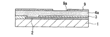
次に、図3に示すように、保護膜3上に突起体4を構成する樹脂、すなわちポジ型レジストとなるアクリル樹脂を、例えば10〜20μm程度に塗布し、さらにプリベークすることによって樹脂層4aを形成する。そして、図4に示すように、樹脂層4a上に、マスク9を所定位置に位置決めしてこれを配置する。マスク9としては、例えばCr等の遮光膜を形成したガラス板からなるもので、形成する半球状の突起体4の平面形状に対応した円形の開口9aを有したものが用いられる。なお、マスク9の位置決めについては、その開口9aが上記突起体4の形成箇所に位置するように行う。
Next, as shown in FIG. 3, a
次いで、このマスク9上に紫外光を照射し、開口9a内に露出する上記樹脂層4aを露光する。ただし、この露光に際しては、その露光条件を調整することにより、現像後に得られる樹脂層4aからなるパターンを、その上面が凸形状の曲面となるパターンにする。
具体的には、樹脂層4aの材質や厚さに対して、標準的な露光量より十分に少ない量で露光する、いわゆるアンダー露光を行う。なお、実際に行う露光(アンダー露光)としては、例えば標準的な露光量の半分程度で行う。
Next, the
Specifically, so-called underexposure is performed in which the material and thickness of the
このようにして、露光を行うと、マスク9の開口9a内に露出する樹脂層4aでは、開口9aの中心から周辺部に行くに連れて漸次露光量が少なくなる。従って、このようにして露光処理を行った後、現像処理を行うと、開口9a内に露出した樹脂層4aにおいても、露光量が少なくなったことで生じた未露光部分が現像され、除去される。すなわち、樹脂層4aは開口9aの中心から周辺部に行くに連れてその表層側の露光の度合いが漸次少なくなることから、この露光の度合いが少なくなって未露光部分となった樹脂が現像・除去される。その結果、図5に示すように、樹脂層4aは上面が凸形状の曲面となるパターン、つまり略截頭角錐状の突起体4となるのである。
When exposure is performed in this manner, the amount of exposure gradually decreases from the center of the
このようにして、樹脂層4aの未露光部分を除去して、突起体4を形成した後、図6に示すように、保護膜3の開口部に露出して形成される電極2及び突起体4の上面を含む基板1の表面全面に、スパッタリング(スパッタ法)によってAu、TiW、Cu、Cr、Ni、Ti、W、NiV、Al、Pd、鉛フリーハンダ等の金属からなる導電材料(パターニングすることにより第1導電層となる)を成膜する。この導電材料層6(導電層)の厚さとしては、例えば200nm程度である。
In this way, after removing the unexposed portion of the
次いで、導電材料層6上の全面にレジストをスピンコート法、ディッピング法、スプレーコート法等によって塗布し、レジスト層を形成する。そして、形成する第1導電層5の平面形状(平面パターン)に対応したマスクを用いてレジスト層に露光処理及び現像処理を施し、これを所定形状にパターニングする。これにより、図7に示すように、形成する第1導電層5のパターン形状に対応したレジストパターン14を形成する。
Next, a resist is applied to the entire surface of the conductive material layer 6 by a spin coating method, a dipping method, a spray coating method, or the like to form a resist layer. Then, the resist layer is subjected to exposure processing and development processing using a mask corresponding to the planar shape (planar pattern) of the first
次いで、上記導電材料層6のレジストパターン14に覆われない部分をエッチングによって除去する。これにより、図8に示すように、保護膜3に形成された開口部を含んだ保護膜3上から突起体4の上面を覆うようにして電極2と電気的に接続される第1導電層5が形成される。なお、ここでのエッチングとしては、例えばプラズマを用いたドライエッチングや、薬液を用いるウエットエッチングなど、任意の手法を採用することができる。
最後に、図9に示すように、レジストパターン14を除去し、さらに必要に応じてダイシングによって個片化することにより、本発明の半導体装置10を得ることができる。
Next, the portion of the conductive material layer 6 not covered with the resist
Finally, as shown in FIG. 9, the
[第2実施形態]
以下に本実施形態について図面を参照して説明する。
上記実施形態では、半導体装置の形成方法において、電極2から突起体4の上面まで引き廻される導電部を、第1導電層5の一層により形成していた。これに対し、本実施形態では、電極2から突起体4の上面まで引き廻される導電部を、第1導電層5と第2導電層7との2層から形成する点において異なる。なお、その他の半導体装置の形成方法は、上記第1実施形態と同様であり、共通の構成要素には同一の符号を付し、詳細な説明は省略する。
[Second Embodiment]
The present embodiment will be described below with reference to the drawings.
In the above embodiment, in the method for forming a semiconductor device, the conductive portion led from the
まず、上記第1実施形態の図2から図6に示す製造工程により、基板1上に電極2と、電極2よりも突出した樹脂からなる突起体4と、電極2に電気的に接続され、かつ突起体4上面を覆う導電材料層6(後述において第1導電層となる層)を形成する。
First, the manufacturing process shown in FIGS. 2 to 6 of the first embodiment is electrically connected to the
次いで、図10に示すように、導電材料層6上の全面にレジストをスピンコート法、ディッピング法、スプレーコート法等によって塗布し、レジスト層を形成する。そして、第2導電層7の平面形状(平面パターン)に対応したマスクを用いてレジスト層に露光処理及び現像処理(フォトリソグラフィー処理)を施し、レジスト層を所定形状にパターニングする。これにより、図10に示すように、形成する第2導電層7のパターンに対応する開口形状を有したレジストパターン11を形成する。
Next, as shown in FIG. 10, a resist is applied to the entire surface of the conductive material layer 6 by a spin coating method, a dipping method, a spray coating method, or the like to form a resist layer. Then, using a mask corresponding to the planar shape (planar pattern) of the second
次いで、図11に示すように、導電材料層6のレジストパターン11に覆われない部分、すなわち露出した導電材料層6をシード層として、電解メッキ処理を施す。電解メッキ処理により、導電材料層6上にAu,Cu等のメッキ層を堆積させ、第2導電層7を形成する。このとき、第2導電層7の膜厚は、第1導電層5よりも厚く、例えば1〜2μm程度に形成する。第2導電層7の膜厚を1μm未満とした場合には、層強度が弱くなり、実装時の加熱加圧処理によって突起体4が変形した際に第1導電層5及び第2導電層7が追従できず、断線等が生じてしまうからである。一方、第2導電層7の膜厚を2μm超とした場合には、層厚が厚くなり膜強度は向上するが、メッキ処理の時間が長くなるとともに、狭ピッチ化が困難となるからである。
Next, as shown in FIG. 11, electrolytic plating is performed using the portion of the conductive material layer 6 that is not covered with the resist
次に、図12に示すように、導電材料層6上に残留したレジストパターン11を除去する。次に、第2導電層7に覆われていない導電材料層6、すなわち非導電部となる部分をエッチング処理により除去する。エッチング処理は、第2導電層7をマスクにして、第2導電層7に覆われない導電材料層6を選択的に除去する。エッチング処理の方法としては、ドライエッチング、又はウエットエッチングのいずれも採用可能である。これにより、第2導電層7と略同形状にパターニングされた第1導電層5が形成される。このようにして、電極2上から突起体4の頂部にまで延びて形成された第1導電層5と第2導電層7との積層構造からなる導電部とを形成する。なお、本実施形態では、突起体4と突起体4上に積層される第1導電層5及び第2導電層7とで外部電極8を形成している。その後、必要に応じてダイシングによって個片化することにより、本発明の半導体装置10を得る。
Next, as shown in FIG. 12, the resist
<電気光学装置>
続いて、上記製造方法により製造された半導体装置10を、例えば、液晶表示装置(電気光学装置)の配線基板上に実装して液晶表示装置を製造する方法について図面を参照して説明する。この実装方法として、COG(Chip On Glass)接続が好適に用いられる。
<Electro-optical device>
Next, a method for manufacturing a liquid crystal display device by mounting the
図13は、COG式液晶表示装置の一例を示した図である。図13に示すように、電気光学装置としての液晶表示装置50は、金属板から成る枠状のシールドケース68と、電気光学パネルとしての液晶パネル52と、液晶駆動用LSI58と、液晶パネル52と液晶駆動用LSI58の能動面に形成されたバンプとをCOG実装方式によって互いに電気的に接続するためのACF(不図示)と、全体の強度を保つための保持部材172とを備えている。
FIG. 13 shows an example of a COG type liquid crystal display device. As shown in FIG. 13, a liquid
さらに、液晶パネル52は、配線基板20と、この基板に対向して配置された対向基板53と備えている。配線基板20は、ガラス基板等から構成され、配線基板20上には、マトリクス状に形成された複数の走査線及びデータ線と、これらに接続されたスイッチング素子(図示省略)と、このスイッチング素子に接続された画素電極(図示省略)と、上記半導体装置10の複数の外部電極8の配置に対応して形成された複数の電極端子22とを備えている。
Further, the
図14は、上記半導体装置10を配線基板20にCOG実装した部分を拡大した断面図である。まず、半導体装置10に形成された外部電極8と配線基板20に形成された電極端子22とを接続させるための接合材24を配線基板20に配置する。この接合材24は、半導体装置10に配置しても良いし、半導体装置10と配線基板20との両方に配置しても良い。また、本実施の形態においては、半導体装置10の外部電極8と配線基板20の電極端子22とを接続する方法として、NCP(Non Conductive Paste)方式を採用している。従って、接合材24としては、絶縁性樹脂であるNCFが用いられる。このNCFは熱硬化性のエポキシ樹脂から構成され、ガラス転移温度としては220℃付近である。
FIG. 14 is an enlarged cross-sectional view of a portion where the
次に、接合材24であるNCPを配置した配線基板20上に、半導体装置10を実装する。半導体装置10の実装は、半導体装置10の外部電極8と配線基板20の電極端子22との位置を合わせを行い、フリップチップボンダにより200℃から260℃の範囲内において半導体基板1と配線基板20とを加熱加圧する。実装温度を上記範囲内とする理由は、実装温度が200℃未満の場合には、半導体装置10の外部電極8を構成する樹脂の弾性力が低下せず、樹脂の形状が変形しないからである。一方、260℃超の場合には、外部電極8を構成する樹脂の弾性力が低下し、樹脂が変形する前に、接合材24であるNCPが硬化してしまい、接続不良が発生してしまうからである。従って、本実施の形態においては、半導体装置10の外部電極8を構成する樹脂のガラス転移温度が上記実装範囲内である約220℃のものを使用して、樹脂の弾性力の低下時に実装が行えるようにしている。
Next, the
図15は、突起体4を構成する樹脂にアクリル樹脂を使用した場合の樹脂の弾性率と実装温度との関係を示した図である。図中のグラフの横軸は実装温度(℃)の変化を示し、縦軸は樹脂の弾性力(Pa)の変化を対数で示している。また、上記測定温度は30℃から開始し、300℃で終了した。なお、昇温速度としては4℃/minである。図15に示すように、実装温度が約170℃付近において、アクリル樹脂の弾性率が低下を開始する。そして、実装温度の上昇とともに、樹脂の弾性率が低下し続けている。実装温度が200℃から260℃の範囲内においては、アクリル樹脂のガラス転移温度が約220℃付近であるため、アクリル樹脂の弾性率が低下している。従って、フリップチップボンダによる加圧に対して、接合材24であるNCPが硬化する前、すなわち実装温度が260℃に達する前に、アクリル樹脂からなる突起体4が変形することになる。
FIG. 15 is a diagram showing the relationship between the elastic modulus of the resin and the mounting temperature when an acrylic resin is used as the resin constituting the
加熱加圧処理は例えば5〜10秒行い、樹脂からなる突起体4を変形させて半導体装置10の外部電極8と配線基板20の電極端子22とを電気的に接続する。そして、上記接合材24であるNCPを硬化させて、この状態を固定、保持させる。このようにして、図13及び14に示すように、半導体装置10を配線基板20にCOG実装させる。
The heat and pressure treatment is performed, for example, for 5 to 10 seconds, and the
このような構成によれば、樹脂のガラス転移温度を含む温度範囲内で加熱加圧処理を施すため、半導体装置10を基板1に実装する温度で、樹脂からなる突起体4の弾性率が低下する。これにより、実装時の加熱加圧処理により、半導体装置10の突起体4からなる外部電極8が変形し、基板1の電極端子22と確実に接続することができる。その結果、導通不良を解消し、接続信頼性の向上を図ることが可能となる。また、NCP方式により接続することができるため、異方性導電粒子を含有する接合材を使用する必要がなく、低コスト化を図ることが可能となる。また、常温での弾性率が高い樹脂を用いて突起体4を製造することが可能となる。その結果、樹脂の選択肢が増えるため、安価な樹脂を使用することができ、低コスト化を図ることが可能となる。さらに、上述したような樹脂を突起体4に使用することにより、実装時に樹脂の弾性率が低下するため、低荷重での実装が可能となる。これにより、半導体装置10のスイッチング素子等が存在する領域上への突起体4の形成が可能となり、半導体装置10上であればスイッチング素子が存在する領域であるか否かにかかわらず形成することが可能となる。さらには、スイッチング素子等が存在する領域上に上記突起体4を形成する場合には、従来、突起体4を形成していた領域を削減することができ、この結果、半導体装置の小型化を図ることが可能となる。
According to such a configuration, since the heat and pressure treatment is performed within the temperature range including the glass transition temperature of the resin, the elastic modulus of the
図16は、上述した液晶表示装置とは、別の構成により製造した液晶表示装置の概略構成を示す斜視図である。図16に示す液晶表示装置は、電気光学パネルとしてのカラーの液晶パネル51と、この液晶パネル51に接続されたCOF(Chip On Film)式の回路基板100とを備えて構成されたものであり、回路基板100は、前記半導体装置の製造方法によって製造された半導体装置101を備えて構成されたものである。このような構成のもとに、回路基板100は本発明の回路基板の一実施形態となっており、また液晶表示装置は本発明の電気光学装置の一実施形態となっている。なお、前記液晶表示装置においては、バックライト等の照明装置やその他の付帯機器が、必要に応じて液晶パネル51に付設されるようになっている。また、回路基板100としては、COF式のものに限定されることなく、COB(Chip On Board)のものを用いることもできる。
また、本発明は、前記COF式のものやCOB式のもの以外にも、表示体パネル(液晶パネル)上に直接ドライバーIC等を実装するCOG(Chip On Glass)式の電気光学装置にも適用可能である。
FIG. 16 is a perspective view showing a schematic configuration of a liquid crystal display device manufactured by a configuration different from the above-described liquid crystal display device. The liquid crystal display device shown in FIG. 16 includes a color
In addition to the COF type and the COB type, the present invention is also applicable to a COG (Chip On Glass) type electro-optical device in which a driver IC or the like is mounted directly on a display panel (liquid crystal panel). Is possible.
なお、電気光学装置としては、液晶表示装置以外にも例えば有機EL表示装置に用いることができる。図17は、本発明による電気光学装置としての有機EL表示装置に設けられる有機ELパネルの断面図である。有機ELパネル(電気光学パネル)30は、基板31上にマトリクス状にTFT(Thin Film Transistor)32を形成し、さらにその上に複数の積層体33を形成して概略構成されたものである。TFT32は、ソース電極、ゲート電極、及びドレイン電極を有したもので、ゲート電極及びソース電極は、例えば図1に示した外部電極8と電気的に接続されている。前記積層体33は、陽極層34、正孔注入層35、発光層36、及び陰極層37を含んで構成されたものである。前記陽極層34は、TFT32のドレイン電極と接続されており、TFT32がオン状態にあるときに電流が、TFT32のソース電極及びドレイン電極を介して陽極層34に供給されるようになっている。
In addition to the liquid crystal display device, the electro-optical device can be used for an organic EL display device, for example. FIG. 17 is a cross-sectional view of an organic EL panel provided in an organic EL display device as an electro-optical device according to the present invention. The organic EL panel (electro-optical panel) 30 is generally configured by forming TFTs (Thin Film Transistors) 32 in a matrix on a
以上の構成の有機ELパネル30において、陽極層34から正孔注入層35を介して発光層36に注入された正孔(ホール)と、陰極層37から発光層36に注入された電子とが発光層36内において再結合して生ずる光は、基板31側から射出される。
In the
次に、本実施の形態の電気光学装置が搭載される電子機器について説明する。以上に説明した電気光学装置としての液晶表示装置、CPU(中央処理装置)等を備えたマザーボード、キーボード、ハードディスク等の電子部品を筐体内に組み込むことで、例えば図18に示すノート型のパーソナルコンピュータ60(電子機器)が製造される。
図18は、本発明の一実施の形態による電子機器としてのノート型コンピュータを示す外観図である。図18において61は筐体であり、62は液晶表示装置(電気光学装置)であり、63はキーボードである。なお、図18においては、液晶表示装置を備えるノート形コンピュータを示しているが、液晶表示装置に代えて有機EL表示装置を備えていても良い。
Next, an electronic apparatus in which the electro-optical device of this embodiment is mounted will be described. By incorporating electronic components such as a liquid crystal display device as an electro-optical device described above, a motherboard having a CPU (central processing unit), a keyboard, a hard disk, and the like into the housing, for example, a notebook personal computer shown in FIG. 60 (electronic equipment) is manufactured.
FIG. 18 is an external view showing a notebook computer as an electronic apparatus according to an embodiment of the present invention. In FIG. 18, 61 is a housing, 62 is a liquid crystal display device (electro-optical device), and 63 is a keyboard. Note that FIG. 18 shows a notebook computer provided with a liquid crystal display device, but an organic EL display device may be provided instead of the liquid crystal display device.
また、上記実施の形態では、電子機器としてノート型コンピュータを例に挙げて説明したが、これらに限らず、携帯電話、液晶プロジェクタ、マルチメディア対応のパーソナルコンピュータ(PC)及びエンジニアリング・ワークステーション(EWS)、ページャ、ワードプロセッサ、テレビ、ビューファインダ型又はモニタ直視型のビデオテープレコーダ、電子手帳、電子卓上計算機、カーナビゲーション装置、POS端末、タッチパネルを備えた装置等の電子機器に適用することが可能である。 In the above embodiment, a notebook computer has been described as an example of an electronic device. However, the present invention is not limited to this, and is not limited thereto. A mobile phone, a liquid crystal projector, a multimedia-compatible personal computer (PC), and an engineering workstation (EWS). ), Pager, word processor, TV, viewfinder type or monitor direct-view type video tape recorder, electronic notebook, electronic desk calculator, car navigation device, POS terminal, touch panel and other electronic devices. is there.
以上、本発明の実施の形態による半導体装置及びその製造方法、電気光学装置、並びに電子機器について説明したが、本発明は上記実施の形態に制限されることなく、本発明の範囲内で自由に変更が可能である。
例えば前述した実施の形態の「半導体素子」を「電子素子」に置き換えて、電子部品を製造することもできる。このような電子素子を使用して製造される電子部品として、例えば、光素子、抵抗器、コンデンサ、コイル、発振器、フィルタ、温度センサ、サーミスタ、バリスタ、ボリューム又はヒューズなどがある。
The semiconductor device and the manufacturing method thereof, the electro-optical device, and the electronic apparatus according to the embodiments of the present invention have been described above. However, the present invention is not limited to the above-described embodiments, and can be freely made within the scope of the present invention. It can be changed.
For example, an electronic component can be manufactured by replacing the “semiconductor element” in the above-described embodiment with an “electronic element”. Examples of electronic components manufactured using such electronic elements include optical elements, resistors, capacitors, coils, oscillators, filters, temperature sensors, thermistors, varistors, volumes or fuses.
1…基板、 2…電極、 3…保護膜、 4…突起体(凸部)、 4a…樹脂層、 5…第1導電層(導電部)、 6…導電材料層(導電層)、 7…第2導電層(導電部)、
8…外部電極、 10…半導体装置、 20…配線基板、 22…電極端子、 24…接合材、 62…液晶表示装置(電気光学装置)
DESCRIPTION OF
DESCRIPTION OF
Claims (11)
前記樹脂のガラス転移温度を含む温度範囲内で加熱加圧処理を施すことにより前記半導体装置を実装することを特徴とする半導体装置の実装方法。 A semiconductor device comprising: an electrode; a convex portion protruding from the electrode and formed of a resin; and a conductive portion electrically connected to the electrode and reaching the upper surface of the convex portion. A mounting method of a semiconductor device to be mounted on a substrate via
A method for mounting a semiconductor device, wherein the semiconductor device is mounted by performing a heat and pressure treatment within a temperature range including a glass transition temperature of the resin.
スパッタ法により導電層を形成し、前記導電層をパターニングして前記電極に接続され
、かつ前記凸部の上面に到る第1導電層を形成することを特徴とする請求項1乃至請求項
5のいずれか1項に記載の半導体装置の製造方法。 In the step of forming the conductive portion,
6. A conductive layer is formed by a sputtering method, and the conductive layer is patterned to form a first conductive layer connected to the electrode and reaching the upper surface of the convex portion. The method for manufacturing a semiconductor device according to any one of the above.
前記導電層上にメッキ法により第2導電層を形成し、前記第2導電層に覆われていない導電層を除去して第1導電層を形成することを特徴とする請求項6に記載の半導体装置の製造方法。 In the step of forming the conductive portion,
The second conductive layer is formed on the conductive layer by a plating method, and the first conductive layer is formed by removing the conductive layer not covered with the second conductive layer. A method for manufacturing a semiconductor device.
Priority Applications (5)
| Application Number | Priority Date | Filing Date | Title |
|---|---|---|---|
| JP2005008686A JP2005340761A (en) | 2004-04-27 | 2005-01-17 | Semiconductor device mounting method, circuit board, electro-optical device, and electronic apparatus |
| TW094109793A TWI257650B (en) | 2004-04-27 | 2005-03-29 | Method for mounting semiconductor device, as well as circuit board, electrooptic device, and electronic device |
| US11/103,942 US20050236104A1 (en) | 2004-04-27 | 2005-04-12 | Method for mounting semiconductor device, as well as circuit board, electrooptic device, and electronic device |
| KR1020050034362A KR100643984B1 (en) | 2004-04-27 | 2005-04-26 | Method for mounting semiconductor device, circuit board, electrooptic device, and electronic device |
| US12/474,329 US8142602B2 (en) | 2004-04-27 | 2009-05-29 | Method for mounting semiconductor device |
Applications Claiming Priority (2)
| Application Number | Priority Date | Filing Date | Title |
|---|---|---|---|
| JP2004130866 | 2004-04-27 | ||
| JP2005008686A JP2005340761A (en) | 2004-04-27 | 2005-01-17 | Semiconductor device mounting method, circuit board, electro-optical device, and electronic apparatus |
Publications (1)
| Publication Number | Publication Date |
|---|---|
| JP2005340761A true JP2005340761A (en) | 2005-12-08 |
Family
ID=35135262
Family Applications (1)
| Application Number | Title | Priority Date | Filing Date |
|---|---|---|---|
| JP2005008686A Pending JP2005340761A (en) | 2004-04-27 | 2005-01-17 | Semiconductor device mounting method, circuit board, electro-optical device, and electronic apparatus |
Country Status (4)
| Country | Link |
|---|---|
| US (2) | US20050236104A1 (en) |
| JP (1) | JP2005340761A (en) |
| KR (1) | KR100643984B1 (en) |
| TW (1) | TWI257650B (en) |
Cited By (9)
| Publication number | Priority date | Publication date | Assignee | Title |
|---|---|---|---|---|
| US7246432B2 (en) | 2005-06-28 | 2007-07-24 | Seiko Epson Corporation | Method of manufacturing semiconductor device |
| JP2007300052A (en) * | 2006-04-28 | 2007-11-15 | Chukaminkoku Taiwan Hakumaku Denshotai Ekisho Keijiki Sangyo Kyokai | Flip chip mounting parts and manufacturing method thereof |
| JP2008186836A (en) * | 2007-01-26 | 2008-08-14 | Seiko Epson Corp | SEMICONDUCTOR DEVICE, ITS MANUFACTURING METHOD, AND ELECTRONIC DEVICE MANUFACTURING METHOD |
| JP2009049156A (en) * | 2007-08-20 | 2009-03-05 | Seiko Epson Corp | Semiconductor device and electronic device |
| JP2009164493A (en) * | 2008-01-09 | 2009-07-23 | Shinko Electric Ind Co Ltd | WIRING BOARD AND ITS MANUFACTURING METHOD, ELECTRONIC COMPONENT DEVICE AND ITS MANUFACTURING METHOD |
| US7629671B2 (en) | 2005-07-06 | 2009-12-08 | Seiko Epson Corporation | Semiconductor device having a resin protrusion with a depression and method manufacturing the same |
| US7671476B2 (en) | 2005-06-29 | 2010-03-02 | Seiko Epson Corporation | Semiconductor device and method of manufacturing the same |
| US8178968B2 (en) | 2007-11-02 | 2012-05-15 | Seiko Epson Corporation | Electronic component |
| KR20230144929A (en) * | 2022-04-07 | 2023-10-17 | 칩본드 테크놀러지 코포레이션 | Flip chip bonding method and chip used therein |
Families Citing this family (18)
| Publication number | Priority date | Publication date | Assignee | Title |
|---|---|---|---|---|
| JP4665631B2 (en) * | 2005-07-07 | 2011-04-06 | セイコーエプソン株式会社 | Electronic substrate, method for manufacturing the same, method for manufacturing electro-optical device, and method for manufacturing electronic apparatus |
| JP4419926B2 (en) * | 2005-07-14 | 2010-02-24 | セイコーエプソン株式会社 | Semiconductor device |
| JP4645832B2 (en) * | 2005-08-02 | 2011-03-09 | セイコーエプソン株式会社 | Semiconductor device and manufacturing method thereof |
| US20070267737A1 (en) * | 2006-05-17 | 2007-11-22 | Taiwan Semiconductor Manufacturing Co., Ltd. | Packaged devices and methods for forming packaged devices |
| CN101611490B (en) * | 2007-02-16 | 2011-07-27 | 住友电木株式会社 | Circuit board manufacturing method, semiconductor manufacturing apparatus, circuit board and semiconductor device |
| JP4548459B2 (en) | 2007-08-21 | 2010-09-22 | セイコーエプソン株式会社 | Electronic component mounting structure |
| TWI377632B (en) * | 2008-03-27 | 2012-11-21 | Taiwan Tft Lcd Ass | Contact structure and forming method thereof and connecting structure thereof |
| JP5419226B2 (en) | 2010-07-29 | 2014-02-19 | 日東電工株式会社 | Flip chip type film for semiconductor back surface and use thereof |
| ITTO20130307A1 (en) | 2013-04-17 | 2014-10-18 | Itt Italia Srl | METHOD TO REALIZE A BRAKE ELEMENT, IN PARTICULAR A BRAKE PAD, SENSORIZED, SENSORED BRAKE PAD, VEHICLE BRAKE SYSTEM AND ASSOCIATED METHOD |
| US9939035B2 (en) | 2015-05-28 | 2018-04-10 | Itt Italia S.R.L. | Smart braking devices, systems, and methods |
| ITUB20153706A1 (en) | 2015-09-17 | 2017-03-17 | Itt Italia Srl | BRAKING DEVICE FOR HEAVY VEHICLE AND METHOD OF PREVENTING BRAKE OVERHEATING IN A HEAVY VEHICLE |
| ITUB20153709A1 (en) | 2015-09-17 | 2017-03-17 | Itt Italia Srl | DATA ANALYSIS AND MANAGEMENT DEVICE GENERATED BY A SENSORIZED BRAKE SYSTEM FOR VEHICLES |
| ITUA20161336A1 (en) | 2016-03-03 | 2017-09-03 | Itt Italia Srl | DEVICE AND METHOD FOR IMPROVING THE PERFORMANCE OF A VEHICLE ANTI-LOCK AND ANTI-SLIP SYSTEM |
| IT201600077944A1 (en) | 2016-07-25 | 2018-01-25 | Itt Italia Srl | DEVICE FOR DETECTION OF RESIDUAL BRAKING TORQUE IN A VEHICLE EQUIPPED WITH DISC BRAKES |
| JP2019134019A (en) * | 2018-01-30 | 2019-08-08 | セイコーエプソン株式会社 | Light-emitting device |
| KR20190125888A (en) * | 2018-04-30 | 2019-11-07 | 에스케이하이닉스 주식회사 | Method of stacking multiple semiconductor dies |
| IT201900015839A1 (en) | 2019-09-06 | 2021-03-06 | Itt Italia Srl | BRAKE PAD FOR VEHICLES AND ITS PRODUCTION PROCESS |
| US20240241003A1 (en) | 2021-05-25 | 2024-07-18 | Itt Italia S.R.L. | A method and a device for estimating residual torque between the braked and braking elements of a vehicle |
Citations (6)
| Publication number | Priority date | Publication date | Assignee | Title |
|---|---|---|---|---|
| JPH08195397A (en) * | 1995-01-19 | 1996-07-30 | Fuji Electric Co Ltd | Semiconductor device with bump and manufacturing method thereof |
| JPH1167776A (en) * | 1997-08-21 | 1999-03-09 | Citizen Watch Co Ltd | Protruded electrode and its manufacture |
| JP2001077516A (en) * | 1999-07-05 | 2001-03-23 | Matsushita Electric Ind Co Ltd | Electronic component device, method of manufacturing the same, and circuit board |
| JP2001110831A (en) * | 1999-10-07 | 2001-04-20 | Seiko Epson Corp | External connection projection and method of forming the same, semiconductor chip, circuit board, and electronic device |
| JP2001144141A (en) * | 1999-11-15 | 2001-05-25 | Matsushita Electric Works Ltd | Semiconductor chip mounting method |
| JP2002151533A (en) * | 2000-11-08 | 2002-05-24 | Citizen Watch Co Ltd | Semiconductor device and manufacturing method thereof |
Family Cites Families (15)
| Publication number | Priority date | Publication date | Assignee | Title |
|---|---|---|---|---|
| US4813129A (en) | 1987-06-19 | 1989-03-21 | Hewlett-Packard Company | Interconnect structure for PC boards and integrated circuits |
| JPH02272737A (en) | 1989-04-14 | 1990-11-07 | Citizen Watch Co Ltd | Projecting electrode structure of semiconductor and formation of projecting electrode |
| JPH0396921A (en) | 1989-09-11 | 1991-04-22 | Ricoh Co Ltd | Liquid crystal display device |
| JPH06302606A (en) | 1993-04-16 | 1994-10-28 | Citizen Watch Co Ltd | Method of forming bump electrode |
| US5478913A (en) * | 1993-12-22 | 1995-12-26 | E. I. Du Pont De Nemours And Company | Melt-processible polyimides with high Tg |
| US5508228A (en) * | 1994-02-14 | 1996-04-16 | Microelectronics And Computer Technology Corporation | Compliant electrically connective bumps for an adhesive flip chip integrated circuit device and methods for forming same |
| US5393697A (en) * | 1994-05-06 | 1995-02-28 | Industrial Technology Research Institute | Composite bump structure and methods of fabrication |
| US5427382A (en) * | 1994-05-09 | 1995-06-27 | Pate; Elvis O. | Repair kit for three-dimensional animal targets |
| US5578527A (en) * | 1995-06-23 | 1996-11-26 | Industrial Technology Research Institute | Connection construction and method of manufacturing the same |
| TW324847B (en) * | 1996-12-13 | 1998-01-11 | Ind Tech Res Inst | The structure of composite bump |
| US5783465A (en) * | 1997-04-03 | 1998-07-21 | Lucent Technologies Inc. | Compliant bump technology |
| JP3405269B2 (en) * | 1999-04-26 | 2003-05-12 | ソニーケミカル株式会社 | Implementation method |
| US6537854B1 (en) * | 1999-05-24 | 2003-03-25 | Industrial Technology Research Institute | Method for bonding IC chips having multi-layered bumps with corrugated surfaces and devices formed |
| JP3839323B2 (en) * | 2001-04-06 | 2006-11-01 | 株式会社ルネサステクノロジ | Manufacturing method of semiconductor device |
| JP3969295B2 (en) | 2002-12-02 | 2007-09-05 | セイコーエプソン株式会社 | SEMICONDUCTOR DEVICE, ITS MANUFACTURING METHOD, CIRCUIT BOARD, ELECTRO-OPTICAL DEVICE, AND ELECTRONIC DEVICE |
-
2005
- 2005-01-17 JP JP2005008686A patent/JP2005340761A/en active Pending
- 2005-03-29 TW TW094109793A patent/TWI257650B/en not_active IP Right Cessation
- 2005-04-12 US US11/103,942 patent/US20050236104A1/en not_active Abandoned
- 2005-04-26 KR KR1020050034362A patent/KR100643984B1/en not_active Expired - Fee Related
-
2009
- 2009-05-29 US US12/474,329 patent/US8142602B2/en not_active Expired - Fee Related
Patent Citations (6)
| Publication number | Priority date | Publication date | Assignee | Title |
|---|---|---|---|---|
| JPH08195397A (en) * | 1995-01-19 | 1996-07-30 | Fuji Electric Co Ltd | Semiconductor device with bump and manufacturing method thereof |
| JPH1167776A (en) * | 1997-08-21 | 1999-03-09 | Citizen Watch Co Ltd | Protruded electrode and its manufacture |
| JP2001077516A (en) * | 1999-07-05 | 2001-03-23 | Matsushita Electric Ind Co Ltd | Electronic component device, method of manufacturing the same, and circuit board |
| JP2001110831A (en) * | 1999-10-07 | 2001-04-20 | Seiko Epson Corp | External connection projection and method of forming the same, semiconductor chip, circuit board, and electronic device |
| JP2001144141A (en) * | 1999-11-15 | 2001-05-25 | Matsushita Electric Works Ltd | Semiconductor chip mounting method |
| JP2002151533A (en) * | 2000-11-08 | 2002-05-24 | Citizen Watch Co Ltd | Semiconductor device and manufacturing method thereof |
Cited By (13)
| Publication number | Priority date | Publication date | Assignee | Title |
|---|---|---|---|---|
| US7246432B2 (en) | 2005-06-28 | 2007-07-24 | Seiko Epson Corporation | Method of manufacturing semiconductor device |
| US7825518B2 (en) | 2005-06-29 | 2010-11-02 | Seiko Epson Corporation | Semiconductor device and method of manufacturing the same |
| US7936073B2 (en) | 2005-06-29 | 2011-05-03 | Seiko Epson Corporation | Semiconductor device and method of manufacturing the same |
| US7671476B2 (en) | 2005-06-29 | 2010-03-02 | Seiko Epson Corporation | Semiconductor device and method of manufacturing the same |
| US7629671B2 (en) | 2005-07-06 | 2009-12-08 | Seiko Epson Corporation | Semiconductor device having a resin protrusion with a depression and method manufacturing the same |
| JP2007300052A (en) * | 2006-04-28 | 2007-11-15 | Chukaminkoku Taiwan Hakumaku Denshotai Ekisho Keijiki Sangyo Kyokai | Flip chip mounting parts and manufacturing method thereof |
| JP2008186836A (en) * | 2007-01-26 | 2008-08-14 | Seiko Epson Corp | SEMICONDUCTOR DEVICE, ITS MANUFACTURING METHOD, AND ELECTRONIC DEVICE MANUFACTURING METHOD |
| JP2009049156A (en) * | 2007-08-20 | 2009-03-05 | Seiko Epson Corp | Semiconductor device and electronic device |
| US8178968B2 (en) | 2007-11-02 | 2012-05-15 | Seiko Epson Corporation | Electronic component |
| JP2009164493A (en) * | 2008-01-09 | 2009-07-23 | Shinko Electric Ind Co Ltd | WIRING BOARD AND ITS MANUFACTURING METHOD, ELECTRONIC COMPONENT DEVICE AND ITS MANUFACTURING METHOD |
| US8062927B2 (en) | 2008-01-09 | 2011-11-22 | Shinko Electric Industries Co., Ltd. | Wiring board and method of manufacturing the same, and electronic component device using the wiring board and method of manufacturing the same |
| KR20230144929A (en) * | 2022-04-07 | 2023-10-17 | 칩본드 테크놀러지 코포레이션 | Flip chip bonding method and chip used therein |
| KR102809068B1 (en) * | 2022-04-07 | 2025-05-16 | 칩본드 테크놀러지 코포레이션 | Flip chip bonding method and chip used therein |
Also Published As
| Publication number | Publication date |
|---|---|
| US8142602B2 (en) | 2012-03-27 |
| KR100643984B1 (en) | 2006-11-10 |
| TW200537582A (en) | 2005-11-16 |
| US20050236104A1 (en) | 2005-10-27 |
| TWI257650B (en) | 2006-07-01 |
| KR20060046693A (en) | 2006-05-17 |
| US20090242122A1 (en) | 2009-10-01 |
Similar Documents
| Publication | Publication Date | Title |
|---|---|---|
| KR100643984B1 (en) | Method for mounting semiconductor device, circuit board, electrooptic device, and electronic device | |
| JP3969295B2 (en) | SEMICONDUCTOR DEVICE, ITS MANUFACTURING METHOD, CIRCUIT BOARD, ELECTRO-OPTICAL DEVICE, AND ELECTRONIC DEVICE | |
| KR100546346B1 (en) | Rewiring bump formation method and semiconductor chip and mounting structure using same | |
| JP4218622B2 (en) | Manufacturing method of semiconductor device | |
| JP4784304B2 (en) | Electronic component, method for manufacturing electronic component, circuit board, and electronic device | |
| JP3938128B2 (en) | SEMICONDUCTOR DEVICE AND ITS MANUFACTURING METHOD, CIRCUIT BOARD, ELECTRO-OPTICAL DEVICE, AND ELECTRONIC DEVICE | |
| JP4151634B2 (en) | SEMICONDUCTOR DEVICE AND ITS MANUFACTURING METHOD, CIRCUIT BOARD, ELECTRO-OPTICAL DEVICE, AND ELECTRONIC DEVICE | |
| JP4419926B2 (en) | Semiconductor device | |
| JP4329661B2 (en) | Semiconductor device, circuit board, and electro-optical device | |
| CN100468668C (en) | Semiconductor device mounting method, circuit substrate, electro-optical device, and electronic instrument | |
| JP4826852B2 (en) | Semiconductor device, electro-optical device and electronic apparatus | |
| JP2007042777A (en) | SEMICONDUCTOR DEVICE AND ITS MANUFACTURING METHOD, CIRCUIT BOARD, ELECTRO-OPTICAL DEVICE, AND ELECTRONIC DEVICE | |
| JP4862390B2 (en) | Manufacturing method of electronic substrate | |
| JP5088309B2 (en) | Electronic substrate, electro-optical device, and electronic apparatus | |
| CN100521151C (en) | Electronic substrate and its manufacturing method, electro-optical device manufacturing method, and electronic apparatus manufacturing method |
Legal Events
| Date | Code | Title | Description |
|---|---|---|---|
| RD04 | Notification of resignation of power of attorney |
Free format text: JAPANESE INTERMEDIATE CODE: A7424 Effective date: 20070403 |
|
| A621 | Written request for application examination |
Free format text: JAPANESE INTERMEDIATE CODE: A621 Effective date: 20080116 |
|
| A977 | Report on retrieval |
Free format text: JAPANESE INTERMEDIATE CODE: A971007 Effective date: 20100215 |
|
| A131 | Notification of reasons for refusal |
Free format text: JAPANESE INTERMEDIATE CODE: A131 Effective date: 20100223 |
|
| A521 | Request for written amendment filed |
Free format text: JAPANESE INTERMEDIATE CODE: A523 Effective date: 20100423 |
|
| A131 | Notification of reasons for refusal |
Free format text: JAPANESE INTERMEDIATE CODE: A131 Effective date: 20100525 |
|
| A521 | Request for written amendment filed |
Free format text: JAPANESE INTERMEDIATE CODE: A523 Effective date: 20100723 |
|
| RD03 | Notification of appointment of power of attorney |
Free format text: JAPANESE INTERMEDIATE CODE: A7423 Effective date: 20100723 |
|
| A521 | Request for written amendment filed |
Free format text: JAPANESE INTERMEDIATE CODE: A821 Effective date: 20100726 |
|
| A02 | Decision of refusal |
Free format text: JAPANESE INTERMEDIATE CODE: A02 Effective date: 20100824 |