JP2005302799A - Multilayer printed wiring board - Google Patents
Multilayer printed wiring board Download PDFInfo
- Publication number
- JP2005302799A JP2005302799A JP2004112747A JP2004112747A JP2005302799A JP 2005302799 A JP2005302799 A JP 2005302799A JP 2004112747 A JP2004112747 A JP 2004112747A JP 2004112747 A JP2004112747 A JP 2004112747A JP 2005302799 A JP2005302799 A JP 2005302799A
- Authority
- JP
- Japan
- Prior art keywords
- wiring board
- printed wiring
- layer
- signal
- multilayer printed
- Prior art date
- Legal status (The legal status is an assumption and is not a legal conclusion. Google has not performed a legal analysis and makes no representation as to the accuracy of the status listed.)
- Withdrawn
Links
Images


Landscapes
- Production Of Multi-Layered Print Wiring Board (AREA)
- Shielding Devices Or Components To Electric Or Magnetic Fields (AREA)
Abstract
【課題】 多層プリント配線板において、内層配線の電磁雑音の放射を抑圧すると共に、外部もしくは、他の配線からの誘導による電磁雑音の影響を大幅に低減する。
【解決手段】 多層プリント配線板において、内層に配置された信号線の上下の層にグランドもしくは、電源電位に固定した配線を配置し、さらに信号線と同層の両側もしくは、片側にグランドもしくは電源電位に固定された、シールド用ストリップラインもしくは、スルーホールもしくはバイアホールを配置する。
【選択図】 図1
PROBLEM TO BE SOLVED: To suppress the radiation of electromagnetic noise of an inner layer wiring in a multilayer printed wiring board and greatly reduce the influence of electromagnetic noise due to induction from the outside or other wiring.
In a multilayer printed wiring board, ground or wiring fixed to a power supply potential is arranged on the upper and lower layers of a signal line arranged in an inner layer, and further, ground or power supply on both sides or one side of the same layer as the signal line. A shield strip line, a through hole or a via hole fixed at a potential is arranged.
[Selection] Figure 1
Description
本発明は電磁環境適合性(EMC)の高い多層プリント配線板に関する。 The present invention relates to a multilayer printed wiring board having high electromagnetic compatibility (EMC).
電子機器がその意図された電磁環境の中で、機能劣化や損害を与えたり受けたりすることなく共存できるようにさまざまなEMC対策が行われている。 Various EMC countermeasures have been taken so that electronic devices can coexist in the intended electromagnetic environment without causing functional degradation or damage.
最も一般的な対策として、プリント配線板の層構成の変更と絶縁体厚の低減が行われるようになってきた。 As the most general countermeasure, the layer configuration of the printed wiring board is changed and the insulator thickness is reduced.
パソコンのメインボードなどに数多く使われている4層プリント配線板の例を挙げ説明する。 An example of a four-layer printed wiring board that is often used for a main board of a personal computer will be described.
図8は4層のプリント配線板の外形形状を、図9には絶縁体を取り除いた透視図を示している。 FIG. 8 shows the outer shape of a four-layer printed wiring board, and FIG. 9 shows a perspective view with the insulator removed.
1は第1層、2は第2層、3は第3層、4は第4層を示し、各配線層は5,6,7の絶縁層で絶縁されている。配線層の厚さは10μmから40μm、絶縁体層の厚みは100μmから200μm程度である。
4層基板の場合、1層と4層の面に信号層を配置し、内層の2層を接地層と電源層としていた。このためプリント配線板の表面層から電磁雑音が放射されていた。 In the case of a four-layer substrate, signal layers are arranged on the first and fourth layers, and two inner layers are used as a ground layer and a power supply layer. For this reason, electromagnetic noise was radiated from the surface layer of the printed wiring board.
そこで、プリント配線板における放射電磁雑音特性の向上の為の対策として、プリント配線板の1層と4層の面をグランド層もしくは電源層にして、信号配線を2、3層で行うことによって、信号配線から発生した電磁ノイズを内部に閉じ込める層構成。 Therefore, as a measure for improving the radiated electromagnetic noise characteristics in the printed wiring board, the surface of the 1st and 4th layers of the printed wiring board is a ground layer or a power supply layer, and signal wiring is performed in 2 or 3 layers, Layer structure that confines electromagnetic noise generated from signal wiring inside.
信号線とグランド層によって構成される電流のループ面積を小さくし、放射雑音の電界強度を低減させるため、5,6,7の絶縁層の厚みを低減させる。
In order to reduce the loop area of the current formed by the signal line and the ground layer and reduce the electric field strength of the radiation noise, the thicknesses of the
等の方法が採用されてきた。 Etc. have been adopted.
例えば、先行技術としては、特開平8−148832がある。
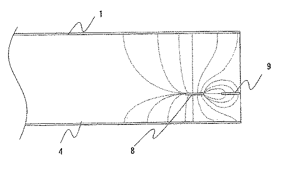
図10にプリント配線板の1層と4層の面をグランド層にして、プリント配線板の3層の信号配線を基板のエッジに配線した場合に発生する電気力線を示す。同図において8は信号配線、11は電気力線を示す。 FIG. 10 shows lines of electric force generated when the first and fourth layers of the printed wiring board are ground layers and the three-layer signal wiring of the printed wiring board is wired to the edge of the substrate. In the figure, 8 is a signal wiring, and 11 is a line of electric force.
プリント配線板の表と裏をグランド電源層で覆った場合、基板の表裏方向からの放射電磁雑音は大幅に低減させることが可能であるが、プリント配線板のエッジ部に信号配線を配置したような場合には、高周波的には開口部がスロットアンテナを形成する。したがって、基板の端面方向からの放射電磁雑音が問題となる。 When the front and back of the printed wiring board are covered with the ground power supply layer, the radiated electromagnetic noise from the front and back of the board can be greatly reduced, but it seems that the signal wiring is arranged at the edge of the printed wiring board. In such a case, the opening forms a slot antenna in terms of high frequency. Therefore, radiated electromagnetic noise from the end face direction of the substrate becomes a problem.
図11に信号配線の配置をプリント配線板のエッジから大きく内側にした場合の電気力線の様子を示す。信号配線8から発生した電気力線のほとんどがプリント配線板の中で閉じ込められていることが分かる。
FIG. 11 shows the lines of electric lines of force when the signal wiring is placed largely inside from the edge of the printed wiring board. It can be seen that most of the lines of electric force generated from the
一般的にこのように高速信号を内層に配線する場合には、基板のグランドもしくは電源層のエッジから、絶縁層の厚みの20倍から100倍の距離を置いて配線することによって多層基板の外側に漏れ出す電気力線を減少させるこことができる。したがって、放射雑音がほとんど放射されないプリント配線板が実現可能である。しかし、多層基板の層間の絶縁層厚は100〜200μm程度ある為、基板の内層周辺部は先のルールを適用すると、信号配線の外側に2〜20mm程度の配線禁止領域が発生してしまう。これは特に小型化を要求される機器のプリント配線板設計時の問題点となっていた。 In general, when wiring a high-speed signal on the inner layer as described above, the wiring is placed at a distance of 20 to 100 times the thickness of the insulating layer from the ground of the substrate or the edge of the power supply layer. It is possible to reduce the electric field lines leaking into the screen. Therefore, it is possible to realize a printed wiring board that hardly emits radiation noise. However, since the insulating layer thickness between the layers of the multilayer substrate is about 100 to 200 μm, if the previous rule is applied to the inner layer peripheral portion of the substrate, a wiring prohibited region of about 2 to 20 mm is generated outside the signal wiring. This has been a problem at the time of designing a printed wiring board for a device that is particularly required to be downsized.
また、放射電磁雑音の強度は周波数の2乗と電流と電流のループ面積に比例する。したがって、プリント配線板の絶縁層の厚みの低減は電流ループ面積を小さくすることから放射電磁雑音の低減の為には非常に有効な対策である。 The intensity of radiated electromagnetic noise is proportional to the square of the frequency and the current and current loop area. Therefore, reducing the thickness of the insulating layer of the printed wiring board is a very effective measure for reducing radiated electromagnetic noise because the current loop area is reduced.
しかし、プリント配線板絶縁層の厚みを低減させた場合、プリント配線板の厚さが薄くなり、剛性が低くなる。このため、プリント配線板の配線の断線、基板の割れ等も問題となってきている。 However, when the thickness of the printed wiring board insulating layer is reduced, the thickness of the printed wiring board becomes thin and the rigidity becomes low. For this reason, the disconnection of the wiring of a printed wiring board, the crack of a board | substrate, etc. have also become a problem.
本発明の目的は、剛性が高く、サイズが小さく、放射電磁雑音を大幅に低減させるプリント配線板を提供することにある。 An object of the present invention is to provide a printed wiring board having high rigidity, small size, and greatly reducing radiated electromagnetic noise.
多層プリント配線板において内層に配置された信号線の上下の層にグランドもしくは電源電位に固定した配線を配置し、さらに信号線と同層の両側もしくは片側にグランドもしくは電源電位に接続されたシールド用ストリップラインもしくはスルーホール、もしくはバイアホールを配置したことによって電磁雑音の放射を防止する機能を備えた事を特徴とするものである。 For shields in which wiring fixed to ground or power supply potential is placed on the upper and lower layers of signal lines placed on the inner layer of a multilayer printed wiring board, and also connected to ground or power supply potential on both sides or one side of the same layer as the signal lines It is characterized in that it has a function of preventing the emission of electromagnetic noise by arranging strip lines, through holes, or via holes.
また、このようにシールド用ストリップラインもしくはスルーホール、もしくはバイアホールを備えることによって外部もしくはプリント配線板内の他の配線からの誘導による電磁雑音の影響も大幅に低減することが可能となる。 Further, by providing the shielding strip line, through hole, or via hole in this way, it is possible to greatly reduce the influence of electromagnetic noise due to induction from the outside or other wiring in the printed wiring board.
以上説明したように本発明によれば、多層プリント配線板において内層に配置された信号線の上下の層にグランドもしくは電源電位に固定した配線を配置し、さらに信号線と同層の両側もしくは片側にグランドもしくは電源電位に接続されたシールド用ストリップラインを配置することによって電磁雑音の放射を防止できる。 As described above, according to the present invention, in the multilayer printed wiring board, wiring fixed to the ground or the power supply potential is disposed on the upper and lower layers of the signal line disposed on the inner layer, and further, both sides or one side of the same layer as the signal line. Electromagnetic noise radiation can be prevented by arranging a shield strip line connected to the ground or power supply potential.
また、このようにシールド電極を備えることによって外部もしくはプリント配線板内の他の配線からの誘導による電磁雑音の影響を大幅に低減することが可能である。 Further, by providing the shield electrode in this way, it is possible to greatly reduce the influence of electromagnetic noise caused by induction from the outside or other wiring in the printed wiring board.
これらの効果を、プリント配線板の厚みや、サイズの大幅な変更を伴わずに実現できる。さらに、導電性ペースト等の利用によってより完全なシールドが実現できる。 These effects can be realized without significant changes in the thickness and size of the printed wiring board. Furthermore, a more complete shield can be realized by using a conductive paste or the like.
以下、本発明の実施の形態について図面を用いて説明する。 Hereinafter, embodiments of the present invention will be described with reference to the drawings.
図1は、本発明の実施の形態に係る多層プリント配線板の透視図である。同図において1は第1層、2は第2層、8および9は第3層、4は第4層の導電層であり、8は信号配線、9はシールド配線、12はシールド配線の電位をグランドに固定する為のスルーホールを示す。 FIG. 1 is a perspective view of a multilayer printed wiring board according to an embodiment of the present invention. In the figure, 1 is the first layer, 2 is the second layer, 8 and 9 are the third layer, 4 is the fourth conductive layer, 8 is the signal wiring, 9 is the shield wiring, and 12 is the potential of the shielding wiring. The through-hole for fixing to the ground is shown.
図2に図1の構成において、信号配線8から発生する電気力線の様子を示す。信号配線がプリント配線板のエッジ付近に配置されているのにもかかわらず、信号配線から発生した電気力線はシールド配線9および第1層および第4層のグランド層によってプリント配線板の中に閉じ込められていることが分かる。
FIG. 2 shows a state of electric lines of force generated from the
一般に信号配線を並行して配置すると、信号配線の特性インピーダンスの変化があるが、本実施例において、配線幅をWとするとシールド配線との間隔を2W取ることによって、信号配線のインピーダンスに与える影響を5%程度に低減できる。 Generally, when signal wirings are arranged in parallel, there is a change in the characteristic impedance of the signal wirings. In this embodiment, if the wiring width is W, the influence on the impedance of the signal wirings by taking 2 W from the shield wiring. Can be reduced to about 5%.
したがって信号配線幅が0.15mmの場合は、信号配線の片側に必要な領域は0.45mm程度となり、小型のプリント配線板で信号配線の定数を変更することなしに、放射電磁雑音を大幅に低減させることが可能となる。 Therefore, when the signal wiring width is 0.15 mm, the required area on one side of the signal wiring is about 0.45 mm, and the radiated electromagnetic noise is greatly reduced without changing the signal wiring constants with a small printed wiring board. It can be reduced.
また、信号配線に流れる信号の高調波とによってシールド配線が共振することを防止する為には、図1のスルーホールの間隔Tpは、信号配線に伝送される信号の最高高調波周波数の波長の1/2以下でなければならない。したがって下記に示す関係式が成り立つ。 In order to prevent the shield wiring from resonating with the harmonics of the signal flowing in the signal wiring, the interval T p between the through holes in FIG. 1 is the wavelength of the highest harmonic frequency of the signal transmitted to the signal wiring. Must be less than half of Therefore, the following relational expression holds.
λ:最大高調波の波長
εr:プリント配線板の比誘電率
C:3×10⁸(m/s)
ここで、100MHzのクロックを信号配線に伝送した場合のスルーホールの間隔を求めてみる。
λ: wavelength of maximum harmonic ε r : relative dielectric constant of printed wiring board C: 3 × 10 8 (m / s)
Here, an interval between through holes when a 100 MHz clock is transmitted to the signal wiring is obtained.
一般的に矩形波には3〜10倍程度の高調波成分が含まれる必要がある為
fm=1GHzとして計算すると、
必要なスルーホールの最大ピッチは64mmとなる。
In general, a rectangular wave needs to contain a harmonic component of about 3 to 10 times, so when calculating as f m = 1 GHz,
The maximum pitch of the necessary through holes is 64 mm.
以下に本発明による第2の実施例を図7を用いて説明する。 A second embodiment according to the present invention will be described below with reference to FIG.
図3は、本発明の第2の実施の形態に係る多層プリント配線板の透視図である。同図において1は第1層、2は第2層、8は第3層、4は第4層の導電層であり、8は信号配線、12はシールド配線の代替のスルーホールを示す。 FIG. 3 is a perspective view of a multilayer printed wiring board according to the second embodiment of the present invention. In the figure, 1 is the first layer, 2 is the second layer, 8 is the third layer, 4 is the fourth conductive layer, 8 is the signal wiring, and 12 is an alternative through hole for the shield wiring.
図4に図3の構成において、信号配線8から発生する電気力線の様子をプリント配線板の厚み方向から見た図を示す。信号配線から発生した電気力線はスルーホール12プリント配線板の中に閉じ込められていることが分かる。
FIG. 4 shows a view of the electric lines of force generated from the
プリント配線板の厚みは信号配線に伝送される信号の最高高調波周波数の波長に対して十分小さいので、スルーホールの間隔Tpを、信号配線に伝送される信号の最高高調波周波数の波長の1/2以下にすることによって、最高高調波周波数以下の周波数の信号を遮断することができる。したがって下記に示す関係式が成り立つ。 Since the thickness of the printed wiring board is sufficiently small with respect to the wavelength of the highest harmonic frequency of the signal transmitted to the signal wiring, the through hole interval T p is set to the wavelength of the highest harmonic frequency of the signal transmitted to the signal wiring. By setting it to ½ or less, a signal having a frequency equal to or lower than the highest harmonic frequency can be cut off. Therefore, the following relational expression holds.
λ:最大高調波の波長
εr:プリント配線板の比誘電率
C:3×10⁸(m/s)
ここで、100MHzのクロック信号配線に伝送した場合のスルーホールの間隔を求めてみる。
λ: wavelength of maximum harmonic ε r : relative dielectric constant of printed wiring board C: 3 × 10 8 (m / s)
Here, the interval between the through holes in the case of transmission to the clock signal wiring of 100 MHz is obtained.
一般的に矩形波には3〜10倍程度の高調波成分が含まれる必要がある為
fm=1GHzとして計算すると、
必要なスルーホールの最大ピッチは64mmとなる。
In general, a rectangular wave needs to contain a harmonic component of about 3 to 10 times, so when calculating as f m = 1 GHz,
The maximum pitch of the necessary through holes is 64 mm.
一方、スルーホールによる信号配線の特性インピーダンスの変化は、非常に小さく無視できる。したがって、間隔はプリント配線板の製造工程能力から決定される配線基準程度まで小さくすることができる。一般的なプリント配線板においては、最小配線幅程度の間隔をとる事から、信号配線幅が0.15mmの場合は、信号配線の片側に必要な領域は0.30mm程度となる。したがって、信号配線の定数を変更することなしに、また、プリント配線板サイズに影響をほとんど与えることなく、放射電磁雑音を大幅に低減させる事ができる。 On the other hand, the change in characteristic impedance of the signal wiring due to the through hole is very small and can be ignored. Therefore, the interval can be reduced to the wiring reference level determined from the manufacturing process capability of the printed wiring board. In a general printed wiring board, an interval of about the minimum wiring width is taken. Therefore, when the signal wiring width is 0.15 mm, a necessary area on one side of the signal wiring is about 0.30 mm. Therefore, the radiated electromagnetic noise can be greatly reduced without changing the signal wiring constants and hardly affecting the printed wiring board size.
図5は、本発明の第3の実施の形態に係る多層プリント配線板の透視図である。同図において1は第1層、2は第2層、8は第3層、4は第4層の導電層であり、8は信号配線、12は導伝ペースト等の導電性物質によるシールドを示す。 FIG. 5 is a perspective view of a multilayer printed wiring board according to the third embodiment of the present invention. In the figure, 1 is the first layer, 2 is the second layer, 8 is the third layer, 4 is the fourth conductive layer, 8 is the signal wiring, and 12 is a shield with a conductive material such as conductive paste. Show.
グランドもしくは電源電位に固定された、導電性物質でプリント配線板の端面の全面を覆うことによって、電磁雑音の放射を防止することができる。 By covering the entire end face of the printed wiring board with a conductive material fixed to the ground or the power supply potential, radiation of electromagnetic noise can be prevented.
図6に端面の一部分をグランドもしくは電源電位に固定された、導電性物質で覆う場合を示す。 FIG. 6 shows a case where a part of the end surface is covered with a conductive material fixed to the ground or the power supply potential.
下記の関係式であらわされる間隔を守ることによって、放射電磁雑音を大幅に低減させる事ができる。 By keeping the interval expressed by the following relational expression, the radiated electromagnetic noise can be greatly reduced.
λ:最大高調波の波長
εr:プリント配線板の比誘電率
C:3×10⁸(m)
図7は、本発明の第4の実施の形態に係る多層プリント配線板の透視図である。同図において1は第1層、2は第2層、8は第3層、4は第4層の導電層であり、8は信号配線、9はシールド配線、12はシールド配線の電位をグランドに固定する為のスルーホールを15は信号配線層の上下の層に設けたシールド配線を示す。
λ: wavelength of maximum harmonic ε r : relative dielectric constant of printed wiring board C: 3 × 10 8 (m)
FIG. 7 is a perspective view of a multilayer printed wiring board according to the fourth embodiment of the present invention. In the figure, 1 is the first layer, 2 is the second layer, 8 is the third layer, 4 is the fourth conductive layer, 8 is the signal wiring, 9 is the shield wiring, and 12 is the ground potential of the shield wiring. Reference numeral 15 denotes a through hole for fixing to the shield wiring provided in the upper and lower layers of the signal wiring layer.
信号配線の上下層がグランドもしくは電源層に固定されていない場合には、図7に示すように、信号配線とシールド配線を覆うように上下の層でグランドもしくは電源配線を配置することによって、電磁雑音の放射を防止する機能とプリント配線板内の他の配線からの誘導による電磁雑音の影響も大幅に低減することが可能となる。 When the upper and lower layers of the signal wiring are not fixed to the ground or the power supply layer, as shown in FIG. 7, the ground or power supply wiring is arranged in the upper and lower layers so as to cover the signal wiring and the shield wiring. The function of preventing noise emission and the influence of electromagnetic noise due to induction from other wiring in the printed wiring board can be greatly reduced.
図3で示したように、シールド配線とスルーホール、もしくはバイアホールの構成は、シールド配線を省略したスルーホール、もしくはバイアホールのみの構成をとっても良い。 As shown in FIG. 3, the configuration of the shield wiring and the through hole or via hole may be a configuration of only the through hole or via hole in which the shield wiring is omitted.
1 プリント配線板の第1層
2 プリント配線板の第2層
3 プリント配線板の第3層
4 プリント配線板の第4層
5 プリント配線板の第1層と第2層間の絶縁層
6 プリント配線板の第2層と第3層間の絶縁層
7 プリント配線板の第3層と第4層間の絶縁層
8 信号配線
9 シールド配線
11 電気力線
12 スルーホールもしくはバイアホール
13 導電性物質によるシールド
14 導電性物質によるシールド
DESCRIPTION OF
Claims (5)
εr:プリント配線板の比誘電率
C:3×10⁸(m/s) A multilayer printed wiring board in which a through hole or via hole connection interval T p is expressed by the following equation.
ε r : dielectric constant of printed wiring board C: 3 × 10 8 (m / s)
Priority Applications (1)
| Application Number | Priority Date | Filing Date | Title |
|---|---|---|---|
| JP2004112747A JP2005302799A (en) | 2004-04-07 | 2004-04-07 | Multilayer printed wiring board |
Applications Claiming Priority (1)
| Application Number | Priority Date | Filing Date | Title |
|---|---|---|---|
| JP2004112747A JP2005302799A (en) | 2004-04-07 | 2004-04-07 | Multilayer printed wiring board |
Publications (1)
| Publication Number | Publication Date |
|---|---|
| JP2005302799A true JP2005302799A (en) | 2005-10-27 |
Family
ID=35333973
Family Applications (1)
| Application Number | Title | Priority Date | Filing Date |
|---|---|---|---|
| JP2004112747A Withdrawn JP2005302799A (en) | 2004-04-07 | 2004-04-07 | Multilayer printed wiring board |
Country Status (1)
| Country | Link |
|---|---|
| JP (1) | JP2005302799A (en) |
Cited By (5)
| Publication number | Priority date | Publication date | Assignee | Title |
|---|---|---|---|---|
| JP2007208013A (en) * | 2006-02-02 | 2007-08-16 | Fujitsu Ltd | High frequency circuit board |
| WO2008010445A1 (en) * | 2006-07-19 | 2008-01-24 | Nec Corporation | Multilayer printed circuit board |
| JP2010506387A (en) * | 2006-10-06 | 2010-02-25 | エプコス アクチエンゲゼルシャフト | Substrate with high frequency compatibility line |
| US20100307798A1 (en) * | 2009-06-03 | 2010-12-09 | Izadian Jamal S | Unified scalable high speed interconnects technologies |
| US8921711B2 (en) | 2010-09-30 | 2014-12-30 | Nec Corporation | Wiring substrate and electronic device |
-
2004
- 2004-04-07 JP JP2004112747A patent/JP2005302799A/en not_active Withdrawn
Cited By (5)
| Publication number | Priority date | Publication date | Assignee | Title |
|---|---|---|---|---|
| JP2007208013A (en) * | 2006-02-02 | 2007-08-16 | Fujitsu Ltd | High frequency circuit board |
| WO2008010445A1 (en) * | 2006-07-19 | 2008-01-24 | Nec Corporation | Multilayer printed circuit board |
| JP2010506387A (en) * | 2006-10-06 | 2010-02-25 | エプコス アクチエンゲゼルシャフト | Substrate with high frequency compatibility line |
| US20100307798A1 (en) * | 2009-06-03 | 2010-12-09 | Izadian Jamal S | Unified scalable high speed interconnects technologies |
| US8921711B2 (en) | 2010-09-30 | 2014-12-30 | Nec Corporation | Wiring substrate and electronic device |
Similar Documents
| Publication | Publication Date | Title |
|---|---|---|
| KR101087733B1 (en) | Wiring Boards and Circuit Modules | |
| US20130003333A1 (en) | Electronic device, wiring board, and method of shielding noise | |
| JP6187606B2 (en) | Printed board | |
| JP2000286587A (en) | Electromagnetic shield structure of connector for external cable connection | |
| JP2008028218A (en) | Multilayer printed board | |
| JP2005302799A (en) | Multilayer printed wiring board | |
| JP4494714B2 (en) | Printed wiring board | |
| JP5307664B2 (en) | Multilayer substrate and electronic equipment | |
| CN112740847B (en) | Electronic equipment | |
| JP2003218541A (en) | Circuit board structured to reduce emi | |
| JP2012129495A (en) | Grounding structure of printed circuit board of communication equipment | |
| JP2008172015A (en) | Electromagnetic shield tape and electronic equipment using electromagnetic shield tape | |
| JPWO2008010445A1 (en) | Multilayer printed circuit board | |
| JPWO2017006553A1 (en) | Printed wiring board | |
| JP2006294769A (en) | Multilayer printed circuit board | |
| JPH11298097A (en) | Printed wiring board | |
| JP6202112B2 (en) | Electronic components for noise reduction | |
| JP5986032B2 (en) | Connectors, circuit boards, and electronics | |
| JP4992394B2 (en) | Printed wiring board | |
| US20070075418A1 (en) | Emi shielding device for pcb | |
| JP2004200477A (en) | Electronic circuitry substrate and electronic circuitry device | |
| JP2004214534A (en) | Shield box and electronic equipment | |
| JP6861904B1 (en) | Electromagnetic shield case | |
| JP5068441B2 (en) | Electronic circuit board | |
| JP2000115086A (en) | Electromagnetic shielding electronic circuit board |
Legal Events
| Date | Code | Title | Description |
|---|---|---|---|
| A300 | Withdrawal of application because of no request for examination |
Free format text: JAPANESE INTERMEDIATE CODE: A300 Effective date: 20070703 |