JP2005209794A - Light emitting module and lamp - Google Patents
Light emitting module and lamp Download PDFInfo
- Publication number
- JP2005209794A JP2005209794A JP2004013123A JP2004013123A JP2005209794A JP 2005209794 A JP2005209794 A JP 2005209794A JP 2004013123 A JP2004013123 A JP 2004013123A JP 2004013123 A JP2004013123 A JP 2004013123A JP 2005209794 A JP2005209794 A JP 2005209794A
- Authority
- JP
- Japan
- Prior art keywords
- light
- sapphire substrate
- light emitting
- sealing member
- facing surface
- Prior art date
- Legal status (The legal status is an assumption and is not a legal conclusion. Google has not performed a legal analysis and makes no representation as to the accuracy of the status listed.)
- Pending
Links
Images


Classifications
-
- H—ELECTRICITY
- H10—SEMICONDUCTOR DEVICES; ELECTRIC SOLID-STATE DEVICES NOT OTHERWISE PROVIDED FOR
- H10H—INORGANIC LIGHT-EMITTING SEMICONDUCTOR DEVICES HAVING POTENTIAL BARRIERS
- H10H20/00—Individual inorganic light-emitting semiconductor devices having potential barriers, e.g. light-emitting diodes [LED]
- H10H20/80—Constructional details
- H10H20/85—Packages
- H10H20/852—Encapsulations
- H10H20/854—Encapsulations characterised by their material, e.g. epoxy or silicone resins
-
- F—MECHANICAL ENGINEERING; LIGHTING; HEATING; WEAPONS; BLASTING
- F21—LIGHTING
- F21S—NON-PORTABLE LIGHTING DEVICES; SYSTEMS THEREOF; VEHICLE LIGHTING DEVICES SPECIALLY ADAPTED FOR VEHICLE EXTERIORS
- F21S41/00—Illuminating devices specially adapted for vehicle exteriors, e.g. headlamps
- F21S41/10—Illuminating devices specially adapted for vehicle exteriors, e.g. headlamps characterised by the light source
- F21S41/14—Illuminating devices specially adapted for vehicle exteriors, e.g. headlamps characterised by the light source characterised by the type of light source
- F21S41/141—Light emitting diodes [LED]
- F21S41/143—Light emitting diodes [LED] the main emission direction of the LED being parallel to the optical axis of the illuminating device
-
- F—MECHANICAL ENGINEERING; LIGHTING; HEATING; WEAPONS; BLASTING
- F21—LIGHTING
- F21S—NON-PORTABLE LIGHTING DEVICES; SYSTEMS THEREOF; VEHICLE LIGHTING DEVICES SPECIALLY ADAPTED FOR VEHICLE EXTERIORS
- F21S41/00—Illuminating devices specially adapted for vehicle exteriors, e.g. headlamps
- F21S41/10—Illuminating devices specially adapted for vehicle exteriors, e.g. headlamps characterised by the light source
- F21S41/14—Illuminating devices specially adapted for vehicle exteriors, e.g. headlamps characterised by the light source characterised by the type of light source
- F21S41/141—Light emitting diodes [LED]
- F21S41/151—Light emitting diodes [LED] arranged in one or more lines
- F21S41/153—Light emitting diodes [LED] arranged in one or more lines arranged in a matrix
-
- F—MECHANICAL ENGINEERING; LIGHTING; HEATING; WEAPONS; BLASTING
- F21—LIGHTING
- F21S—NON-PORTABLE LIGHTING DEVICES; SYSTEMS THEREOF; VEHICLE LIGHTING DEVICES SPECIALLY ADAPTED FOR VEHICLE EXTERIORS
- F21S41/00—Illuminating devices specially adapted for vehicle exteriors, e.g. headlamps
- F21S41/20—Illuminating devices specially adapted for vehicle exteriors, e.g. headlamps characterised by refractors, transparent cover plates, light guides or filters
- F21S41/25—Projection lenses
-
- F—MECHANICAL ENGINEERING; LIGHTING; HEATING; WEAPONS; BLASTING
- F21—LIGHTING
- F21S—NON-PORTABLE LIGHTING DEVICES; SYSTEMS THEREOF; VEHICLE LIGHTING DEVICES SPECIALLY ADAPTED FOR VEHICLE EXTERIORS
- F21S41/00—Illuminating devices specially adapted for vehicle exteriors, e.g. headlamps
- F21S41/20—Illuminating devices specially adapted for vehicle exteriors, e.g. headlamps characterised by refractors, transparent cover plates, light guides or filters
- F21S41/28—Cover glass
-
- F—MECHANICAL ENGINEERING; LIGHTING; HEATING; WEAPONS; BLASTING
- F21—LIGHTING
- F21S—NON-PORTABLE LIGHTING DEVICES; SYSTEMS THEREOF; VEHICLE LIGHTING DEVICES SPECIALLY ADAPTED FOR VEHICLE EXTERIORS
- F21S41/00—Illuminating devices specially adapted for vehicle exteriors, e.g. headlamps
- F21S41/30—Illuminating devices specially adapted for vehicle exteriors, e.g. headlamps characterised by reflectors
- F21S41/32—Optical layout thereof
- F21S41/321—Optical layout thereof the reflector being a surface of revolution or a planar surface, e.g. truncated
-
- F—MECHANICAL ENGINEERING; LIGHTING; HEATING; WEAPONS; BLASTING
- F21—LIGHTING
- F21S—NON-PORTABLE LIGHTING DEVICES; SYSTEMS THEREOF; VEHICLE LIGHTING DEVICES SPECIALLY ADAPTED FOR VEHICLE EXTERIORS
- F21S41/00—Illuminating devices specially adapted for vehicle exteriors, e.g. headlamps
- F21S41/40—Illuminating devices specially adapted for vehicle exteriors, e.g. headlamps characterised by screens, non-reflecting members, light-shielding members or fixed shades
- F21S41/47—Attachment thereof
-
- F—MECHANICAL ENGINEERING; LIGHTING; HEATING; WEAPONS; BLASTING
- F21—LIGHTING
- F21S—NON-PORTABLE LIGHTING DEVICES; SYSTEMS THEREOF; VEHICLE LIGHTING DEVICES SPECIALLY ADAPTED FOR VEHICLE EXTERIORS
- F21S45/00—Arrangements within vehicle lighting devices specially adapted for vehicle exteriors, for purposes other than emission or distribution of light
- F21S45/40—Cooling of lighting devices
- F21S45/47—Passive cooling, e.g. using fins, thermal conductive elements or openings
-
- F—MECHANICAL ENGINEERING; LIGHTING; HEATING; WEAPONS; BLASTING
- F21—LIGHTING
- F21S—NON-PORTABLE LIGHTING DEVICES; SYSTEMS THEREOF; VEHICLE LIGHTING DEVICES SPECIALLY ADAPTED FOR VEHICLE EXTERIORS
- F21S41/00—Illuminating devices specially adapted for vehicle exteriors, e.g. headlamps
-
- F—MECHANICAL ENGINEERING; LIGHTING; HEATING; WEAPONS; BLASTING
- F21—LIGHTING
- F21Y—INDEXING SCHEME ASSOCIATED WITH SUBCLASSES F21K, F21L, F21S and F21V, RELATING TO THE FORM OR THE KIND OF THE LIGHT SOURCES OR OF THE COLOUR OF THE LIGHT EMITTED
- F21Y2115/00—Light-generating elements of semiconductor light sources
- F21Y2115/10—Light-emitting diodes [LED]
-
- H—ELECTRICITY
- H10—SEMICONDUCTOR DEVICES; ELECTRIC SOLID-STATE DEVICES NOT OTHERWISE PROVIDED FOR
- H10H—INORGANIC LIGHT-EMITTING SEMICONDUCTOR DEVICES HAVING POTENTIAL BARRIERS
- H10H20/00—Individual inorganic light-emitting semiconductor devices having potential barriers, e.g. light-emitting diodes [LED]
- H10H20/80—Constructional details
- H10H20/882—Scattering means
Landscapes
- Engineering & Computer Science (AREA)
- General Engineering & Computer Science (AREA)
- Physics & Mathematics (AREA)
- Microelectronics & Electronic Packaging (AREA)
- Optics & Photonics (AREA)
- Mathematical Physics (AREA)
- Led Device Packages (AREA)
- Non-Portable Lighting Devices Or Systems Thereof (AREA)
- Led Devices (AREA)
Abstract
【課題】光源モジュールが発生する光を効率よく利用する。
【解決手段】光を発生する発光モジュールであって、光を発生する半導体発光素子と、発光モジュールが発生する光を透過する素材で、半導体発光素子を封止する封止部材とを備え、半導体発光素子は、封止部材に向かって光を透過して、透過した光を、封止部材と対向する対向面から出射するサファイア基板であって、対向面に、サファイア基板が透過する光の波長よりも小さな格子周期で形成されることにより、光の反射を低減させるサブ波長格子が形成されているサファイア基板と、サファイア基板における、対向面の裏面上に結晶成長させることにより形成されており、サファイア基板に向かって光を発生する半導体層とを有する。
【選択図】図4
The light generated by a light source module is efficiently used.
A light emitting module that generates light, comprising: a semiconductor light emitting element that generates light; and a sealing member that seals the semiconductor light emitting element with a material that transmits light generated by the light emitting module. The light emitting element is a sapphire substrate that transmits light toward the sealing member and emits the transmitted light from a facing surface facing the sealing member, and the wavelength of the light transmitted by the sapphire substrate on the facing surface Is formed by growing a crystal on the back surface of the opposing surface of the sapphire substrate, and a sapphire substrate on which a sub-wavelength grating that reduces reflection of light is formed. And a semiconductor layer that generates light toward the sapphire substrate.
[Selection] Figure 4
Description
本発明は、発光モジュール及び灯具に関する。 The present invention relates to a light emitting module and a lamp.
発光ダイオードモジュール等の発光モジュールにおいて、半導体発光素子は、光の取り出し効率を向上させるために、透光性の樹脂等で形成された封止部材により、封止される(例えば、非特許文献1参照)。この場合、封止部材は、空気よりも屈折率が大きく、かつ半導体発光素子よりも屈折率が小さな素材により形成される。
しかし、封止部材の屈折率が高い場合、封止部材と空気との界面においては、光の全反射が生じる。そのため、従来、封止部材から空気中に、光を効率よく取り出せない場合があった。また、これにより、発光モジュールにおいて、発生する光を効率よく利用できない場合があった。 However, when the refractive index of the sealing member is high, total reflection of light occurs at the interface between the sealing member and air. Therefore, conventionally, there has been a case where light cannot be efficiently extracted from the sealing member into the air. In addition, as a result, in the light emitting module, the generated light may not be used efficiently.
そこで本発明は、上記の課題を解決することができる発光モジュール及び灯具を提供することを目的とする。この目的は特許請求の範囲における独立項に記載の特徴の組み合わせにより達成される。また従属項は本発明の更なる有利な具体例を規定する。 Then, an object of this invention is to provide the light emitting module and lamp which can solve said subject. This object is achieved by a combination of features described in the independent claims. The dependent claims define further advantageous specific examples of the present invention.
上記課題を解決するために、本発明の第1の形態においては、光を発生する発光モジュールであって、光を発生する半導体発光素子と、発光モジュールが発生する光を透過する素材で、半導体発光素子を封止する封止部材とを備え、半導体発光素子は、封止部材に向かって光を透過して、透過した光を、封止部材と対向する対向面から出射するサファイア基板であって、対向面に、サファイア基板が透過する光の波長よりも小さな格子周期で形成されることにより、光の反射を低減させるサブ波長格子が形成されているサファイア基板と、サファイア基板における、対向面の裏面上に結晶成長させることにより形成されており、サファイア基板に向かって光を発生する半導体層とを有する。 In order to solve the above problems, in the first embodiment of the present invention, a light emitting module that generates light, which is a semiconductor light emitting element that generates light, and a material that transmits light generated by the light emitting module, is a semiconductor. The semiconductor light emitting device is a sapphire substrate that transmits light toward the sealing member and emits the transmitted light from a facing surface facing the sealing member. A sapphire substrate having a sub-wavelength grating that reduces reflection of light by being formed on the opposing surface with a grating period smaller than the wavelength of light transmitted by the sapphire substrate, and the opposing surface in the sapphire substrate And a semiconductor layer that generates light toward the sapphire substrate.
また、サブ波長格子は、対向面と垂直な方向に突出する複数の凸部を有し、複数の凸部は、サファイア基板が透過する光の半波長より小さな格子間隔で配列され、凸部の高さは、サファイア基板が透過する光の半波長より大きくてもよい。 The sub-wavelength grating has a plurality of protrusions protruding in a direction perpendicular to the facing surface, and the plurality of protrusions are arranged at a grating interval smaller than a half wavelength of light transmitted through the sapphire substrate. The height may be greater than a half wavelength of light transmitted through the sapphire substrate.
また、半導体層は、サファイア基板に向かって紫外光を発生し、サファイア基板は、半導体層が発生する紫外光を透過して、対向面から、封止部材へ出射し、発光モジュールは、半導体層が発生する紫外光に応じて蛍光することにより可視光を発生する、サファイア基板の対向面上に設けられた蛍光体層を更に備え、封止部材は、蛍光体層を挟んでサファイア基板の対向面と対向し、蛍光体層は、サファイア基板よりも小さな屈折率を有し、複数の凸部の格子間隔は、前サファイア基板中における紫外光の半波長よりも小さく、凸部の高さは、蛍光体層中における紫外光の半波長よりも大きくてもよい。 The semiconductor layer generates ultraviolet light toward the sapphire substrate, the sapphire substrate transmits the ultraviolet light generated by the semiconductor layer, and is emitted from the opposing surface to the sealing member. A fluorescent layer provided on the opposing surface of the sapphire substrate that generates visible light by fluorescing in response to the ultraviolet light generated, and the sealing member faces the sapphire substrate across the fluorescent layer Opposite to the surface, the phosphor layer has a refractive index smaller than that of the sapphire substrate, the lattice spacing of the plurality of convex portions is smaller than the half wavelength of ultraviolet light in the front sapphire substrate, and the height of the convex portions is It may be larger than the half wavelength of ultraviolet light in the phosphor layer.
また、半導体層は、サファイア基板に向かって青色光を発生し、サファイア基板は、半導体層が発生する青色光を透過して、対向面から、封止部材へ出射し、発光モジュールは、半導体層が発生する青色光に応じて蛍光することにより黄色光を発生する、サファイア基板の対向面上に設けられた蛍光体層を更に備え、封止部材は、蛍光体層を挟んでサファイア基板の対向面と対向し、蛍光体層は、サファイア基板よりも小さな屈折率を有し、複数の凸部の格子間隔は、サファイア基板中における青色光の半波長よりも小さく、凸部の高さは、蛍光体層中における青色光の半波長よりも大きくてもよい。 Further, the semiconductor layer generates blue light toward the sapphire substrate, the sapphire substrate transmits the blue light generated by the semiconductor layer, and is emitted from the opposing surface to the sealing member. The phosphor further comprises a phosphor layer provided on the opposing surface of the sapphire substrate that generates yellow light by fluorescing according to the blue light generated, and the sealing member faces the sapphire substrate across the phosphor layer Opposite to the surface, the phosphor layer has a refractive index smaller than that of the sapphire substrate, the lattice spacing of the plurality of convex portions is smaller than the half wavelength of blue light in the sapphire substrate, and the height of the convex portions is It may be larger than the half wavelength of blue light in the phosphor layer.
また、封止部材の屈折率は、空気の屈折率よりも大きく、かつ1.4以下であり、封止部材は、サファイア基板の対向面と平行な出射面を有し、サファイア基板から入射する光を、発光モジュールの外部へ、出射面から出射してもよい。 The refractive index of the sealing member is larger than the refractive index of air and 1.4 or less, and the sealing member has an emission surface parallel to the opposing surface of the sapphire substrate and is incident from the sapphire substrate. The light may be emitted from the emission surface to the outside of the light emitting module.
また、半導体層は、サファイア基板に向かって紫外光を発生し、サファイア基板は、半導体層が発生する紫外光を透過して、対向面から、封止部材へ出射し、発光モジュールは、半導体層が発生する紫外光に応じて蛍光することにより可視光を発生する、サファイア基板の対向面上に設けられた蛍光体層を更に備え、蛍光体層の屈折率は、サファイア基板の屈折率より小さく、かつ封止部材の屈折率より大きく、封止部材は、シリコン樹脂又はフッ素系樹脂により形成されてもよい。 The semiconductor layer generates ultraviolet light toward the sapphire substrate, the sapphire substrate transmits the ultraviolet light generated by the semiconductor layer, and is emitted from the opposing surface to the sealing member. A phosphor layer provided on the opposite surface of the sapphire substrate, which generates visible light by fluorescing in response to ultraviolet light generated, and the refractive index of the phosphor layer is smaller than the refractive index of the sapphire substrate Further, the sealing member may be formed of a silicon resin or a fluorine-based resin, which is larger than the refractive index of the sealing member.
本発明の第2の形態においては、光を発生する灯具であって、光を発生する発光モジュールと、発光モジュールからの光を灯具の外部へ照射する光学部材とを備え、発光モジュールは、光を発生する半導体発光素子と、発光モジュールが発生する光を透過する素材で、半導体発光素子を封止する封止部材とを有し、半導体発光素子は、封止部材に向かって光を透過して、透過した光を、封止部材と対向する対向面から出射するサファイア基板であって、対向面に、サファイア基板が透過する光の波長よりも小さな格子周期で形成されることにより、光の反射を低減させるサブ波長格子が形成されているサファイア基板と、サファイア基板における、対向面の裏面上に結晶成長させることにより形成されており、サファイア基板に向かって光を発生する半導体層とを含む。 According to a second aspect of the present invention, there is provided a lamp that generates light, and includes a light emitting module that generates light, and an optical member that irradiates light from the light emitting module to the outside of the lamp. A semiconductor light-emitting element and a sealing member that seals the semiconductor light-emitting element with a material that transmits light generated by the light-emitting module. The semiconductor light-emitting element transmits light toward the sealing member. The sapphire substrate emits the transmitted light from the facing surface facing the sealing member, and is formed on the facing surface with a grating period smaller than the wavelength of the light transmitted by the sapphire substrate. A sapphire substrate on which a subwavelength grating that reduces reflection is formed, and crystal growth is performed on the back surface of the opposite surface of the sapphire substrate, and light is directed toward the sapphire substrate. And a raw to the semiconductor layer.
また、灯具は、車両の前照灯に用いられる灯具であり、封止部材の屈折率は、空気の屈折率よりも大きく、かつ1.4以下であり、封止部材は、サファイア基板の対向面と平行な出射面を有し、サファイア基板から入射する光を、発光モジュールの外部へ、出射面から出射し、光学部材は、サファイア基板の対向面の形状を投影することにより、前照灯の配光パターンの明暗境界を定めるカットラインの少なくとも一部を形成してもよい。 The lamp is a lamp used for a vehicle headlamp. The refractive index of the sealing member is larger than the refractive index of air and 1.4 or less, and the sealing member is opposed to the sapphire substrate. The headlight has a light exit surface parallel to the surface, and the light incident from the sapphire substrate is emitted from the light exit surface to the outside of the light emitting module, and the optical member projects the shape of the facing surface of the sapphire substrate. You may form at least one part of the cut line which defines the light-dark boundary of this light distribution pattern.
なお、上記の発明の概要は、本発明の必要な特徴の全てを列挙したものではなく、これらの特徴群のサブコンビネーションもまた、発明となりうる。 The above summary of the invention does not enumerate all the necessary features of the present invention, and sub-combinations of these feature groups can also be the invention.
以下、発明の実施の形態を通じて本発明を説明するが、以下の実施形態は特許請求の範囲にかかる発明を限定するものではなく、また実施形態の中で説明されている特徴の組み合わせの全てが発明の解決手段に必須であるとは限らない。 Hereinafter, the present invention will be described through embodiments of the invention. However, the following embodiments do not limit the invention according to the scope of claims, and all combinations of features described in the embodiments are included. It is not necessarily essential for the solution of the invention.
図1及び図2は、本発明の一実施形態に係る車両用灯具10の構成の一例を示す。図1は、車両用灯具10の斜視図である。図2は、中段の光源ユニット20を横断する水平面による車両用灯具10の水平断面図である。本例は、LEDモジュール100が発生する光を効率よく利用して、配光パターンを形成することを目的とする。車両用灯具10は、例えば自動車等の車両に用いられる車両用前照灯(ヘッドランプ)であり、車両の前方に光を照射する。車両用灯具10は、複数の光源ユニット20、カバー12、ランプボディ14、回路ユニット16、複数の放熱部材24、エクステンションリフレクタ28、及びケーブル22、26を備える。
FIG.1 and FIG.2 shows an example of a structure of the
複数の光源ユニット20のそれぞれは、LEDモジュール100を有し、LEDモジュール100が発生する光に基づき、所定の配光パターンの光を、車両の前方に照射する。光源ユニット20は、例えば、光源ユニット20の光軸の方向を調整するためのエイミング機構によって傾動可能に、ランプボディ14に支持される。光源ユニット20は、車両用灯具10を車体に取り付けた場合の光軸の方向が、例えば0.3〜0.6°程度、下向きになるように、ランプボディ14に支持されてよい。
Each of the plurality of
尚、複数の光源ユニット20は、同一又は同様の配光特性を有してもよく、それぞれ異なる配光特性を有してもよい。また、他の例において、一の光源ユニット20が、複数のLEDモジュール100を有してもよい。光源ユニット20は、LEDモジュール100に代えて、例えば半導体レーザを有してもよい。
The plurality of
カバー12及びランプボディ14は、車両用灯具10の灯室を形成し、この灯室内に複数の光源ユニット20を収容する。カバー12及びランプボディ14は、光源ユニット20を密閉及び防水してよい。カバー12は、LEDモジュール100が発生する光を透過する素材により、例えば素通し状に、形成され、複数の光源ユニット20の前方を覆うように、車両の前面に設けられる。ランプボディ14は、複数の光源ユニット20を挟んでカバー12と対向して、複数の光源ユニット20を後方から覆うように設けられる。ランプボディ14は、車両のボディと一体に形成されてもよい。
The
回路ユニット16は、LEDモジュール100を点灯させる点灯回路等が形成されたモジュールである。回路ユニット16は、ケーブル22を介して光源ユニット20と電気的に接続される。また、回路ユニット16は、ケーブル26を介して、車両用灯具10の外部と電気的に接続される。
The
複数の放熱部材24は、光源ユニット20の少なくとも一部と接触して設けられたヒートシンクである。放熱部材24は、例えば金属等の、空気よりも高い熱伝導率を有する素材により形成される。放熱部材24は、例えばエイミング機構の支点に対して光源ユニット20を動かす範囲で、光源ユニット20に伴って可動であり、ランプボディ14に対し、光源ユニット20の光軸調整を行うのに十分な間隔を空けて設けられる。複数の放熱部材24は、一の金属部材により、一体に形成されてよい。この場合、複数の放熱部材24の全体から、効率よく放熱を行うことができる。
The plurality of
エクステンションリフレクタ28は、例えば薄い金属板等により、複数の光源ユニット20の下部から、カバー12へ渡って形成された反射鏡である。エクステンションリフレクタ28は、ランプボディ14の内面の少なくとも一部を覆うように形成されることにより、ランプボディ14の内面の形状を隠し、車両用灯具10の見栄えを向上させる。
The
また、エクステンションリフレクタ28の少なくとも一部は、光源ユニット20及び/又は放熱部材24と接触する。この場合、エクステンションリフレクタ28は、LEDモジュール100が発生する熱をカバー12に伝導する熱伝導部材の機能を有する。これにより、エクステンションリフレクタ28は、LEDモジュール100を放熱する。また、エクステンションリフレクタ28の一部は、カバー12又はランプボディ14に固定される。エクステンションリフレクタ28は、複数の光源ユニット20の上方、下方、及び側方を覆う枠状に形成されてもよい。
Further, at least a part of the
本例によれば、光源としてLEDモジュール100を用いることにより、光源ユニット20を小型化することができる。また、これにより、例えば光源ユニット20の配置の自由度が向上するため、デザイン性の高い車両用灯具10を提供することができる。
According to this example, the
図3は、LEDモジュール100の構成の一例を示す。LEDモジュール100は、光を発生する発光モジュールの一例であり、基板112、複数の電極104、キャビティ109、保持部118、封止部材108、発光ダイオード素子102、及び蛍光体層106を有する。
FIG. 3 shows an example of the configuration of the
基板112は、発光ダイオード素子102を上面に裁置して固定する板状体である。また、基板112は、電極104と発光ダイオード素子102とを電気的に接続する配線を含み、複数の電極104から受け取る電力を、発光ダイオード素子102に供給する。複数の電極104は、LEDモジュール100の外部から受け取る電力を、基板112を介して、発光ダイオード素子102に供給する。キャビティ109は、基板112の上に、発光ダイオード素子102を囲むように形成された空洞であり、内部に蛍光体層106を保持する。
The
保持部118は、複数の電極104、基板112、キャビティ109、及び封止部材108を保持する。また、保持部118の少なくとも一部は、例えば金属等の、空気よりも熱伝導率の高い素材で形成され、発光ダイオード素子102が発生する熱を、例えば基板112を介して、LEDモジュール100の外部に伝達する。
The holding
発光ダイオード素子102は、光を発生する半導体発光素子の一例であり、電極104及び基板112を介してLEDモジュール100の外部から受け取る電力に応じて、紫外光を発生する。本例において、発光ダイオード素子102は、封止部材108と対向する表面である発光面116の略全体を発光領域として、光を発生する。本例において、発光面116は、直線状の4辺に囲まれた長方形である。また、他の例において、発光ダイオード素子102は、紫外光に代えて、例えば青色光を発生してもよい。LEDモジュール100は、半導体発光素子として、例えばレーザダイオード素子を有してもよい。
The light emitting
蛍光体層106は、キャビティ109内に充填されることにより、発光ダイオード素子102の表面を覆うように設けられており、発光ダイオード素子102が発生する紫外光に応じて、赤色光、緑色光、及び青色光を発生する。これにより、蛍光体層106は、紫外光に応じて、白色光を発生する。また、これにより、LEDモジュール100は、白色光を発生する。尚、発光ダイオード素子102が青色光を発生する場合、蛍光体層106は、発光ダイオード素子102が発生する青色光に応じて、青色の補色である黄色の光を発生してよい。この場合、LEDモジュール100は、発光ダイオード素子102及び蛍光体層106が発生する青色光及び黄色光に基づき、白色光を発生する。蛍光体層106は、封止部材108の内部に設けられてもよい。
The
封止部材108は、発光ダイオード素子102を封止するモールドである。本例において、封止部材108は、白色光を透過する素材で、発光ダイオード素子102及び蛍光体層106を封止する。この場合、封止部材108は、蛍光体層106を挟んで発光ダイオード素子102と対向する。尚、この白色光は、LEDモジュール100が発生する光の一例である。封止部材108は、例えばシリコン樹脂又はフッ素系樹脂により形成される。封止部材108の屈折率は、空気の屈折率よりも大きく、例えば1.3〜1.6程度である。また、更には、封止部材108の屈折率は、1.4以下であるのが好ましい。この場合、封止部材108と空気の界面における全反射を低減することにより、発光ダイオード素子102が発生する光を、LEDモジュール100の外部へ、効率よく出射することができる。そのため、本例によれば、LEDモジュール100が発生する光を効率よく利用することができる。
The sealing
また、本例において、封止部材108は、出射面120を有し、出射面120において、空気と接している。出射面120は、発光ダイオード素子102の発光面116と平行な平面状に形成される。封止部材108は、発光ダイオード素子102と対向する界面から入射した光を、出射面120から外部に出射する。これにより、封止部材108は、蛍光体層106が発生する赤色光、緑色光、及び青色光を透過して、出射面120から空気中へ出射する。
In this example, the sealing
ここで、出射面120が、例えば球面状であるとすれば、封止部材108は、凸レンズの機能を有することとなる。この場合、光源ユニット20(図1参照)の光学設計においては、この凸レンズの機能を考慮する必要が生じる。そのため、この場合、例えば光学設計が複雑化する場合がある。また、高い精度で配光パターンを形成するために、この凸レンズを高い精度で形成しようとすれば、LEDモジュール100のコストが大きく上昇する場合がある。
Here, if the
しかし、本例において、出射面120は、平面状に形成されている。そのため、本例によれば、封止部材108のレンズ機能を考慮することなく、光源ユニット20の光学設計を、簡易に行うことができる。また、平面状の出射面120は、低いコストで、高精度に形成することができる。そのため、本例によれば、LEDモジュール100を、低いコストで提供することができる。
However, in this example, the
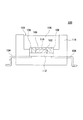
図4は、発光ダイオード素子102及び蛍光体層106の詳細な構成の一例を、基板112、キャビティ109、保持部118、及び封止部材108と共に示す。本例において、発光ダイオード素子102は、複数の電極412a、b、サファイア基板410、及び半導体層408を有し、サファイア基板410と基板112とが半導体層408を挟んで対向するように、基板112上に、フリップチップ実装される。電極412a、bは、例えば半田バンプであり、半導体層408と基板112とを、電気的に接続する。
FIG. 4 shows an example of detailed configurations of the light emitting
サファイア基板410は、1.8程度(例えば1.75〜1.85)の屈折率を有し、半導体層408が発生する光を、封止部材108に向かって透過する。そして、サファイア基板410は、透過した光を、封止部材108と対向する対向面110から、封止部材108へ出射する。これにより、発光ダイオード素子102は、対向面110を発光面116として、光を発生する。この場合、封止部材108は、サファイア基板410から入射する光を、対向面110と平行な出射面120(図3参照)から、LEDモジュール100(図3参照)の外部へ出射する。
The
また、本例において、サファイア基板410の対向面110には、拡大図154に示すような、サブ波長格子132(SWG:Subwavelength Grating)が形成されている。サブ波長格子132は、サファイア基板410が透過する光の波長よりも小さな格子周期で形成されることにより、対向面110における光の反射を低減させる。尚、拡大図154は、斜め上方から見た場合のサブ波長格子132を示す。
In this example, a sub-wavelength grating 132 (SWG: Subwavelength Grating) as shown in an
半導体層408は、例えば2.2〜2.5程度の屈折率を有し、サファイア基板410に向かって光を発生する。半導体層408は、例えば2〜4程度の屈折率を有してもよい。また、半導体層408は、サファイア基板410における、対向面110の裏面114上に結晶成長させることにより形成される。
The
本例において、半導体層408は、N型GaN層402、InGaN層404、及びP型GaN層406を有する。N型GaN層402、InGaN層404、及びP型GaN層406は、サファイア基板410の裏面114上に、順次積層して形成される。半導体層408は、これらの層の間に、更に別の層を有してもよい。
In this example, the
N型GaN層402は、サファイア基板410の裏面114上に積層して形成され、電極412bにより、基板112と接続される。N型GaN層402は、例えばAlxInyGa1−x−yN(0≦x≦1、0≦y≦1、x+y≦1)緩衝層を挟んで、サファイア基板410上に形成されてもよい。
The N-
InGaN層404は、発光層として機能する活性層であり、N型GaN層402上に積層して形成される。この場合、InGaN層404は、N型又はP型のドーパント、好ましくはSiがドープされることにより形成される。InGaN層404は、例えばN型AlGaN層を挟んで、N型GaN層402上に形成されてよい。
The
P型GaN層406は、InGaN層404上に積層して形成され、電極412aにより、基板112と接続される。P型GaN層406は、例えばP型AlGaN層を挟んで、InGaN層404上に形成されてよい。
The P-
これにより、半導体層408は、電極412a、b、及び基板112を介して受け取る電力に応じて、例えば波長が360〜380nm程度の紫外光を、サファイア基板410に向かって発生する。
Thereby, the
尚、半導体層408は、上記以外の周知の層構造を有してもよい。例えば、半導体層408は、上記以外のGaN系の半導体により形成されてよい。ここで、GaN系の半導体とは、例えば、AlxInyGa1−x−yN(0≦x≦1、0≦y≦1、x+y≦1)である。GaN系の半導体は、不純物をドープしない無添加層でN型層として用いられてもよく、アクセプター、ドナーの各ドーパントを添加することにより、各導電型のGaN系の半導体層として用いられてもよい。この場合、N型の不純物としては、Si、Ge、Sn等を、更に好ましくはSiを用いてよい。また、P型の不純物としては、特に限定されないが、Be、Zn、Mn、Cr、Mg、Ca等を、更に好ましくはMgが用いてよい。また、他の例において、半導体層408は、サファイア基板410に向かって、青色光を発生してもよい。
Note that the
蛍光体層106は、半導体層408が発生する紫外光に応じて蛍光することにより可視光を発生する。本例において、蛍光体層106は、蛍光体粒子602及びバインダ604を有する。本例において、蛍光体粒子602は、例えば2〜3程度の屈折率を有する。バインダ604は、例えば1.3〜1.6程度の屈折率を有する。
The
また、蛍光体粒子602は、紫外光に応じて可視光を発生する。バインダ604は、例えばシリコン樹脂又はフッ素系樹脂等により形成され、内部に蛍光体粒子602を収容することにより、蛍光体粒子602を、サファイア基板410の対向面110上に保持する。これにより、蛍光体層106は、サファイア基板410の対向面110上に設けられる。この場合、封止部材108は、蛍光体層106を挟んでサファイア基板410の対向面110と対向する。
The
そのため、蛍光体層106の屈折率は、サファイア基板410の屈折率より小さく、かつ封止部材108の屈折率より大きいのが好ましい。この場合、半導体層408が発生する紫外光を、高い効率で蛍光体層106に入射させ、かつ蛍光体層106が発生する光を、高い効率で、封止部材108に入射させることができる。尚、蛍光体層106の屈折率とは、例えば、蛍光体層106の界面における屈折率である。蛍光体層106の界面における屈折率は、内部の蛍光体粒子の屈折率の影響が小さいため、蛍光体層106におけるバインダの屈折率とほぼ同じであり、例えば1.3〜1.6程度である。
Therefore, the refractive index of the
また、本例において、蛍光体層106は、それぞれ異なる色の光を発生する複数種類の蛍光体粒子602を有する。それぞれの種類の蛍光体粒子602は、紫外光に応じて、赤色光、緑色光、及び青色光のそれぞれを発生する。これにより、蛍光体層106は、紫外光に応じて、白色光を発生する。また、この場合、蛍光体層106が3原色の光を発生するため、演色性の高い白色光を発生することができる。
In this example, the
ここで、半導体層408が、青色光を発生する場合、蛍光体層106は、半導体層408が発生する青色光に応じて蛍光することにより、黄色光を発生してよい。この場合も、発光ダイオード素子102及び蛍光体層106は、互いに補色関係にある青色光及び黄色光を発生することにより、白色光を発生する。また、この場合、サファイア基板410は、半導体層408が発生する青色光を透過して、対向面110から、封止部材108へ出射する。
Here, when the
以下、サブ波長格子132について更に詳しく説明する。本例において、サブ波長格子132は、対向面110と垂直な方向に突出する複数の凸部134を有する。この場合、回折波が発生しないことにより、サファイア基板410の内部から対向面110に入射する光に対して、サブ波長格子132は、サファイア基板410の内部と外部との中間の有効屈折率の媒体と等価となる。
Hereinafter, the
ここで、封止部材108から空気中へ、光を効率よく取り出すためには、封止部材108は、例えば1.4以下程度の、空気と近い屈折率を有するのが好ましい。しかし、この場合、対向面110において、サファイア基板410の内部と外部との屈折率の差が大きくなる場合がある。そのため、この場合に、例えばサブ波長格子132を用いずに、サファイア基板410の内部から光を出射させようとすれば、対向面110において、屈折率の不連続な変化が生じることとなる。この場合、対向面110における光の全反射により、サファイア基板410から光を効率よく取り出せない場合がある。
Here, in order to efficiently extract light from the sealing
しかし、本例において、サブ波長格子132は、サファイア基板410の内部と外部との中間の有効屈折率を有する。そのため、本例によれば、対向面110における、光の反射を低減させることができる。また、これにより、サファイア基板410から、光を効率よく取り出すことができる。そのため、本例によれば、光の取り出し効率が高いLEDモジュール100を提供することができる。
However, in this example, the
また、対向面110にサブ波長格子132を形成しないとすると、発光ダイオード素子102が発生する光を効率よく封止部材108に取り出すためには、封止部材108の屈折率を、発光ダイオード素子102と同程度に高くすることが必要となる場合がある。しかし、この場合、封止部材108から空気中へ適切に光を取り出すためには、出射面120(図3参照)を例えば球面状にする必要が生じる場合がある。また、封止部材108に適し、かつ発光ダイオード素子102と同程度に高い屈折率を有する樹脂においては、紫外線耐性が低い場合がある。
Further, if the
しかし、本例によれば、対向面110にサブ波長格子132を形成することにより、封止部材108を、例えば屈折率が1〜1.4程度の素材により形成することができる。この場合、封止部材108と空気との屈折率の差が小さいため、出射面120を平面状に形成することができる。そのため、本例によれば、出射面120を、低いコストで、高精度に形成することができる。また、本例によれば、封止部材108の屈折率を1〜1.4程度とできるため、封止部材108を、シリコン樹脂又はフッ素系樹脂等のような、紫外線耐性が高い素材により形成することができる。
However, according to this example, by forming the
尚、複数の凸部134は、サファイア基板410の対向面110に対するエッチングにより形成される。このエッチングにおいては、例えば、複数の凸部134に対応するレジストパターンが、エッチングマスクとして用いられる。また、このレジストパターンは、例えば電子ビームリソグラフィー法によるパターン描写により形成される。
The plurality of
ここで、他の例においては、サブ波長格子132を、例えば半導体層408の表面に形成することも考えられる。しかし、半導体層408の表面は、電極412等が形成されるため、サファイア基板410の対向面110と比べ、平坦性が低い場合がある。この場合、例えば電極412が形成されている部分の凹凸等に起因して、高い精度で均一なレジスト膜を形成するのが困難となる場合がある。また、この場合、例えば電子ビームリソグラフィー法を用いたとしても、レジストパターンを高精度に形成するのが困難となる場合がある。
Here, in another example, it is conceivable to form the
しかし、本例において、サブ波長格子132は、平坦性が高いサファイア基板410の対向面110上に形成される。そのため、本例によれば、高い精度で、サブ波長格子132を形成することができる。また、これにより、光の取り出し効率が高いLEDモジュール100を、適切に形成することができる。
However, in this example, the
図5は、サブ波長格子132の機能の一例を説明する図である。本例において、サファイア基板410の屈折率はn1である。また、蛍光体層106の屈折率はn2である。サブ波長格子132におけるそれぞれの凸部134は、四角錐状であり、対向面110と垂直な高さの方向(z軸)に対して、断面積が漸減する。
FIG. 5 is a diagram for explaining an example of the function of the
ここで、サブ波長格子132の有効屈折率は、サファイア基板410の媒質と、蛍光体層106との体積占有率に応じて変化する。そのため、本例において、サブ波長格子132の有効屈折率は、凸部134の底面からの距離zに応じて、サファイア基板410の屈折率n1から蛍光体層106の屈折率はn2へ、徐々に変化する。これにより、対向面110におけるサファイア基板410の内部と外部との屈折率差を滑らかに整合させることができる。そのため、本例によれば、対向面110における反射を低減することができる。
Here, the effective refractive index of the
ここで、複数の凸部134は、サファイア基板410が透過する光の半波長より小さな格子間隔Δx、Δyで配列されるのが好ましい。例えば、複数の凸部134の格子間隔は、サファイア基板410中における紫外光の半波長よりも小さくてよい。凸部134の高さhは、サファイア基板410が透過する光の半波長より大きいのが好ましい。この場合、凸部134の高さhは、蛍光体層106中における紫外光の半波長よりも大きくてよい。この場合、対向面110における反射を更に適切に低減することができる。
Here, it is preferable that the plurality of
ここで、発光ダイオード素子102が青色光を発生する場合、複数の凸部134の格子間隔Δx、Δyは、サファイア基板410中における青色光の半波長よりも小さくてよい。また、凸部134の高さhは、蛍光体層106中における青色光の半波長よりも大きくてよい。また、他の例において、凸部134は、例えば円錐状、又は他の多角錐状であってもよい。凸部134は、高さ方向に対して徐々に断面積が減少するテーパー状に形成されるのが好ましい。また、凸部134のアスペクト比は、1以上であるのが好ましい。
Here, when the light emitting
図6は、LEDモジュール100を製造する製造方法の一例を示すフローチャートである。本製造方法においては、最初に、サファイア基板410を準備する(S102)。そして、サファイア基板410の一方の面に、サブ波長格子132を形成する(S104)。本例において、サブ波長格子132は、サファイア基板410における、対向面110となるべき面に形成される。
FIG. 6 is a flowchart illustrating an example of a manufacturing method for manufacturing the
そして、サファイア基板410の裏面に対して、例えばエピタキシャル結晶成長法により、半導体層408を形成する(S106)。これにより、発光ダイオード素子102が形成される。尚、サファイア基板410の裏面とは、対向面110となるべき面の裏面である。
Then, a
次に、例えば保持部118に保持された基板112上に、発光ダイオード素子102を実装し(S108)、例えば蛍光体粒子602を含むバインダ604をキャビティ109中に充填することにより、蛍光体層106を形成する(S110)。
Next, for example, the light emitting
そして、次に、発光ダイオード素子102及び蛍光体層106を封止するように、封止部材108を形成して(S112)、本例の製造方法は、フローチャートを終了する。本例によれば、LEDモジュール100を適切に形成することができる。
Then, a sealing
ここで、S106において半導体層408を形成する工程は、エピタキシャル結晶成長法を用いるため、他の工程と比べ、多くの所要時間と高い精度を要する場合がある。そのため、サブ波長格子132の形成を、例えば半導体層408を形成した後に行うとすれば、例えばサブ波長格子132形成の歩留まりが低下した場合に、LEDモジュール100の製造コストが大きく上昇する場合がある。
Here, since the process of forming the
しかし、本例において、サブ波長格子132は、サファイア基板410に形成されるため、半導体層408よりも先に形成される。この場合、例えばサブ波長格子132の形成に失敗したとしても、例えばそのサファイア基板410を廃棄することにより、以降の工程を省略することができる。そのため、本例によれば、LEDモジュール100の生産コストを低減することができる。
However, in this example, since the
図7及び図8は、光源ユニット20の構成の一例を示す。図7は、光源ユニット20のAA垂直断面図である。図8は、光源ユニット20のBB垂直断面図である。光源ユニット20は、LEDモジュール100が発生する光を、車両の前方に照射する直射型の光源ユニットであり、LEDモジュール100、基板500、固定部材202、レンズ204、エクステンション208、及びハウジング206を有する。
7 and 8 show an example of the configuration of the
LEDモジュール100は、発光ダイオード素子102の発光面116における一辺とレンズ204の光軸とが直交するように、基板500上に固定される。また、発光ダイオード素子102は、ケーブル22及び基板500を介して光源ユニット20の外部から受け取る電力に基づき、発光面116から光を発生する。本例において、発光ダイオード素子102の発光面116は、サファイア基板410(図4参照)の対向面110である。
The
基板500は、例えば表面又は内部等に形成されたプリント配線により、LEDモジュール100と、ケーブル22とを電気的に接続する。本例において、基板500は、LEDモジュール100を裁置して固定する板状体であり、LEDモジュール100を、予め定められた基準位置に固定する。基板500の少なくとも一部は、例えば金属等の、空気よりも熱伝導率が高い素材により形成される。また、基板500の少なくとも一部は、固定部材202と接触する。これにより、基板500は、LEDモジュール100が発生する熱を、固定部材202に伝達する。
The
固定部材202は、例えば車両の前方を向く表面を有する板状体である。固定部材202は、レンズ204に対する相対位置が既知の位置に設けられる。また、固定部材202は、基板500を挟んでLEDモジュール100と対向するように、その表面上に、基板500を固定する。これにより、固定部材202は、LEDモジュール100を、車両の前方に向けて固定し、車両の前方に向けて発光させる。
The fixing
また、固定部材202は、例えば金属等の、空気よりも熱伝導率が高い素材により形成され、一端において、ハウジング206と接触する。これにより、固定部材202は、LEDモジュール100が発生する熱をハウジング206に伝達して、LEDモジュール100を放熱する。これにより、LEDモジュール100の発光量が熱により低下するのを防ぐことができる。
The fixing
エクステンション208は、例えば薄い金属板等により、LEDモジュール100の近傍から、レンズ204の縁部の近傍に渡って形成される。これにより、エクステンション208は、ハウジング206の内面と、LEDモジュール100との間の隙間を覆い隠し、車両用灯具10(図1参照)の見栄えを向上させる。エクステンション208は、LEDモジュール100が発生する光を反射してもよい。
The
ハウジング206は、LEDモジュール100、基板500、固定部材202、及びエクステンション208を収容する筐体である。また、ハウジング206は、前面に開口部を有し、この開口部においてレンズ204を保持する。ハウジング206は、基板500及び固定部材202を介してLEDモジュール100から受け取る熱を、放熱部材24(図1参照)及び/又はエクステンションリフレクタ28(図1参照)に更に伝達してよい。これにより、LEDモジュール100を、適切に放熱することができる。
The
レンズ204は、車両用灯具10に用いられる光学部材の一例であり、LEDモジュール100からの光を、車両用灯具10の外部に照射する。本例において、レンズ204は、発光ダイオード素子102の発光面116の形状を車両の前方に投影することにより、配光パターンの少なくとも一部を形成する。また、レンズ204は、発光面116の一辺の上に、光学的中心の一例である焦点Fを有する。この場合、レンズ204は、例えば、この直線状の境界の形状に基づき、配光パターンの明暗境界を規定するカットラインの少なくとも一部を形成する。本例によれば配光パターンを適切に形成することができる。
The
尚、本例のLEDモジュール100において、封止部材108の出射面120は、平面状に形成されている。しかし、他の例において、出射面120が例えば球面状だとすれば、レンズ204から見た発光面116は、レンズ状の封止部材108により拡大された像となる。この場合、高い精度で配光パターンを形成するためには、発光ダイオード素子102に対してレンズ204よりも近い位置にある封止部材108を、例えばレンズ204よりも高い精度で形成することが必要になる場合がある。また、これにより、LEDモジュール100のコストが上昇する場合がある。また、発光ダイオード素子102の拡大像の大きさを考慮してLEDモジュール100の位置あわせを行う必要が生じ、高い精度での位置合わせが困難になる場合がある。
In the
しかし、本例によれば、サファイア基板410(図4参照)の対向面110にサブ波長格子132を形成することにより、平面状の出射面120を有する封止部材108を用いることができる。そのため、本例によれば、高い精度で配光パターンを形成する車両用灯具10を、低いコストで提供することができる。また、拡大されていない実寸の発光ダイオード素子102を観察しながらLEDモジュール100の位置あわせを行うことにより、レンズ204に対するLEDモジュール100の位置を、簡易かつ高精度に合わせることができる。
However, according to this example, the sealing
図9は、車両用灯具10(図1参照)により形成される配光パターン300の一例を示す概念図である。配光パターン300は、車両用灯具10の前方25mの位置に配置された仮想鉛直スクリーン上に形成されるロービーム配光パターンである。本例において、車両用灯具10は、略水平方向の明暗境界を定める水平カットライン302、及び水平方向に対して15°程度の角度をなす所定の斜め方向の明暗境界を定める斜めカットライン304を有する配光パターン300を形成する。
FIG. 9 is a conceptual diagram showing an example of a
本例において、車両用灯具10は、それぞれ異なる配光特性を有する複数の光源ユニット20備え、それぞれの光源ユニット20が発生する光に基づき、配光パターン300を形成する。この場合、それぞれの光源ユニット20は、配光パターン300における一部の領域を形成する。例えば、図7及び図8を用いて説明した光源ユニット20は、配光パターン300の一部の領域306を形成する。
In this example, the
以下、図7及び図8を用いて説明した光源ユニット20の配光特性について、更に詳しく説明する。本例において、この光源ユニット20におけるレンズ204は、発光ダイオード素子102が発生する光を前方に照射することにより、発光ダイオード素子102の発光面116の形状を車両の前方に投影し、領域306を形成する。レンズ204は、この発光面116の形状を、水平方向に拡大して、投影してよい。
Hereinafter, the light distribution characteristics of the
ここで、本例において、レンズ204は、発光面116の一辺310の上に焦点Fを有している。辺310は、発光面116における、水平方向に延伸する下辺である。また、レンズ204は、発光ダイオード素子102が発生する光を、光源ユニット20の光軸を交差させて照射する。そのため、レンズ204は、発光面116の辺310の形状を、領域306の上辺の位置に投影する。
Here, in this example, the
また、レンズ204は、領域306の上辺の少なくとも一部を、水平カットライン302の少なくとも一部を形成すべき位置に形成する。これにより、光源ユニット20は、領域306により形成される明暗境界に基づき、水平カットライン302の少なくとも一部を形成する。本例によれば、配光パターンを適切に形成することができる。
The
図10は、LEDモジュール100の構成の更なる他の例を示す。尚、以下に説明する点を除き、図10において、図3と同一の符号を付した構成は、図3における構成と同一又は同様の機能を有するため、説明を省略する。本例において、LEDモジュール100は、複数の発光ダイオード素子102を有する。蛍光体層106は、複数の発光ダイオード素子102を覆うように設けられる。封止部材108は、複数の発光ダイオード素子102、及び蛍光体層106を封止する。
FIG. 10 shows still another example of the configuration of the
また、それぞれの発光ダイオード素子102におけるサファイア基板410の対向面110(図4参照)には、サブ波長格子132(図4参照)が形成されている。そのため、本例においても、発光ダイオード素子102は、蛍光体層106及び封止部材108へ、効率よく光を発生することができる。
A sub-wavelength grating 132 (see FIG. 4) is formed on the opposing surface 110 (see FIG. 4) of the
以上、本発明を実施の形態を用いて説明したが、本発明の技術的範囲は上記実施の形態に記載の範囲には限定されない。上記実施の形態に、多様な変更または改良を加えることが可能であることが当業者に明らかである。その様な変更または改良を加えた形態も本発明の技術的範囲に含まれ得ることが、特許請求の範囲の記載から明らかである。 As mentioned above, although this invention was demonstrated using embodiment, the technical scope of this invention is not limited to the range as described in the said embodiment. It will be apparent to those skilled in the art that various modifications or improvements can be added to the above-described embodiment. It is apparent from the scope of the claims that the embodiments added with such changes or improvements can be included in the technical scope of the present invention.
10・・・車両用灯具、12・・・カバー、14・・・ランプボディ、16・・・回路ユニット、20・・・光源ユニット、22・・・ケーブル、24・・・放熱部材、26・・・ケーブル、28・・・エクステンションリフレクタ、100・・・LEDモジュール、102・・・発光ダイオード素子、104・・・電極、106・・・蛍光体層、108・・・封止部材、109・・・キャビティ、110・・・対向面、112・・・基板、114・・・裏面、116・・・発光面、118・・・保持部、120・・・出射面、132・・・サブ波長格子、134・・・凸部、154・・・拡大図、202・・・固定部材、204・・・レンズ、206・・・ハウジング、208・・・エクステンション、300・・・配光パターン、302・・・水平カットライン、304・・・斜めカットライン、306・・・領域、310・・・辺、402・・・N型GaN層、404・・・InGaN層、406・・・P型GaN層、408・・・半導体層、410・・・サファイア基板、412・・・電極、500・・・基板、602・・・蛍光体粒子、604・・・バインダ
DESCRIPTION OF
Claims (8)
光を発生する半導体発光素子と、
前記発光モジュールが発生する光を透過する素材で、前記半導体発光素子を封止する封止部材と
を備え、
前記半導体発光素子は、
前記封止部材に向かって光を透過して、透過した光を、前記封止部材と対向する対向面から出射するサファイア基板であって、前記対向面に、前記サファイア基板が透過する光の波長よりも小さな格子周期で形成されることにより、光の反射を低減させるサブ波長格子が形成されているサファイア基板と、
前記サファイア基板における、前記対向面の裏面上に結晶成長させることにより形成されており、前記サファイア基板に向かって光を発生する半導体層と
を有する発光モジュール。 A light emitting module for generating light,
A semiconductor light emitting device for generating light;
A material that transmits light generated by the light emitting module, and a sealing member that seals the semiconductor light emitting element,
The semiconductor light emitting element is
A sapphire substrate that transmits light toward the sealing member and emits the transmitted light from a facing surface facing the sealing member, the wavelength of light transmitted by the sapphire substrate on the facing surface A sapphire substrate on which a sub-wavelength grating that reduces reflection of light is formed by a smaller grating period,
A light emitting module, comprising: a semiconductor layer that is formed by crystal growth on the back surface of the facing surface of the sapphire substrate and generates light toward the sapphire substrate.
前記複数の凸部は、前記サファイア基板が透過する光の半波長より小さな格子間隔で配列され、
前記凸部の高さは、前記サファイア基板が透過する光の半波長より大きい請求項1に記載の発光モジュール。 The sub-wavelength grating has a plurality of protrusions protruding in a direction perpendicular to the facing surface,
The plurality of convex portions are arranged at a lattice interval smaller than a half wavelength of light transmitted through the sapphire substrate,
The height of the said convex part is a light emitting module of Claim 1 larger than the half wavelength of the light which the said sapphire substrate permeate | transmits.
前記サファイア基板は、前記半導体層が発生する紫外光を透過して、前記対向面から、前記封止部材へ出射し、
前記発光モジュールは、前記半導体層が発生する紫外光に応じて蛍光することにより可視光を発生する、前記サファイア基板の前記対向面上に設けられた蛍光体層を更に備え、
前記封止部材は、前記蛍光体層を挟んで前記サファイア基板の前記対向面と対向し、
前記蛍光体層は、前記サファイア基板よりも小さな屈折率を有し、
前記複数の凸部の前記格子間隔は、前記サファイア基板中における前記紫外光の半波長よりも小さく、
前記凸部の高さは、前記蛍光体層中における前記紫外光の半波長よりも大きい請求項2に記載の発光モジュール。 The semiconductor layer generates ultraviolet light toward the sapphire substrate,
The sapphire substrate transmits ultraviolet light generated by the semiconductor layer, and is emitted from the facing surface to the sealing member.
The light emitting module further includes a phosphor layer provided on the facing surface of the sapphire substrate, which generates visible light by fluorescing according to ultraviolet light generated by the semiconductor layer,
The sealing member is opposed to the facing surface of the sapphire substrate with the phosphor layer interposed therebetween,
The phosphor layer has a smaller refractive index than the sapphire substrate,
The lattice spacing of the plurality of convex portions is smaller than the half wavelength of the ultraviolet light in the sapphire substrate,
The light emitting module according to claim 2, wherein a height of the convex portion is larger than a half wavelength of the ultraviolet light in the phosphor layer.
前記サファイア基板は、前記半導体層が発生する青色光を透過して、前記対向面から、前記封止部材へ出射し、
前記発光モジュールは、前記半導体層が発生する青色光に応じて蛍光することにより黄色光を発生する、前記サファイア基板の前記対向面上に設けられた蛍光体層を更に備え、
前記封止部材は、前記蛍光体層を挟んで前記サファイア基板の前記対向面と対向し、
前記蛍光体層は、前記サファイア基板よりも小さな屈折率を有し、
前記複数の凸部の前記格子間隔は、前記サファイア基板中における前記青色光の半波長よりも小さく、
前記凸部の高さは、前記蛍光体層中における前記青色光の半波長よりも大きい請求項2に記載の発光モジュール。 The semiconductor layer generates blue light toward the sapphire substrate,
The sapphire substrate transmits blue light generated by the semiconductor layer, and is emitted from the facing surface to the sealing member.
The light emitting module further includes a phosphor layer provided on the facing surface of the sapphire substrate, which generates yellow light by fluorescing according to blue light generated by the semiconductor layer,
The sealing member is opposed to the facing surface of the sapphire substrate with the phosphor layer interposed therebetween,
The phosphor layer has a smaller refractive index than the sapphire substrate,
The lattice spacing of the plurality of convex portions is smaller than the half wavelength of the blue light in the sapphire substrate,
The light emitting module according to claim 2, wherein a height of the convex portion is larger than a half wavelength of the blue light in the phosphor layer.
前記封止部材は、前記サファイア基板の前記対向面と平行な出射面を有し、前記サファイア基板から入射する光を、前記発光モジュールの外部へ、前記出射面から出射する請求項1に記載の発光モジュール。 The refractive index of the sealing member is larger than the refractive index of air and 1.4 or less,
The said sealing member has an output surface parallel to the said opposing surface of the said sapphire substrate, and outputs the light which injects from the said sapphire substrate from the said output surface to the exterior of the said light emitting module. Light emitting module.
前記サファイア基板は、前記半導体層が発生する紫外光を透過して、前記対向面から、前記封止部材へ出射し、
前記発光モジュールは、前記半導体層が発生する紫外光に応じて蛍光することにより可視光を発生する、前記サファイア基板の前記対向面上に設けられた蛍光体層を更に備え、
前記蛍光体層の屈折率は、前記サファイア基板の屈折率より小さく、かつ前記封止部材の屈折率より大きく、
前記封止部材は、シリコン樹脂又はフッ素系樹脂により形成された請求項1に記載の発光モジュール。 The semiconductor layer generates ultraviolet light toward the sapphire substrate,
The sapphire substrate transmits ultraviolet light generated by the semiconductor layer, and is emitted from the facing surface to the sealing member.
The light emitting module further includes a phosphor layer provided on the facing surface of the sapphire substrate, which generates visible light by fluorescing according to ultraviolet light generated by the semiconductor layer,
The refractive index of the phosphor layer is smaller than the refractive index of the sapphire substrate and larger than the refractive index of the sealing member,
The light emitting module according to claim 1, wherein the sealing member is formed of a silicon resin or a fluorine resin.
光を発生する発光モジュールと、
前記発光モジュールからの光を前記灯具の外部へ照射する光学部材と
を備え、
前記発光モジュールは、
光を発生する半導体発光素子と、
前記発光モジュールが発生する光を透過する素材で、前記半導体発光素子を封止する封止部材と
を有し、
前記半導体発光素子は、
前記封止部材に向かって光を透過して、透過した光を、前記封止部材と対向する対向面から出射するサファイア基板であって、前記対向面に、前記サファイア基板が透過する光の波長よりも小さな格子周期で形成されることにより、光の反射を低減させるサブ波長格子が形成されているサファイア基板と、
前記サファイア基板における、前記対向面の裏面上に結晶成長させることにより形成されており、前記サファイア基板に向かって光を発生する半導体層と
を含む灯具。 A lamp that generates light,
A light emitting module that generates light;
An optical member for irradiating the light from the light emitting module to the outside of the lamp,
The light emitting module
A semiconductor light emitting device for generating light;
A material that transmits light generated by the light emitting module, and a sealing member that seals the semiconductor light emitting element,
The semiconductor light emitting element is
A sapphire substrate that transmits light toward the sealing member and emits the transmitted light from a facing surface facing the sealing member, the wavelength of light transmitted by the sapphire substrate on the facing surface A sapphire substrate on which a sub-wavelength grating that reduces reflection of light is formed by a smaller grating period,
A lamp including a semiconductor layer that is formed by crystal growth on the back surface of the facing surface of the sapphire substrate and generates light toward the sapphire substrate.
前記封止部材の屈折率は、空気の屈折率よりも大きく、かつ1.4以下であり、
前記封止部材は、前記サファイア基板の前記対向面と平行な出射面を有し、前記サファイア基板から入射する光を、前記発光モジュールの外部へ、前記出射面から出射し、
前記光学部材は、前記サファイア基板の前記対向面の形状を投影することにより、前記前照灯の配光パターンの明暗境界を定めるカットラインの少なくとも一部を形成する請求項7に記載の灯具。 The lamp is a lamp used for a headlamp of a vehicle,
The refractive index of the sealing member is larger than the refractive index of air and 1.4 or less,
The sealing member has an emission surface parallel to the facing surface of the sapphire substrate, and emits light incident from the sapphire substrate to the outside of the light emitting module from the emission surface,
The said optical member is a lamp of Claim 7 which forms at least one part of the cut line which defines the light-dark boundary of the light distribution pattern of the said headlamp by projecting the shape of the said opposing surface of the said sapphire board | substrate.
Priority Applications (2)
| Application Number | Priority Date | Filing Date | Title |
|---|---|---|---|
| JP2004013123A JP2005209794A (en) | 2004-01-21 | 2004-01-21 | Light emitting module and lamp |
| US11/033,872 US7282747B2 (en) | 2004-01-21 | 2005-01-13 | Light emitting module and lamp |
Applications Claiming Priority (1)
| Application Number | Priority Date | Filing Date | Title |
|---|---|---|---|
| JP2004013123A JP2005209794A (en) | 2004-01-21 | 2004-01-21 | Light emitting module and lamp |
Publications (1)
| Publication Number | Publication Date |
|---|---|
| JP2005209794A true JP2005209794A (en) | 2005-08-04 |
Family
ID=34747351
Family Applications (1)
| Application Number | Title | Priority Date | Filing Date |
|---|---|---|---|
| JP2004013123A Pending JP2005209794A (en) | 2004-01-21 | 2004-01-21 | Light emitting module and lamp |
Country Status (2)
| Country | Link |
|---|---|
| US (1) | US7282747B2 (en) |
| JP (1) | JP2005209794A (en) |
Cited By (4)
| Publication number | Priority date | Publication date | Assignee | Title |
|---|---|---|---|---|
| JP2007294771A (en) * | 2006-04-26 | 2007-11-08 | Koito Mfg Co Ltd | Vehicle lamp unit |
| JP2011091257A (en) * | 2009-10-23 | 2011-05-06 | Stanley Electric Co Ltd | Method of manufacturing led light source device |
| JP2014068010A (en) * | 2012-09-24 | 2014-04-17 | Lg Innotek Co Ltd | Ultraviolet light emitting device |
| WO2017123040A1 (en) * | 2016-01-14 | 2017-07-20 | 피에스아이 주식회사 | Ultra-small led electrode assembly and method for preparing same |
Families Citing this family (18)
| Publication number | Priority date | Publication date | Assignee | Title |
|---|---|---|---|---|
| CN100379041C (en) * | 2003-08-07 | 2008-04-02 | 松下电器产业株式会社 | LED illumination light source and manufacturing method thereof |
| US8044412B2 (en) | 2006-01-20 | 2011-10-25 | Taiwan Semiconductor Manufacturing Company, Ltd | Package for a light emitting element |
| US20080055065A1 (en) * | 2006-08-30 | 2008-03-06 | David Charles Feldmeier | Systems, devices, components and methods for controllably configuring the brightness of light emitted by an automotive LED illumination system |
| US20080055896A1 (en) * | 2006-08-30 | 2008-03-06 | David Charles Feldmeier | Systems, devices, components and methods for controllably configuring the color of light emitted by an automotive LED illumination system |
| DE102007046339A1 (en) | 2007-09-27 | 2009-04-02 | Osram Opto Semiconductors Gmbh | Light source with variable emission characteristics |
| JP5336564B2 (en) | 2010-10-29 | 2013-11-06 | シャープ株式会社 | Light emitting device, lighting device, vehicle headlamp, and vehicle |
| JP5259791B2 (en) | 2010-10-29 | 2013-08-07 | シャープ株式会社 | Light emitting device, vehicle headlamp, lighting device, and vehicle |
| JP5487077B2 (en) * | 2010-10-29 | 2014-05-07 | シャープ株式会社 | Light emitting device, vehicle headlamp and lighting device |
| JP2012119193A (en) | 2010-12-01 | 2012-06-21 | Sharp Corp | Light-emitting device, vehicular headlamp, lighting device, and vehicle |
| US20120138981A1 (en) * | 2010-12-02 | 2012-06-07 | Chung-Shan Institute of Science and Technology, Armaments, Bureau, Ministry of National Defense | Light-Emitting Diode Apparatus and Method for Making the Same |
| JP5788194B2 (en) | 2011-03-03 | 2015-09-30 | シャープ株式会社 | Light emitting device, lighting device, and vehicle headlamp |
| CN102829416B (en) * | 2011-06-14 | 2015-07-22 | 财团法人工业技术研究院 | Luminaire light source with light-emitting diodes with multiple light-shape outputs |
| CN102853378B (en) | 2011-06-29 | 2015-09-02 | 夏普株式会社 | Projection device, and vehicle headlamp equipped with the projection device |
| AU2011101305B4 (en) * | 2011-10-11 | 2012-06-07 | Weidmuller Pty Ltd | Headlight assembly |
| AU2011101306B4 (en) * | 2011-10-11 | 2012-06-07 | Weidmuller Pty Ltd | Lighting assembly |
| JP2013172028A (en) * | 2012-02-21 | 2013-09-02 | Stanley Electric Co Ltd | Semiconductor light-emitting element and vehicle lamp fitting |
| DE202016105054U1 (en) * | 2016-09-12 | 2016-10-03 | Ridi Leuchten Gmbh | Lighting device for bulbs |
| TWI882886B (en) * | 2024-08-16 | 2025-05-01 | 巨鎧精密工業股份有限公司 | Headlights |
Family Cites Families (6)
| Publication number | Priority date | Publication date | Assignee | Title |
|---|---|---|---|---|
| TW383508B (en) | 1996-07-29 | 2000-03-01 | Nichia Kagaku Kogyo Kk | Light emitting device and display |
| US6367949B1 (en) * | 1999-08-04 | 2002-04-09 | 911 Emergency Products, Inc. | Par 36 LED utility lamp |
| TW465123B (en) * | 2000-02-02 | 2001-11-21 | Ind Tech Res Inst | High power white light LED |
| JP2002261333A (en) * | 2001-03-05 | 2002-09-13 | Toyoda Gosei Co Ltd | Light emitting device |
| US6813077B2 (en) * | 2001-06-19 | 2004-11-02 | Corning Incorporated | Method for fabricating an integrated optical isolator and a novel wire grid structure |
| DE10259945A1 (en) * | 2002-12-20 | 2004-07-01 | Tews, Walter, Dipl.-Chem. Dr.rer.nat.habil. | Phosphors with an extended fluorescence lifetime |
-
2004
- 2004-01-21 JP JP2004013123A patent/JP2005209794A/en active Pending
-
2005
- 2005-01-13 US US11/033,872 patent/US7282747B2/en not_active Expired - Fee Related
Cited By (6)
| Publication number | Priority date | Publication date | Assignee | Title |
|---|---|---|---|---|
| JP2007294771A (en) * | 2006-04-26 | 2007-11-08 | Koito Mfg Co Ltd | Vehicle lamp unit |
| JP2011091257A (en) * | 2009-10-23 | 2011-05-06 | Stanley Electric Co Ltd | Method of manufacturing led light source device |
| JP2014068010A (en) * | 2012-09-24 | 2014-04-17 | Lg Innotek Co Ltd | Ultraviolet light emitting device |
| WO2017123040A1 (en) * | 2016-01-14 | 2017-07-20 | 피에스아이 주식회사 | Ultra-small led electrode assembly and method for preparing same |
| US10784246B2 (en) | 2016-01-14 | 2020-09-22 | Samsung Display Co., Ltd. | Ultra-small LED electrode assembly and method for preparing same |
| US11380670B2 (en) | 2016-01-14 | 2022-07-05 | Samsung Display Co., Ltd. | Ultra-small LED electrode assembly and method for preparing same |
Also Published As
| Publication number | Publication date |
|---|---|
| US7282747B2 (en) | 2007-10-16 |
| US20050157508A1 (en) | 2005-07-21 |
Similar Documents
| Publication | Publication Date | Title |
|---|---|---|
| JP2005209794A (en) | Light emitting module and lamp | |
| US7385349B2 (en) | Light emitting module and lighting unit for vehicle | |
| JP4806025B2 (en) | Multifunctional automotive floodlight module, especially for the automotive front area | |
| US6855958B2 (en) | Wavelength conversion element for car use | |
| US8304800B2 (en) | Light emitting device, light emitting device package, and lighting device system | |
| US8253143B2 (en) | Light emitting module and method of manufacturing the same | |
| US8994051B2 (en) | Light emission module, light emission module manufacturing method, and lamp unit | |
| US8669575B2 (en) | Light emitting module, method of manufacturing the light emitting module, and lamp unit | |
| US7282748B2 (en) | Light emitting module and lamp | |
| TWI594464B (en) | Light-emitting component package | |
| US20100149816A1 (en) | Light emitting module, fabrication method therefor, and lamp unit | |
| CN102341740A (en) | Light emitting unit array, method of manufacturing the same, and projection apparatus | |
| JP2010287777A (en) | Light emitting module and vehicle headlamp | |
| CN101128942B (en) | LED array | |
| US8568007B2 (en) | Vehicle headlight | |
| TWI775911B (en) | Light emitting device package | |
| US20200287107A1 (en) | Light-emitting device package | |
| US20070253212A1 (en) | Vehicular lamp unit | |
| JP2009021418A (en) | Light emitting device | |
| US20100177527A1 (en) | Light emitting module, fabrication method therefor, and lamp unit | |
| JP7082666B2 (en) | Luminescent semiconductor device | |
| KR102432220B1 (en) | Semiconductor device and semiconductor module | |
| TWI894785B (en) | Light-emitting diode package | |
| CN101120203A (en) | lighting device | |
| JPWO2011078008A1 (en) | Vehicle headlamp |
Legal Events
| Date | Code | Title | Description |
|---|---|---|---|
| A621 | Written request for application examination |
Free format text: JAPANESE INTERMEDIATE CODE: A621 Effective date: 20050929 |
|
| A977 | Report on retrieval |
Free format text: JAPANESE INTERMEDIATE CODE: A971007 Effective date: 20080714 |
|
| A131 | Notification of reasons for refusal |
Free format text: JAPANESE INTERMEDIATE CODE: A131 Effective date: 20080722 |
|
| A521 | Request for written amendment filed |
Free format text: JAPANESE INTERMEDIATE CODE: A523 Effective date: 20080910 |
|
| A131 | Notification of reasons for refusal |
Free format text: JAPANESE INTERMEDIATE CODE: A131 Effective date: 20081202 |
|
| A521 | Request for written amendment filed |
Free format text: JAPANESE INTERMEDIATE CODE: A523 Effective date: 20090126 |
|
| A02 | Decision of refusal |
Free format text: JAPANESE INTERMEDIATE CODE: A02 Effective date: 20090414 |