JP2005136258A - Semiconductor device and manufacturing method thereof - Google Patents
Semiconductor device and manufacturing method thereof Download PDFInfo
- Publication number
- JP2005136258A JP2005136258A JP2003371729A JP2003371729A JP2005136258A JP 2005136258 A JP2005136258 A JP 2005136258A JP 2003371729 A JP2003371729 A JP 2003371729A JP 2003371729 A JP2003371729 A JP 2003371729A JP 2005136258 A JP2005136258 A JP 2005136258A
- Authority
- JP
- Japan
- Prior art keywords
- region
- drain
- source
- impurity layer
- gate electrode
- Prior art date
- Legal status (The legal status is an assumption and is not a legal conclusion. Google has not performed a legal analysis and makes no representation as to the accuracy of the status listed.)
- Pending
Links
Images


Classifications
-
- H10P30/204—
-
- H—ELECTRICITY
- H10—SEMICONDUCTOR DEVICES; ELECTRIC SOLID-STATE DEVICES NOT OTHERWISE PROVIDED FOR
- H10D—INORGANIC ELECTRIC SEMICONDUCTOR DEVICES
- H10D30/00—Field-effect transistors [FET]
- H10D30/01—Manufacture or treatment
- H10D30/021—Manufacture or treatment of FETs having insulated gates [IGFET]
- H10D30/0223—Manufacture or treatment of FETs having insulated gates [IGFET] having source and drain regions or source and drain extensions self-aligned to sides of the gate
- H10D30/0227—Manufacture or treatment of FETs having insulated gates [IGFET] having source and drain regions or source and drain extensions self-aligned to sides of the gate having both lightly-doped source and drain extensions and source and drain regions self-aligned to the sides of the gate, e.g. lightly-doped drain [LDD] MOSFET or double-diffused drain [DDD] MOSFET
-
- H—ELECTRICITY
- H10—SEMICONDUCTOR DEVICES; ELECTRIC SOLID-STATE DEVICES NOT OTHERWISE PROVIDED FOR
- H10D—INORGANIC ELECTRIC SEMICONDUCTOR DEVICES
- H10D62/00—Semiconductor bodies, or regions thereof, of devices having potential barriers
- H10D62/10—Shapes, relative sizes or dispositions of the regions of the semiconductor bodies; Shapes of the semiconductor bodies
- H10D62/17—Semiconductor regions connected to electrodes not carrying current to be rectified, amplified or switched, e.g. channel regions
- H10D62/351—Substrate regions of field-effect devices
- H10D62/357—Substrate regions of field-effect devices of FETs
- H10D62/364—Substrate regions of field-effect devices of FETs of IGFETs
- H10D62/371—Inactive supplementary semiconductor regions, e.g. for preventing punch-through, improving capacity effect or leakage current
-
- H10P30/212—
-
- H10P30/22—
-
- H10P30/225—
-
- H—ELECTRICITY
- H10—SEMICONDUCTOR DEVICES; ELECTRIC SOLID-STATE DEVICES NOT OTHERWISE PROVIDED FOR
- H10D—INORGANIC ELECTRIC SEMICONDUCTOR DEVICES
- H10D64/00—Electrodes of devices having potential barriers
- H10D64/01—Manufacture or treatment
- H10D64/015—Manufacture or treatment removing at least parts of gate spacers, e.g. disposable spacers
Landscapes
- Insulated Gate Type Field-Effect Transistor (AREA)
Abstract
【課題】電界効果トランジスタの短チャネル効果が十分に小さく、且つ、接合容量および接合リーク電流も十分に小さい半導体装置を提供する。
【解決手段】電界効果トランジスタ100は、シリコン基板110内に形成されたチャネル領域130と、チャネル領域130上にゲート絶縁膜140を介して形成されたゲート電極150と、高濃度不純物領域170と、ポケット領域180とを備える。ポケット領域180は、高濃度不純物領域170内からチャネル領域130内にわたって形成される。高濃度不純物領域170内のポケット領域181がこの高濃度不純物領域170の下端面173よりも浅い領域に位置しているので、接合容量および接合リーク電流が減少する。チャネル領域130内のポケット領域182がポケット領域181よりも深い領域に形成されるので、短チャネル効果が減少する。
【選択図】図1
Provided is a semiconductor device in which a short channel effect of a field effect transistor is sufficiently small, and a junction capacitance and a junction leakage current are also sufficiently small.
A field effect transistor includes a channel region formed in a silicon substrate, a gate electrode formed on the channel region via a gate insulating film, a high-concentration impurity region, Pocket area 180. The pocket region 180 is formed from the high concentration impurity region 170 to the channel region 130. Since the pocket region 181 in the high concentration impurity region 170 is located in a region shallower than the lower end surface 173 of the high concentration impurity region 170, the junction capacitance and the junction leakage current are reduced. Since the pocket region 182 in the channel region 130 is formed in a region deeper than the pocket region 181, the short channel effect is reduced.
[Selection] Figure 1
Description
本発明は、ポケット領域が設けられた電界効果トランジスタを有する半導体装置およびその製造方法に関する。 The present invention relates to a semiconductor device having a field effect transistor provided with a pocket region and a method for manufacturing the same.
従来、半導体装置に形成される電界効果トランジスタとして、サイドウォールの下にポケット領域を設けた電界効果トランジスタが知られている。ポケット領域は、ソース・ドレイン領域とは逆の導電型に形成される。ポケット領域を設けることにより、電界効果トランジスタの短チャネル効果を抑制することができる。ポケット領域を設けた電界効果トランジスタに関する文献としては、例えば、下記特許文献1〜3が知られている。 Conventionally, a field effect transistor in which a pocket region is provided under a sidewall is known as a field effect transistor formed in a semiconductor device. The pocket region is formed to have a conductivity type opposite to that of the source / drain region. By providing the pocket region, the short channel effect of the field effect transistor can be suppressed. For example, the following Patent Documents 1 to 3 are known as documents relating to a field effect transistor provided with a pocket region.
このような電界効果トランジスタにおいて、短チャネル効果を抑制するためには、ポケットの不純物濃度は大きいほど良く、また、ポケット領域の形成位置は深いほど良い。さらには、短チャネル効果を十分に抑制するためには、ポケット領域がゲート電極の直下にまで伸びて形成されていることが望ましい。 In such a field effect transistor, in order to suppress the short channel effect, the larger the impurity concentration in the pocket, the better the deeper the position where the pocket region is formed. Furthermore, in order to sufficiently suppress the short channel effect, it is desirable that the pocket region is formed so as to extend directly below the gate electrode.
ポケット領域の不純物濃度を大きくするためには、このポケット領域を形成する際のドーズ量を大きくすればよい。しかしながら、このドーズ量を大きくすると、ソース・ドレイン領域と基板との間の接合容量および接合リーク電流が増大してしまうという欠点が生じる。ポケット領域形成時のドーズ量を増大させることにより、ソース・ドレイン領域の下端面近傍において、基板の不純物濃度が増大してしまうからである。 In order to increase the impurity concentration of the pocket region, the dose amount in forming the pocket region may be increased. However, when this dose is increased, there is a disadvantage that the junction capacitance between the source / drain region and the substrate and the junction leakage current increase. This is because the impurity concentration of the substrate increases in the vicinity of the lower end surface of the source / drain region by increasing the dose amount when forming the pocket region.
基板の不純物濃度上昇を防止するためには、ポケット領域を、ソース・ドレイン領域の下端面よりも浅い位置に形成すればよい。しかしながら、上述のように、ポケット領域を浅い位置に形成すると、短チャネル効果の抑制効果が減少する。 In order to prevent an increase in the impurity concentration of the substrate, the pocket region may be formed at a position shallower than the lower end surface of the source / drain region. However, as described above, when the pocket region is formed at a shallow position, the effect of suppressing the short channel effect is reduced.
また、ゲート電極の直下にまで伸びるようにポケット領域を形成するために、従来は、斜めイオン注入法が利用されていた。しかしながら、ポケット領域形成時の斜めイオン注入を利用する場合、隣接する他のゲート電極が遮蔽して不純物が導入されない領域が発生してしまい、また、不純物が導入されない領域の面積がゲート電極の高さのばらつきに起因してばらついてしまうという問題が生じる。これらの問題が電界効果トランジスタの特性に影響を与えないようにするためには、イオン注入角度は30゜〜40゜程度以下に限定されてしまう。このため、斜めイオン注入法を用いてゲート電極直下にまで伸びるポケット領域を形成する方法では、短チャネル効果を十分に抑制することができなかった。
本発明の解決課題は、電界効果トランジスタの短チャネル効果が十分に小さく、且つ、接合容量および接合リーク電流も十分に小さい半導体装置およびその製造方法を提供することにある。 An object of the present invention is to provide a semiconductor device in which the short channel effect of a field effect transistor is sufficiently small, and a junction capacitance and a junction leakage current are sufficiently small, and a method for manufacturing the same.
本発明に係る半導体装置は、第1導電型の半導体基板と、半導体基板上にゲート絶縁膜を介して形成されたゲート電極と、半導体基板に形成されたソース及びドレインと、ソース内からゲート電極の直下にわたって形成された第1導電型のソース側不純物層及びドレイン内からゲート電極の直下にわたって形成された第1導電型のドレイン側不純物層とを有し、ソース側不純物層はソース内よりもゲート電極の直下において半導体基板の表面から深い位置に形成されており、ドレイン側不純物層はドレイン内よりもゲート電極の直下において半導体基板の表面から深い位置に形成されていることを特徴とする。 A semiconductor device according to the present invention includes a first conductivity type semiconductor substrate, a gate electrode formed on the semiconductor substrate via a gate insulating film, a source and a drain formed on the semiconductor substrate, and a gate electrode from within the source. A first-conductivity-type source-side impurity layer formed immediately below the drain electrode and a first-conductivity-type drain-side impurity layer formed directly from the inside of the drain to the gate electrode. The drain-side impurity layer is formed at a position deeper than the surface of the semiconductor substrate immediately below the gate electrode and directly below the gate electrode.
本発明に係る半導体装置の製造方法は、第1導電型の半導体基板にゲート絶縁膜及びゲート電極を形成する工程と、ゲート電極の側面にサイドウォールを形成する工程と、半導体基板の露出面に表面被覆膜を形成する工程と、半導体基板に不純物を導入することによってソース及びドレインを形成する工程と、サイドウォールを除去する工程と、サイドウォールが除去された面及び表面被覆膜を介して半導体基板に第1導電型の不純物を導入することによりソース側不純物層及びドレイン側不純物層を形成する工程とを有し、ソース側不純物層はソース内からゲート電極の直下にわたって延在し且つソース内よりもゲート電極の直下において半導体基板の表面から深い位置に形成し、ドレイン側不純物層はドレイン内からゲート電極の直下にわたって延在し、且つ、ドレイン内よりもゲート電極の直下において半導体基板の表面から深い位置に形成することを特徴とする。 A method of manufacturing a semiconductor device according to the present invention includes a step of forming a gate insulating film and a gate electrode on a first conductivity type semiconductor substrate, a step of forming a sidewall on a side surface of the gate electrode, and an exposed surface of the semiconductor substrate. A step of forming a surface coating film, a step of forming a source and a drain by introducing impurities into the semiconductor substrate, a step of removing the sidewall, and a surface and the surface coating film from which the sidewall has been removed. And forming a source-side impurity layer and a drain-side impurity layer by introducing a first conductivity type impurity into the semiconductor substrate, the source-side impurity layer extending from within the source to directly below the gate electrode, and It is formed deeper from the surface of the semiconductor substrate directly below the gate electrode than in the source, and the drain side impurity layer is directly under the gate electrode from within the drain. Tatte extend, and, and forming a deeper position from the surface of the semiconductor substrate immediately below the gate electrode than in the drain.
本発明に係る半導体装置では、ソース側不純物層及びドレイン側不純物層を、ソース・ドレイン内よりもゲート電極の直下において半導体基板の表面から深い位置になるように形成した。したがって、接合容量および接合リーク電流の増大を防止することができ且つ短チャネル効果を十分に抑制することができる。 In the semiconductor device according to the present invention, the source-side impurity layer and the drain-side impurity layer are formed so as to be deeper from the surface of the semiconductor substrate immediately below the gate electrode than in the source / drain. Therefore, increase in junction capacitance and junction leakage current can be prevented and the short channel effect can be sufficiently suppressed.
本発明に係る半導体装置の製造方法では、サイドウォールが除去された面および表面被覆膜を介して半導体基板内に不純物を導入することによってソース側不純物層及びドレイン側不純物層を形成することとしたので、これらソース側不純物層及びドレイン側不純物層を、ソース・ドレイン内よりもゲート電極の直下において半導体基板の表面から深い位置になるように形成することができる。本発明に係る半導体装置の製造方法によれば、本発明の半導体装置を、簡単な工程で安価に製造することができる。 In the method of manufacturing a semiconductor device according to the present invention, the source-side impurity layer and the drain-side impurity layer are formed by introducing impurities into the semiconductor substrate through the surface from which the sidewall has been removed and the surface coating film. Therefore, the source-side impurity layer and the drain-side impurity layer can be formed deeper from the surface of the semiconductor substrate immediately below the gate electrode than in the source / drain. According to the method for manufacturing a semiconductor device of the present invention, the semiconductor device of the present invention can be manufactured at a low cost by a simple process.
以下、この発明の実施の形態について、図面を用いて説明する。なお、図中、各構成成分の大きさ、形状および配置関係は、この発明が理解できる程度に概略的に示してあるにすぎず、また、以下に説明する数値的条件は単なる例示にすぎない。 Embodiments of the present invention will be described below with reference to the drawings. In the drawings, the size, shape, and arrangement relationship of each component are shown only schematically to the extent that the present invention can be understood, and the numerical conditions described below are merely examples. .
図1は、本実施形態の半導体装置に設けられるMOSFET(Metal-Oxide-Semiconductor Field Effect Transistor) 100の構造を概略的に示す断面図である。 FIG. 1 is a cross-sectional view schematically showing the structure of a MOSFET (Metal-Oxide-Semiconductor Field Effect Transistor) 100 provided in the semiconductor device of this embodiment.
図1に示したように、シリコン基板110には、フィールド酸化膜120、チャネル領域130、ゲート絶縁膜140、ゲート電極150、サイドウォール160、高濃度不純物領域(ソース・ドレイン領域)170、およびポケット領域180が形成される。
As shown in FIG. 1, the
フィールド酸化膜120は、素子分離膜すなわち素子形成領域と他の領域とを電気的に分離するため膜であり、素子形成領域の外周を覆うように形成される。
The
チャネル領域130は、半導体基板110の素子形成領域全域に、低濃度の不純物を導入することによって、形成される。例えば、n型MOSFETの場合にはボロンまたはBF2 が、p型MOSFETの場合にはヒ素またはリンが、チャネル領域130の不純物として使用される。
The
ゲート絶縁膜140は、チャネル領域130とゲート電極150との間を絶縁するための、薄い絶縁膜である。
The
ゲート電極150は、ゲート絶縁膜140上に、例えばポリシリコン等の導電性材料によって形成される。また、ゲート電極150をポリシリコンで形成する場合、n型MOSFETの場合にはリンまたはヒ素を、p型MOSFETの場合にはボロンまたはBF2 を、不純物として導入してもよい。このときの不純物濃度は、例えば、2×1015cm-3程度とすることができる。
The
サイドウォール160は、ゲート絶縁膜140およびゲート電極150の側面に形成される。
The
高濃度不純物領域170は、MOSFET100のソースおよびドレインをなす領域である。高濃度不純物領域170は、それぞれ、ゲート電極150を挟んで対向するように配置される。これらの高濃度不純物領域170は、それぞれ、チャネル領域130の深い位置まで形成された領域171と、サイドウォール160の直下に形成された浅いLDD(Lightly Doped Drain)領域172とを備える。周知のように、n型MOSFETの場合、高濃度不純物領域170は、ヒ素またはリンを不純物として用いて、p型に形成される。一方、p型MOSFETの場合、高濃度不純物領域170は、ボロンまたはBF2 を不純物として用いて、n型に形成される。
The high
ポケット領域180は、高濃度不純物領域170内からチャネル領域130内にわたって形成される。ポケット領域180は、チャネル領域130と同じ導電型、すなわち高濃度不純物領域170とは逆の導電型を備える。
The
ここで、高濃度不純物領域170内のポケット領域181は、高濃度不純物領域170の下端面173よりも浅い領域に位置するように形成される。これにより、ポケット領域180を形成する不純物が高濃度不純物領域170の下端面173に達することを防止し或いは減少させることができる。上述のように、チャネル領域130とポケット領域180とは同じ導電型である。したがって、高濃度不純物領域170の下端面173と重なるようにポケット領域180を形成すると、この下端面173との界面近傍における、チャネル領域130の不純物濃度が高くなる。そして、かかる部分の不純物濃度が高くなると、この部分で、高濃度不純物領域170とチャネル領域130との間の接合容量および接合リーク電流が増大してしまう。これに対して、本実施形態では、高濃度不純物領域170の下端面173よりも浅い領域に位置するようにポケット領域180を形成したので、この下端面173との界面近傍におけるチャネル領域130の不純物濃度を低く抑えることができる。一般に、高濃度不純物領域170の下端面173とチャネル領域130との界面の面積は、高濃度不純物領域170とチャネル領域130との界面の総面積の90%程度を占める。したがって、本実施形態によれば、接合容量および接合リーク電流を十分に低減させることができる。
Here, the
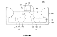
図2は、比較のためのMOSFET200の構造を概略的に示す断面図である。図2に示したMOSFET200は、高濃度不純物領域170の下端面173と重なるようにポケット領域180が形成されている点が、本実施形態のMOSFET100(図1参照)と異なっている。また、図3は、本実施形態のMOSFET100と比較用のMOSFET200との不純物濃度分布を比較するためのグラフである。図3において、縦軸は不純物濃度(この例ではヒ素)であり、横軸は深さである。図3から解るように、本実施形態のMOSFET100は、高濃度不純物領域170の下端面173と重ならないようにポケット領域180が形成されているので、下端面173におけるヒ素濃度(図3の符号A1参照)が、比較例のMOSFET200の下端面173におけるヒ素濃度(図3の符号B1参照)よりも、ΔDだけ小さくなる。
FIG. 2 is a cross-sectional view schematically showing the structure of a
また、チャネル領域130内のポケット領域182は、高濃度不純物領域170内に形成されたポケット領域181よりも深い領域に、形成される。上述のように、ポケット領域の形成位置は深いほど、短チャネル効果が小さくなる。したがって、本実施形態によれば、短チャネル効果を減らすことができる。チャネル領域130内に形成されたポケット領域182の下端面183は、高濃度不純物領域の下端面173と同じ深さまたは下端面183よりも深くなるように形成されることが望ましい。これにより、チャネル領域130内のポケット領域182が十分に深い位置に形成されることになるので、短チャネル効果を十分に小さく抑えることができる。
The
さらに、チャネル領域130内のポケット領域182は、ゲート電極150の直下領域内にまで伸びて形成されていることが望ましい。上述のように、ポケット領域180がゲート電極150の直下にまで形成さている方が、短チャネル効果が低減するからである。
Furthermore, it is desirable that the
次に、図1に示したMOSFET100の製造方法について、図4および図5を用いて説明する。
Next, a method for manufacturing
まず、シリコン基板110に、熱酸化等によってフィールド酸化膜120を形成する。さらに、シリコン基板110の表面に、不純物イオンを注入することにより、チャネル領域130を形成する。上述のように、チャネル不純物としては、n型MOSFETを製造する場合には例えばボロンまたはBF2 が、p型MOSFETを製造する場合には例えばヒ素またはリンが使用される。
First, the
次に、シリコン基板110の表面に、絶縁薄膜401を形成する。絶縁膜401としては、例えば、シリコンのCVD(Chemical Vaper Deposition) 酸化膜を採用することができる。絶縁薄膜401の膜厚は、例えば2nmである。そして、この絶縁薄膜401上に、ポリシリコン膜等の導電性膜402を、例えばCVD法により形成する(図4(A)参照)。上述のように、ゲート不純物として、n型MOSFETの場合には2×1015cm-3程度のリンまたはヒ素を、p型MOSFETの場合には2×1015cm-3程度のボロンまたはBF2 を導入してもよい。導電性膜402の膜厚は、例えば100〜200nmである。
Next, an insulating
そして、通常のフォトリソグラフィー技術を用いて膜401,402をパターニングすることにより、ゲート絶縁膜140およびゲート電極150を形成する。
Then, the
続いて、ゲート絶縁膜140およびゲート電極150の側面にマスク用のサイドウォール403を形成する(図4(B)参照)。このサイドウォール403としては、例えば、酸化シリコン膜と窒化シリコン膜との積層膜を使用することができる。このような積層構造のサイドウォール403は、例えば、酸化処理を行うことによって基板110の全面に薄いシリコン酸化膜を形成した後、CVD法等によって窒化シリコン膜を形成し、さらにこれらの積層膜をエッチバックすることにより、形成することができる。
Subsequently, a
次に、チャネル領域130の露出面上に、酸化膜404(本発明の表面被覆膜)を形成する(図4(C)参照)。このときの酸化処理は、可能な限り低温且つ短時間で行うことが望ましい。酸化処理に伴って発生する不純物の再分布を抑制するためである。酸化膜404の膜厚は、例えば20nm程度であるが、後のポケット領域形成工程におけるイオン注入の条件との関係を考慮して決定される(後述)。このように、酸化膜404は自己整合的に形成されるので、位置ずれ等のおそれはなく、高精度に位置を制御することができる。
Next, an oxide film 404 (a surface coating film of the present invention) is formed on the exposed surface of the channel region 130 (see FIG. 4C). The oxidation treatment at this time is desirably performed at as low a temperature as possible and in a short time. This is to suppress the redistribution of impurities generated with the oxidation treatment. The thickness of the
その後、酸化膜404を介して、チャネル領域130と逆の導電型の不純物イオンをこのチャネル領域130に注入することにより、高濃度不純物領域170の内の深い領域171を形成する(図5(A)参照)。このときのイオン注入条件は、酸化膜404の膜厚に応じて決定される。例えば酸化膜404の膜厚が20nmの場合、この酸化膜404が形成されない場合よりもイオン注入エネルギーを5〜15eV程度大きくすれば、従来と同程度のトランジスタ特性が期待できる。
Thereafter, impurity ions having a conductivity type opposite to that of the
続いて、サイドウォール403を除去する。これにより、サイドウォール403が形成されていた領域のチャネル領域130が、露出する。そして、この露出部分および酸化膜404を介してチャネル領域130と同じ導電型の不純物イオンを注入を行うことにより、ポケット領域180を形成する(図5(B)参照)。このときのイオン注入条件は、酸化膜404の膜厚に応じて決定される。すなわち、深い高濃度不純物領域171の下端面173よりも浅い領域にポケット領域181が形成されるように、イオン注入条件が決定される。ここで、ポケット領域182が形成される領域は酸化膜404が形成されておらず、したがって、このポケット領域182の深さはポケット領域181よりも深くなる。また、酸化膜404の膜厚およびイオン注入条件を適当に設定することにより、下端面173よりも浅い領域にポケット領域181を形成し且つ下端面173と同程度または深い領域にポケット領域182を形成することができる。上述のように、ポケット182が深く形成されるほど、短チャネル効果を抑制する効果が大きくなる。また、このときのイオン注入として、斜めイオン注入を行っても良い。斜めイオン注入を行わない場合でも本発明の効果を得ることはできるが、斜めイオン注入を行うことにより短チャネル効果の抑制量をさらに増大させることができる(上述)。従来のMOSFETと同様、トランジスタ特性のばらつきを抑えるためには、斜めイオン注入の角度は30゜〜40゜程度にすることが望ましい。
Subsequently, the
酸化膜404を除去した後で、チャネル領域130と逆の導電型の不純物イオンを注入することにより、浅いLDD領域172を形成する。このように、本実施形態の製造方法では、酸化膜404を除去した後で、LDD領域172を形成する。酸化膜404の形成および除去を行う場合、シリコン基板110の表面を削ることになる。したがって、酸化膜404の形成前或いは形成後除去前にLDD領域172を形成すると、酸化膜404の形成・除去によって、LDD領域172と深い高濃度不純物領域171との境界領域における接合深さが浅くなって、この境界領域における抵抗が増大するおそれがある。これに対して、本実施形態では、酸化膜404の除去後にLDD領域172を形成することとしたので、この境界領域における抵抗が増大することはない。
After removing the
最後に、必要に応じて、サイドウォール160を形成してもよい。サイドウォール160は、例えばCVD法によってシリコン酸化膜を形成し、その後でこのシリコン酸化膜をエッチバックすることにより、形成することができる(図5(C)参照)。
Finally, the
以上説明したように、本発明によれば、電界効果トランジスタの短チャネル効果が十分に小さく、且つ、接合容量および接合リーク電流も十分に小さい半導体装置を提供することができる。 As described above, according to the present invention, it is possible to provide a semiconductor device in which the short channel effect of the field effect transistor is sufficiently small, and the junction capacitance and the junction leakage current are also sufficiently small.
加えて、本発明によれば、かかる半導体装置を簡単な工程で安価に製造することができる。 In addition, according to the present invention, such a semiconductor device can be manufactured at low cost by a simple process.
100 MOSFET
110 シリコン基板
120 フィールド酸化膜
130 チャネル領域
140 ゲート絶縁膜
150 ゲート電極
160 サイドウォール
170 高濃度不純物領域
180 ポケット領域
100 MOSFET
110
Claims (9)
前記半導体基板上にゲート絶縁膜を介して形成されたゲート電極と、
前記半導体基板に形成されたソース及びドレインと、
前記ソース内から前記ゲート電極の直下にわたって形成された第1導電型のソース側不純物層及び前記ドレイン内から前記ゲート電極の直下にわたって形成された第1導電型のドレイン側不純物層とを有し、
前記ソース側不純物層は、前記ソース内よりも前記ゲート電極の直下において、前記半導体基板の表面から深い位置に形成されており、
前記ドレイン側不純物層は、前記ドレイン内よりも前記ゲート電極の直下において、前記半導体基板の表面から深い位置に形成されていることを特徴とする半導体装置。 A first conductivity type semiconductor substrate;
A gate electrode formed on the semiconductor substrate via a gate insulating film;
A source and a drain formed in the semiconductor substrate;
A first-conductivity-type source-side impurity layer formed from within the source to directly under the gate electrode; and a first-conductivity-type drain-side impurity layer formed from within the drain to directly under the gate electrode;
The source-side impurity layer is formed at a position deeper from the surface of the semiconductor substrate, directly below the gate electrode than in the source.
The semiconductor device, wherein the drain-side impurity layer is formed deeper than the surface of the semiconductor substrate, directly below the gate electrode than in the drain.
該LDD領域直下の前記半導体基板内に、前記ソース側不純物層および前記ドレイン側不純物層が形成された、
ことを特徴とする請求項1または2に記載の半導体装置。 The source and the drain have an LDD region formed near the side surface of the gate electrode;
The source-side impurity layer and the drain-side impurity layer are formed in the semiconductor substrate immediately below the LDD region.
The semiconductor device according to claim 1, wherein:
前記ゲート電極の側面に、サイドウォールを形成する工程と、
前記半導体基板の露出面に、表面被覆膜を形成する工程と、
前記半導体基板に不純物を導入することによって、ソース及びドレインを形成する工程と、
前記サイドウォールを除去する工程と、
前記サイドウォールが除去された面及び前記表面被覆膜を介して前記半導体基板に第1導電型の不純物を導入することにより、ソース側不純物層及びドレイン側不純物層を形成する工程とを有し、
前記ソース側不純物層は、前記ソース内から前記ゲート電極の直下にわたって延在し、且つ、前記ソース内よりも前記ゲート電極の直下において、前記半導体基板の表面から深い位置に形成し、
前記ドレイン側不純物層は、前記ドレイン内から前記ゲート電極の直下にわたって延在し、且つ、前記ドレイン内よりも前記ゲート電極の直下において、前記半導体基板の表面から深い位置に形成することを特徴とする半導体装置の製造方法。 Forming a gate insulating film and a gate electrode on a first conductivity type semiconductor substrate;
Forming a sidewall on a side surface of the gate electrode;
Forming a surface coating film on the exposed surface of the semiconductor substrate;
Forming a source and a drain by introducing impurities into the semiconductor substrate;
Removing the sidewall;
Forming a source-side impurity layer and a drain-side impurity layer by introducing a first conductivity type impurity into the semiconductor substrate through the surface from which the sidewall has been removed and the surface coating film. ,
The source-side impurity layer extends from the source to directly below the gate electrode, and is formed at a position deeper from the surface of the semiconductor substrate immediately below the gate electrode than in the source.
The drain-side impurity layer extends from the drain to directly below the gate electrode, and is formed at a position deeper than the surface of the semiconductor substrate immediately below the gate electrode than in the drain. A method for manufacturing a semiconductor device.
Priority Applications (2)
| Application Number | Priority Date | Filing Date | Title |
|---|---|---|---|
| JP2003371729A JP2005136258A (en) | 2003-10-31 | 2003-10-31 | Semiconductor device and manufacturing method thereof |
| US10/760,463 US7176097B2 (en) | 2003-10-31 | 2004-01-21 | Semiconductor device and process of fabricating same |
Applications Claiming Priority (1)
| Application Number | Priority Date | Filing Date | Title |
|---|---|---|---|
| JP2003371729A JP2005136258A (en) | 2003-10-31 | 2003-10-31 | Semiconductor device and manufacturing method thereof |
Publications (1)
| Publication Number | Publication Date |
|---|---|
| JP2005136258A true JP2005136258A (en) | 2005-05-26 |
Family
ID=34543969
Family Applications (1)
| Application Number | Title | Priority Date | Filing Date |
|---|---|---|---|
| JP2003371729A Pending JP2005136258A (en) | 2003-10-31 | 2003-10-31 | Semiconductor device and manufacturing method thereof |
Country Status (2)
| Country | Link |
|---|---|
| US (1) | US7176097B2 (en) |
| JP (1) | JP2005136258A (en) |
Families Citing this family (12)
| Publication number | Priority date | Publication date | Assignee | Title |
|---|---|---|---|---|
| US7753958B2 (en) * | 2003-08-05 | 2010-07-13 | Gordon Charles R | Expandable intervertebral implant |
| US20050160238A1 (en) * | 2004-01-20 | 2005-07-21 | Steely Simon C.Jr. | System and method for conflict responses in a cache coherency protocol with ordering point migration |
| US8090914B2 (en) * | 2004-01-20 | 2012-01-03 | Hewlett-Packard Development Company, L.P. | System and method for creating ordering points |
| US8468308B2 (en) * | 2004-01-20 | 2013-06-18 | Hewlett-Packard Development Company, L.P. | System and method for non-migratory requests in a cache coherency protocol |
| US8145847B2 (en) * | 2004-01-20 | 2012-03-27 | Hewlett-Packard Development Company, L.P. | Cache coherency protocol with ordering points |
| US7818391B2 (en) | 2004-01-20 | 2010-10-19 | Hewlett-Packard Development Company, L.P. | System and method to facilitate ordering point migration |
| US7769959B2 (en) | 2004-01-20 | 2010-08-03 | Hewlett-Packard Development Company, L.P. | System and method to facilitate ordering point migration to memory |
| US7620696B2 (en) * | 2004-01-20 | 2009-11-17 | Hewlett-Packard Development Company, L.P. | System and method for conflict responses in a cache coherency protocol |
| US8176259B2 (en) | 2004-01-20 | 2012-05-08 | Hewlett-Packard Development Company, L.P. | System and method for resolving transactions in a cache coherency protocol |
| US7449386B2 (en) * | 2006-11-16 | 2008-11-11 | Taiwan Semiconductor Manufacturing Company, Ltd. | Manufacturing method for semiconductor device to mitigate short channel effects |
| US7668010B2 (en) * | 2008-02-27 | 2010-02-23 | Macronix International Co., Ltd. | Flash memory having insulating liners between source/drain lines and channels |
| US8304917B2 (en) * | 2009-12-03 | 2012-11-06 | Powertech Technology Inc. | Multi-chip stacked package and its mother chip to save interposer |
Family Cites Families (6)
| Publication number | Priority date | Publication date | Assignee | Title |
|---|---|---|---|---|
| US5276344A (en) * | 1990-04-27 | 1994-01-04 | Mitsubishi Denki Kabushiki Kaisha | Field effect transistor having impurity regions of different depths and manufacturing method thereof |
| JP3772916B2 (en) * | 1996-03-07 | 2006-05-10 | 株式会社ルネサステクノロジ | Semiconductor device and manufacturing method thereof |
| JPH10189951A (en) | 1996-12-26 | 1998-07-21 | Sanyo Electric Co Ltd | Manufacture of semiconductor device |
| JP3595182B2 (en) * | 1999-02-10 | 2004-12-02 | 沖電気工業株式会社 | Method for manufacturing semiconductor device |
| JP4665141B2 (en) | 2001-06-29 | 2011-04-06 | 富士通セミコンダクター株式会社 | Semiconductor device and manufacturing method thereof |
| JP3821707B2 (en) * | 2001-12-18 | 2006-09-13 | 株式会社東芝 | Manufacturing method of semiconductor device |
-
2003
- 2003-10-31 JP JP2003371729A patent/JP2005136258A/en active Pending
-
2004
- 2004-01-21 US US10/760,463 patent/US7176097B2/en not_active Expired - Fee Related
Also Published As
| Publication number | Publication date |
|---|---|
| US20050093083A1 (en) | 2005-05-05 |
| US7176097B2 (en) | 2007-02-13 |
Similar Documents
| Publication | Publication Date | Title |
|---|---|---|
| US7301208B2 (en) | Semiconductor device and method for fabricating the same | |
| US8183626B2 (en) | High-voltage MOS devices having gates extending into recesses of substrates | |
| JP2787908B2 (en) | Method for manufacturing semiconductor device | |
| JP2005136258A (en) | Semiconductor device and manufacturing method thereof | |
| JP2011249586A (en) | Manufacturing method of semiconductor device | |
| JP5125036B2 (en) | Manufacturing method of semiconductor device | |
| JPS6055665A (en) | Manufacture of semiconductor device | |
| US6562686B2 (en) | Method for fabricating semiconductor device | |
| JP4440188B2 (en) | Manufacturing method of semiconductor device | |
| US20090096023A1 (en) | Method for manufacturing semiconductor device | |
| US8450797B2 (en) | Semiconductor device and method of manufacturing the semiconductor device | |
| US9627524B2 (en) | High voltage metal oxide semiconductor device and method for making same | |
| JP5060002B2 (en) | Manufacturing method of semiconductor device | |
| US8841728B2 (en) | Semiconductor device and method of manufacturing the same | |
| US20010044191A1 (en) | Method for manufacturing semiconductor device | |
| JP6243748B2 (en) | Semiconductor device and manufacturing method thereof | |
| US20170263770A1 (en) | Semiconductor device and manufacturing method of the same | |
| JP2005303087A (en) | Semiconductor device and manufacturing method thereof | |
| US6936517B2 (en) | Method for fabricating transistor of semiconductor device | |
| KR100815964B1 (en) | Semiconductor device and manufacturing method thereof | |
| KR102044468B1 (en) | Semiconductor deveice and method for forming the same | |
| JP2008098205A (en) | Semiconductor device and manufacturing method of semiconductor device | |
| JP2008192723A (en) | Semiconductor device and manufacturing method thereof | |
| JP2011176113A (en) | Mos-type semiconductor device and method of manufacturing the same | |
| JP2005347372A (en) | Semiconductor device and manufacturing method thereof |
Legal Events
| Date | Code | Title | Description |
|---|---|---|---|
| A977 | Report on retrieval |
Free format text: JAPANESE INTERMEDIATE CODE: A971007 Effective date: 20051025 |
|
| A131 | Notification of reasons for refusal |
Free format text: JAPANESE INTERMEDIATE CODE: A131 Effective date: 20051101 |
|
| A521 | Request for written amendment filed |
Free format text: JAPANESE INTERMEDIATE CODE: A523 Effective date: 20051228 |
|
| A02 | Decision of refusal |
Free format text: JAPANESE INTERMEDIATE CODE: A02 Effective date: 20060131 |