JP2005135876A - Touch input device and control method thereof - Google Patents
Touch input device and control method thereof Download PDFInfo
- Publication number
- JP2005135876A JP2005135876A JP2003373784A JP2003373784A JP2005135876A JP 2005135876 A JP2005135876 A JP 2005135876A JP 2003373784 A JP2003373784 A JP 2003373784A JP 2003373784 A JP2003373784 A JP 2003373784A JP 2005135876 A JP2005135876 A JP 2005135876A
- Authority
- JP
- Japan
- Prior art keywords
- conductive polymer
- polymer layer
- input device
- layer
- voltage
- Prior art date
- Legal status (The legal status is an assumption and is not a legal conclusion. Google has not performed a legal analysis and makes no representation as to the accuracy of the status listed.)
- Granted
Links
- 238000000034 method Methods 0.000 title claims description 22
- 229920001940 conductive polymer Polymers 0.000 claims abstract description 242
- 239000003792 electrolyte Substances 0.000 claims abstract description 77
- 229920000642 polymer Polymers 0.000 claims description 27
- 230000008859 change Effects 0.000 claims description 25
- 239000012212 insulator Substances 0.000 claims description 9
- 239000004020 conductor Substances 0.000 abstract description 40
- 239000010410 layer Substances 0.000 description 276
- 238000001514 detection method Methods 0.000 description 63
- 238000010586 diagram Methods 0.000 description 40
- 239000000463 material Substances 0.000 description 39
- 230000004048 modification Effects 0.000 description 27
- 238000012986 modification Methods 0.000 description 27
- 230000015572 biosynthetic process Effects 0.000 description 21
- 239000000853 adhesive Substances 0.000 description 19
- 230000001070 adhesive effect Effects 0.000 description 19
- 230000001681 protective effect Effects 0.000 description 12
- 239000002019 doping agent Substances 0.000 description 10
- 230000000694 effects Effects 0.000 description 10
- 239000000758 substrate Substances 0.000 description 10
- 150000002500 ions Chemical class 0.000 description 8
- 150000001450 anions Chemical class 0.000 description 7
- 238000006243 chemical reaction Methods 0.000 description 6
- -1 polyethylene terephthalate Polymers 0.000 description 6
- 229920000128 polypyrrole Polymers 0.000 description 6
- 230000008569 process Effects 0.000 description 6
- 150000001768 cations Chemical class 0.000 description 5
- 230000007423 decrease Effects 0.000 description 5
- 229920000139 polyethylene terephthalate Polymers 0.000 description 5
- 239000005020 polyethylene terephthalate Substances 0.000 description 5
- 239000007788 liquid Substances 0.000 description 4
- 230000008961 swelling Effects 0.000 description 4
- OKTJSMMVPCPJKN-UHFFFAOYSA-N Carbon Chemical compound [C] OKTJSMMVPCPJKN-UHFFFAOYSA-N 0.000 description 3
- VEXZGXHMUGYJMC-UHFFFAOYSA-M Chloride anion Chemical compound [Cl-] VEXZGXHMUGYJMC-UHFFFAOYSA-M 0.000 description 3
- 239000004642 Polyimide Substances 0.000 description 3
- BQCADISMDOOEFD-UHFFFAOYSA-N Silver Chemical compound [Ag] BQCADISMDOOEFD-UHFFFAOYSA-N 0.000 description 3
- 229910052799 carbon Inorganic materials 0.000 description 3
- 230000008602 contraction Effects 0.000 description 3
- 229920001971 elastomer Polymers 0.000 description 3
- 239000004417 polycarbonate Substances 0.000 description 3
- 229920000515 polycarbonate Polymers 0.000 description 3
- 229920001721 polyimide Polymers 0.000 description 3
- 239000011241 protective layer Substances 0.000 description 3
- 150000003839 salts Chemical class 0.000 description 3
- 229910052709 silver Inorganic materials 0.000 description 3
- 239000004332 silver Substances 0.000 description 3
- WBIQQQGBSDOWNP-UHFFFAOYSA-N 2-dodecylbenzenesulfonic acid Chemical compound CCCCCCCCCCCCC1=CC=CC=C1S(O)(=O)=O WBIQQQGBSDOWNP-UHFFFAOYSA-N 0.000 description 2
- VEXZGXHMUGYJMC-UHFFFAOYSA-N Hydrochloric acid Chemical compound Cl VEXZGXHMUGYJMC-UHFFFAOYSA-N 0.000 description 2
- WYURNTSHIVDZCO-UHFFFAOYSA-N Tetrahydrofuran Chemical compound C1CCOC1 WYURNTSHIVDZCO-UHFFFAOYSA-N 0.000 description 2
- XECAHXYUAAWDEL-UHFFFAOYSA-N acrylonitrile butadiene styrene Chemical compound C=CC=C.C=CC#N.C=CC1=CC=CC=C1 XECAHXYUAAWDEL-UHFFFAOYSA-N 0.000 description 2
- 239000004676 acrylonitrile butadiene styrene Substances 0.000 description 2
- 229920000122 acrylonitrile butadiene styrene Polymers 0.000 description 2
- 238000000151 deposition Methods 0.000 description 2
- 229940071161 dodecylbenzenesulfonate Drugs 0.000 description 2
- 229940060296 dodecylbenzenesulfonic acid Drugs 0.000 description 2
- 230000006870 function Effects 0.000 description 2
- 230000003993 interaction Effects 0.000 description 2
- 238000004519 manufacturing process Methods 0.000 description 2
- 230000000873 masking effect Effects 0.000 description 2
- 239000000203 mixture Substances 0.000 description 2
- 239000002985 plastic film Substances 0.000 description 2
- 239000004014 plasticizer Substances 0.000 description 2
- 238000003825 pressing Methods 0.000 description 2
- 238000006479 redox reaction Methods 0.000 description 2
- 230000004044 response Effects 0.000 description 2
- 239000007784 solid electrolyte Substances 0.000 description 2
- 241000894007 species Species 0.000 description 2
- WKBOTKDWSSQWDR-UHFFFAOYSA-N Bromine atom Chemical compound [Br] WKBOTKDWSSQWDR-UHFFFAOYSA-N 0.000 description 1
- XTHFKEDIFFGKHM-UHFFFAOYSA-N Dimethoxyethane Chemical compound COCCOC XTHFKEDIFFGKHM-UHFFFAOYSA-N 0.000 description 1
- JOYRKODLDBILNP-UHFFFAOYSA-N Ethyl urethane Chemical compound CCOC(N)=O JOYRKODLDBILNP-UHFFFAOYSA-N 0.000 description 1
- KMTRUDSVKNLOMY-UHFFFAOYSA-N Ethylene carbonate Chemical compound O=C1OCCO1 KMTRUDSVKNLOMY-UHFFFAOYSA-N 0.000 description 1
- 244000043261 Hevea brasiliensis Species 0.000 description 1
- 229910000552 LiCF3SO3 Inorganic materials 0.000 description 1
- 229910013131 LiN Inorganic materials 0.000 description 1
- 229910001290 LiPF6 Inorganic materials 0.000 description 1
- WHXSMMKQMYFTQS-UHFFFAOYSA-N Lithium Chemical compound [Li] WHXSMMKQMYFTQS-UHFFFAOYSA-N 0.000 description 1
- 229920003171 Poly (ethylene oxide) Polymers 0.000 description 1
- 229920000265 Polyparaphenylene Polymers 0.000 description 1
- 239000002253 acid Substances 0.000 description 1
- 150000007513 acids Chemical class 0.000 description 1
- NIXOWILDQLNWCW-UHFFFAOYSA-N acrylic acid group Chemical group C(C=C)(=O)O NIXOWILDQLNWCW-UHFFFAOYSA-N 0.000 description 1
- 229910052783 alkali metal Inorganic materials 0.000 description 1
- 150000001340 alkali metals Chemical class 0.000 description 1
- 125000000217 alkyl group Chemical group 0.000 description 1
- HSFWRNGVRCDJHI-UHFFFAOYSA-N alpha-acetylene Natural products C#C HSFWRNGVRCDJHI-UHFFFAOYSA-N 0.000 description 1
- 229920006318 anionic polymer Polymers 0.000 description 1
- 239000002585 base Substances 0.000 description 1
- GDTBXPJZTBHREO-UHFFFAOYSA-N bromine Substances BrBr GDTBXPJZTBHREO-UHFFFAOYSA-N 0.000 description 1
- 229910052794 bromium Inorganic materials 0.000 description 1
- IEJIGPNLZYLLBP-UHFFFAOYSA-N dimethyl carbonate Chemical compound COC(=O)OC IEJIGPNLZYLLBP-UHFFFAOYSA-N 0.000 description 1
- 238000001035 drying Methods 0.000 description 1
- 239000000806 elastomer Substances 0.000 description 1
- 125000002573 ethenylidene group Chemical group [*]=C=C([H])[H] 0.000 description 1
- 230000002349 favourable effect Effects 0.000 description 1
- 239000006260 foam Substances 0.000 description 1
- 239000011521 glass Substances 0.000 description 1
- 229910052736 halogen Inorganic materials 0.000 description 1
- 150000002367 halogens Chemical class 0.000 description 1
- 229910052738 indium Inorganic materials 0.000 description 1
- APFVFJFRJDLVQX-UHFFFAOYSA-N indium atom Chemical compound [In] APFVFJFRJDLVQX-UHFFFAOYSA-N 0.000 description 1
- 239000000976 ink Substances 0.000 description 1
- 229920000831 ionic polymer Polymers 0.000 description 1
- 239000004973 liquid crystal related substance Substances 0.000 description 1
- 229910052744 lithium Inorganic materials 0.000 description 1
- 229910001540 lithium hexafluoroarsenate(V) Inorganic materials 0.000 description 1
- MHCFAGZWMAWTNR-UHFFFAOYSA-M lithium perchlorate Chemical compound [Li+].[O-]Cl(=O)(=O)=O MHCFAGZWMAWTNR-UHFFFAOYSA-M 0.000 description 1
- 229910001486 lithium perchlorate Inorganic materials 0.000 description 1
- 229910001496 lithium tetrafluoroborate Inorganic materials 0.000 description 1
- 239000012528 membrane Substances 0.000 description 1
- 239000002052 molecular layer Substances 0.000 description 1
- 229920003052 natural elastomer Polymers 0.000 description 1
- 229920001194 natural rubber Polymers 0.000 description 1
- 230000002093 peripheral effect Effects 0.000 description 1
- 239000004033 plastic Substances 0.000 description 1
- 229920003023 plastic Polymers 0.000 description 1
- 229920006255 plastic film Polymers 0.000 description 1
- 229920001197 polyacetylene Polymers 0.000 description 1
- 229920002239 polyacrylonitrile Polymers 0.000 description 1
- 229920000767 polyaniline Polymers 0.000 description 1
- 239000005518 polymer electrolyte Substances 0.000 description 1
- 229920001451 polypropylene glycol Polymers 0.000 description 1
- 229920000123 polythiophene Polymers 0.000 description 1
- 229920002635 polyurethane Polymers 0.000 description 1
- 239000004814 polyurethane Substances 0.000 description 1
- RUOJZAUFBMNUDX-UHFFFAOYSA-N propylene carbonate Chemical compound CC1COC(=O)O1 RUOJZAUFBMNUDX-UHFFFAOYSA-N 0.000 description 1
- 238000001454 recorded image Methods 0.000 description 1
- 229920005989 resin Polymers 0.000 description 1
- 239000011347 resin Substances 0.000 description 1
- 230000035807 sensation Effects 0.000 description 1
- 239000002356 single layer Substances 0.000 description 1
- 239000007787 solid Substances 0.000 description 1
- 230000000638 stimulation Effects 0.000 description 1
- 239000004094 surface-active agent Substances 0.000 description 1
- YLQBMQCUIZJEEH-UHFFFAOYSA-N tetrahydrofuran Natural products C=1C=COC=1 YLQBMQCUIZJEEH-UHFFFAOYSA-N 0.000 description 1
- XOLBLPGZBRYERU-UHFFFAOYSA-N tin dioxide Chemical compound O=[Sn]=O XOLBLPGZBRYERU-UHFFFAOYSA-N 0.000 description 1
- 229910001887 tin oxide Inorganic materials 0.000 description 1
Images


Landscapes
- Switch Cases, Indication, And Locking (AREA)
- Push-Button Switches (AREA)
- Input From Keyboards Or The Like (AREA)
Abstract
【課題】 機械式の入力ボタンと同様の操作感を得られるタッチ式入力装置を提供すること。
【解決手段】 導体パターン2に導電性高分子層4を接続し、この導電性高分子層4に電解質層3を隣接配置し、この電解質層3の下面に下部電極5を隣接配置し、切替スイッチ7によって導体パターン2、下部電極5間に導電性高分子層4を膨張又は収縮させる直流電圧を印加する。
【選択図】 図1PROBLEM TO BE SOLVED: To provide a touch input device capable of obtaining an operation feeling similar to a mechanical input button.
A conductive polymer layer 4 is connected to a conductor pattern 2, an electrolyte layer 3 is disposed adjacent to the conductive polymer layer 4, and a lower electrode 5 is disposed adjacent to the lower surface of the electrolyte layer 3 for switching. A DC voltage for expanding or contracting the conductive polymer layer 4 is applied between the conductor pattern 2 and the lower electrode 5 by the switch 7.
[Selection] Figure 1
Description
この発明は入力する部分が平面的なキーボード、スイッチ、タッチパネル等のタッチ式入力装置に関し、特に機械式の入力ボタンの操作感と同様の操作感を得ることができるタッチ式入力装置に関する。 The present invention relates to a touch input device such as a keyboard, switch, touch panel or the like having a flat input portion, and more particularly to a touch input device capable of obtaining an operation feeling similar to that of a mechanical input button.
従来、機械式の入力ボタンに対応する入力操作領域を隆起させることができる凹凸形成パネル及びそれを用いた入力装置が知られている(下記特許文献1参照)。
2. Description of the Related Art Conventionally, a concavo-convex panel capable of raising an input operation area corresponding to a mechanical input button and an input device using the same are known (see
この凹凸形成パネルは、基材と複数の凹凸形成用X軸方向電極と膨潤液保持層と複数の検出用X軸方向電極と接地電極と高分子ゲル層と複数の凹凸形成兼検出用Y軸方向電極と表面保護層とを有する。 The concavo-convex panel includes a substrate, a plurality of concavo-convex forming X-axis electrodes, a swelling liquid holding layer, a plurality of detecting X-axis directional electrodes, a ground electrode, a polymer gel layer, and a plurality of concavo-convex forming and detecting Y-axes. It has a direction electrode and a surface protective layer.
基材は平板状である。複数の凹凸形成用X軸方向電極はそれぞれ帯状であり、基材の上面に平行に並べられ、X軸方向へ延びている。膨潤液保持層は複数の凹凸形成用X軸方向電極上に積層されている。複数の検出用X軸方向電極はそれぞれ帯状であり、膨潤液保持層の上面に平行に並べられ、X軸方向へ延びている。接地電極はシート状であり、高分子ゲル層に埋め込まれており、検出用X軸方向電極に対向する。高分子ゲル層は複数の検出用X軸方向電極上に積層されている。複数の凹凸形成用兼検出用Y軸方向電極はそれぞれ帯状であり、高分子ゲル層の上面に平行に並べられ、Y軸方向へ延びている。表面保護層は複数の凹凸形成用兼検出用Y軸電極上に積層されている。 The substrate is flat. Each of the plurality of concave and convex forming X-axis direction electrodes has a strip shape, is arranged in parallel on the upper surface of the substrate, and extends in the X-axis direction. The swelling liquid holding layer is laminated on the plurality of unevenness forming X-axis direction electrodes. Each of the plurality of detection X-axis direction electrodes has a strip shape, is arranged in parallel with the upper surface of the swelling liquid holding layer, and extends in the X-axis direction. The ground electrode has a sheet shape, is embedded in the polymer gel layer, and faces the detection X-axis direction electrode. The polymer gel layer is laminated on the plurality of detection X-axis direction electrodes. The plurality of concave / convex forming and detecting Y-axis direction electrodes are each band-shaped, arranged in parallel to the upper surface of the polymer gel layer, and extend in the Y-axis direction. The surface protective layer is laminated on a plurality of concave / convex forming and detecting Y-axis electrodes.
この凹凸形成パネルの特定の凹凸形成用X軸方向電極と凹凸形成用兼検出用Y軸電極とに電圧をかけると、その凹凸形成用X軸方向電極と凹凸形成用兼検出用Y軸方向電極とが交差する点で高分子ゲル層に電気的な刺激が与えられる。この結果、その交差点を中心にして高分子ゲル層の一部分が膨潤液を吸収して膨張し、点状に隆起する。このように高分子ゲル層の特定範囲を隆起させることによって、機械式の入力ボタンに似せた凸部が出現する。この凸部を押すと、この部分の高分子ゲルの圧電性によって電位或いは電流が発生する。入力装置の制御部はこの電位或いは電流を検出用X軸方向電極及び凹凸形成用兼検出用Y軸方向電極を通じて検出することによってどの凸部が押されたかを判断し、その凸部の受け持つ信号を出力する。
上述のように従来のタッチ式入力装置では、入力ボタンに対応する凸部を高分子ゲル層の特定の領域を隆起させることによって形成するので、その凸部は柔らかい。 As described above, in the conventional touch input device, the convex portion corresponding to the input button is formed by raising a specific region of the polymer gel layer, and thus the convex portion is soft.
機械式スイッチのような良好な操作感を発生させる方法として、指先で凸部を押したとき、凸部を引っ込めるように制御することが考えられるが、凸部は柔らかいため、指先で凸部を押したときに凸部を引っ込めても到底機械式スイッチのような操作感は得られない。 As a method of generating a good operational feeling like a mechanical switch, it is conceivable to control the convex part to be retracted when the convex part is pushed with the fingertip. Even if the convex part is retracted when it is pressed, the operation feeling like a mechanical switch is not obtained.
また、凸部が柔らかいため、凸部の輪郭を指先の触覚で認識しづらく、ブラインドタッチによって入力を行うのが困難であり、また、特定の凸部を押そうとしたときに、誤ってその特定の凸部に隣接する他の凸部を同時に押してしまうことがあり、良好な操作性が得られない。 Also, because the convex part is soft, it is difficult to recognize the contour of the convex part with the tactile sensation of the fingertip, it is difficult to input by blind touch, and when trying to press a specific convex part, The other convex part adjacent to a specific convex part may be pushed simultaneously, and favorable operativity cannot be obtained.
更に、指先で識別できる変形量を得るためには、高分子ゲル層の乾燥防止に不可欠な表面保護材を十分に変形させるだけの力が必要であるが、表面保護材に作用する高分子ゲルの力は弱く、表面保護材を十分に変形させることは困難であり、良好な操作性、操作感が得られない。 Furthermore, in order to obtain a deformation amount that can be identified with a fingertip, it is necessary to have sufficient force to sufficiently deform the surface protection material indispensable for preventing the polymer gel layer from drying, but the polymer gel that acts on the surface protection material. However, it is difficult to sufficiently deform the surface protective material, and good operability and operational feeling cannot be obtained.
この発明はこのような事情に鑑みてなされたもので、その課題は良好な操作感、操作性が得られるタッチ式入力装置を提供することである。 The present invention has been made in view of such circumstances, and a problem thereof is to provide a touch-type input device capable of obtaining a good operational feeling and operability.
前述の課題を解決するため請求項1の発明のタッチ式入力装置は、第1電極と、この第1電極に接続された導電性高分子層と、この導電性高分子層に隣接配置される電解質層と、この電解質層の前記導電性高分子層と接する面と反対の面に隣接配置される第2電極と、前記両電極間に前記導電性高分子層を膨張又は収縮させる第1の電圧を印加する第1の電圧印加手段とを備えていることを特徴とする。 In order to solve the above-described problem, a touch input device according to the first aspect of the present invention is provided with a first electrode, a conductive polymer layer connected to the first electrode, and adjacent to the conductive polymer layer. An electrolyte layer; a second electrode disposed adjacent to the surface of the electrolyte layer opposite to the surface in contact with the conductive polymer layer; and a first electrode that expands or contracts the conductive polymer layer between the electrodes. And a first voltage applying means for applying a voltage.
上述のように第1の電圧印加手段によって第1、第2電極間に第1の電圧を印加したとき、導電性高分子層と電解質層との間でイオンの受け渡しが行われるため、導電性高分子層が膨張又は収縮する。導電性高分子層は高分子ゲル層よりも遥かに固く、指等で押したときにその指に作用する反力は導電性高分子層を押したときの方が格段に大きい。したがって、この性質を利用することによって、良好な操作感、操作性を得ることができる。 As described above, when the first voltage is applied between the first and second electrodes by the first voltage applying means, ions are transferred between the conductive polymer layer and the electrolyte layer. The polymer layer expands or contracts. The conductive polymer layer is much harder than the polymer gel layer, and the reaction force acting on the finger when pressed with a finger or the like is much greater when the conductive polymer layer is pressed. Therefore, by utilizing this property, a good operational feeling and operability can be obtained.
請求項2の発明は、請求項1記載のタッチ式入力装置において、前記両電極間に前記導電性高分子層を振動させる第2の電圧を印加する第2の電圧印加手段を備えていることを特徴とする。 According to a second aspect of the present invention, there is provided the touch input device according to the first aspect, further comprising second voltage applying means for applying a second voltage for vibrating the conductive polymer layer between the electrodes. It is characterized by.
上述のように両電極間に第2の電圧を印加したとき、導電性高分子層が振動するので、操作者は触覚を通じて入力操作領域とそれ以外の領域とを容易に識別することができる。 As described above, when the second voltage is applied between both electrodes, the conductive polymer layer vibrates, so that the operator can easily distinguish between the input operation region and the other region through the sense of touch.
請求項3の発明は、請求項1又は2記載のタッチ式入力装置において、前記導電性高分子層の前記電解質層と接する面と反対の面に絶縁体層を介して配置される第3電極と、前記第1、第3電極間に前記導電性高分子層の導電率の変化を検出するための第3の電圧を印加する第3の電圧印加手段とを備えていることを特徴とする。 According to a third aspect of the present invention, in the touch input device according to the first or second aspect, the third electrode is disposed on the surface of the conductive polymer layer opposite to the surface in contact with the electrolyte layer via an insulator layer. And a third voltage applying means for applying a third voltage for detecting a change in conductivity of the conductive polymer layer between the first and third electrodes. .
上述のように第1、第3電極間に第3の電圧を印加している場合、導電性高分子層に指などの圧力が作用したとき、その圧力の大きさに応じて導電性高分子層の導電率が変化する。したがって、導電率の変化を検出することによって、導電性高分子層に作用する指などの圧力の大きさを検出することができる。 When the third voltage is applied between the first and third electrodes as described above, when a pressure such as a finger acts on the conductive polymer layer, the conductive polymer is selected according to the magnitude of the pressure. The conductivity of the layer changes. Therefore, by detecting the change in conductivity, it is possible to detect the magnitude of pressure of a finger or the like acting on the conductive polymer layer.
請求項4の発明のタッチ式入力装置は、第1電極と、この第1電極に接続された第1導電性高分子層と、この導電性高分子層に隣接配置される電解質層と、この電解質層の前記第1導電性高分子層と接する面と反対の面に隣接配置され、前記第1導電性高分子層にドープされたイオン種と異なるイオン種がドープされた第2導電性高分子層と、この第2導電性高分子層に接続された第2電極と、前記第1、第2電極間に前記両導電性高分子層を膨張又は収縮させる第1の電圧を印加する第1の電圧印加手段とを備えていることを特徴とする。 According to a fourth aspect of the present invention, there is provided a touch input device comprising: a first electrode; a first conductive polymer layer connected to the first electrode; an electrolyte layer disposed adjacent to the conductive polymer layer; A second conductive high electrode disposed adjacent to a surface of the electrolyte layer opposite to the surface in contact with the first conductive polymer layer and doped with an ionic species different from the ionic species doped in the first conductive polymer layer; A molecular layer, a second electrode connected to the second conductive polymer layer, and a first voltage for applying a first voltage for expanding or contracting both the conductive polymer layers between the first and second electrodes. 1 voltage applying means.
上述のように第1、第2電極間に第1の電圧を印加したとき、第1、第2導電性高分子層と電解質層との間でイオンの受け渡しが行われるため、第1、第2導電性高分子層のいずれもが膨張又は収縮する。したがって、この性質を利用することによって、良好な操作感、操作性を得ることができる。 As described above, when the first voltage is applied between the first and second electrodes, ions are transferred between the first and second conductive polymer layers and the electrolyte layer. Both of the two conductive polymer layers expand or contract. Therefore, by utilizing this property, a good operational feeling and operability can be obtained.
請求項5の発明は、請求項4記載のタッチ式入力装置において、前記両電極間に前記両導電性高分子層を振動させる第2の電圧を印加する第2の電圧印加手段を備えていることを特徴とする。 According to a fifth aspect of the present invention, there is provided the touch input device according to the fourth aspect, further comprising second voltage applying means for applying a second voltage for vibrating the both conductive polymer layers between the electrodes. It is characterized by that.
上述のように両電極間に第2の電圧を印加したとき、導電性高分子層が振動するので、操作者は触覚を通じて入力操作領域とそれ以外の領域とを容易に識別することができる。 As described above, when the second voltage is applied between both electrodes, the conductive polymer layer vibrates, so that the operator can easily distinguish between the input operation region and the other region through the sense of touch.
請求項6の発明は、請求項4又は5記載のタッチ式入力装置において、前記第1又は第2導電性高分子層の前記電解質層と接する面と反対の面に絶縁体層を介して配置される第3電極と、前記第1、第2電極の一方と前記第3電極との間に前記絶縁体層に隣接配置された方の導電性高分子層の導電率の変化を検出するための第3の電圧を印加する第3の電圧印加手段とを備えていることを特徴とする。 According to a sixth aspect of the present invention, in the touch input device according to the fourth or fifth aspect, the first or second conductive polymer layer is disposed on the surface opposite to the surface in contact with the electrolyte layer via an insulator layer. In order to detect a change in the conductivity of the conductive polymer layer disposed adjacent to the insulator layer between the third electrode, one of the first and second electrodes, and the third electrode And a third voltage applying means for applying the third voltage.
上述のように第1、第2電極の一方と第3電極との間に第3の電圧を印加している場合、導電性高分子層に指などの圧力が作用したとき、その圧力の大きさに応じて導電性高分子層の導電率が変化する。したがって、導電率の変化を検出することによって、導電性高分子層に作用する指などの圧力の大きさを検出することができる。 When a third voltage is applied between one of the first and second electrodes and the third electrode as described above, when pressure such as a finger acts on the conductive polymer layer, the magnitude of the pressure is increased. Accordingly, the conductivity of the conductive polymer layer changes. Therefore, by detecting the change in conductivity, it is possible to detect the magnitude of pressure of a finger or the like acting on the conductive polymer layer.
請求項7の発明のタッチ式入力装置は、第1電極と、この第1電極に接続された導電性高分子層と、この導電性高分子層に形成された孔に収容された電解質層と、この電解質層に隣接配置される第2電極と、前記両電極間に前記導電性高分子層を膨張又は収縮させる第1の電圧を印加する第1の電圧印加手段とを備えていることを特徴とする。
The touch input device of the invention of
上述のように第1、第2電極間に第1の電圧を印加したとき、導電性高分子層と電解質層との間でイオンの受け渡しが行われるため、導電性高分子層が膨張又は収縮する。したがって、この性質を利用することによって、良好な操作感、操作性を得ることができる。 As described above, when the first voltage is applied between the first and second electrodes, ions are transferred between the conductive polymer layer and the electrolyte layer, so that the conductive polymer layer expands or contracts. To do. Therefore, by utilizing this property, a good operational feeling and operability can be obtained.
請求項8の発明は、請求項7記載のタッチ式入力装置において、前記両電極間に前記導電性高分子層を振動させる第2の電圧を印加する第2の電圧印加手段を備えていることを特徴とする。 According to an eighth aspect of the present invention, in the touch input device according to the seventh aspect, a second voltage applying means for applying a second voltage for vibrating the conductive polymer layer is provided between the electrodes. It is characterized by.
上述のように両電極間に第2の電圧を印加したとき、導電性高分子層が振動するので、操作者は触覚を通じて入力操作領域とそれ以外の領域とを容易に識別することができる。 As described above, when the second voltage is applied between both electrodes, the conductive polymer layer vibrates, so that the operator can easily distinguish between the input operation region and the other region through the sense of touch.
請求項9の発明は、請求項7又は8記載のタッチ式入力装置において、前記導電性高分子層の他方の面に絶縁体層を介して配置される第3電極と、前記第1、第3電極間に前記導電性高分子層の導電率の変化を検出するための第3の電圧を印加する第3の電圧印加手段とを備えていることを特徴とする。 According to a ninth aspect of the present invention, in the touch input device according to the seventh or eighth aspect, the third electrode disposed on the other surface of the conductive polymer layer via an insulator layer, the first, first And a third voltage applying means for applying a third voltage for detecting a change in conductivity of the conductive polymer layer between the three electrodes.
上述のように第1、第3電極間に第3の電圧を印加している場合、導電性高分子層に指などの圧力が作用したとき、その圧力の大きさに応じて導電性高分子層の導電率が変化する。したがって、導電率の変化を検出することによって、導電性高分子層に作用する指などの圧力の大きさを検出することができる。 When the third voltage is applied between the first and third electrodes as described above, when a pressure such as a finger acts on the conductive polymer layer, the conductive polymer is selected according to the magnitude of the pressure. The conductivity of the layer changes. Therefore, by detecting the change in conductivity, it is possible to detect the magnitude of pressure of a finger or the like acting on the conductive polymer layer.
請求項10の発明は、請求項1〜9のいずれか1項記載のタッチ式入力装置において、前記導電性高分子層が押されたときの圧力に基づいてその層の厚みが変化するように前記第1の電圧印加手段を制御する制御手段を備えていることを特徴とする。 A tenth aspect of the present invention is the touch input device according to any one of the first to ninth aspects, wherein the thickness of the layer changes based on the pressure when the conductive polymer layer is pressed. Control means for controlling the first voltage applying means is provided.
上述のように制御手段によって導電性高分子層が押されたときの圧力に基づいてその層の厚みが変化するように第1の電圧印加手段が制御されるので、導電性高分子層の厚みの変化は操作者の指などで知覚される。したがって、良好な操作感を得ることができる。 As described above, since the first voltage applying means is controlled so that the thickness of the layer changes based on the pressure when the conductive polymer layer is pushed by the control means, the thickness of the conductive polymer layer is Change is perceived by an operator's finger or the like. Therefore, a good operational feeling can be obtained.
請求項11の発明のタッチ式入力装置の制御方法は、電解質層に隣接配置された導電性高分子層が押されたときの圧力を検出する第1工程と、検出された圧力の大きさに基づいて、前記導電性高分子層に接続された第1電極と前記電解質層に隣接配置された第2電極との間に、その高分子層の厚みが変化する極性の電圧を印加する第2工程とを含むことを特徴とする。 The touch input device control method according to an eleventh aspect of the invention includes a first step of detecting a pressure when a conductive polymer layer disposed adjacent to the electrolyte layer is pressed, and a detected pressure level. And applying a voltage having a polarity that changes the thickness of the polymer layer between the first electrode connected to the conductive polymer layer and the second electrode disposed adjacent to the electrolyte layer. And a process.
上述のように電解質層に隣接配置された導電性高分子層が指などで押されたときの圧力を検出し、検出された圧力の大きさに基づいて、導電性高分子層に接続された第1電極と電解質層に隣接配置された第2電極との間に、その高分子層の厚みが変化する極性の電圧を印加するようにしたので、導電性高分子層の厚みの変化は操作者の指などで知覚される。したがって、この性質を利用することによって、良好な操作感、操作性を得ることができる。 As described above, the pressure when the conductive polymer layer disposed adjacent to the electrolyte layer is pressed with a finger or the like is detected, and based on the detected pressure level, the conductive polymer layer is connected to the conductive polymer layer. Since a voltage having a polarity that changes the thickness of the polymer layer is applied between the first electrode and the second electrode disposed adjacent to the electrolyte layer, the change in the thickness of the conductive polymer layer is controlled by Perceived by a person's finger. Therefore, by utilizing this property, a good operational feeling and operability can be obtained.
以上説明したように請求項1の発明のタッチ式入力装置によれば、良好な操作感、操作性を得ることができる。 As described above, according to the touch input device of the first aspect of the present invention, it is possible to obtain a good operational feeling and operability.
請求項2の発明のタッチ式入力装置によれば、触覚を通じて入力操作領域とそれ以外の領域とを容易に識別することができる。 According to the touch type input device of the second aspect of the present invention, the input operation area and the other area can be easily identified through the sense of touch.
請求項3の発明のタッチ式入力装置によれば、導電性高分子層に作用する指などの圧力の大きさを検出することができるので、入力操作されたか否かを検出する専用の検出手段を用いる必要がなくなる。
According to the touch type input device of the invention of
請求項4の発明のタッチ式入力装置によれば、良好な操作感、操作性を得ることができる。 According to the touch input device of the fourth aspect of the invention, it is possible to obtain a good operational feeling and operability.
請求項5の発明のタッチ式入力装置によれば、触覚を通じて入力操作領域とそれ以外の領域とを容易に識別することができる。 According to the touch input device of the fifth aspect of the present invention, it is possible to easily identify the input operation area and the other area through the sense of touch.
請求項6の発明のタッチ式入力装置によれば、導電性高分子層に作用する指などの圧力の大きさを検出することができるので、入力操作されたか否かを検出する専用の検出手段を用いる必要がなくなる。 According to the touch type input device of the sixth aspect of the invention, the magnitude of pressure of a finger or the like acting on the conductive polymer layer can be detected, so that the dedicated detection means for detecting whether or not an input operation has been performed Need not be used.
請求項7の発明のタッチ式入力装置によれば、良好な操作感、操作性を得ることができる。 According to the touch input device of the seventh aspect of the invention, a good operational feeling and operability can be obtained.
請求項8の発明のタッチ式入力装置によれば、触覚を通じて入力操作領域とそれ以外の領域とを容易に識別することができる。 According to the touch input device of the eighth aspect of the present invention, the input operation area and the other area can be easily identified through the sense of touch.
請求項9の発明のタッチ式入力装置によれば、導電性高分子層に作用する指などの圧力の大きさを検出することができるので、入力操作されたか否かを検出する専用の検出手段を用いる必要がなくなる。 According to the touch type input device of the ninth aspect of the invention, the magnitude of the pressure of the finger or the like acting on the conductive polymer layer can be detected, so that the dedicated detection means for detecting whether or not an input operation has been performed Need not be used.
請求項10の発明のタッチ式入力装置によれば、指などで入力操作したときに良好な操作感を得ることができる。 According to the touch input device of the tenth aspect of the present invention, a good operational feeling can be obtained when an input operation is performed with a finger or the like.
請求項11の発明のタッチ式入力装置の制御方法によれば、良好な操作感、操作性を得ることができる。 According to the control method of the touch input device of the eleventh aspect, it is possible to obtain a good operational feeling and operability.
以下、この発明の実施の形態を図面に基づいて説明する。 Hereinafter, embodiments of the present invention will be described with reference to the drawings.
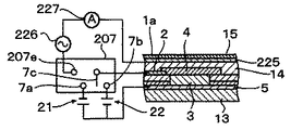
図1はこの発明の第1の実施形態に係るタッチ式入力装置の分解斜視図、図2は図1のII−II線に沿う断面図、図3は図1に示すタッチ式入力装置の電解質保持層の平面図、図4は図1に示すタッチ式入力装置の表面保護材の平面図、図5は図1に示すタッチ式入力装置の回路図、図6は図1に示すタッチ式入力装置のスイッチの概念図である。 1 is an exploded perspective view of a touch input device according to a first embodiment of the present invention, FIG. 2 is a sectional view taken along line II-II of FIG. 1, and FIG. 3 is an electrolyte of the touch input device shown in FIG. 4 is a plan view of the surface protective material of the touch input device shown in FIG. 1, FIG. 5 is a circuit diagram of the touch input device shown in FIG. 1, and FIG. 6 is a touch input shown in FIG. It is a conceptual diagram of the switch of an apparatus.
このタッチ式入力装置は例えばデジタルビデオカメラ(図示せず)の入力装置として好適であり、ビューワ(液晶モニタ)を収容するためにビデオカメラ本体の側面に形成された凹部に設けられる。 This touch-type input device is suitable as an input device for a digital video camera (not shown), for example, and is provided in a recess formed on the side surface of the video camera main body in order to accommodate a viewer (liquid crystal monitor).
図1に示すように、このタッチ式入力装置は複数の導体パターン(第1電極)2と複数の電解質層3と複数の導電性高分子層4と下部電極(第2電極)5と切替スイッチ(第1の電圧印加手段)7(図5参照)とを備える。
As shown in FIG. 1, the touch input device includes a plurality of conductor patterns (first electrodes) 2, a plurality of
導体パターン2は電解質保持層11の上面に形成されている。図3に示すように、電解質保持層11は複数の孔11aを有する。また、電解質保持層11は複数の導電性高分子形成エリア11bを有する。孔11aは導電性高分子形成エリア11b内に位置する。導電性高分子形成エリア11b内には導体パターン2の一端部が入り込んでいる(図3参照)。電解質保持層11として、PET(ポリエチレンテレフタレート)、ポリイミド、ポリカーボネイト等の絶縁性プラスチックシートを用いることができる。電解質保持層11は各種インクを用いても形成することができる。電解質保持層11は粘着材12によって下部電極5に貼着されている。粘着材12は孔11aに対応する孔12aを有している(図2参照)。
The
電解質層3は下部電極5上に形成され、孔11a,12a内に収容されている。電解質層3としては各種の電解質を使用することができるが、製造工程上の取扱が容易であり、室温でも高いイオン伝導率を示す高分子固体電解質を用いるのが望ましい。
The
高分子固体電解質としては、例えば、ホストポリマーと低分子有機可塑材と電解質塩とからなるものを使用することができる。 As the polymer solid electrolyte, for example, a polymer composed of a host polymer, a low molecular organic plasticizer, and an electrolyte salt can be used.
ホストポリマーとしては、ポリエチレンオキシド、ポリプロピレンオキシド、ポリアクリロニトリル、ポリピニリデンオロライド等を使用することができる。 Examples of the host polymer that can be used include polyethylene oxide, polypropylene oxide, polyacrylonitrile, and polypinylideneolide.
低分子有機可塑材としては、エチレンカーボネート、プロピレンカーボネート、ジメチルカーボネート、テトラヒドロフラン、ジメトキシエタン等を使用することができる。 As the low molecular organic plasticizer, ethylene carbonate, propylene carbonate, dimethyl carbonate, tetrahydrofuran, dimethoxyethane and the like can be used.
電解質塩としては、LiClO4,LiBF4,LiPF6,LiAsF6,LiCF3SO3,LiN(CF3SO2)2 等を使用することができる。 As the electrolyte salt, LiClO4, LiBF4, LiPF6, LiAsF6, LiCF3SO3, LiN (CF3SO2) 2 or the like can be used.
導電性高分子層4は電解質保持層11の上面の導電性高分子形成エリア11bに設けられている。したがって、導電性高分子層4の一部分は導体パターン2の一端部に重なり、導体パターン2に接続される。
The
導電性高分子は電子を奪ったり、与えたりする働きを有するドーパントを高分子にドーピングすることによって得られる。 A conductive polymer can be obtained by doping a polymer with a dopant having the function of depriving or giving electrons.
導電性高分子に用いられる主な高分子としては、ポリピロール、ポリアニリン、ポリチオフェン及びこれらの主鎖をアルキル基で修飾した誘導体並びにポリアセチレン、ポリパラフェニレンビニリデンといったものが知られている。 As main polymers used for the conductive polymer, polypyrrole, polyaniline, polythiophene, derivatives obtained by modifying these main chains with alkyl groups, polyacetylene, polyparaphenylene vinylidene, and the like are known.
また、導電性高分子に用いられる主なドーパントとしては、リチウム等のアルカリ金属、臭素等のハロゲン類、塩酸等のプロトン酸、アルキルベンゼンスルホン酸塩等の界面活性剤等が知られている。 As main dopants used for the conductive polymer, alkali metals such as lithium, halogens such as bromine, proton acids such as hydrochloric acid, surfactants such as alkylbenzene sulfonate, and the like are known.
第1の実施形態の導電性高分子層4を構成する導電性高分子は、単結合と2重結合とが交互に現れる共役2重結合の繰り返し構造を有する高分子に、電子を与えるドーパントをドーピングしたものであり、自由に移動できるπ電子を有する。
The conductive polymer constituting the
因みに、導電性高分子は電気化学的な酸化還元反応によって伸縮運動をすることが知られている。 Incidentally, it is known that a conductive polymer expands and contracts by an electrochemical redox reaction.
この現象は、導電性高分子の周囲にイオン供給源となる電解質が存在する環境で導電性高分子の酸化還元反応が起きると、電解質中のイオンが導電性高分子に吸収されたり、排出されたりしてイオン体積分だけ導電性高分子の体積が変化することによって生じるか、或いは高分子類のコンフォメーション変化や分子間/分子内の静電反発によって生じる。 This phenomenon is caused when the conductive polymer undergoes an oxidation-reduction reaction in an environment where there is an electrolyte serving as an ion source around the conductive polymer, and the ions in the electrolyte are absorbed or discharged by the conductive polymer. For example, it is caused by a change in the volume of the conductive polymer by the ionic volume, or by a change in the conformation of polymers or an electrostatic repulsion between molecules / molecules.
導電性高分子の伸縮運動は数ボルトといった低電圧で起こり、低電圧でも220kg/cm2程度の応力が発生し、導電性高分子の厚さを約15%の増加させることができる。
The expansion and contraction motion of the conductive polymer occurs at a low voltage of several volts. Even at a low voltage, a stress of about 220 kg /
また、導電性高分子に圧力をかけると、導電性高分子内のフィブリル間の距離、相互作用が変化し、また、主鎖間の距離、相互作用が変化して導電性高分子の導電率が変化する。この性質を利用して導電性高分子に圧力が加わったか否か、また、どの程度の圧力が加わったかを検出することができる。 In addition, when pressure is applied to the conductive polymer, the distance and interaction between the fibrils in the conductive polymer change, and the distance between the main chains and the interaction also change, and the conductivity of the conductive polymer changes. Changes. Using this property, it is possible to detect whether and how much pressure is applied to the conductive polymer.
下部電極5は基板13の上面全体に形成されている。基板13としては、PET、アクリル、ABS(アクリロニトリル ブタジエン スチレン樹脂)、ガラス等の薄板を用いることができる。
The
電解質保持層11及び導電性高分子層4の上面には粘着材14を介して表面保護材15が貼着されている。表面保護材15には、図4に示すように、入力ボタンとして各導電性高分子層4が受け持つ機能を表わす表示15aが描かれている。表面保護材15としては、天然ゴム、ポリウレタン、ウレタンフォーム等のエラストマのシート、薄型PET、薄型ポリカーボネート、薄型ポリイミド等を使用することができる。
A surface
基材13の下面には粘着材16を介して検出パネル17が貼着されている。この検出パネル17はどの導電性高分子層4が押圧されたかを検出するものである。検出パネル17としては、抵抗膜式、感圧ゴムを使用した感圧式等のタッチパネル、メンブレンスイッチ等を使用することができる。
A
図5に示すように、切替スイッチ7は第1固定接点7a、第2固定接点7b,可動接点7cを有している。第1固定接点7aは第1直流電源21の負極側端子21bに接続されている。第1直流電源21の陽極側端子21aは下部電極5に接続されている。第2固定接点7bは第2直流電源22の陽極側端子22aに接続されている。第2直流電源22の陰極側端子22bは下部電極5に接続されている。切替スイッチ7には、可動接点7cが第1固定接点7aに接触するか、第2固定接点7bに接触するか、或いはいずれの固定接点7a,7bにも接触しないかの3つの態様がある。可動接点7cには、スイッチ18,18´が並列に接続されている。スイッチ18は導体パターン2を介して図5の左側2列の導電性高分子層4−1〜8に接続されている。スイッチ18´は導体パターン2を介して図5の右側2列の導電性高分子層4−9〜16に接続されている。図6に示すように、スイッチ18は複数の固定接点18aと複数の可動接点18bとを有する。固定接点18aの数は図5の左側2列の導電性高分子層4の数と同じである。これらの固定接点18aは可動接点7cに並列に接続されている。可動接点18bの数は固定接点18aの数と同じである。スイッチ18には、可動接点18bが固定接点18aに接触するか或いは接触しないかの2つの態様がある。スイッチ18´はスイッチ18と同じ構成である。
As shown in FIG. 5, the
次に、このタッチ式入力装置の組立手順について説明する。 Next, the assembly procedure of this touch type input device will be described.
まず、孔11aが形成された電解質保持層11の上面に銀ペースト、カーボンペースト等の導電性ペーストを印刷して導体パターン2を形成する。この方法以外に、電解質保持層11の導体パターン2が形成される部分を除いてマスクし、その後、ITO(Indium
Tin Oxide)等を電解質保持層11に蒸着することによっても導体パターン2を形成することができる。
First, a
The
また、基板13の上面全体に銀ペースト、カーボンペースト等の導電性ペーストを印刷して下部電極5を形成する。この方法以外に、ITO等を基板13の上面に蒸着することによっても下部電極5を形成することができる。
Further, the
次に、電解質保持層11の下面に粘着材12を印刷する。このとき、孔12aを形成する。電解質保持層11の下面に印刷した粘着材12によって下部電極5上に電解質保持層11を貼着する。
Next, the
その後、ホストポリマー、低分子有機可塑材及び電解質塩の混合物を印刷技術を用いて孔11a,12a内に充填する。そして、この混合物を加熱して高分子固体電解質層3を形成する。
Thereafter, a mixture of the host polymer, the low molecular organic plastic material and the electrolyte salt is filled into the
次に、導電性高分子形成エリア11bを除いて電解質保持層11の上面をマスクし、導電性高分子形成エリア11b上に導電性高分子層4としてポリピロールを形成した。このポリピロールのドーパントはドデシルベンゼンスルホン酸とした。
Next, the upper surface of the
その後、電解質保持層11上のマスクを外し、電解質保持層11及び導電性高分子層4の上面に粘着材14を印刷し、その上に表面保護材15を貼着する。
Thereafter, the mask on the
最後に、上述の工程により得られた積層体を粘着材16を介して検出パネル17に貼着する。
Finally, the laminate obtained by the above-described process is attached to the
以上の工程により第1の実施形態のタッチ式入力装置が組み立てられる。 The touch input device of the first embodiment is assembled by the above steps.
図7は図1に示すタッチ式入力装置の動作を説明するための図であって、図7Aは初期状態の斜視図、図7Bは入力待機状態の斜視図、図7Cは再生ボタンを押下した状態の斜視図、図7Dはリセット状態の斜視図、図7Eは限定的入力待機状態の斜視図、図7Fは停止ボタンを押下した状態の斜視図、図7Gはリセット状態の斜視図、図7Hは入力待機状態の斜視図、図7Iは初期状態の斜視図である。 7 is a diagram for explaining the operation of the touch-type input device shown in FIG. 1. FIG. 7A is a perspective view in an initial state, FIG. 7B is a perspective view in an input standby state, and FIG. 7D is a perspective view in a reset state, FIG. 7E is a perspective view in a limited input standby state, FIG. 7F is a perspective view in a state where a stop button is pressed, FIG. 7G is a perspective view in a reset state, and FIG. Is a perspective view in an input standby state, and FIG. 7I is a perspective view in an initial state.
デジタルビデオカメラには、ビューワを開くと、ビューワ収納部内に多数の操作ボタンが現われ、録画した画像の再生、スロー再生、早送り、巻戻し、停止、一時停止等の操作や各種の設定操作をできるものがある。 When a viewer is opened on a digital video camera, a number of operation buttons appear in the viewer compartment, allowing you to perform operations such as playback, slow playback, fast forward, rewind, stop, pause, and various settings for recorded images. There is something.
例えば、早送りの操作を行った後、次に操作するのは再生、スロー再生、巻戻し、停止或いは一時停止の操作ボタンである可能性が高く、設定用の操作ボタンを操作する可能性は極めて低いし、設定用操作ボタンはブラインドタッチの操作を行う上で障害になる。 For example, after performing a fast-forward operation, it is highly likely that the next operation will be a play, slow play, rewind, stop or pause operation button, and the possibility of operating the setting operation button is extremely high The operation button for setting is an obstacle to the blind touch operation.
以下、第1の実施形態のタッチ式入力装置の基本的な動作を説明する。 The basic operation of the touch input device according to the first embodiment will be described below.
デジタルビデオカメラのビューワが開いていないとき、図7Aに示すように、タッチ式入力装置1の入力面1aは平坦である。
When the viewer of the digital video camera is not open, the
ビューワを開くと、全ての導電性高分子層4−1〜16(図5参照)が膨張して、図7Bに示すように、全ての操作ボタン10−1〜16(ハイフォン以下の符号は導電性高分子層4−1〜16との対応関係を示す)が隆起する。 When the viewer is opened, all the conductive polymer layers 4-1 to 16-16 (see FIG. 5) are expanded, and as shown in FIG. The corresponding relationship with the conductive polymer layers 4-1 to 16) is raised.
操作ボタン(再生ボタン)10−2を押すと、再生ボタン10−2に対応する導電性高分子層4−2が収縮し、図7Cに示すように、再生ボタン10−2が引っ込む。 When the operation button (play button) 10-2 is pressed, the conductive polymer layer 4-2 corresponding to the play button 10-2 contracts, and the play button 10-2 is retracted as shown in FIG. 7C.
その後、図7Dに示すように、全ての操作ボタン10−1〜16が一旦引っ込み、直ぐに、図7Eに示すように、再生ボタン10−2に密接に関連する操作ボタン10−1,3〜8が隆起する。 Thereafter, as shown in FIG. 7D, all the operation buttons 10-1 to 10-16 are temporarily retracted, and immediately, as shown in FIG. 7E, the operation buttons 10-1, 3-8 closely related to the reproduction button 10-2. Rises.
操作ボタン(停止ボタン)10−6を押すと、停止ボタン10−6に対応する導電性高分子層4−6が収縮し、図7Fに示すように、停止ボタン10−6が引っ込む。 When the operation button (stop button) 10-6 is pressed, the conductive polymer layer 4-6 corresponding to the stop button 10-6 contracts, and the stop button 10-6 is retracted as shown in FIG. 7F.
停止ボタン10−6を操作した後は全ての操作ボタン10−1〜16が操作される可能性があるので、図7Gに示すように、全ての操作ボタン10−1〜16が一旦引っ込み、直ぐに図7Hに示すように、全ての操作ボタン10−1〜16が隆起する。 Since all the operation buttons 10-1 to 16-16 may be operated after the stop button 10-6 is operated, as shown in FIG. 7G, all the operation buttons 10-1 to 16-16 are temporarily retracted and immediately As shown in FIG. 7H, all the operation buttons 10-1 to 16-16 are raised.
ビューワを閉じると、全ての導電性高分子層4−1〜16が収縮して、図7Iに示すように、全ての操作ボタン10−1〜16が引っ込む。 When the viewer is closed, all the conductive polymer layers 4-1 to 16-16 contract and all the operation buttons 10-1 to 16-16 retract as shown in FIG. 7I.
図8は図1に示すタッチ式入力装置の制御系を示すブロック図、図9は図1に示すタッチ式入力装置の動作を説明するための図であって、図9Aは初期状態の断面図、図9Bは凸形成状態の断面図、図9Cは凸保持状態の断面図、図9Dは凸解除状態の断面図、図9Eは初期状態の断面図である。 8 is a block diagram showing a control system of the touch input device shown in FIG. 1, FIG. 9 is a diagram for explaining the operation of the touch input device shown in FIG. 1, and FIG. 9A is a sectional view in an initial state. 9B is a cross-sectional view in a convex formation state, FIG. 9C is a cross-sectional view in a convex holding state, FIG. 9D is a cross-sectional view in a convex release state, and FIG. 9E is a cross-sectional view in an initial state.
図8に示すように、第1の実施形態のタッチ式入力装置は制御部20と切替スイッチ7とスイッチ18,18´と検出パネル17と検出スイッチ23とを備えている。
As shown in FIG. 8, the touch input device according to the first embodiment includes a
ビューワを開き、その後デジタルビデオカメラの電源を入れるか、或いは電源がONの状態でビューワを開くと、検出スイッチ23はビューワが開いたことを検出し、その検出信号SG1を制御部20へ送る。このとき、切替スイッチ7は図9Aに示す状態になっている。
When the viewer is opened and then the digital video camera is turned on, or when the viewer is opened with the power turned on, the
制御部20はこの検出信号SG1を受け取ると、スイッチ18,18´に対して全ての導電性高分子層4に通電できるように全ての可動接点18b(図6参照)を閉じる制御信号SG2を送る。
Upon receiving this detection signal SG1, the
これと同時に、制御部20は切替スイッチ7に対して導電性高分子層4を第1直流電源21の陰極に、下部電極5を第1直流電源21の陽極に接続するように可動接点7cを切り替える制御信号SG3を送る。この結果、可動接点7cは図9Bに示す状態になる。これにより、導電性高分子層4に電解質層3中のカチオンがドープされ、導電性高分子層4の体積が増える。この結果、表面保護材15の一部分が凸状に盛上り、操作ボタン10が出現する。
At the same time, the
切替スイッチ7の可動接点7cが図9Bの状態になってから所定時間(導電性高分子層4が膨張するのに要する時間)経過後、制御部20は切替スイッチ7に対して可動接点7cを開く制御信号SG4を送る。この結果、図9Cの状態になる。この状態では、導電性高分子層4の膨張が止まり、導電性高分子層4はそのままの形状を保つ。したがって、表面保護部材15にできた操作ボタン10は凸状態を維持する。その凸状態を維持するための電力は不要である。この図9Cの状態は操作ボタン10の入力待機状態である。
After a predetermined time (time required for the
操作者が再生ボタン10−2を押すと、検出パネル17は再生ボタン10−2が押圧されたことを検出し、検出信号SG5を制御部20に送る。
When the operator presses the playback button 10-2, the
この検出信号SG5を制御部20が受け取ると、制御部20はビデオを再生する処理を行う。
When the
これと同時に制御部20はスイッチ18,18´に対して再生ボタン10−2に対応する導電性高分子層4−2にだけ通電できるように可動接点18bを切り替える制御信号SG6を送る。
At the same time, the
また、制御部20は切替スイッチ7に対して導電性高分子層4を第2直流電源22の陽極に、下部電極5を第2直流電源22の陰極に接続するように可動接点7cを切り替える制御信号SG7を送る。これにより、導電性高分子層4にドープされていたカチオンが脱ドープされ、導電性高分子層4の体積が減り、図9Dの状態になる。
Further, the
この結果、再生ボタン10−2だけが引っ込み、それ以外の操作ボタン10−1,3〜16は凸状態を保つ(図7Cの状態)。 As a result, only the reproduction button 10-2 is retracted, and the other operation buttons 10-1, 3 to 16 are kept in a convex state (the state shown in FIG. 7C).
切替スイッチ7の可動接点7cが図9Dの状態になってから所定時間(導電性高分子層4が収縮するのに要する時間)経過後、制御部20は切替スイッチ7に対して可動接点7cを開く制御信号SG8を送る。この結果、図9Eの状態になる。
After a predetermined time (time required for the
再生ボタン10−2が押圧されてから所定時間経過(例えば1秒以内の短時間が望ましい)すると、制御部20はスイッチ18,18´に対して再生ボタン10−2に対応する導電性高分子層4−2以外の全ての導電性高分子層4−1,3〜16に通電できるように可動接点18bを切り替える制御信号を送る。
When a predetermined time elapses after the playback button 10-2 is pressed (for example, a short time within 1 second is desirable), the
これと同時に、制御部20は切替スイッチ7に対して導電性高分子層4を第2直流電源22の陽極に、下部電極5を第2直流電源22の陰極に接続するように可動接点7cを切り替える制御信号を送る(図9Dに示す状態)。これにより、全ての導電性高分子層4の体積が減る。この結果、全ての操作ボタン10−1〜16が引っ込む(図7Dの状態)。
At the same time, the
切替スイッチ7の可動接点7cが図9Dの状態になってから所定時間経過後、制御部20は切替スイッチ7に対して可動接点7cを開く制御信号を送る(図9Aの状態)。
After a predetermined time has elapsed since the
その直後に、制御部20はスイッチ18,18´に対して再生ボタン10−2に関連する操作ボタン10−1,3〜8を形作る導電性高分子層4−1,3〜8にだけ通電できるように可動接点18bを切り替える制御信号を送る。
Immediately thereafter, the
また、制御部20は切替スイッチ7に対して導電性高分子層4を第1直流電源21の陰極に、下部電極5を第1直流電源21の陽極に接続するように可動接点7cを切り替える制御信号を送る(図9Bの状態)。この結果、再生ボタン10−2に関連する操作ボタン10−1,3〜8だけが出現する(図7Eの状態)。
Further, the
制御部20が可動接点7cを切り替える制御信号を出力してから所定時間経過後、制御部20は切替スイッチ7に対して可動接点7cを開く制御信号を送る(図9Cの状態)。
After a predetermined time elapses after the
操作者が停止ボタン10−6を押すと、検出パネル17は停止ボタン10−6が押圧されたことを検出し、検出信号を制御部20に送る。
When the operator presses the stop button 10-6, the
この検出信号を制御部20が受け取ると、制御部20はビデオを停止する処理を行う。
When the
これと並行して制御部20は再生ボタン10−2が押されたときの制御と同様の制御を行って停止ボタン10−6を引っ込める(図7Fの状態)。
In parallel with this, the
停止ボタン10−6を操作した後は全ての操作ボタン10−1〜16が操作対象となるので、制御部20は停止の処理を行った後に、一旦凸状になっている全ての操作ボタン10−1〜16を引っ込め(図7Gの状態)、更に、全ての操作ボタン10−1〜16を出現させる(図7Hの状態)。
After the stop button 10-6 is operated, all the operation buttons 10-1 to 10-16 are to be operated. Therefore, after the
凸状になっている全ての操作ボタン10−1〜16を引っ込める制御は、再生ボタン10−2を押圧した後で、凸状になっている全ての操作ボタン10−1〜16を引っ込める制御と同様である。 The control for retracting all the operation buttons 10-1 to 16-16 having a convex shape is a control for retracting all the operation buttons 10-1 to 16 having a convex shape after pressing the reproduction button 10-2. It is the same.
また、全ての操作ボタン10−1〜16を出現させる制御は、ビューワを開いたときに全ての操作ボタン10−1〜16を出現させる制御と同様である。 Further, the control for causing all the operation buttons 10-1 to 16 to appear is the same as the control for causing all the operation buttons 10-1 to 16 to appear when the viewer is opened.
ビューワを閉じると、検出スイッチ23はビューワが閉じたことを検出し、その検出信号を制御部20へ送る。
When the viewer is closed, the
制御部20はこの検出信号を受け取ると、スイッチ18,18´に対して全ての導電性高分子層4に通電できるように全ての可動接点18bを閉じる制御信号を送る。
Upon receiving this detection signal, the
また、制御部20は切替スイッチ7に対して導電性高分子層4を第2直流電源22の陽極に、下部電極5を第2直流電源22の陰極に接続するように可動接点7cを切り替える制御信号を送る。この結果、全ての導電性高分子層4の体積が減り、全ての操作ボタン10が引っ込む(図9Dの状態)。
Further, the
その後、制御部20は切替スイッチ7に対して可動接点7cを開く制御信号を送る(図9Eの状態)。この結果、タッチ式入力装置1は初期状態に戻る(図9Aの状態)。
Then, the
次に、第1の実施形態のタッチ式入力装置の操作感について説明する。 Next, the operational feeling of the touch input device according to the first embodiment will be described.
図10はタッチ式入力装置の操作時に時間の経過とともに変化する操作者の指に加わる反力と時間の経過とともに変化する操作ボタンの高さとを示すグラフである。 FIG. 10 is a graph showing the reaction force applied to the operator's finger that changes with time during the operation of the touch input device and the height of the operation button that changes with time.
図10において、時間tの原点0は入力待機状態から操作者が操作ボタン10を押し始めた時点である。操作ボタン10の高さxの変化は入力待機状態からの変化とした。
In FIG. 10, the
図10に示す(1)の段階では切替スイッチ7はオフになっており、操作ボタン10は凸状態を保つ。このため、操作ボタン10を押圧しても操作ボタン10の高さxは変化せず、また、指に加わる反力Fは単調に増加する。
In the stage (1) shown in FIG. 10, the
図10に示す(2)の段階は操作ボタン10が押圧されたことを検出パネル17が検知し、制御部20が導電性高分子層4を第2直流電源22の陽極に、下部電極5を第2直流電源22の陰極に接続するように切替スイッチ7を制御した段階である。この段階では操作ボタン10の高さxは急に低くなり、指に加わる反力Fは小さくなる。
In the step (2) shown in FIG. 10, the
図10に示す(3)の段階では切替スイッチ7はオフになっているため、操作ボタン10は初期状態(操作ボタン10の高さxが0の状態)を保ち、指に加わる反力Fは単調に増加する。
Since the
図10に示すF−t特性は一般的な押しボタンの操作感を示すF−t特性と似ており、一般的な機械式の押しボタンスイッチと同様の操作感が得られることが分かる。 The Ft characteristic shown in FIG. 10 is similar to the Ft characteristic indicating the operation feeling of a general push button, and it can be seen that the same operation feeling as that of a general mechanical push button switch can be obtained.
図11は図1に示すタッチ式入力装置の基本的動作を説明するためのフローチャート図である。 FIG. 11 is a flowchart for explaining the basic operation of the touch input device shown in FIG.
タッチ式入力装置1が操作者に操作感を与えるまでの過程を図11を用いて説明する。
A process until the touch-
図11に示すように、操作ボタン10が所定の高さまで隆起したら、制御部20は導電性高分子層4及び下部電極5への通電を停止する(ステップS1)。これ以降は操作ボタン10の凸状態が保持され、操作ボタン10は入力待機状態になる。
As shown in FIG. 11, when the
次に、操作ボタン10を押し、入力(加圧)する(ステップS2;ステップS1〜S2の状態が図10の(1)の段階である)。
Next, the
検出パネル17はどの操作ボタン10が押されたかを検出し、その検出信号を制御部20へ送る(ステップS3)。
The
この検出信号を制御部20が受け取ると、制御部20は押圧された操作ボタン10を形作る導電性高分子層4を収縮するように導電性高分子層4及び下部電極5に通電する(ステップS4)。
When the
その結果、操作ボタン10が引っ込む。このとき、指先を通じて操作感が得られる(ステップS5;ステップS3〜S5が図10の(2)の段階である)。
As a result, the
以上のように、第1の実施形態によれば、操作者は機械式の押しボタンを押下したときと同様の操作感を得ることができるとともに、操作性を高めることができる。 As described above, according to the first embodiment, the operator can obtain the same operational feeling as when pressing a mechanical push button and can improve operability.
次に、第1の実施形態の変形例について説明する。 Next, a modification of the first embodiment will be described.
図12は第1の実施形態の変形例に係るタッチ式入力装置の回路図、図13は導体パターンと下部電極とに交流電源を印加したときの操作ボタンの高さの変化を示すグラフである。 FIG. 12 is a circuit diagram of a touch input device according to a modification of the first embodiment, and FIG. 13 is a graph showing a change in height of the operation button when AC power is applied to the conductor pattern and the lower electrode. .
この変形例は第1の実施形態とほぼ同じ構成であるので、構成の同じ部分については第1の実施形態と同じ符号を付してその説明を省略し、構成の異なる部分についてだけ説明する。 Since this modified example has almost the same configuration as that of the first embodiment, the same components as those in the first embodiment are denoted by the same reference numerals as those in the first embodiment, and the description thereof will be omitted. Only the components having different configurations will be described.
この変形例に係るタッチ式入力装置の切替スイッチ(第1の電圧印加手段と第2の電圧印加手段とを兼ねる)107は第3固定接点107dを有する。第3固定接点107dは交流電源124を介して下部電極5に接続されている。切替スイッチ107には、可動接点7cが第1固定接点7aに接触するか、第2固定接触点7bに接触するか、第3固定接点107dに接触するか、或いはいずれの固定接点7a,7b,107dにも接触しないかの4つの態様がある。
The changeover switch (also serving as the first voltage application unit and the second voltage application unit) 107 of the touch input device according to this modification has a third
可動接点7cが第3固定接点107dに接触すると、導体パターン2と下部電極5との間に交流電圧が印加される。この結果、導電性高分子層4は膨張、収縮を繰り返すので、操作ボタン10の高さxは図13に示すように変化する。すなわち、操作ボタン10は振動する。
When the
この第1の実施形態の変形例によれば、第1の実施形態と同様の効果を奏するとともに、操作ボタン10が振動することによって、入力操作領域とそれ以外の領域とを容易に識別することができる。
According to the modification of the first embodiment, the same effect as that of the first embodiment can be obtained, and the input operation area and the other areas can be easily identified by vibrating the
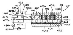
図14はこの発明の第2の実施形態に係るタッチ式入力装置の分解斜視図、図15は図14のXV-XV に沿う断面図、図16は図14に示すタッチ式入力装置の電解質保持層の平面図、図17は図14に示すタッチ式入力装置の回路図である。 14 is an exploded perspective view of the touch input device according to the second embodiment of the present invention, FIG. 15 is a sectional view taken along XV-XV in FIG. 14, and FIG. 16 is an electrolyte holding device of the touch input device shown in FIG. FIG. 17 is a circuit diagram of the touch-type input device shown in FIG.
この第2の実施形態は第1の実施形態とほぼ同じ構成であるので、構成の同じ部分については第1の実施形態と同じ符号を付してその説明を省略し、構成の異なる部分についてだけ説明する。 Since the second embodiment has substantially the same configuration as the first embodiment, the same parts as those in the first embodiment are denoted by the same reference numerals as those in the first embodiment, and the description thereof is omitted. explain.
図14〜17に示すように、第2の実施形態のタッチ式入力装置201では、表面保護層15の下面に上部電極(第3電極)225が形成されている。
As shown in FIGS. 14 to 17, in the
また、第2の実施形態では、第1の実施形態で採用された検出パネル17が削除されている。
In the second embodiment, the
図17に示すように、第2の実施形態では切替スイッチ207(第1の電圧印加手段と第3の電圧印加手段とを兼ねる)は第3固定接点207eを有する。第3固定接点207eは交流電源226を介して上部電極225に接続されている。切替スイッチ207には、可動接点7cが第1固定接点7aに接触するか、第2固定接触点7bに接触するか、第3固定接点207eに接触するか、或いはいずれの固定接点7a,7b,207eにも接触しないかの4つの態様がある。
As shown in FIG. 17, in the second embodiment, the changeover switch 207 (which serves as both the first voltage application unit and the third voltage application unit) has a third
図18は図14に示すタッチ式入力装置の上層部の等価回路図、図19は図14に示すタッチ式入力装置の制御系のブロック図、図20は図14に示すタッチ式入力装置の動作を説明するための図であって、図20Aは初期状態の断面図、図20Bは凸形成状態の断面図、図20Cは凸保持状態の断面図、図20Dは凸解除状態の断面図、図20Eは初期状態の断面図である。 18 is an equivalent circuit diagram of the upper layer portion of the touch input device shown in FIG. 14, FIG. 19 is a block diagram of a control system of the touch input device shown in FIG. 14, and FIG. 20 is an operation of the touch input device shown in FIG. 20A is a sectional view in an initial state, FIG. 20B is a sectional view in a convex formation state, FIG. 20C is a sectional view in a convex holding state, and FIG. 20D is a sectional view in a convex release state. 20E is a sectional view of the initial state.
図19に示すように、第2の実施形態のタッチ式入力装置は制御部20と切替スイッチ207とスイッチ18,18´と検出部227と検出スイッチ23とを備えている。
As shown in FIG. 19, the touch input device according to the second embodiment includes a
図18に示すように、検出部227は導体パターン2と上部電極225との間に流れる交流電流の値を測定し、検出信号を出力する電流計である。
As shown in FIG. 18, the
この第2の実施形態の制御は第1の実施形態の制御とほぼ同じであり、第1の実施形態ではタッチパネル等の専用の検出パネル17を用いていずれの操作ボタン10が押圧されたのかを検知するが、第2の実施形態では押圧された操作ボタン10を形作っている導電性高分子層4の導電率を検出して押圧された操作ボタン10を検知する。
The control of the second embodiment is almost the same as the control of the first embodiment. In the first embodiment, which
以下、第2の実施形態のタッチ式入力装置の動作を具体的に説明する。 The operation of the touch input device according to the second embodiment will be specifically described below.
ビューワが開き、操作ボタン10が出現するまで、すなわち、図20A〜図20Bまでの制御は図9A〜図9Bまでの制御と同じである。
Until the viewer opens and the
切替スイッチ207の可動接点7cが図20Bの状態になってから所定時間経過後、制御部20は切替スイッチ207に対して可動接点7cを第3固定接点207eに接触させる制御信号を送る。この結果、図20Cの状態になる。この状態では、導電性高分子層4と下部電極5との間に電圧が印加されない。したがって、導電性高分子層4と電解質層3との間でイオンの授受が行われないので、操作ボタン10は振動することなく、凸状態を維持する。この図20Cの状態は操作ボタン10の入力待機状態である。
After a predetermined time has elapsed since the
操作者が操作ボタン10を押すと、押された操作ボタン10を形作る導電性高分子層4の導電率が変化し、導体パターン2、上部電極225間を流れる電流値が変化する。この導電率が変化した導電性高分子層4に接続されている検出部(電流計)227は電流値の変化を検出し、この検出信号を制御部20へ送る。
When the operator presses the
この検出信号を制御部20が受け取ると、制御部20は切替スイッチ207に対して導電性高分子層4を第2直流電源22の陽極に、下部電極5を第2直流電源22の陰極に接続するように可動接点7cを切り替える制御信号を送る。これにより、導電性高分子層4の体積が減り、押圧された操作ボタン10が引っ込み、図20Dの状態になる。
When the
切替スイッチ7の可動接点7cが図20Dの状態になってから所定時間経過後、制御部20は切替スイッチ207に対して可動接点7cを開く制御信号を送る。この結果、図20Eの状態になる。
After a predetermined time has elapsed since the
図21はタッチ式入力装置の制御部の動作を説明するためのフローチャート図である。 FIG. 21 is a flowchart for explaining the operation of the control unit of the touch input device.
図21に示すように、操作ボタン10が所定の高さまで隆起したら、制御部20は導電性高分子層4及び下部電極5への通電を停止する(ステップS1)。
As shown in FIG. 21, when the
次に、制御部20は導電性高分子層4と上部電極225との間に交流電圧を印加させる(ステップS2)。これ以降は操作ボタン10の凸状態が保持され、操作ボタン10は入力待機状態になる。
Next, the
次に、操作ボタン10を押し、入力(加圧)の操作を行う(ステップS3)。
Next, the
このとき、押圧された操作ボタン10を形作る導電性高分子層4の導電率が変化する(ステップS4)。この導電性高分子層4に接続された検出部227は電流値の変化を検出し、その検出信号を制御部20へ送る(ステップS5)。制御部20はどの検出部227から検出信号が送られてきたかを検出する(ステップS6)。その後、制御部20は押圧された操作ボタン10を形作る導電性高分子層4を収縮させるように導電性高分子層4及び下部電極5に通電する(ステップS7)。
At this time, the conductivity of the
その結果、操作ボタン10が引っ込む。このとき操作感が得られる(ステップS8)。
As a result, the
以上のように、第2の実施形態によれば、第1の実施形態と同様の効果を得られるだけでなく、専用の検出パネル17を削除することができる。
As described above, according to the second embodiment, not only the same effects as those of the first embodiment can be obtained, but also the
図22は第2の実施形態の変形例に係るタッチ式入力装置の回路図である。 FIG. 22 is a circuit diagram of a touch input device according to a modification of the second embodiment.
この変形例に係るタッチ式入力装置201´の切替スイッチ(第1の電圧印加手段と第2の電圧印加手段と第3の電圧印加手段とを兼ねる)207´は第4固定接点207dを有する。第4固定接点207dは交流電源224を介して下部電極5に接続されている。切替スイッチ207´には、可動接点7cが第1固定接点7aに接触するか、第2固定接触点7bに接触するか、第3固定接点207eと第4固定接点207dとに交互に接触するか、或いはいずれの固定接点7a,7b,207e,207dにも接触しないかの4つの態様がある。
A change-over switch (also serving as a first voltage application unit, a second voltage application unit, and a third voltage application unit) 207 ′ of the
タッチ式入力装置201´の操作ボタン(図示せず)が入力待機状態のときに制御部(図示せず)は可動接点7cを第3固定接点207eと第4固定接点207dとに交互に接触させる。したがって、操作ボタンは振動しながら入力待機状態が維持される。可動接点7cが第3固定接点207eに接触している時間と可動接点7cが第4固定接点207dに接触している時間とはいずれも極めて短時間であるが、可動接点7cが第4固定接点207dに接触している時間の方が可動接点7cが第3固定接点207eに接触している時間よりも長い。したがって、振動状態の断続によって生じる違和感を緩和することができる。
When an operation button (not shown) of the
この変形例によれば、第2の実施形態の効果を奏するとともに、操作ボタンが振動することによって、入力操作領域とそれ以外の領域とを簡単に識別することができる。 According to this modification, the effects of the second embodiment can be obtained, and the input operation area and other areas can be easily identified by the operation button vibrating.
図23はこの発明の第3の実施形態に係るタッチ式入力装置の分解斜視図、図24は図23のXXIV-XXIV 線に沿う断面図、図25は図23に示すタッチ式入力装置のシートの平面図、図26は図23に示すタッチ式入力装置の回路図である。 23 is an exploded perspective view of the touch input device according to the third embodiment of the present invention, FIG. 24 is a cross-sectional view taken along line XXIV-XXIV in FIG. 23, and FIG. 25 is a sheet of the touch input device shown in FIG. FIG. 26 is a circuit diagram of the touch input device shown in FIG.
図23に示すように、第3の実施形態のタッチ式入力装置301は第1の導体パターン(第1電極)302と複数の電解質層303と複数の第1の導電性高分子層304と第2の導体パターン(第2電極)305と複数の第2の導電性高分子層306と切替スイッチ(第1の電圧印加手段)307(図26参照)とを備える。
As shown in FIG. 23, the
第1の導体パターン302はシート331の上面に形成されている。シート331は、図25に示すように、複数の導電性高分子形成エリア331bを有する。導電性高分子形成エリア331b内には導体パターン302の一端部が入り込んでいる。シート331としては絶縁体であればよく、PET、ポリカーボネート、ポリイミド等のプラスチックフィルムを使用することができる。
The
第1の導電性高分子層304はシート331上面の導電性高分子形成エリア331b内に設けられている。したがって、第1の導電性高分子層304の一部分は第1の導体パターン302の一端部に重なり、第1の導体パターン302に接続される。
The first
第1の導電性高分子層304としては、ドデシルベンゼンスルホン酸イオンやアニオン性高分子等の比較的大きなアニオン(陰イオン)をドーパントに持つものが好ましい。第3の実施形態では第1の導電性高分子層304としてドデシルベンゼンスルホン酸イオンをドーパントに持つポリピロールを用いた。
The first
電解質層303は第1の導電性高分子層304上に形成されている。電解質層303としては第1の実施形態の電解質層3と同じものを用いることができる。
The
第2の導体パターン305は表面保護材315の下面に形成されている。表面保護材315としては、第1の実施形態の表面保護材15と同じものを用いることができる。
The
第2の導電性高分子層306は表面保護材315の下面に設けられている。第2の導電性高分子層306の一部分は第2の導体パターン305の一端部に重なり、第2の導体パターン305に接続される。
The second
第2の導電性高分子層306としては、塩化物イオン等の比較的小さなアニオン(陰イオン)をドーパントに持つものが好ましい。第3の実施形態では第2の導電性高分子層306として塩化物イオンをドーパントに持つポリピロールを用いた。
The second
シート331の上面には粘着材332が印刷されている。図24に示すように、粘着材332が印刷されるとき、第1及び第2の導電性高分子層304,306並びに電解質層303を収容する孔332aが形成される。この粘着材332によって第2の導電性高分子層306及び導体パターン305が形成された表面保護材315がシート331に貼着される。
An
シート331の下面に粘着材333を介して検出パネル17が貼着されている。
The
図26に示すように、切替スイッチ307は第1固定接点307a、第2固定接点307b,可動接点307cを有している。第1固定接点307aは第1直流電源321の陰極側端子321bに接続されている。第1直流電源321の陽極側端子321aはスイッチ19,19´に並列に接続されている。スイッチ19,19´は第2の導体パターン305を介して第2導電性高分子層306に接続されている。第2固定接点307bは第2直流電源322の陽極側端子322aに接続されている。第2直流電源322の陰極側端子322bはスイッチ19,19´に並列に接続されている。切替スイッチ307には、可動接点307cが第1固定接点307aに接触するか、第2固定接点307bに接触するか、或いはいずれの固定接点307a,307bにも接触しないかの3つの態様がある。可動接点307cには、スイッチ18,18´が並列に接続されている。
As shown in FIG. 26, the
次に、このタッチ式入力装置の組立手順について説明する。 Next, the assembly procedure of this touch type input device will be described.
まず、シート331の上面に銀、カーボン、ITO、導電ゴム等で第1の導体パターン302を形成し、その後、導電性高分子形成エリア331b外の部分をマスクし、導電性高分子形成エリア331b内にポリピロールを形成し、これを第1の導電性高分子層304とする。第1の導電性高分子層304に含まれるドーパントとしてドデシルベンゼンスルホン酸を用いた。
First, the
次に、第1の導電性高分子層304上に電解質層303を形成する。電解質層303の形成方法は第1の実施形態の電解質層3の形成方法と同じである。
Next, the
その後、表面保護部材315の下面に第2の導体パターン305及び第2の導電性高分子層306を形成する。これらの形成方法は第1の導体パターン302及び第1の導電性高分子層304の形成方法と同様である。但し、第2の導電性高分子層306に含まれるドーパントとして塩化物イオンを用いた。
Thereafter, a
次に、粘着材332が第1及び第2の導電性高分子層304,306並びに電解質層303の周囲に形成されないようにマスクした後に、粘着材332をシート331上に塗布する。
Next, after masking the
その後、粘着材332上に表面保護材315を張る。表面保護材315を加圧すると、第2の導電性高分子層306と電解質層303とが接合される。
Thereafter, a surface
最後に、上述の工程によってシート331上に形成された積層体を粘着材333を介して検出パネル17の上面に貼着する。
Finally, the laminate formed on the
以上の工程により第3の実施形態のタッチ式入力装置が組み立てられる。 The touch input device of the third embodiment is assembled by the above steps.
図27は図23に示すタッチ式入力装置の制御系のブロック図、図28は図23に示すタッチ式入力装置の動作を説明するための図であって、図28Aは初期状態の断面図、図28Bは凸形成状態の断面図、図28Cは凸保持状態の断面図、図28Dは凸解除状態の断面図、図28Eは初期状態の断面図である。 27 is a block diagram of a control system of the touch input device shown in FIG. 23, FIG. 28 is a diagram for explaining the operation of the touch input device shown in FIG. 23, and FIG. 28A is a sectional view in an initial state, 28B is a cross-sectional view in the convex formation state, FIG. 28C is a cross-sectional view in the convex holding state, FIG. 28D is a cross-sectional view in the convex release state, and FIG. 28E is a cross-sectional view in the initial state.
図27に示すように、第3の実施形態のタッチ式入力装置は制御部20と切替スイッチ307とスイッチ18,18´,19,19´と検出パネル17と検出スイッチ23とを備えている。
As shown in FIG. 27, the touch-type input device of the third embodiment includes a
第1の実施形態では導体パターン2に接続された導電性高分子層4と、下部電極5との間に電圧を印加するのに対して、第3の実施形態では第1の導体パターン302と第2の導体パターン305とを通じて第1の導電性高分子層304と第2の導電性高分子層306との間に電圧を印加するようになっている。
In the first embodiment, a voltage is applied between the
また、第1の実施形態ではスイッチ18,18´は2つ設けられているが、第3の実施形態ではスイッチ18,18´,19,19´は4つ設けられている。この違いは第1の実施形態の導電性高分子層3は一層であるのに対して、第3の実施形態の導電性高分子層304,306は2層であることに起因する。第3の実施形態では、各層の導電性高分子層304,306を制御するために各層にスイッチ18,18´,19,19´を設ける必要がある。しかし、スイッチ19,19´はスイッチ18,18´と同じ構成であり、しかも、スイッチ19はスイッチ18と同じように動作でき、スイッチ19´はスイッチ18´と同じように動作できる。
In the first embodiment, two
以下、第3実施形態のタッチ式入力装置の動作を説明する。 Hereinafter, the operation of the touch input device according to the third embodiment will be described.
ビューワが開き、操作ボタン10が出現するまで、すなわち、図28A〜図28Bまでの制御は図9A〜図9Bまでの制御と同じである。
Until the viewer opens and the
図28Bに示すように、第1の導電性高分子層304を第1直流電源321の陰極に、第2の導電性高分子層306を第1直流電源321の陽極に接続するように切替スイッチ307が切り替えられると、第1の導電性高分子層304に電解質層303中のカチオンがドープされて第1の導電性高分子層304の体積が増加するとともに、第2の導電性高分子層306中に電解質層303のアニオンがドープされて第2の導電性高分子層306の体積が増加する。
As shown in FIG. 28B, the changeover switch is connected so that the first
切替スイッチ307の可動接点307cが図28Bの状態になってから所定時間経過後、制御部20は切替スイッチ307に対して可動接点307cを開く制御信号を送る。この結果、図28Cの状態になる。この状態では、第1の導電性高分子層304と第2の導電性高分子層電解質層306との間に電圧が印加されない。したがって、第1及び第2の導電性高分子層304,306と電解質層303との間でイオンの授受が行われないので、操作ボタン10は凸状態を維持する。
The
操作者が操作ボタン10を押すと、検出パネル17はどの操作ボタン10が押圧されたのかを検出し、この検出信号を制御部20に送る。
When the operator presses the
この検出信号を制御部20が受け取ると、制御部20は切替スイッチ307に対して第1の導電性高分子層304を第2直流電源322の陽極に、第2の導電性高分子層306を第2直流電源322の陰極とするように可動接点307cを切り替える制御信号を送る。これにより、第1の導電性高分子層304にドープされていたカチオンが脱ドープされて第1の導電性高分子層304の体積が減少するとともに、第2の導電性高分子層306中にドープされていたアニオンが脱ドープされて第2の導電性高分子層306の体積も減少する。この結果、第1及び第2の導電性高分子層304,306が収縮し、押圧された操作ボタン10が引っ込み、図28Dの状態になる。
When the
切替スイッチ307の可動接点307cが図28Dの状態になってから所定時間経過後、制御部20は切替スイッチ307に対して可動接点307cを開く制御信号を送る。この結果、図28Eの状態になる。
The
第3の実施形態によれば、第1の実施形態の効果を奏するとともに、2つの導電性高分子層304,306を用いるので、1つの導電性高分子層を用いるときに較べ全体としての変形量を増加させることができ、一層良好な操作感を得ることができる。また、1つの導電性高分子層の厚みを増やして変形量を増加させる方法に較べ変形の応答速度が低下しないので、この点でも一層良好な操作感を得ることができる。 According to the third embodiment, since the two conductive polymer layers 304 and 306 are used as well as the effects of the first embodiment, the deformation as a whole is more than when one conductive polymer layer is used. The amount can be increased, and a better operational feeling can be obtained. Further, since the response speed of deformation does not decrease compared to the method of increasing the amount of deformation by increasing the thickness of one conductive polymer layer, a better operational feeling can be obtained in this respect as well.
次に、第3の実施形態の変形例について説明する。 Next, a modification of the third embodiment will be described.
図29は第3の実施形態の第1の変形例に係るタッチ式入力装置の回路図である。 FIG. 29 is a circuit diagram of a touch input device according to a first modification of the third embodiment.
この変形例は第3の実施形態とほぼ同じ構成であるので、構成の同じ部分については第3の実施形態と同じ符号を付してその説明を省略し、構成の異なる部分についてだけ説明する。 Since this modification has almost the same configuration as that of the third embodiment, the same reference numerals as those of the third embodiment are assigned to the same components, and the description thereof is omitted, and only the components having different configurations will be described.
この変形例に係るタッチ式入力装置301´では、検出パネル17が削除され、その代わりに、図29に示すように、シート331の下面に下部電極(第3電極)335が形成された基板334(図32参照)が粘着材333によって貼着されている。
In the
また、この変形例に係るタッチ式入力装置301´の切替スイッチ(第1の電圧印加手段と第3の電圧印加手段とを兼ねる)307´は第3固定接点307eを有する。第3固定接点307eは交流電源326を介して下部電極335に接続されている。
In addition, the changeover switch (also serving as the first voltage applying unit and the third voltage applying unit) 307 ′ of the
図30は図29に示すタッチ式入力装置の制御系のブロック図、図31は図29に示すタッチ式入力装置の下層部の等価回路図、図32は図29に示すタッチ式入力装置の動作を説明するための図であって、図32Aは初期状態の断面図、図32Bは凸形成状態の断面図、図32Cは凸保持状態の断面図、図32Dは凸解除状態の断面図、図32Eは初期状態の断面図である。 30 is a block diagram of a control system of the touch input device shown in FIG. 29, FIG. 31 is an equivalent circuit diagram of a lower layer portion of the touch input device shown in FIG. 29, and FIG. 32 is an operation of the touch input device shown in FIG. 32A is a sectional view in an initial state, FIG. 32B is a sectional view in a convex formation state, FIG. 32C is a sectional view in a convex holding state, and FIG. 32D is a sectional view in a convex release state. 32E is a sectional view of the initial state.
図30に示すように、この変形例に係るタッチ式入力装置は制御部20と切替スイッチ307´とスイッチ18,18´,19,19´と検出部327と検出スイッチ23とを備えている。
As shown in FIG. 30, the touch input device according to this modification includes a
図31に示すように、検出部327は下部電極335と第1の導体パターン302との間に流れる交流電流の値を測定し、検出信号を出力する電流計である。
As shown in FIG. 31, the
この変形例の制御は第3の実施形態の制御とほぼ同じであり、違いは第3の実施形態では押圧された操作ボタン10を検知するのは検出専用の検出パネル17であるが、第3の実施形態の第1の変形例では押圧された操作ボタン10を形作っている第1の導電性高分子層304の導電率の変化を検出して押圧された操作ボタン10を検知する。
The control of this modification is almost the same as the control of the third embodiment. The difference is that in the third embodiment, the
以下、この変形例のタッチ式入力装置の動作を具体的に説明する。 Hereinafter, the operation of the touch input device of this modification will be specifically described.
ビューワが開き、操作ボタン10が出現するまで、すなわち、図32A〜図32Bまでの制御は図28A〜図28Bまでの制御と同じである。
The control from FIG. 32A to FIG. 32B is the same as the control from FIG. 28A to FIG. 28B until the viewer opens and the
切替スイッチ307´の可動接点307cが図32Bの状態になってから所定時間経過後、制御部20は切替スイッチ307´に対して可動接点307cを第3固定接点307eに接触させる制御信号を送る。この結果、図32Cの状態になる。この状態では、第1の導電性高分子層304と第2の導電性高分子層306との間に電圧が印加されない。したがって、第1及び第2の導電性高分子層304,306と電解質層303との間でイオンの授受が行われず、操作ボタン10は振動することなく、凸状態を維持する。この図32Cの状態は操作ボタン10の入力待機状態である。
After a predetermined time has elapsed since the
操作者が操作ボタン10を押すと、押された操作ボタン10を形作る第1の導電性高分子層304の導電率が変化し、下部電極335、導体パターン302間を流れる電流値が変化する。検出部(電流計)327は電流値の変化を検出し、この検出信号を制御部20へ送る。
When the operator presses the
この検出信号を制御部20が受け取ると、制御部20は切替スイッチ307´に対して第1の導電性高分子層304を第2直流電源322の陽極に、第2の導電性高分子層306を第2直流電源322の陰極に接続するに可動接点307cを切り替える制御信号を送る。これにより、第1の導電性高分子層304にドープされていたカチオンが脱ドープされて第1の導電性高分子層304の体積が減少するとともに第2の導電性高分子層306中にドープされていたアニオンが脱ドープされて第2の導電性高分子層306の体積も減少する。この結果、第1及び第2の導電性高分子層304,306が収縮し、押圧された操作ボタン10が引っ込み、図32Dの状態になる。
When the
切替スイッチ307´の可動接点307cが図32Dの状態になってから所定時間経過後、制御部20は切替スイッチ307´に対して可動接点307cを開く制御信号を送る。この結果、図32Eの状態になる。
After a predetermined time has elapsed since the
以上のように、第3の実施形態の変形例によれば、第3の実施形態と同様の効果を得られるだけでなく、専用の検出パネル17を削除することができる。
As described above, according to the modification of the third embodiment, not only the same effects as those of the third embodiment can be obtained, but also the
図33は第3の実施形態の第2の変形例に係るタッチ式入力装置の回路図である。 FIG. 33 is a circuit diagram of a touch input device according to a second modification of the third embodiment.
図33に示すように、この変形例は第1の変形例とほぼ同じ構成であるので、構成の同じ部分については第1の変形例と同じ符号を付してその説明を省略し、構成の異なる部分についてだけ説明する。 As shown in FIG. 33, this modified example has substantially the same configuration as the first modified example, and therefore, the same reference numerals as those in the first modified example are given to the same parts of the configuration, and the description thereof is omitted. Only the differences will be described.
この変形例に係るタッチ式入力装置301´´の切替スイッチ(第1の電圧印加手段とと第2の電圧印加手段と第3の電圧印加手段とを兼ねる)307´´は第4固定接点307dを有する。第4固定接点307dは交流電源324及びスイッチ19,19´を介して第2の導体パターン305に接続されている。
The
この変形例によれば、第3の実施形態の第1の変形例と同様の効果を得られるだけでなく、操作ボタンが振動することによって、入力操作領域とそれ以外の領域とを簡単に識別することができる。 According to this modified example, not only the same effect as the first modified example of the third embodiment can be obtained, but also the input operation region and other regions can be easily identified by the vibration of the operation button. can do.
図34はこの発明の第4の実施形態に係るタッチ式入力装置の断面図、図35は図34に示すタッチ式入力装置の導電性高分子層の平面図である。 34 is a cross-sectional view of a touch input device according to the fourth embodiment of the present invention, and FIG. 35 is a plan view of a conductive polymer layer of the touch input device shown in FIG.
図34、35に示すように、第4の実施形態のタッチ式入力装置401は導体パターン(第1電極)402と複数の電解質層403と複数の導電性高分子層404と上部電極(第2電極)405と切替スイッチ(第1及び第3の電圧印加手段)407(図36参照)とを備える。
As shown in FIGS. 34 and 35, the
導体パターン402はシート441の上面に形成されている。シート441は基板442の上面全体に形成された下部電極443に粘着材444を介して貼着されている。
The
導電性高分子層404はシート441上に形成され、導体パタンーン402に接続されている。導電性高分子層404には複数の孔404aが形成されている。
The
電解質層403は板状部403aと柱状部403bと側壁部403cとを有する。板状部403aは導電性高分子層404の上面に配置されている。柱状部403bは孔404aに収容されている。側壁部403cは板状部403aの周縁部に形成され、導電性高分子層404の周囲を覆っている。
The
上部電極405は表面保護材15の下面全体に形成されている。上部電極405はシート441上に印刷された粘着材445を介してシート441に貼着されている。
The
図36は図34に示すタッチ式入力装置の構成及び動作を説明するための図であって、図36Aは初期状態の断面図、図36Bは凸形成状態の断面図、図36Cは凸保持状態の断面図である。 36 is a diagram for explaining the configuration and operation of the touch-type input device shown in FIG. 34. FIG. 36A is a sectional view in an initial state, FIG. 36B is a sectional view in a convex formation state, and FIG. 36C is a convex holding state. FIG.
図36に示すように、第4の実施形態の切替スイッチ407は第2の実施形態の切替スイッチ207と同様のものであり、第1固定接点407a、第2固定接点407b、第3固定接点407e及び可動接点407cを有している。第1固定接点407aは第1直流電源421の陰極側端子421bに接続されている。第1直流電源421の陽極側端子421aは上部電極405に接続されている。第2固定接点407bは第2直流電源422の陽極側端子422aに接続されている。第2直流電源422の陰極側端子422bは上部電極405に接続されている。切替スイッチ407には、可動接点407cが第1固定接点407aに接触するか、第2固定接点407bに接触するか、固定接点407eに接触するか、或いはいずれの固定接点407a,407b,407eにも接触しないかの4つの態様がある。可動接点407cは、第2の実施形態のスイッチ18,18´と同様のスイッチ(図示せず)を介して導体パターン402に接続されている。
As shown in FIG. 36, the
第4の実施形態の動作は第2の実施形態とほぼ同じであるので、基本的な動作についてのみ説明する。 Since the operation of the fourth embodiment is almost the same as that of the second embodiment, only the basic operation will be described.
図36Aに示す初期状態から制御部(図示せず)が可動接点407cを第1固定接点407aに接触させるように切替スイッチ407を切り替えると、導電性高分子層404の体積が増え、図36Bに示す凸形成状態になる。
When the control unit (not shown) switches the
図36Bに示す凸形成状態になってから所定時間経過後、制御部(図示せず)は可動接点407cを第3接点407eに接触させるように切替スイッチ407を切り替える。この結果、タッチ式入力装置401は図36Cに示す凸保持状態になる。この状態は入力待機状態である。
After a predetermined time has elapsed since the convex formation state shown in FIG. 36B, the control unit (not shown) switches the
以上のように、第4の実施形態の初期状態体から凸保持状態までの動作は第2の実施形態の初期状態体から凸保持状態までの動作と同様であり、これ以外の第4の実施形態の動作も第2の実施形態の動作と同様である。 As described above, the operation from the initial state body to the convex holding state of the fourth embodiment is the same as the operation from the initial state body to the convex holding state of the second embodiment, and the fourth embodiment other than this. The operation of the embodiment is the same as that of the second embodiment.
第4の実施形態によれば、第2の実施形態と同様の効果を得られるだけでなく、導電性高分子層の厚みを増やして変形量を増加させたとしても、応答速度が低下しないので、一層良好な操作感を得ることができる。また、2つの導電性高分子層を用いて変形量を増加させる方法に較べ部品点数が少ないので、製造コストを低減することができる。 According to the fourth embodiment, not only can the same effect as the second embodiment be obtained, but even if the thickness of the conductive polymer layer is increased to increase the amount of deformation, the response speed does not decrease. A better operational feeling can be obtained. Moreover, since the number of parts is small compared to the method of increasing the amount of deformation using two conductive polymer layers, the manufacturing cost can be reduced.
図37は第4の実施形態の変形例に係るタッチ式入力装置の構成及び動作を説明するための図であって、図37Aは初期状態の断面図、図37Bは凸形成状態の断面図、図37Cは凸保持状態の断面図である。 FIG. 37 is a diagram for explaining the configuration and operation of a touch input device according to a modification of the fourth embodiment, in which FIG. 37A is a sectional view in an initial state, FIG. 37B is a sectional view in a convex formation state, FIG. 37C is a cross-sectional view of the convex holding state.
この変形例は第4の実施形態とほぼ同じ構成であるので、構成の同じ部分については第4の実施形態と同じ符号を付してその説明を省略し、構成の異なる部分についてだけ説明
この変形例に係るタッチ式入力装置401´の切替スイッチ(第1の電圧印加手段と第2の電圧印加手段と第3の電圧印加手段とを兼ねる)407´は第4固定接点407dを有する。第4固定接点407dは交流電源424を介して上部電極405に接続されている。
Since this modified example has almost the same configuration as that of the fourth embodiment, the same components as those of the fourth embodiment are denoted by the same reference numerals as those of the fourth embodiment, and the description thereof is omitted. Only the components having different configurations are described. The
この変形例によれば、第4の実施形態の効果を奏するとともに、操作ボタンが振動することによって、入力操作領域とそれ以外の領域とを簡単に識別することができる。 According to this modification, the effects of the fourth embodiment can be obtained, and the input operation area and other areas can be easily identified by the operation button vibrating.
第4の実施形態の他の変形例としては、下部電極443を形成した基板442を削除し、その代わりにシート441の下面に検出パネルを設けてもよい。
As another modification of the fourth embodiment, the
図38はこの発明の第5の実施形態に係るタッチ式入力装置の断面図、図39は図38に示すタッチ式入力装置の導電パターンの平面図である。 FIG. 38 is a sectional view of a touch input device according to the fifth embodiment of the present invention, and FIG. 39 is a plan view of a conductive pattern of the touch input device shown in FIG.
第5の実施形態は第2の実施形態とほぼ同じ構成であるので、構成の同じ部分については第2の実施形態と同じ符号を付してその説明を省略し、構成の異なる部分についてだけ説明する。 Since the fifth embodiment has almost the same configuration as the second embodiment, the same components as those of the second embodiment are denoted by the same reference numerals as those of the second embodiment, and the description thereof is omitted. Only the different components are described. To do.
図38、39に示すように、第5の実施形態のタッチ式入力装置501の導体パターン502は格子状部502aを有する。格子状部502aは導電性高分子層4の下面に埋め込まれている。
As shown in FIGS. 38 and 39, the
第5の実施形態によれば、第2の実施形態と同様の効果を得られるだけでなく、導電性高分子層4に対する通電効率が高いので、導電性高分子層4の膨張、収縮を効率よく行うことができる。
According to the fifth embodiment, not only the same effect as in the second embodiment can be obtained, but also the conduction efficiency to the
図40はこの発明の第6の実施形態に係るタッチ式入力装置の断面図である。 FIG. 40 is a sectional view of a touch input device according to the sixth embodiment of the present invention.
第6の実施形態は第2の実施形態とほぼ同じ構成であるので、構成の同じ部分については第2の実施形態と同じ符号を付してその説明を省略し、構成の異なる部分についてだけ説明する。 Since the sixth embodiment has substantially the same configuration as that of the second embodiment, the same components as those of the second embodiment are denoted by the same reference numerals as those of the second embodiment, and the description thereof is omitted. Only the different components are described. To do.
図40に示すように、第6の実施形態のタッチ式入力装置601の導電性高分子層4の上面に導電補助材60が配置されている。導電補助材60は導体パターン2に接続されている。
As shown in FIG. 40, a conductive
第6の実施形態によれば、第2の実施形態と同様の効果を得られるだけでなく、導電性高分子層4に対する通電効率が高いので、導電性高分子層4の膨張、収縮を効率よく行うことができる。
According to the sixth embodiment, not only the same effect as in the second embodiment can be obtained, but also the conduction efficiency to the
なお、上述の実施形態では、操作ボタン10を押したときに、操作ボタン10が引っ込むように制御したが、操作ボタン10を押したときに、操作ボタン10が突出するように制御してもよい。
In the above-described embodiment, the
また、上述の実施形態ではこの発明をデジタルビデオカメラ用のタッチ式入力装置に適用した場合について述べたが、この発明はこれに限られず、タッチ式入力装置全般に広く適用可能である。 Moreover, although the case where this invention was applied to the touch-type input device for digital video cameras was described in the above-mentioned embodiment, this invention is not limited to this and can be widely applied to the touch-type input device in general.
2,302,402,502 導体パターン(第1電極)
3,303,403 電解質層
4,404 導電性高分子層
304 第1導電性高分子層
404a 孔
5 下部電極(第2電極)
405 上部電極(第2電極)
306 第2導電性高分子層
7,307 切替スイッチ(第1の電圧印加手段)
107 切替スイッチ(第1及び第2の電圧印加手段)
207,307´,407 切替スイッチ(第1及び第3の電圧印加手段)
307´´,407´ 切替スイッチ(第1、第2及び第3の電圧印加手段)
225 上部電極(第3電極)
335 下部電極(第3電極)
2,302,402,502 Conductor pattern (first electrode)
3,303,403 Electrolyte layer 4,404
405 Upper electrode (second electrode)
306 Second conductive polymer layer 7,307 changeover switch (first voltage applying means)
107 changeover switch (first and second voltage applying means)
207, 307 ', 407 changeover switch (first and third voltage applying means)
307 ″, 407 ′ selector switch (first, second and third voltage applying means)
225 Upper electrode (third electrode)
335 Lower electrode (third electrode)
Claims (11)
この第1電極に接続された導電性高分子層と、
この導電性高分子層に隣接配置される電解質層と、
この電解質層の前記導電性高分子層と接する面と反対の面に隣接配置される第2電極と、
前記両電極間に前記導電性高分子層を膨張又は収縮させる第1の電圧を印加する第1の電圧印加手段と
を備えていることを特徴とするタッチ式入力装置。 A first electrode;
A conductive polymer layer connected to the first electrode;
An electrolyte layer disposed adjacent to the conductive polymer layer;
A second electrode disposed adjacent to the surface of the electrolyte layer opposite to the surface in contact with the conductive polymer layer;
A touch-type input device comprising: a first voltage applying unit that applies a first voltage for expanding or contracting the conductive polymer layer between the electrodes.
前記第1、第3電極間に前記導電性高分子層の導電率の変化を検出するための第3の電圧を印加する第3の電圧印加手段と
を備えていることを特徴とする請求項1又は2記載のタッチ式入力装置。 A third electrode disposed on the surface of the conductive polymer layer opposite to the surface in contact with the electrolyte layer via an insulator layer;
And a third voltage applying means for applying a third voltage for detecting a change in conductivity of the conductive polymer layer between the first and third electrodes. The touch input device according to 1 or 2.
この第1電極に接続された第1導電性高分子層と、
この導電性高分子層に隣接配置される電解質層と、
この電解質層の前記第1導電性高分子層と接する面と反対の面に隣接配置され、前記第1導電性高分子層にドープされたイオン種と異なるイオン種がドープされた第2導電性高分子層と、
この第2導電性高分子層に接続された第2電極と、
前記第1、第2電極間に前記両導電性高分子層を膨張又は収縮させる第1の電圧を印加する第1の電圧印加手段と
を備えていることを特徴とするタッチ式入力装置。 A first electrode;
A first conductive polymer layer connected to the first electrode;
An electrolyte layer disposed adjacent to the conductive polymer layer;
The second conductive layer is disposed adjacent to the surface of the electrolyte layer opposite to the surface in contact with the first conductive polymer layer, and is doped with an ion species different from the ion species doped in the first conductive polymer layer. A polymer layer;
A second electrode connected to the second conductive polymer layer;
A touch-type input device comprising: a first voltage applying unit that applies a first voltage for expanding or contracting both the conductive polymer layers between the first and second electrodes.
前記第1、第2電極の一方と前記第3電極との間に前記絶縁体層に隣接配置された方の導電性高分子層の導電率の変化を検出するための第3の電圧を印加する第3の電圧印加手段と
を備えていることを特徴とする請求項4又は5記載のタッチ式入力装置。 A third electrode disposed on an opposite surface of the first or second conductive polymer layer to a surface in contact with the electrolyte layer via an insulator layer;
A third voltage for detecting a change in conductivity of the conductive polymer layer disposed adjacent to the insulator layer is applied between one of the first and second electrodes and the third electrode. The touch input device according to claim 4, further comprising: a third voltage applying unit configured to
この第1電極に接続された導電性高分子層と、
この導電性高分子層に形成された孔に収容された電解質層と、
この電解質層に隣接配置される第2電極と、
前記両電極間に前記導電性高分子層を膨張又は収縮させる第1の電圧を印加する第1の電圧印加手段と
を備えていることを特徴とするタッチ式入力装置。 A first electrode;
A conductive polymer layer connected to the first electrode;
An electrolyte layer contained in a hole formed in the conductive polymer layer;
A second electrode disposed adjacent to the electrolyte layer;
A touch-type input device comprising: a first voltage applying unit that applies a first voltage for expanding or contracting the conductive polymer layer between the electrodes.
前記第1、第3電極間に前記導電性高分子層の導電率の変化を検出するための第3の電圧を印加する第3の電圧印加手段と
を備えていることを特徴とする請求項7又は8記載のタッチ式入力装置。 A third electrode disposed on the other surface of the conductive polymer layer via an insulator layer;
And a third voltage applying means for applying a third voltage for detecting a change in conductivity of the conductive polymer layer between the first and third electrodes. The touch input device according to 7 or 8.
検出された圧力の大きさに基づいて、前記導電性高分子層に接続された第1電極と前記電解質層に隣接配置された第2電極との間に、その高分子層の厚みが変化する極性の電圧を印加する第2工程と
を含むことを特徴とするタッチ式入力装置の制御方法。 A first step of detecting a pressure when the conductive polymer layer disposed adjacent to the electrolyte layer is pressed;
Based on the magnitude of the detected pressure, the thickness of the polymer layer changes between the first electrode connected to the conductive polymer layer and the second electrode disposed adjacent to the electrolyte layer. And a second step of applying a polarity voltage. A control method for a touch input device.
Priority Applications (1)
| Application Number | Priority Date | Filing Date | Title |
|---|---|---|---|
| JP2003373784A JP4137765B2 (en) | 2003-10-31 | 2003-10-31 | Touch input device and control method thereof |
Applications Claiming Priority (1)
| Application Number | Priority Date | Filing Date | Title |
|---|---|---|---|
| JP2003373784A JP4137765B2 (en) | 2003-10-31 | 2003-10-31 | Touch input device and control method thereof |
Publications (2)
| Publication Number | Publication Date |
|---|---|
| JP2005135876A true JP2005135876A (en) | 2005-05-26 |
| JP4137765B2 JP4137765B2 (en) | 2008-08-20 |
Family
ID=34649699
Family Applications (1)
| Application Number | Title | Priority Date | Filing Date |
|---|---|---|---|
| JP2003373784A Expired - Fee Related JP4137765B2 (en) | 2003-10-31 | 2003-10-31 | Touch input device and control method thereof |
Country Status (1)
| Country | Link |
|---|---|
| JP (1) | JP4137765B2 (en) |
Cited By (18)
| Publication number | Priority date | Publication date | Assignee | Title |
|---|---|---|---|---|
| KR100844441B1 (en) * | 2006-06-02 | 2008-07-08 | (주)지엔씨 | Button Plates for Personal Mobile Devices |
| JP2008253058A (en) * | 2007-03-30 | 2008-10-16 | Japan Aviation Electronics Industry Ltd | Actuator and input device |
| KR100877067B1 (en) * | 2006-01-03 | 2009-01-07 | 삼성전자주식회사 | Haptic Buttons and Haptic Devices Using the Same |
| JP2010108067A (en) * | 2008-10-28 | 2010-05-13 | Ntt Docomo Inc | Input auxiliary device and information input/output device |
| JP2010531495A (en) * | 2007-06-28 | 2010-09-24 | ソニー エリクソン モバイル コミュニケーションズ, エービー | Data input device and portable electronic device |
| JP2011003188A (en) * | 2009-06-19 | 2011-01-06 | Samsung Electronics Co Ltd | Touch panel and electronic device including the same |
| JP2012523809A (en) * | 2009-04-11 | 2012-10-04 | バイヤー・マテリアルサイエンス・アーゲー | Electrically switchable polymer membrane assembly and use thereof |
| WO2014034067A1 (en) * | 2012-08-31 | 2014-03-06 | 株式会社デンソー | Operation input device |
| US8791908B2 (en) | 2010-01-07 | 2014-07-29 | Samsung Electronics Co., Ltd. | Touch panel and electronic device including the same |
| US8847895B2 (en) | 2009-06-19 | 2014-09-30 | Samsung Electronics Co., Ltd. | Touch panel and electronic device including the same |
| US8970513B2 (en) | 2010-10-11 | 2015-03-03 | Samsung Electronics Co., Ltd. | Touch panel having deformable electroactive polymer actuator |
| US8982089B2 (en) | 2010-03-22 | 2015-03-17 | Samsung Electronics Co., Ltd. | Touch panel and electronic device including the same |
| US8994685B2 (en) | 2010-11-23 | 2015-03-31 | Samsung Electronics Co., Ltd. | Input sensing circuit and touch panel including the same |
| US9013443B2 (en) | 2011-04-18 | 2015-04-21 | Samsung Electronics Co., Ltd. | Touch panel and driving device for the same |
| US9189066B2 (en) | 2010-01-28 | 2015-11-17 | Samsung Electronics Co., Ltd. | Touch panel and electronic device including the same |
| KR101575319B1 (en) | 2013-12-26 | 2015-12-08 | 현대자동차 주식회사 | Transparent Tactile Layer Panel for Display |
| KR20200079422A (en) * | 2018-12-25 | 2020-07-03 | 엘지디스플레이 주식회사 | Display Device |
| JP2021114380A (en) * | 2020-01-17 | 2021-08-05 | 東京特殊印刷工業株式会社 | Switch with tactile feedback function |
Citations (5)
| Publication number | Priority date | Publication date | Assignee | Title |
|---|---|---|---|---|
| JPS6224438U (en) * | 1985-07-25 | 1987-02-14 | ||
| JPH05182559A (en) * | 1992-01-07 | 1993-07-23 | Alps Electric Co Ltd | Switch |
| JPH11203025A (en) * | 1998-01-20 | 1999-07-30 | Fuji Xerox Co Ltd | Recessing and projecting part forming panel and information input device using the panel |
| JPH11273501A (en) * | 1998-03-23 | 1999-10-08 | Tietech Co Ltd | Method for controlling appearance of convex key for display switch |
| JP2001042305A (en) * | 1999-08-03 | 2001-02-16 | Matsushita Electric Ind Co Ltd | Reflection type liquid crystal display panel |
-
2003
- 2003-10-31 JP JP2003373784A patent/JP4137765B2/en not_active Expired - Fee Related
Patent Citations (5)
| Publication number | Priority date | Publication date | Assignee | Title |
|---|---|---|---|---|
| JPS6224438U (en) * | 1985-07-25 | 1987-02-14 | ||
| JPH05182559A (en) * | 1992-01-07 | 1993-07-23 | Alps Electric Co Ltd | Switch |
| JPH11203025A (en) * | 1998-01-20 | 1999-07-30 | Fuji Xerox Co Ltd | Recessing and projecting part forming panel and information input device using the panel |
| JPH11273501A (en) * | 1998-03-23 | 1999-10-08 | Tietech Co Ltd | Method for controlling appearance of convex key for display switch |
| JP2001042305A (en) * | 1999-08-03 | 2001-02-16 | Matsushita Electric Ind Co Ltd | Reflection type liquid crystal display panel |
Cited By (24)
| Publication number | Priority date | Publication date | Assignee | Title |
|---|---|---|---|---|
| KR100877067B1 (en) * | 2006-01-03 | 2009-01-07 | 삼성전자주식회사 | Haptic Buttons and Haptic Devices Using the Same |
| KR100844441B1 (en) * | 2006-06-02 | 2008-07-08 | (주)지엔씨 | Button Plates for Personal Mobile Devices |
| JP2008253058A (en) * | 2007-03-30 | 2008-10-16 | Japan Aviation Electronics Industry Ltd | Actuator and input device |
| KR101375401B1 (en) * | 2007-06-28 | 2014-03-17 | 소니 모빌 커뮤니케이션즈 에이비 | Data input device and portable electronic device |
| JP2010531495A (en) * | 2007-06-28 | 2010-09-24 | ソニー エリクソン モバイル コミュニケーションズ, エービー | Data input device and portable electronic device |
| JP2010108067A (en) * | 2008-10-28 | 2010-05-13 | Ntt Docomo Inc | Input auxiliary device and information input/output device |
| JP2012523809A (en) * | 2009-04-11 | 2012-10-04 | バイヤー・マテリアルサイエンス・アーゲー | Electrically switchable polymer membrane assembly and use thereof |
| US8847895B2 (en) | 2009-06-19 | 2014-09-30 | Samsung Electronics Co., Ltd. | Touch panel and electronic device including the same |
| US8749498B2 (en) | 2009-06-19 | 2014-06-10 | Samsung Electronics Co., Ltd. | Touch panel and electronic device including the same |
| JP2011003188A (en) * | 2009-06-19 | 2011-01-06 | Samsung Electronics Co Ltd | Touch panel and electronic device including the same |
| US8791908B2 (en) | 2010-01-07 | 2014-07-29 | Samsung Electronics Co., Ltd. | Touch panel and electronic device including the same |
| US9189066B2 (en) | 2010-01-28 | 2015-11-17 | Samsung Electronics Co., Ltd. | Touch panel and electronic device including the same |
| US8982089B2 (en) | 2010-03-22 | 2015-03-17 | Samsung Electronics Co., Ltd. | Touch panel and electronic device including the same |
| US8970513B2 (en) | 2010-10-11 | 2015-03-03 | Samsung Electronics Co., Ltd. | Touch panel having deformable electroactive polymer actuator |
| US8994685B2 (en) | 2010-11-23 | 2015-03-31 | Samsung Electronics Co., Ltd. | Input sensing circuit and touch panel including the same |
| US9013443B2 (en) | 2011-04-18 | 2015-04-21 | Samsung Electronics Co., Ltd. | Touch panel and driving device for the same |
| WO2014034067A1 (en) * | 2012-08-31 | 2014-03-06 | 株式会社デンソー | Operation input device |
| JP2014048926A (en) * | 2012-08-31 | 2014-03-17 | Nippon Soken Inc | Operation input device |
| US9606632B2 (en) | 2012-08-31 | 2017-03-28 | Denso Corporation | Operation input device |
| KR101575319B1 (en) | 2013-12-26 | 2015-12-08 | 현대자동차 주식회사 | Transparent Tactile Layer Panel for Display |
| US9454231B2 (en) | 2013-12-26 | 2016-09-27 | Hyundai Motor Company | Transparent tactile layer panel for display and driving method thereof |
| KR20200079422A (en) * | 2018-12-25 | 2020-07-03 | 엘지디스플레이 주식회사 | Display Device |
| KR102316769B1 (en) * | 2018-12-25 | 2021-10-22 | 엘지디스플레이 주식회사 | Display Device |
| JP2021114380A (en) * | 2020-01-17 | 2021-08-05 | 東京特殊印刷工業株式会社 | Switch with tactile feedback function |
Also Published As
| Publication number | Publication date |
|---|---|
| JP4137765B2 (en) | 2008-08-20 |
Similar Documents
| Publication | Publication Date | Title |
|---|---|---|
| JP4137765B2 (en) | Touch input device and control method thereof | |
| US7592901B2 (en) | Input device | |
| US20120092263A1 (en) | Haptic keyboard featuring a satisfying tactile keypress experience | |
| CN107533784B (en) | The device and method stimulated for providing sense of touch including three layers of actuator | |
| TWI289282B (en) | Touch panel and method for manufacturing the same | |
| KR100877067B1 (en) | Haptic Buttons and Haptic Devices Using the Same | |
| CN102483663B (en) | Input device | |
| KR101526043B1 (en) | Haptic feedback screen using piezoelectric polymers | |
| US20100328053A1 (en) | Array-type tactile feedback touch panel | |
| US20130207793A1 (en) | Electroactive polymer transducers for tactile feedback devices | |
| WO2010095581A1 (en) | Multi-layered deformation sensor | |
| CA2301283A1 (en) | A ferroelectric data processing device | |
| JP2010531495A (en) | Data input device and portable electronic device | |
| CN212322873U (en) | Key structure and electronic equipment | |
| KR101885297B1 (en) | Haptic feedback button | |
| KR101664980B1 (en) | Haptic Actuator | |
| WO2015031807A2 (en) | Electromechanical polymer-based sensor | |
| CN112486360A (en) | Pyroelectric sensing structure, gesture recognition device, display device and sensing method | |
| JP2020102065A (en) | Display device | |
| JP2007523456A (en) | switch | |
| JP2015219663A (en) | Keyboard device | |
| CN112992580A (en) | Key structure and electronic equipment | |
| JP4021863B2 (en) | Touch input device | |
| CA2973173C (en) | Switch | |
| JP2013182374A (en) | Sense presenting device |
Legal Events
| Date | Code | Title | Description |
|---|---|---|---|
| A621 | Written request for application examination |
Free format text: JAPANESE INTERMEDIATE CODE: A621 Effective date: 20050509 |
|
| A977 | Report on retrieval |
Free format text: JAPANESE INTERMEDIATE CODE: A971007 Effective date: 20080124 |
|
| A131 | Notification of reasons for refusal |
Free format text: JAPANESE INTERMEDIATE CODE: A131 Effective date: 20080205 |
|
| A521 | Written amendment |
Free format text: JAPANESE INTERMEDIATE CODE: A523 Effective date: 20080404 |
|
| TRDD | Decision of grant or rejection written | ||
| A01 | Written decision to grant a patent or to grant a registration (utility model) |
Free format text: JAPANESE INTERMEDIATE CODE: A01 Effective date: 20080603 |
|
| A01 | Written decision to grant a patent or to grant a registration (utility model) |
Free format text: JAPANESE INTERMEDIATE CODE: A01 |
|
| A61 | First payment of annual fees (during grant procedure) |
Free format text: JAPANESE INTERMEDIATE CODE: A61 Effective date: 20080604 |
|
| R150 | Certificate of patent or registration of utility model |
Free format text: JAPANESE INTERMEDIATE CODE: R150 |
|
| FPAY | Renewal fee payment (event date is renewal date of database) |
Free format text: PAYMENT UNTIL: 20110613 Year of fee payment: 3 |
|
| FPAY | Renewal fee payment (event date is renewal date of database) |
Free format text: PAYMENT UNTIL: 20110613 Year of fee payment: 3 |
|
| FPAY | Renewal fee payment (event date is renewal date of database) |
Free format text: PAYMENT UNTIL: 20110613 Year of fee payment: 3 |
|
| FPAY | Renewal fee payment (event date is renewal date of database) |
Free format text: PAYMENT UNTIL: 20120613 Year of fee payment: 4 |
|
| FPAY | Renewal fee payment (event date is renewal date of database) |
Free format text: PAYMENT UNTIL: 20120613 Year of fee payment: 4 |
|
| FPAY | Renewal fee payment (event date is renewal date of database) |
Free format text: PAYMENT UNTIL: 20130613 Year of fee payment: 5 |
|
| FPAY | Renewal fee payment (event date is renewal date of database) |
Free format text: PAYMENT UNTIL: 20130613 Year of fee payment: 5 |
|
| FPAY | Renewal fee payment (event date is renewal date of database) |
Free format text: PAYMENT UNTIL: 20130613 Year of fee payment: 5 |
|
| R250 | Receipt of annual fees |
Free format text: JAPANESE INTERMEDIATE CODE: R250 |
|
| R250 | Receipt of annual fees |
Free format text: JAPANESE INTERMEDIATE CODE: R250 |
|
| R250 | Receipt of annual fees |
Free format text: JAPANESE INTERMEDIATE CODE: R250 |
|
| LAPS | Cancellation because of no payment of annual fees |