JP2005129993A - Frequency synthesizer and frequency synthesizer - Google Patents
Frequency synthesizer and frequency synthesizer Download PDFInfo
- Publication number
- JP2005129993A JP2005129993A JP2003360249A JP2003360249A JP2005129993A JP 2005129993 A JP2005129993 A JP 2005129993A JP 2003360249 A JP2003360249 A JP 2003360249A JP 2003360249 A JP2003360249 A JP 2003360249A JP 2005129993 A JP2005129993 A JP 2005129993A
- Authority
- JP
- Japan
- Prior art keywords
- frequency
- mhz
- complex
- output
- sine wave
- Prior art date
- Legal status (The legal status is an assumption and is not a legal conclusion. Google has not performed a legal analysis and makes no representation as to the accuracy of the status listed.)
- Pending
Links
Images


Classifications
-
- H—ELECTRICITY
- H04—ELECTRIC COMMUNICATION TECHNIQUE
- H04B—TRANSMISSION
- H04B1/00—Details of transmission systems, not covered by a single one of groups H04B3/00 - H04B13/00; Details of transmission systems not characterised by the medium used for transmission
- H04B1/69—Spread spectrum techniques
- H04B1/7163—Spread spectrum techniques using impulse radio
- H04B1/71635—Transmitter aspects
-
- H—ELECTRICITY
- H04—ELECTRIC COMMUNICATION TECHNIQUE
- H04B—TRANSMISSION
- H04B1/00—Details of transmission systems, not covered by a single one of groups H04B3/00 - H04B13/00; Details of transmission systems not characterised by the medium used for transmission
- H04B1/69—Spread spectrum techniques
- H04B1/713—Spread spectrum techniques using frequency hopping
- H04B1/7136—Arrangements for generation of hop frequencies, e.g. using a bank of frequency sources, using continuous tuning or using a transform
-
- H—ELECTRICITY
- H04—ELECTRIC COMMUNICATION TECHNIQUE
- H04L—TRANSMISSION OF DIGITAL INFORMATION, e.g. TELEGRAPHIC COMMUNICATION
- H04L27/00—Modulated-carrier systems
- H04L27/18—Phase-modulated carrier systems, i.e. using phase-shift keying
-
- H—ELECTRICITY
- H04—ELECTRIC COMMUNICATION TECHNIQUE
- H04L—TRANSMISSION OF DIGITAL INFORMATION, e.g. TELEGRAPHIC COMMUNICATION
- H04L27/00—Modulated-carrier systems
- H04L27/26—Systems using multi-frequency codes
- H04L27/2601—Multicarrier modulation systems
- H04L27/2626—Arrangements specific to the transmitter only
-
- H—ELECTRICITY
- H04—ELECTRIC COMMUNICATION TECHNIQUE
- H04B—TRANSMISSION
- H04B1/00—Details of transmission systems, not covered by a single one of groups H04B3/00 - H04B13/00; Details of transmission systems not characterised by the medium used for transmission
- H04B1/02—Transmitters
- H04B1/04—Circuits
- H04B2001/0491—Circuits with frequency synthesizers, frequency converters or modulators
-
- H—ELECTRICITY
- H04—ELECTRIC COMMUNICATION TECHNIQUE
- H04B—TRANSMISSION
- H04B1/00—Details of transmission systems, not covered by a single one of groups H04B3/00 - H04B13/00; Details of transmission systems not characterised by the medium used for transmission
- H04B1/69—Spread spectrum techniques
- H04B1/713—Spread spectrum techniques using frequency hopping
- H04B1/7136—Arrangements for generation of hop frequencies, e.g. using a bank of frequency sources, using continuous tuning or using a transform
- H04B2001/71365—Arrangements for generation of hop frequencies, e.g. using a bank of frequency sources, using continuous tuning or using a transform using continuous tuning of a single frequency source
Landscapes
- Engineering & Computer Science (AREA)
- Computer Networks & Wireless Communication (AREA)
- Signal Processing (AREA)
- Transmitters (AREA)
- Radio Transmission System (AREA)
- Digital Transmission Methods That Use Modulated Carrier Waves (AREA)
Abstract
【課題】 位相誤差や振幅誤差なく各バンドの中心周波数を得る。
【解決手段】 基準となる4224MHzの周波数をを1/2分周してサンプリング周波数としての2112MHzを得るとともに、さらに順次1/2分周し、1/2、1/4、1/8分周で出力される3ビットの値を周波数選択に応じてデコードする。このデコード値を入力として、{−1.7,−0.7,0.7,1.7}の振幅を出力する1組の非線形2ビットDAコンバータからは、複素平面上の8位相に対応する複素振幅が出力され、複素正弦波を生成する。この複素正弦波を用いて周波数切り替えを行なう。
【選択図】 図1PROBLEM TO BE SOLVED: To obtain the center frequency of each band without phase error or amplitude error.
SOLUTION: A reference frequency of 4224 MHz is divided by 1/2 to obtain 2112 MHz as a sampling frequency, and further divided by 1/2, sequentially, 1/2, 1/4, and 1/8. The 3-bit value output at is decoded according to the frequency selection. From this set of decoded values, a set of nonlinear 2-bit DA converters that output {-1.7, -0.7, 0.7, 1.7} amplitudes correspond to 8 phases on the complex plane. Complex amplitude is output to generate a complex sine wave. Frequency switching is performed using this complex sine wave.
[Selection] Figure 1
Description
本発明は、2以上の周波数を合成して新たな周波数を得る周波数合成装置及び周波数合成方法に係り、特に、複数のバンドからなるマルチバンド・システムにおける各バンドの中心周波数を得る周波数合成装置及び周波数合成方法に関する。 The present invention relates to a frequency synthesizer and a frequency synthesizer method for synthesizing two or more frequencies to obtain a new frequency, and in particular, a frequency synthesizer for obtaining a center frequency of each band in a multiband system composed of a plurality of bands, and The present invention relates to a frequency synthesis method.
さらに詳しくは、本発明は、基準となる周波数の分周と周波数加算により各バンドの中心周波数を得る周波数合成装置及び周波数合成方法に係り、特に、位相誤差や振幅誤差なく各バンドの中心周波数を得る周波数合成装置及び周波数合成方法に関する。 More particularly, the present invention relates to a frequency synthesizer and a frequency synthesizer method for obtaining a center frequency of each band by dividing a frequency as a reference and adding the frequency, and in particular, the center frequency of each band without phase error and amplitude error. The present invention relates to a frequency synthesizer and a frequency synthesizer method.
有線方式によるLAN配線からユーザを解放するシステムとして、無線LANが注目されている。無線LANによれば、オフィスなどの作業空間において、有線ケーブルの大半を省略することができるので、パーソナル・コンピュータ(PC)などの通信端末を比較的容易に移動させることができる。近年では、無線LANシステムの高速化、低価格化に伴い、その需要が著しく増加してきている。特に最近では、人の身の回りに存在する複数の電子機器間で小規模な無線ネットワークを構築して情報通信を行なうために、パーソナル・エリア・ネットワーク(PAN)の導入が検討されている。例えば、2.4GHz帯や、5GHz帯など、監督官庁の免許が不要な周波数帯域を利用して、異なった無線通信システム並びに無線通信装置が規定されている。 As a system for releasing a user from a wired LAN connection, a wireless LAN has attracted attention. According to the wireless LAN, most of the wired cables can be omitted in a work space such as an office, so that a communication terminal such as a personal computer (PC) can be moved relatively easily. In recent years, the demand for wireless LAN systems has increased remarkably with the increase in speed and cost. Particularly recently, introduction of a personal area network (PAN) has been studied in order to construct a small-scale wireless network between a plurality of electronic devices existing around a person and perform information communication. For example, different radio communication systems and radio communication apparatuses are defined using frequency bands that do not require a license from a supervisory agency, such as 2.4 GHz band and 5 GHz band.
例えば、近年、「ウルトラワイドバンド(UWB)通信」と呼ばれる、きわめて微弱なインパルス列に情報を載せて無線通信を行なう方式が、近距離超高速伝送を実現する無線通信システムとして注目され、その実用化が期待されている。現在、IEEE802.15.3などにおいて、ウルトラワイドバンド通信のアクセス制御方式として、プリアンブルを含んだパケット構造のデータ伝送方式が考案されている。 For example, in recent years, a method called “ultra-wide band (UWB) communication” for performing wireless communication by placing information on a very weak impulse train has attracted attention as a wireless communication system that realizes short-range ultrahigh-speed transmission, and its practical use. Is expected. Currently, in IEEE802.15.3, etc., a data transmission system having a packet structure including a preamble has been devised as an access control system for ultra-wideband communication.
ところで、室内で多数の機器が混在する作業環境下で無線ネットワークを構築した場合、複数のネットワークが重なり合って構築されていることが想定される。単一チャネルを使用した無線ネットワークでは、通信中に他のシステムが割り込んできたり、干渉などにより通信品質が低下したりしても、事態を修復する余地はない。このため、周波数チャネルを複数用意し、周波数ホッピングして動作するというマルチチャネル通信方式が考えられている。例えば、通信中に干渉などにより通信品質が低下したときに、周波数ホッピングによりネットワーク動作を維持し、他のネットワークとの共存を実現することができる。 By the way, when a wireless network is constructed in a working environment where many devices are mixed in a room, it is assumed that a plurality of networks are constructed in an overlapping manner. In a wireless network using a single channel, there is no room for repairing a situation even if another system interrupts during communication or communication quality deteriorates due to interference or the like. For this reason, a multi-channel communication scheme is considered in which a plurality of frequency channels are prepared and operated by frequency hopping. For example, when communication quality deteriorates due to interference or the like during communication, network operation can be maintained by frequency hopping, and coexistence with other networks can be realized.
また、室内で無線ネットワークを構築した場合、受信装置では直接波と複数の反射波・遅延波の重ね合わせを受信するというマルチパス環境が形成される。マルチパスにより遅延ひずみ(又は、周波数選択性フェージング)が生じ、通信に誤りが引き起こされる。そして、遅延ひずみに起因するシンボル間干渉が生じる。 Further, when a wireless network is constructed indoors, a multipath environment is formed in which the receiving device receives a superposition of a direct wave and a plurality of reflected waves / delayed waves. Multipath causes delay distortion (or frequency selective fading), and causes an error in communication. Intersymbol interference resulting from delay distortion occurs.
主な遅延ひずみ対策として、マルチキャリア(多重搬送波)伝送方式を挙げることができる。マルチキャリア伝送方式では、送信データを周波数の異なる複数のキャリアに分配して伝送するので、各キャリアの帯域が狭帯域となり、周波数選択性フェージングの影響を受け難くなる。 As a main countermeasure against delay distortion, a multicarrier transmission system can be cited. In the multi-carrier transmission method, transmission data is distributed and transmitted to a plurality of carriers having different frequencies, so that the band of each carrier becomes narrow and is not easily affected by frequency selective fading.
例えば、マルチキャリア伝送方式の1つであるOFDM(Orthogonal Frequency Division Multiplexing:直交周波数分割多重)方式では、各キャリアがシンボル区間内で相互に直交するように各キャリアの周波数が設定されている。情報伝送時には、シリアルで送られてきた情報を情報伝送レートより遅いシンボル周期毎にシリアル/パラレル変換して出力される複数のデータを各キャリアに割り当ててキャリア毎に振幅及び位相の変調を行ない、その複数キャリアについて逆FFTを行なうことで周波数軸での各キャリアの直交性を保持したまま時間軸の信号に変換して送信する。また、受信時はこの逆の操作、すなわちFFTを行なって時間軸の信号を周波数軸の信号に変換して各キャリアについてそれぞれの変調方式に対応した復調を行ない、パラレル/シリアル変換して元のシリアル信号で送られた情報を再生する。 For example, in OFDM (Orthogonal Frequency Division Multiplexing), which is one of the multicarrier transmission schemes, the frequency of each carrier is set so that the carriers are orthogonal to each other within a symbol interval. At the time of information transmission, serial / parallel conversion is performed for each symbol period slower than the information transmission rate, and a plurality of data output is assigned to each carrier, and amplitude and phase are modulated for each carrier. By performing inverse FFT on the plurality of carriers, it is converted into a time-axis signal and transmitted while maintaining the orthogonality of each carrier on the frequency axis. At the time of reception, the reverse operation, that is, FFT is performed to convert the time-axis signal into the frequency-axis signal and perform demodulation corresponding to each modulation method for each carrier, and parallel / serial conversion to the original Play back the information sent in the serial signal.
OFDM変調方式は、例えばIEEE802.11a/gにおいて無線LANの標準規格として採用されている。また、IEEE802.15.3においても、DSの情報信号の拡散速度を極限まで高くしたDS−UWB方式や、数100ピコ秒程度の非常に短い周期のインパルス信号列を用いて情報信号を構成して送受信を行なうインパルス−UWB方式以外に、OFDM変調方式を採用したUWB通信方式についての標準化が進められている。OFDM_UWB通信方式の場合、3.1〜4.8GHzの周波数帯をそれぞれ528MHz幅からなる複数のサブバンドを周波数ホッピング(FH)し、各周波数帯が128ポイントからなるIFFT/FFTを用いたOFDM変調が検討されている(例えば、非特許文献1を参照のこと)。 The OFDM modulation scheme is adopted as a standard for wireless LAN in IEEE 802.11a / g, for example. Also in IEEE 802.15.3, an information signal is configured using a DS-UWB system in which a DS information signal spreading rate is increased to the limit, and an impulse signal sequence having a very short period of about several hundred picoseconds. In addition to the impulse-UWB system in which transmission and reception are performed, standardization of the UWB communication system that employs the OFDM modulation system is in progress. In the case of the OFDM_UWB communication system, a frequency band of 3.1 to 4.8 GHz is frequency-hopped (FH) for a plurality of subbands each having a width of 528 MHz, and OFDM modulation using IFFT / FFT in which each frequency band is composed of 128 points. (For example, see Non-Patent Document 1).
図7には、マルチバンドOFDM_UWB通信方式において規定されている周波数割り当てを示している。同図に示すように、中心周波数をそれぞれ3432MHz、3960MHz、4488MHzとするバンド#1〜#3からなるグループAと、中心周波数をそれぞれ5016MHz並びに5808MHzとするバンド#4及びバンド#5からなるグループBと、中心周波数をそれぞれ6336MHz、6864MHz、7392MHz、7920MHzとするバンド#&〜#9からなるグループCと、中心周波数をそれぞれ8448MHz、8976MHz、9504MHz、10032MHzとするグループ#10〜#13からなるグループDで構成される。
FIG. 7 shows frequency allocation defined in the multiband OFDM_UWB communication system. As shown in the figure, group A consisting of
マルチバンドOFDM_UWBシステムでは、これら各バンドに対応した中心周波数を合成する必要がある。このうち、グループAの3バンドを用いることが義務化(mandatory)されているとともに、グループAとグループCの7バンドを用いることがオプションとして規定されている。それ以外のグループや帯域は将来の拡張のために用意されている。 In a multiband OFDM_UWB system, it is necessary to synthesize center frequencies corresponding to these bands. Of these, it is mandatory to use the three bands of group A, and the use of seven bands of group A and group C is specified as an option. Other groups and bands are available for future expansion.
一般には、周波数切り替えにはPLL(Phase Lock Loop)により同一の発振周波数を逓倍することが考えられるが、マルチバンドOFDM_UWBシステムにおいては、図7に示したようにチャネルの切り替え幅が大きいという問題があり、単一のPLLではこのような広帯域での周波数切り替えを行なうことができない。 Generally, it is conceivable to multiply the same oscillation frequency by PLL (Phase Lock Loop) for frequency switching. However, in the multiband OFDM_UWB system, there is a problem that the channel switching width is large as shown in FIG. A single PLL cannot perform such a wide frequency switching.
また、複数の発振器を備え、それぞれの周波数帯域を生成するようにすれば、高精度のマルチバンド・ジェネレータを構成することができるが、回路の面積や消費電力の点で問題となる。したがって、単一の発振器から分周により複数の周波数帯域を作りたいという技術的要望がある。 If a plurality of oscillators are provided and each frequency band is generated, a highly accurate multiband generator can be configured, but there are problems in terms of circuit area and power consumption. Therefore, there is a technical demand to create a plurality of frequency bands by frequency division from a single oscillator.
例えば、発振器から出力される単一周波数に分周を繰り返し、各分周出力をミキシング(すなわち、周波数の和又は差のいずれかを出力する)により、マルチバンド・ジェネレーションを行なうことができる。 For example, it is possible to perform multiband generation by repeating frequency division to a single frequency output from an oscillator and mixing each frequency divided output (that is, outputting either a sum or a difference of frequencies).
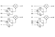
図8には、マルチバンドOFDMシステムで用いられるホッピングのための周波数合成ブロック(但し、グループAの3バンド・モードとする)の従来例を図解している(例えば、非特許文献1を参照のこと)。各バンドの中心周波数は、図示の通り、単一の発振器(例えば、TCXO)から得られる基準周波数を分周並びにミキサを用いて合成(周波数加減算)することができる。 FIG. 8 illustrates a conventional example of a frequency synthesis block for hopping used in a multiband OFDM system (however, a group A three-band mode) (see, for example, Non-Patent Document 1). about). As shown in the figure, the center frequency of each band can be synthesized (frequency addition / subtraction) using a mixer and a reference frequency obtained from a single oscillator (for example, TCXO).
同図に示す例では、発振器から出力される発振周波数をPLLにより逓倍して得られる周波数4224MHzを基準周波数とする。まず、8分の1分周により528MHzの周波数が取り出され、さらに2分の1分周により264MHzの周波数が取り出される。また、サンプル・クロックとして必要な528MHz分周により合成することができる。
In the example shown in the figure, the
次いで、SSB(Single Side Band)と記載されている各ミキサでは、528MHzと264MHzを用いて周波数的な加算を行ない、794MHzの周波数を得る。そして、選択器(Select)により264MHz又は794MHzの一方が選択され、後段のSSBにおいて所望の中心周波数を4224MHzと264MHzの周波数減算により3960MHzの周波数を得るとともに、4224MHzと264MHzの周波数加算により4488MHzの周波数を得、さらに4224MHzから792MHzの周波数減算により3422MHzの周波数を得ることができる。 Next, each mixer described as SSB (Single Side Band) performs frequency addition using 528 MHz and 264 MHz to obtain a frequency of 794 MHz. Then, one of 264 MHz and 794 MHz is selected by the selector (Select), the desired center frequency is obtained by subtracting the frequency of 4224 MHz and 264 MHz in the subsequent SSB, and the frequency of 4488 MHz is obtained by adding the frequencies of 4224 MHz and 264 MHz. Further, a frequency of 3422 MHz can be obtained by subtracting the frequency of 4224 MHz from 792 MHz.
図8中でSSBと記載されているミキサでは、それぞれの信号で互いに直交成分を用意し、下式に示すように三角関数の加法定理を用いて周波数の加算、減算を用いて周波数合成することができる。図9には周波数加算部の構成を示している。ここで、関数rot(x)をrot(x)=exp(2πjx)と定義する。 In the mixer described as SSB in FIG. 8, orthogonal components are prepared for each signal, and frequency synthesis is performed using frequency addition and subtraction using trigonometric addition theorem as shown in the following equation. Can do. FIG. 9 shows the configuration of the frequency adder. Here, the function rot (x) is defined as rot (x) = exp (2πjx).
また、図10には、グループAとグループCで構成される7バンド・モードに用いられる周波数合成ブロックの従来例を図解している。各バンドの中心周波数は、図示の通り、単一の発振器(例えば、TCXO)から得られる基準周波数を分周並びにミキサを用いて合成(周波数加減算)することができる。 FIG. 10 illustrates a conventional example of a frequency synthesis block used in the 7-band mode composed of group A and group C. As shown in the figure, the center frequency of each band can be synthesized (frequency addition / subtraction) using a mixer and a reference frequency obtained from a single oscillator (for example, TCXO).
同図に示す例では、発振器から出力される発振周波数をPLLにより逓倍して得られる周波数6336MHzを基準周波数とする。まず、3分の1分周により2112MHzの周波数が取り出され、続いて2分の1分周により1056MHzの周波数が取り出され、さらに2分の1分周が2回繰り返されて528MHz並びに264MHzの周波数が取り出される。また、サンプル・クロックとして必要な528MHzを分周により合成することができる。
In the example shown in the figure, the
また、同図に示す例では、周波数加減算を行なうSSBブロックが5個搭載されている。1つ目のSSBは、6336MHzと2112MHzの周波数減算により4224MHzの周波数を得る。また、2つ目のSSBは、1056MHzと528MHzの周波数加算により、1584MHzの周波数を得る。また、3つ目のSSBは、選択器により選択された1056MHz、1584MHz、528MHzのいずれかと6336MHzの周波数加減算を行なう。また、4つ目のSSBは、528MHzと264MHzの周波数加算により792MHzの周波数を得る。また、5つ目のSSBは、1つ目のSSBにより得られた4224MHzを、選択器により選択された792MHz又は264MHzのいずれかと周波数加減算する。そして、最終的には、3つ目のSSB又は4つ目のSSBとの周波数加減算結果が選択的に出力され、結果的に、グループA及びグループCで構成される7バンドの中心周波数を得ることができる。 In the example shown in the figure, five SSB blocks for frequency addition / subtraction are mounted. The first SSB obtains a frequency of 4224 MHz by subtracting the frequencies of 6336 MHz and 2112 MHz. The second SSB obtains a frequency of 1584 MHz by adding the frequencies of 1056 MHz and 528 MHz. The third SSB performs frequency addition / subtraction of 6336 MHz with any of 1056 MHz, 1584 MHz, and 528 MHz selected by the selector. The fourth SSB obtains a frequency of 792 MHz by adding the frequencies of 528 MHz and 264 MHz. The fifth SSB adds / subtracts the frequency of 4224 MHz obtained by the first SSB with either 792 MHz or 264 MHz selected by the selector. Finally, the frequency addition / subtraction result with the third SSB or the fourth SSB is selectively output, and as a result, the center frequency of 7 bands composed of group A and group C is obtained. be able to.
しかしながら、図8並びに図10に示したような従来の周波数合成ブロックにおいては、以下のような問題点がある。 However, the conventional frequency synthesis block as shown in FIGS. 8 and 10 has the following problems.
(1)SSBにおいては三角関数の加算定理を用いるため(図9を参照のこと)、528MHz、264MHzで直交成分(cosに対するsin成分)を求めなくてはならず、位相誤差を生じる原因となる。 (1) Since an addition theorem of a trigonometric function is used in SSB (see FIG. 9), an orthogonal component (sin component with respect to cos) must be obtained at 528 MHz and 264 MHz, which causes a phase error. .
(2)SSBにおいては三角関数の加法定理を用いているため、乗算、加算と複雑な演算を行なう必要があり、位相誤差、振幅誤差の原因となる。 (2) Since the addition theorem of trigonometric functions is used in SSB, it is necessary to perform complex operations such as multiplication and addition, which causes phase errors and amplitude errors.
(3)選択器(Select)はアナログ・スイッチで構成され、位相誤差や回路規模増大の原因となる。 (3) The selector (Select) is composed of an analog switch, and causes a phase error and an increase in circuit scale.
(4)特に図10に示した例ではSSBブロックの数が多く、乗算や加算など複雑な演算回路の規模が大きく、消費電力も大きくなる。 (4) Especially in the example shown in FIG. 10, the number of SSB blocks is large, the scale of complicated arithmetic circuits such as multiplication and addition is large, and the power consumption is also large.
例えば、UWB技術の適用例としての測距の解像度を向上するためには、マルチパス環境下における伝搬路特性を極力広帯域で細かい時間で測定し、受信信号の到来時刻τをより正確に測定することが重要である(これは、パルス幅が細かいことと同等である)。例えば1ナノ秒単位で測定することができると約30cmの分解能で測距を行なうことができる。 For example, in order to improve the resolution of ranging as an application example of the UWB technology, the propagation path characteristics in a multipath environment are measured in a minute time in a wide band as much as possible, and the arrival time τ of the received signal is measured more accurately. Is important (this is equivalent to a fine pulse width). For example, if measurement can be performed in units of 1 nanosecond, distance measurement can be performed with a resolution of about 30 cm.
他方、マルチバンドの無線通信システムにおいては、バンド毎に伝播路特性を推定することができる。ここで、各バンドにおける伝播路推定値をつなげて連続的な周波数特性と考えることにより、広帯域の伝搬路特性推定を実現することができる。しかしながら、サブバンド間で位相差があると、周波数特性は不連続となってしまうため、各サブバンドにおける伝搬路特性推定値を統合して広帯域の伝搬路特性推定値とすることはできない。 On the other hand, in a multiband wireless communication system, propagation path characteristics can be estimated for each band. Here, wideband propagation path characteristic estimation can be realized by connecting the propagation path estimated values in each band and considering it as a continuous frequency characteristic. However, if there is a phase difference between the subbands, the frequency characteristics become discontinuous. Therefore, it is impossible to integrate the propagation path characteristic estimation values in the respective subbands into a wideband propagation path characteristic estimation value.
本発明の目的は、複数のバンドからなるマルチバンド・システムにおける各バンドの中心周波数を好適に得ることができる、優れた周波数合成装置及び周波数合成方法を提供することにある。 An object of the present invention is to provide an excellent frequency synthesizer and a frequency synthesizer method capable of suitably obtaining the center frequency of each band in a multiband system composed of a plurality of bands.
本発明のさらなる目的は、基準となる周波数の分周と周波数加算により各バンドの中心周波数を好適に得ることができる、優れた周波数合成装置及び周波数合成方法を提供することにある。 A further object of the present invention is to provide an excellent frequency synthesizer and a frequency synthesizer method that can suitably obtain the center frequency of each band by frequency division and frequency addition as a reference.
本発明のさらなる目的は、位相誤差や振幅誤差なく各バンドの中心周波数を得ることができる、優れた周波数合成装置及び周波数合成方法を提供することにある。特に、各バンドの中心周波数の切替幅が大きいマルチバンド・システムに有効な優れた周波数合成装置及び周波数合成方法を提供する。 A further object of the present invention is to provide an excellent frequency synthesizer and frequency synthesizer method that can obtain the center frequency of each band without phase error and amplitude error. In particular, the present invention provides an excellent frequency synthesizer and a frequency synthesizer effective for a multiband system in which the switching frequency of the center frequency of each band is large.
本発明のさらなる目的は、比較的小さな回路規模並びに低い消費電力で各バンドの中心周波数を得ることができる、優れた周波数合成装置及び周波数合成方法を提供することにある。特に、本出願人に既に譲渡されている特願2003−294942において開示される、複数のサブバンドに渡る連続的な広帯域伝送路特性の推定に有効な、優れた周波数合成装置及び周波数合成方法を提供する。 A further object of the present invention is to provide an excellent frequency synthesizer and a frequency synthesizer method capable of obtaining the center frequency of each band with a relatively small circuit scale and low power consumption. In particular, an excellent frequency synthesizing apparatus and frequency synthesizing method that are effective for estimation of continuous broadband transmission line characteristics over a plurality of subbands disclosed in Japanese Patent Application No. 2003-294942 already assigned to the present applicant. provide.
本発明は、上記課題を参酌してなされたものであり、基準周波数を基に複数の周波数を合成する周波数合成装置であって、
複素平面上の8位相に対応する複素振幅を出力することにより、複素正弦波を生成する複素正弦波生成手段と、
前記複素正弦波と基準周波数を複素数乗算することにより周波数切り替えを行なう周波数切替手段と、
を具備することを特徴とする周波数合成装置である。
The present invention has been made in consideration of the above problems, and is a frequency synthesizer for synthesizing a plurality of frequencies based on a reference frequency,
A complex sine wave generating means for generating a complex sine wave by outputting a complex amplitude corresponding to eight phases on the complex plane;
Frequency switching means for performing frequency switching by multiplying the complex sine wave and a reference frequency by a complex number;
A frequency synthesizer characterized by comprising:
ここで、前記複素正弦波生成手段は、{−1.7,−0.7,0.7,1.7}の振幅を持つ2個の非線形DAコンバータで構成される。0.7はより具体的にはsqrt(0.5)すなわち0.5の平方根である。 Here, the complex sine wave generating means includes two nonlinear DA converters having amplitudes of {-1.7, -0.7, 0.7, 1.7}. More specifically, 0.7 is sqrt (0.5), that is, the square root of 0.5.
また、前記非線形DAコンバータの前記サンプリング周波数の1/2、1/4、1/8分周で出力される3ビットをデコードし、前記DAコンバータに対する入力データを決定する。このデコーダは、1/4、1/8分周を行なう際に、それぞれ90degの位相差を持つ分周出力を用いてデコードする。 In addition, 3 bits output at 1/2, 1/4, and 1/8 frequency division of the sampling frequency of the nonlinear DA converter are decoded to determine input data to the DA converter. This decoder performs decoding using divided outputs having a phase difference of 90 deg when performing 1/4 and 1/8 frequency division.
OFDM_UWBシステムにおけるグループAを構成する3バンドの中心周波数を生成する場合、本発明に係る周波数合成装置は、基準となる4224MHzの周波数を発振する発振器と、この基準周波数を1/2分周してサンプリング周波数としての2112MHzを得る分周器と、さらにこのサンプリング周波数を順次1/2分周する3個の分周器と、これら分周器からの1/2、1/4、1/8分周で出力される3ビットの値を周波数選択に応じてデコードするデコーダと、このデコーダによるデコード値を入力として{−1.7,−0.7,0.7,1.7}の振幅を出力する1組の非線形2ビットDAコンバータを用いて構成される。 When generating the center frequency of the three bands constituting the group A in the OFDM_UWB system, the frequency synthesizer according to the present invention oscillates a reference frequency of 4224 MHz, and divides this reference frequency by 1/2. A frequency divider that obtains 2112 MHz as a sampling frequency, three frequency dividers that sequentially divide this sampling frequency by 1/2, and 1/2, 1/4, and 1/8 minutes from these frequency dividers A decoder that decodes a 3-bit value output in a round according to frequency selection, and an amplitude of {-1.7, -0.7, 0.7, 1.7} with the decoded value by this decoder as an input It is configured using a set of non-linear 2-bit DA converters for output.
2組の非線形DAコンバータからは、複素平面上の8位相に対応する複素振幅が出力され、複素正弦波を生成することができる。したがって、位相の正方向に+1位相ずつ進むことにより、+264MHzが出力される。また、位相の正方向に−1位相ずつ進むことにより、−264MHzが出力される。また、位相の正方向に+3位相ずつ進むことにより、+792MHzが出力される。また、位相の正方向に−3位相ずつ進むことにより、−792MHzが出力される。 From the two sets of nonlinear DA converters, complex amplitudes corresponding to eight phases on the complex plane are output, and a complex sine wave can be generated. Therefore, +264 MHz is output by proceeding by +1 phase in the positive phase direction. Further, -264 MHz is output by proceeding by -1 phase in the positive phase direction. Further, +792 MHz is output by proceeding by +3 phases in the positive phase direction. In addition, by proceeding by -3 phases in the positive phase direction, -792 MHz is output.
そして、このような非線形DAコンバータの出力と、基準周波数である4224MHzと周波数加算(複素数乗算)を行なうことにより、マルチバンドOFDM_UWBシステムのグループAを構成する3バンドの各中心周波数4488MHz(=4224+264)、3960MHz(=4224−264)、3432MHz(=4224−792)を、位相誤差や振幅誤差なく得ることができる。
Then, by performing frequency addition (complex multiplication) with the output of such a nonlinear DA converter and the reference frequency of 4224 MHz, the center frequencies of 4 bands constituting group A of the
OFDM_UWBシステムにおけるグループAを構成する3バンドに加え、さらにグループCを構成する4バンドの中心周波数を生成する場合には、基準となる4224MHz以外に7128MHzの周波数を発振する発振器をさらに備える。また、前記周波数切替手段は、4224MHzと7128MHzいずれかの基準周波数と前記複素正弦波生成手段の各出力周波数を選択的に複素数乗算することにより、マルチバンドOFDM_UWBシステムのグループAを構成する3バンドの各中心周波数4488MHz、3960MHz、3432MHzを得るとともに、グループCを構成する各中心周波数7920MHz(=7128+792)、7392MHz(=7128+264)、6864MHz(=7128−264)、6336MHz(=7128−792)をさらに得ることができる。
In addition to the three bands constituting the group A in the OFDM_UWB system, when generating the center frequencies of the four bands constituting the group C, an oscillator for oscillating a frequency of 7128 MHz in addition to the
すなわち、本発明に係る周波数合成装置の構成によれば、マルチバンドOFDM_UWBシステムのグループAを構成する各中心周波数4488MHz、3960MHz、3432MHzのすべての周波数で全く同じ回路を用いるので、互いに位相差や振幅差などの誤差を生じない。また、回路的に大きな周波数加算の回路を1つしか用いないので、回路規模の削減や低消費電力化を実現することができる。
That is, according to the configuration of the frequency synthesizer according to the present invention, since the same circuit is used for all the
本発明によれば、広帯域の複数のバンドからなるマルチバンド・システムにおける各バンドの中心周波数を好適に得ることができる、優れた周波数合成装置及び周波数合成方法を提供することができる。 ADVANTAGE OF THE INVENTION According to this invention, the outstanding frequency synthesizer and frequency synthesizer method which can obtain suitably the center frequency of each band in the multiband system which consists of a several broadband band can be provided.
また、本発明によれば、基準となる周波数の分周と周波数加算により各バンドの中心周波数を好適に得ることができる、優れた周波数合成装置及び周波数合成方法を提供することができる。 Further, according to the present invention, it is possible to provide an excellent frequency synthesizer and frequency synthesizer method that can suitably obtain the center frequency of each band by frequency division and frequency addition as a reference.
また、本発明によれば、位相誤差や振幅誤差なく各バンドの中心周波数を得ることができる、優れた周波数合成装置及び周波数合成方法を提供することができる。 Further, according to the present invention, it is possible to provide an excellent frequency synthesizer and frequency synthesizer method that can obtain the center frequency of each band without phase error and amplitude error.
また、本発明によれば、比較的小さな回路規模並びに低い消費電力で各バンドの中心周波数を得ることができる、優れた周波数合成装置及び周波数合成方法を提供することができる。本発明に係る周波数合成装置は、回路規模の大きくなる周波数加算の回路を1つしか用いずにマルチバンドを合成することができるので、回路規模の削減と低消費電力化を実現することができる。 Further, according to the present invention, it is possible to provide an excellent frequency synthesizer and frequency synthesizer method that can obtain the center frequency of each band with a relatively small circuit scale and low power consumption. Since the frequency synthesizer according to the present invention can synthesize multibands without using only one frequency addition circuit that increases the circuit scale, the circuit scale can be reduced and the power consumption can be reduced. .
本発明のさらに他の目的、特徴や利点は、後述する本発明の実施形態や添付する図面に基づくより詳細な説明によって明らかになるであろう。 Other objects, features, and advantages of the present invention will become apparent from more detailed description based on embodiments of the present invention described later and the accompanying drawings.
以下、図面を参照しながら本発明の実施形態について詳解する。 Hereinafter, embodiments of the present invention will be described in detail with reference to the drawings.
図1には、本発明の一実施形態に係る周波数合成装置の構成を模式的に示している。図示の周波数合成装置は、例えばマルチバンドOFDM_UWB通信システムに適用され、基準となる周波数の分周と周波数加算により、グループAを構成する3バンドの各中心周波数を好適に得ることができる。 FIG. 1 schematically shows the configuration of a frequency synthesizer according to an embodiment of the present invention. The frequency synthesizer shown in the figure is applied to, for example, a multiband OFDM_UWB communication system, and can suitably obtain the center frequencies of the three bands constituting the group A by dividing the frequency as a reference and adding the frequencies.
図示の通り、周波数合成装置は、基準となる4224MHzの周波数を発振する発振器と、この基準周波数を1/2分周してサンプリング周波数としての2112MHzを得る分周器と、さらにこのサンプリング周波数を順次1/2分周する3個の分周器と、これら分周器からの1/2、1/4、1/8分周で出力される3ビットの値を周波数選択に応じてデコードするデコーダと、このデコーダによるデコード値を入力として{−1.7,−0.7,0.7,1.7}の振幅を出力する1組の非線形2ビットDAコンバータを備えている。ここで、0.7はより具体的にはsqrt(0.5)すなわち0.5の平方根である。この2組の非線形DAコンバータからは、複素平面上の8位相に対応する複素振幅が出力され、複素正弦波を生成することができる。そして、周波数変換部では、この複素正弦波を用いて周波数切り替えを行なう。 As shown in the figure, the frequency synthesizer includes an oscillator that oscillates a reference frequency of 4224 MHz, a frequency divider that divides this reference frequency by half to obtain 2112 MHz as a sampling frequency, and further, this sampling frequency. 3 frequency dividers that divide by 1/2, and a decoder that decodes 3-bit values output from the frequency dividers by 1/2, 1/4, and 1/8 frequency according to frequency selection And a set of non-linear 2-bit DA converters that output the amplitude of {-1.7, -0.7, 0.7, 1.7} using the decode value of this decoder as an input. Here, 0.7 is more specifically sqrt (0.5), that is, the square root of 0.5. From these two sets of nonlinear DA converters, complex amplitudes corresponding to eight phases on the complex plane are output, and a complex sine wave can be generated. In the frequency converter, the frequency is switched using this complex sine wave.
まず、基準となる422MHzがTCXO(温度補償型水晶発振器)などの発振器から出力され、これと同時に互いに90degの関係があるI軸、Q軸の各信号が取り出される。 First, 422 MHz serving as a reference is output from an oscillator such as a TCXO (temperature compensated crystal oscillator), and at the same time, each of the I-axis and Q-axis signals having a 90 deg relationship is extracted.
基準周波数のI軸信号は、さらに順次1/2分周を繰り返し、2112MHz、1056MHz、528MHz、264MHzの周波数が得られる。 The I-axis signal of the reference frequency is further sequentially divided by 1/2 to obtain frequencies of 2112 MHz, 1056 MHz, 528 MHz, and 264 MHz.
次いで、デコーダでは、非線形DAコンバータのサンプリング周波数の1/2,1/4,1/8分周すなわち1056MHz、528MHz、264MHzにおいて出力される3ビットからデコードを行なう。図2には、デコーダの真理値表を示している。 Next, the decoder performs decoding from 3 bits output at 1/2, 1/4, and 1/8 frequency division of the nonlinear DA converter, that is, 1056 MHz, 528 MHz, and 264 MHz. FIG. 2 shows a truth table of the decoder.
基準周波数のI軸信号を順次1/2分周を繰り返し、2112MHz、1056MHz、528MHz、264MHzの周波数を得る。図3には、分周出力のタイミング・チャートを示している。264MHz、528MHz、1056MHzを得るとき、同時に互いに90degの関係がある分周出力(AIに対するAQ、BIに対するBQ、CIに対するCQ)を得る。図2に示した真理値表の最左欄の3ビットは、AI、BI、CIの反転値からなる。 The I-axis signal of the reference frequency is sequentially divided by 1/2 to obtain frequencies of 2112 MHz, 1056 MHz, 528 MHz, and 264 MHz. FIG. 3 shows a timing chart of the divided output. When obtaining 264 MHz, 528 MHz, and 1056 MHz, frequency-divided outputs (AQ for AI, BQ for BI, and CQ for CI) are obtained at the same time. 3 bits in the leftmost column of the truth table shown in FIG. 2 are composed of inverted values of AI, BI, and CI.
ここで、AIに対するAQ、並びにBIに対するBQを用いて、図2に示した真理値表の簡単化を行ない、デコーダを図4に示すように簡単化することができる。但し、同図において、乗算器は排他的論理輪(XOR)回路で置き換えることができる。 Here, the truth table shown in FIG. 2 can be simplified using AQ for AI and BQ for BI, and the decoder can be simplified as shown in FIG. However, in the same figure, the multiplier can be replaced with an exclusive logical ring (XOR) circuit.
次いで、2個の非線形DAコンバータは、デコードされる数値を用いて、{00,01,10,11}の入力に対して、それぞれ{−1.7,−0.7,0.7,1.7}の振幅を得る。具体的には、デコードからの出力01は、DC成分オフセットにより±0.5にレベル変換される。そして、各非線形DAコンバータは、デコーダから出力されるI1及びI0、並びにQ1及びQ0をそれぞれ2.4倍及び1.0倍に増幅したものを合計して、I軸及びQ軸の1組の{−1.7,−0.7,0.7,1.7}の振幅を持つ複素振幅を2112MHzのタイミングで出力する。ここで、0.7はより具体的にはsqrt(0.5)すなわち0.5の平方根である。 The two nonlinear DA converters then use the decoded numbers to {-1.7, -0.7, 0.7, 1 for the input of {00, 01, 10, 11}, respectively. .7} amplitude. Specifically, the output 01 from the decode is level-converted to ± 0.5 by the DC component offset. Each nonlinear DA converter adds up I1 and I0 output from the decoder, and Q1 and Q0 amplified by 2.4 times and 1.0 times, respectively, and sets one set of I axis and Q axis. A complex amplitude having an amplitude of {-1.7, -0.7, 0.7, 1.7} is output at a timing of 2112 MHz. Here, 0.7 is more specifically sqrt (0.5), that is, the square root of 0.5.
図5には、2組の非線形DAコンバータの複素振幅を円周上にマッピングした様子を示している。同図に示すように、{−1.7,−0.7,0.7,1.7}の振幅を持つ各非線形DAコンバータからの出力は、円周上の8点にマッピングされる。 FIG. 5 shows a state where the complex amplitudes of the two sets of nonlinear DA converters are mapped on the circumference. As shown in the figure, outputs from the respective nonlinear DA converters having amplitudes of {-1.7, -0.7, 0.7, 1.7} are mapped to 8 points on the circumference.
2個の非線形DAコンバータの出力はI軸及びQ軸の1組として複素平面上の8点にマッピングされるが、これは、複素平面上の8位相に対応する複素振幅を出力することにより、複素正弦波を生成することを意味する。例えば、デコーダの出力が(11,10)であれば、非線形DAコンバータの出力は複素平面上の点((2.4×0.5+1×0.5),(2.4×0.5−0.5))=(1.7,0.7)にマッピングされる。また、デコーダの出力が(10,11)であれば、非線形DAコンバータの出力は複素平面上の点((2.4×0.5−0.5),(2.4×0.5+1×0.5))=(0.7,1.7)にマッピングされる。また、デコーダの出力が(01,11)であれば、非線形DAコンバータの出力は複素平面上の点((2.4×(−0.5)+0.5),(2.4×0.5+1×0.5))=(−0.7,1.7)にマッピングされる。また、デコーダの出力が(00,10)であれば、非線形DAコンバータの出力は複素平面上の点((2.4×(−0.5)−0.5),(2.4×0.5−0.5))=(−1.7,0.7)にマッピングされる。また、デコーダの出力が(00,01)であれば、非線形DAコンバータの出力は複素平面上の点((2.4×(−0.5)−0.5),(2.4×(−0.5)+1×0.5))=(−1.7,−0.7)にマッピングされる。また、デコーダの出力が(01,00)であれば、非線形DAコンバータの出力は複素平面上の点((2.4×(−0.5)+0.5,(2.4×(−0.5)+1×(−0.5))=(−0.7,−1.7)にマッピングされる。また、デコーダの出力が(10,00)であれば、非線形DAコンバータの出力は複素平面上の点((2.4×0.5−0.5,(2.4×(−0.5)+1×(−0.5))=(0.7,−1.7)にマッピングされる。また、デコーダの出力が(11,01)であれば、非線形DAコンバータの出力は複素平面上の点((2.4×0.5+1×0.5),(2.4×(−0.5)+0.5))=(1.7,−0.7)にマッピングされる。 The outputs of the two nonlinear DA converters are mapped to 8 points on the complex plane as a set of the I axis and the Q axis. By outputting complex amplitudes corresponding to 8 phases on the complex plane, It means to generate a complex sine wave. For example, if the output of the decoder is (11, 10), the output of the nonlinear DA converter is a point ((2.4 × 0.5 + 1 × 0.5), (2.4 × 0.5−) on the complex plane. 0.5)) = (1.7, 0.7). If the output of the decoder is (10, 11), the output of the nonlinear DA converter is a point ((2.4 × 0.5−0.5), (2.4 × 0.5 + 1 ×) on the complex plane. 0.5)) = (0.7, 1.7). If the output of the decoder is (01, 11), the output of the nonlinear DA converter is a point ((2.4 × (−0.5) +0.5), (2.4 × 0. 5 + 1 × 0.5)) = (− 0.7, 1.7). If the output of the decoder is (00, 10), the output of the nonlinear DA converter is a point ((2.4 × (−0.5) −0.5), (2.4 × 0) on the complex plane. .5-0.5)) = (-1.7, 0.7). If the output of the decoder is (00, 01), the output of the nonlinear DA converter is a point ((2.4 × (−0.5) −0.5), (2.4 × ( −0.5) + 1 × 0.5)) = (− 1.7, −0.7). If the output of the decoder is (01, 00), the output of the nonlinear DA converter is a point ((2.4 × (−0.5) +0.5, (2.4 × (−0) on the complex plane). .5) + 1 × (−0.5)) = (− 0.7, −1.7) If the output of the decoder is (10:00), the output of the nonlinear DA converter is Points on the complex plane ((2.4 × 0.5−0.5, (2.4 × (−0.5) + 1 × (−0.5)) = (0.7, −1.7) If the decoder output is (11, 01), the output of the nonlinear DA converter is a point ((2.4 × 0.5 + 1 × 0.5), (2.4) on the complex plane. × (−0.5) +0.5)) = (1.7, −0.7).
したがって、図5からも判るように、位相の正方向に+1位相ずつ進むことにより、+264MHzが出力される。また、位相の正方向に−1位相ずつ進むことにより、−264MHzが出力される。また、位相の正方向に+3位相ずつ進むことにより、+792MHzが出力される。また、位相の正方向に−3位相ずつ進むことにより、−792MHzが出力される。 Therefore, as can be seen from FIG. 5, +264 MHz is output by proceeding by +1 phase in the positive phase direction. Further, -264 MHz is output by proceeding by -1 phase in the positive phase direction. Further, +792 MHz is output by proceeding by +3 phases in the positive phase direction. In addition, by proceeding by -3 phases in the positive phase direction, -792 MHz is output.
周波数変換部(Frequency convert)では、このような非線形DAコンバータの出力と、基準周波数である4224MHzと周波数加算(複素数乗算)を行なうことにより、マルチバンドOFDM_UWBシステムのグループAを構成する3バンドの各中心周波数4488MHz(=4224+264)、3960MHz(=4224−264)、3432MHz(=4224−792)を、位相誤差や振幅誤差なく得ることができる。 The frequency conversion unit (Frequency convert) performs frequency addition (complex number multiplication) with the output of such a nonlinear DA converter and the reference frequency of 4224 MHz, so that each of the three bands constituting the group A of the multiband OFDM_UWB system A center frequency of 4488 MHz (= 4224 + 264), 3960 MHz (= 4224-264), and 3432 MHz (= 4224-792) can be obtained without phase error or amplitude error.
また、図6には、本発明の他の実施形態に係る周波数合成装置の構成を模式的に示している。図示の周波数合成装置は、例えばマルチバンドOFDM_UWB通信システムに適用され、基準となる周波数の分周と周波数加算により、グループA及びグループCを構成する合計4バンドの各中心周波数を好適に得ることができる。 FIG. 6 schematically shows a configuration of a frequency synthesizer according to another embodiment of the present invention. The frequency synthesizer shown in the figure is applied to, for example, a multiband OFDM_UWB communication system, and can suitably obtain the center frequencies of a total of four bands constituting group A and group C by dividing a frequency as a reference and adding the frequencies. it can.
図6に示す周波数合成装置は、図1に示したグループAの3バンドの中心周波数を生成する周波数合成装置に対し、さらにグループC用の4番どの中心周波数を生成する回路モジュールが追加されている。 The frequency synthesizer shown in FIG. 6 has a circuit module that generates the fourth center frequency for group C added to the frequency synthesizer that generates the center frequencies of the three bands of group A shown in FIG. Yes.
図示の例では、基準となる4224MHzの周波数を発振する発振器に加え、7128MHzの周波数を発振する発振器が装備されており、グループA又はグループCのいずれのモードに設定するかに応じて、選択的に切り替えて周波数変換部(Frequency convert)へ供給する。 In the example shown in the figure, an oscillator that oscillates a frequency of 7128 MHz is provided in addition to an oscillator that oscillates a frequency of 4224 MHz as a reference, and is selectively selected depending on whether the mode is set to group A or group C. To the frequency conversion unit (Frequency convert).
デコーダ及び非線形DAコンバータは、図1に示したものと略同一の構成である。すなわち、非線形DAコンバータは、複素平面上の8位相に対応する複素振幅を出力することにより、複素正弦波を生成する。 The decoder and the nonlinear DA converter have substantially the same configuration as that shown in FIG. That is, the nonlinear DA converter generates a complex sine wave by outputting a complex amplitude corresponding to 8 phases on the complex plane.
そして、周波数変換部(Frequency convert)では、このようなDAコンバータの出力と、基準周波数である4224MHzあるいは7128MHzとの周波数加算(複素数乗算)を選択的に行なうことにより、マルチバンドOFDM_UWBシステムのグループAを構成する3バンドの各中心周波数4488MHz(=4224+264)、3960MHz(=4224−264)、3432MHz(=4224−792)、あるいは同グループCを構成する4バンドの各中心周波数7920MHz(=7128+792)、7392MHz(=7128+264)、6864MHz(=7128−264)、6336MHz(=7128−792)を、位相誤差や振幅誤差なく選択的に得ることができる。
In the frequency converter, frequency output (complex number multiplication) between the output of the DA converter and the reference frequency of 4224 MHz or 7128 MHz is selectively performed, so that the group A of the multiband OFDM_UWB system is performed.
図1並びに図6に示したような周波数合成装置の構成によれば、マルチバンドOFDM_UWBシステムのグループAを構成する各中心周波数4488MHz、3960MHz、3432MHzのすべての周波数でまったく同じ回路を用いるので、互いに位相差や振幅差などの誤差を生じない。また、回路的に大きな周波数加算の回路を1つしか用いないので、回路規模の削減や低消費電力化を失言することができる。
According to the configuration of the frequency synthesizer as shown in FIG. 1 and FIG. 6, since the same circuit is used at all the
[追補]
以上、特定の実施形態を参照しながら、本発明について詳解してきた。しかしながら、本発明の要旨を逸脱しない範囲で当業者が該実施形態の修正や代用を成し得ることは自明である。すなわち、例示という形態で本発明を開示してきたのであり、本明細書の記載内容を限定的に解釈するべきではない。本発明の要旨を判断するためには、冒頭に記載した特許請求の範囲の欄を参酌すべきである。
[Supplement]
The present invention has been described in detail above with reference to specific embodiments. However, it is obvious that those skilled in the art can make modifications and substitutions of the embodiment without departing from the gist of the present invention. That is, the present invention has been disclosed in the form of exemplification, and the contents described in the present specification should not be interpreted in a limited manner. In order to determine the gist of the present invention, the claims section described at the beginning should be considered.
Claims (14)
複素平面上の8位相に対応する複素振幅を出力することにより、複素正弦波を生成する複素正弦波生成手段と、
前記複素正弦波と基準周波数を複素数乗算することにより周波数切り替えを行なう周波数切替手段と、
を具備することを特徴とする周波数合成装置。 A frequency synthesizer that synthesizes a plurality of frequencies based on a reference frequency,
A complex sine wave generating means for generating a complex sine wave by outputting a complex amplitude corresponding to eight phases on the complex plane;
Frequency switching means for performing frequency switching by multiplying the complex sine wave and a reference frequency by a complex number;
A frequency synthesizer characterized by comprising:
ことを特徴とする請求項1に記載の周波数合成装置。 The complex sine wave generating means is constituted by two nonlinear DA converters having amplitudes of {-1.7, -0.7, 0.7, 1.7}.
The frequency synthesizer according to claim 1.
前記サンプリング周波数の1/2、1/4、1/8分周で出力される3ビットをデコードして前記非線形DAコンバータに対する入力データを生成するデコーダと、
をさらに備えることを特徴とする請求項2に記載の周波数合成装置。 Frequency dividing means for sequentially dividing the sampling frequency of the nonlinear DA converter by 1/2,
A decoder that decodes 3 bits output at 1/2, 1/4, and 1/8 frequency of the sampling frequency to generate input data for the nonlinear DA converter;
The frequency synthesizer according to claim 2, further comprising:
ことを特徴とする請求項3に記載の周波数合成装置。 The decoder performs decoding using a divided output having a phase difference of 90 deg when performing 1/4 and 1/8 frequency division,
The frequency synthesizer according to claim 3.
前記複素正弦波生成手段は、前記複素平面上で位相の正方向に+1位相ずつ進むことにより+264MHzを出力し、位相の正方向に−1位相ずつ進むことにより−264MHzを出力し、位相の正方向に+3位相ずつ進むことにより+792MHzを出力し、位相の正方向に−3位相ずつ進むことにより−792MHzを出力し、
前記周波数切替手段は、該基準周波数と前記複素正弦波生成手段の各出力周波数を複素数乗算することにより、必要な周波数を得る、
ことを特徴とする請求項3に記載の周波数合成装置。 The reference frequency is 4224 MHz, 2112 MHz obtained by dividing the reference frequency by 1/2 is set as the sampling frequency of the nonlinear DA converter,
The complex sine wave generating means outputs +264 MHz by proceeding by +1 phase in the positive phase direction on the complex plane, and outputs -264 MHz by proceeding by −1 phase in the positive phase direction. +792 MHz is output by advancing by +3 phases in the direction, and -792 MHz is output by advancing by -3 phases in the positive direction of the phase,
The frequency switching unit obtains a necessary frequency by multiplying the reference frequency and each output frequency of the complex sine wave generation unit by a complex number.
The frequency synthesizer according to claim 3.
ことを特徴とする請求項3に記載の周波数合成装置。 The frequency switching unit obtains 4488 MHz, 3960 MHz, and 3432 MHz, which are center frequencies constituting the group A of the multiband OFDM_UWB system, by multiplying the reference frequency and each output frequency of the complex sine wave generation unit by a complex number.
The frequency synthesizer according to claim 3.
前記周波数切替手段は、4224MHz以外に7128MHzいずれかの基準周波数と前記複素正弦波生成手段の各出力周波数を選択的に複素数乗算することにより、マルチバンドOFDM_UWBシステムのグループCを構成する各中心周波数である7920MHz、7392MHz、6864MHz、6336MHzをさらに得る、
ことを特徴とする請求項6に記載の周波数合成装置。 In addition to the standard 4224 MHz, obtain a frequency of 7128 MHz,
The frequency switching means selectively multiplies each reference frequency of 7128 MHz in addition to 4224 MHz and each output frequency of the complex sine wave generation means by a complex number, so that each of the center frequencies constituting the group C of the multiband OFDM_UWB system. Further obtain certain 7920MHz, 7392MHz, 6864MHz, 6336MHz,
The frequency synthesizer according to claim 6.
複素平面上の8位相に対応する複素振幅を出力することにより、複素正弦波を生成する複素正弦波生成ステップと、
前記複素正弦波と基準周波数を複素数乗算することにより周波数切り替えを行なう周波数切替ステップと、
を具備することを特徴とする周波数合成方法。 A frequency synthesis method for synthesizing a plurality of frequencies based on a reference frequency,
A complex sine wave generating step for generating a complex sine wave by outputting a complex amplitude corresponding to eight phases on the complex plane;
A frequency switching step of performing frequency switching by multiplying the complex sine wave and a reference frequency by a complex number;
A frequency synthesizing method comprising:
ことを特徴とする請求項8に記載の周波数合成方法。 The complex sine wave generation step includes two sets of nonlinear DA conversion steps having amplitudes of {-1.7, -0.7, 0.7, 1.7}.
The frequency synthesizing method according to claim 8.
前記サンプリング周波数の1/2、1/4、1/8分周で出力される3ビットをデコードして前記DAコンバータに対する入力データを生成するデコーディング・ステップと、
をさらに備えることを特徴とする請求項9に記載の周波数合成方法。 A frequency dividing step of sequentially dividing the sampling frequency in the nonlinear DA conversion step by 1/2;
A decoding step of decoding 3 bits output at 1/2, 1/4, and 1/8 frequency of the sampling frequency to generate input data for the DA converter;
The frequency synthesis method according to claim 9, further comprising:
ことを特徴とする請求項10に記載の周波数合成方法。 In the decoding step, when performing 1/4 and 1/8 frequency division, decoding is performed using frequency division outputs each having a phase difference of 90 deg.
The frequency synthesizing method according to claim 10.
前記複素正弦波生成ステップでは、前記複素平面上で位相の正方向に+1位相ずつ進むことにより+264MHzを出力し、位相の正方向に−1位相ずつ進むことにより−264MHzを出力し、位相の正方向に+3位相ずつ進むことにより+792MHzを出力し、位相の正方向に−3位相ずつ進むことにより−792MHzを出力し、
前記周波数切替ステップでは、該基準周波数と前記複素正弦波生成ステップにおける各出力周波数を複素数乗算することにより、必要な周波数を得る、
ことを特徴とする請求項10に記載の周波数合成方法。 The reference frequency is 4224 MHz, and 2112 MHz obtained by dividing the reference frequency by 1/2 is set as the sampling frequency in the nonlinear DA conversion step.
In the complex sine wave generation step, +264 MHz is output by proceeding by +1 phase in the positive direction of the phase on the complex plane, and -264 MHz is output by proceeding by −1 phase in the positive direction of the phase. +792 MHz is output by advancing by +3 phases in the direction, and -792 MHz is output by advancing by -3 phases in the positive direction of the phase,
In the frequency switching step, a necessary frequency is obtained by multiplying each output frequency in the complex sine wave generation step by the complex number.
The frequency synthesizing method according to claim 10.
ことを特徴とする請求項10に記載の周波数合成方法。 In the frequency switching step, by multiplying the reference frequency and each output frequency in the complex sine wave generation step by a complex number, 4488 MHz, 3960 MHz, and 3432 MHz, which are center frequencies constituting the group A of the multiband OFDM_UWB system, are obtained.
The frequency synthesizing method according to claim 10.
前記周波数切替ステップでは、4224MHz以外に7128MHzいずれかの基準周波数と前記複素正弦波生成ステップにおける各出力周波数を選択的に複素数乗算することにより、マルチバンドOFDM_UWBシステムのグループCを構成する各中心周波数である7920MHz、7392MHz、6864MHz、6336MHzをさらに得る、
ことを特徴とする請求項13に記載の周波数合成方法。
In addition to the standard 4224 MHz, obtain a frequency of 7128 MHz,
In the frequency switching step, any reference frequency of 7128 MHz in addition to 4224 MHz and each output frequency in the complex sine wave generation step are selectively multiplied by complex numbers, so that each center frequency constituting group C of the multiband OFDM_UWB system is Further obtain certain 7920MHz, 7392MHz, 6864MHz, 6336MHz,
The frequency synthesis method according to claim 13.
Priority Applications (6)
| Application Number | Priority Date | Filing Date | Title |
|---|---|---|---|
| JP2003360249A JP2005129993A (en) | 2003-10-21 | 2003-10-21 | Frequency synthesizer and frequency synthesizer |
| KR20067007500A KR20060107514A (en) | 2003-10-21 | 2004-10-08 | Frequency synthesizer and frequency synthesis method |
| EP04792191A EP1677446A4 (en) | 2003-10-21 | 2004-10-08 | APPARATUS AND METHOD FOR FREQUENCY COMBINATION |
| PCT/JP2004/014922 WO2005039082A1 (en) | 2003-10-21 | 2004-10-08 | Frequency combining apparatus and frequency combining method |
| US10/575,082 US7593471B2 (en) | 2003-10-21 | 2004-10-08 | Frequency combining apparatus and frequency combining method |
| CN2004800285284A CN1860708B (en) | 2003-10-21 | 2004-10-08 | Frequency synthesis device and frequency synthesis method |
Applications Claiming Priority (1)
| Application Number | Priority Date | Filing Date | Title |
|---|---|---|---|
| JP2003360249A JP2005129993A (en) | 2003-10-21 | 2003-10-21 | Frequency synthesizer and frequency synthesizer |
Publications (1)
| Publication Number | Publication Date |
|---|---|
| JP2005129993A true JP2005129993A (en) | 2005-05-19 |
Family
ID=34463409
Family Applications (1)
| Application Number | Title | Priority Date | Filing Date |
|---|---|---|---|
| JP2003360249A Pending JP2005129993A (en) | 2003-10-21 | 2003-10-21 | Frequency synthesizer and frequency synthesizer |
Country Status (6)
| Country | Link |
|---|---|
| US (1) | US7593471B2 (en) |
| EP (1) | EP1677446A4 (en) |
| JP (1) | JP2005129993A (en) |
| KR (1) | KR20060107514A (en) |
| CN (1) | CN1860708B (en) |
| WO (1) | WO2005039082A1 (en) |
Cited By (5)
| Publication number | Priority date | Publication date | Assignee | Title |
|---|---|---|---|---|
| WO2005112292A1 (en) * | 2004-05-17 | 2005-11-24 | Nec Corporation | Signal generator, and transmitter, receiver, and transceiver using the same |
| JP2007258904A (en) * | 2006-03-22 | 2007-10-04 | Sony Corp | Wireless communication device |
| US7760791B2 (en) | 2006-01-10 | 2010-07-20 | Omron Corporation | Apparatus for communicating using UWB transmission |
| US7826814B2 (en) | 2006-06-09 | 2010-11-02 | Renesas Electronics Corporation | Frequency synthesizer |
| US8102895B2 (en) | 2007-07-02 | 2012-01-24 | Sony Corporation | Radio transmission apparatus, radio reception apparatus, transceiver, and radio communication method |
Families Citing this family (9)
| Publication number | Priority date | Publication date | Assignee | Title |
|---|---|---|---|---|
| KR100769678B1 (en) * | 2005-07-05 | 2007-10-24 | 삼성전자주식회사 | Frequency synthesizer |
| DE102005056952A1 (en) * | 2005-11-29 | 2007-06-14 | Infineon Technologies Ag | Circuit arrangement and method for generating local oscillator signals and phase locked loop with the circuit arrangement |
| US7809069B1 (en) * | 2006-01-13 | 2010-10-05 | Alereon, Inc. | Method and system for sidelobe reduction using antipodal signaling |
| CN101207598B (en) * | 2006-12-22 | 2010-12-15 | 财团法人工业技术研究院 | Frequency synthesizer and frequency synthesis method |
| CN102064846B (en) * | 2006-12-22 | 2012-10-03 | 财团法人工业技术研究院 | Frequency synthesizer and frequency synthesizing method |
| US8655934B2 (en) * | 2007-01-09 | 2014-02-18 | General Instrument Corporation | Broadband low noise complex regenerative frequency dividers |
| US7889751B2 (en) * | 2007-03-06 | 2011-02-15 | Sudhir Aggarwal | Low power wireless communication system |
| US8780834B2 (en) | 2009-04-15 | 2014-07-15 | Lg Electronics Inc. | Center frequency control method in wireless access system |
| US11656848B2 (en) * | 2019-09-18 | 2023-05-23 | Stmicroelectronics International N.V. | High throughput parallel architecture for recursive sinusoid synthesizer |
Family Cites Families (13)
| Publication number | Priority date | Publication date | Assignee | Title |
|---|---|---|---|---|
| JPS6384320A (en) | 1986-09-29 | 1988-04-14 | Matsushita Electric Ind Co Ltd | Microwave band frequency synthesizer |
| JPH0659031B2 (en) | 1987-08-31 | 1994-08-03 | 日本電気株式会社 | Phase locked oscillator |
| GB2215152B (en) | 1988-02-03 | 1992-03-18 | Secr Defence | Modulator circuit for synthesising a multiple sideband configuration |
| DE58908588D1 (en) * | 1988-10-18 | 1994-12-08 | Siemens Ag Albis | Frequency synthesizer. |
| JPH0612854B2 (en) | 1988-12-21 | 1994-02-16 | 日本電気株式会社 | Frequency synthesizer |
| JPH04288708A (en) | 1991-02-22 | 1992-10-13 | Mitsubishi Electric Corp | frequency synthesizer |
| JP3268138B2 (en) * | 1994-09-29 | 2002-03-25 | 三菱電機株式会社 | Communication device, frequency synthesizer and synthesis method |
| JPH1041816A (en) | 1996-07-24 | 1998-02-13 | Advantest Corp | Signal generator |
| JPH1155036A (en) * | 1997-08-04 | 1999-02-26 | Kokusai Electric Co Ltd | Frequency generation circuit |
| JPH11234047A (en) * | 1998-02-13 | 1999-08-27 | Kokusai Electric Co Ltd | Frequency conversion method and device |
| JP3797791B2 (en) | 1998-05-12 | 2006-07-19 | 新日本無線株式会社 | PLL synthesizer oscillator |
| GB0121713D0 (en) * | 2001-09-07 | 2001-10-31 | Nokia Corp | Accumulator based phase locked loop |
| JP4313542B2 (en) | 2002-03-29 | 2009-08-12 | 帝人株式会社 | Retardation film and method for producing the same |
-
2003
- 2003-10-21 JP JP2003360249A patent/JP2005129993A/en active Pending
-
2004
- 2004-10-08 KR KR20067007500A patent/KR20060107514A/en not_active Withdrawn
- 2004-10-08 WO PCT/JP2004/014922 patent/WO2005039082A1/en not_active Ceased
- 2004-10-08 CN CN2004800285284A patent/CN1860708B/en not_active Expired - Fee Related
- 2004-10-08 EP EP04792191A patent/EP1677446A4/en not_active Withdrawn
- 2004-10-08 US US10/575,082 patent/US7593471B2/en not_active Expired - Fee Related
Cited By (6)
| Publication number | Priority date | Publication date | Assignee | Title |
|---|---|---|---|---|
| WO2005112292A1 (en) * | 2004-05-17 | 2005-11-24 | Nec Corporation | Signal generator, and transmitter, receiver, and transceiver using the same |
| US7652542B2 (en) | 2004-05-17 | 2010-01-26 | Nec Corporation | Signal generator, and transmitter, receiver and transceiver using same |
| US7760791B2 (en) | 2006-01-10 | 2010-07-20 | Omron Corporation | Apparatus for communicating using UWB transmission |
| JP2007258904A (en) * | 2006-03-22 | 2007-10-04 | Sony Corp | Wireless communication device |
| US7826814B2 (en) | 2006-06-09 | 2010-11-02 | Renesas Electronics Corporation | Frequency synthesizer |
| US8102895B2 (en) | 2007-07-02 | 2012-01-24 | Sony Corporation | Radio transmission apparatus, radio reception apparatus, transceiver, and radio communication method |
Also Published As
| Publication number | Publication date |
|---|---|
| EP1677446A1 (en) | 2006-07-05 |
| KR20060107514A (en) | 2006-10-13 |
| EP1677446A4 (en) | 2011-12-21 |
| US7593471B2 (en) | 2009-09-22 |
| US20070071115A1 (en) | 2007-03-29 |
| CN1860708A (en) | 2006-11-08 |
| CN1860708B (en) | 2010-08-18 |
| WO2005039082A1 (en) | 2005-04-28 |
Similar Documents
| Publication | Publication Date | Title |
|---|---|---|
| KR101191835B1 (en) | Wireless communication device | |
| CN100596031C (en) | Sub-band UWB Communication System and Method | |
| US7593471B2 (en) | Frequency combining apparatus and frequency combining method | |
| JP4171466B2 (en) | Method and apparatus for generating a clock-based ultra-wideband transmission | |
| JP3918838B2 (en) | Image rejection mixer, multiband generator, and cascaded polyphase filter | |
| JP5450409B2 (en) | FFT / IFFT clock adjustment | |
| CN101860511B (en) | Wavenumber- division multiplexing transmission apparatus and methods thereof | |
| Esman et al. | Subnoise signal detection and communication | |
| JP2007295066A (en) | Ic for frequency hopping communication | |
| CN101432963A (en) | phase modulator | |
| JP6839679B2 (en) | Distance measurement system | |
| JP3838230B2 (en) | Propagation path characteristic estimation system, propagation path characteristic estimation method, communication apparatus, and communication method | |
| US7236513B2 (en) | Transmission method and transmitter | |
| JP3815423B2 (en) | Transmitting apparatus and transmitting method, receiving apparatus and receiving method, pulse position detecting method, and tracking method | |
| JP2008500788A (en) | Ultra Wideband OFDM Signal Transceiver Using Low Complexity CDMA Layer for Bandwidth Extension | |
| US6504879B1 (en) | Digital modulation apparatus | |
| JP5075630B2 (en) | Method for ultra-wideband communication using multiple codewords | |
| JP2004356927A (en) | Wireless communication device | |
| US8363690B2 (en) | Codeword synthesizing system and a correlation system, methods of operation thereof and a spread spectrum communications transceiver employing the same | |
| JP2006067520A (en) | Frequency synthesizer and frequency synthesizer | |
| JP2005123926A (en) | Transmitting apparatus and transmitting method | |
| JP2966810B2 (en) | Spread spectrum multiplexing communication equipment | |
| JP4211801B2 (en) | Transmission method and transmission apparatus | |
| CN107634786A (en) | A kind of frequency hopping communications emission system and method | |
| EP1745558B1 (en) | Pulse modulation and demodulation in a multiband UWB communication system |
Legal Events
| Date | Code | Title | Description |
|---|---|---|---|
| A621 | Written request for application examination |
Free format text: JAPANESE INTERMEDIATE CODE: A621 Effective date: 20061003 |
|
| A131 | Notification of reasons for refusal |
Free format text: JAPANESE INTERMEDIATE CODE: A131 Effective date: 20090526 |
|
| A02 | Decision of refusal |
Free format text: JAPANESE INTERMEDIATE CODE: A02 Effective date: 20091006 |