JP2005104770A - Dielectric ceramic composition and electronic component - Google Patents
Dielectric ceramic composition and electronic component Download PDFInfo
- Publication number
- JP2005104770A JP2005104770A JP2003340577A JP2003340577A JP2005104770A JP 2005104770 A JP2005104770 A JP 2005104770A JP 2003340577 A JP2003340577 A JP 2003340577A JP 2003340577 A JP2003340577 A JP 2003340577A JP 2005104770 A JP2005104770 A JP 2005104770A
- Authority
- JP
- Japan
- Prior art keywords
- dielectric
- oxide
- multilayer ceramic
- mol
- ceramic capacitor
- Prior art date
- Legal status (The legal status is an assumption and is not a legal conclusion. Google has not performed a legal analysis and makes no representation as to the accuracy of the status listed.)
- Pending
Links
- 239000000203 mixture Substances 0.000 title claims abstract description 60
- 239000000919 ceramic Substances 0.000 title claims abstract description 40
- 239000003985 ceramic capacitor Substances 0.000 claims abstract description 48
- 239000003990 capacitor Substances 0.000 claims abstract description 25
- 239000002245 particle Substances 0.000 claims description 15
- 229910000990 Ni alloy Inorganic materials 0.000 claims description 11
- 239000004020 conductor Substances 0.000 claims description 11
- 239000013078 crystal Substances 0.000 claims description 11
- 239000003989 dielectric material Substances 0.000 claims description 7
- 229910004298 SiO 2 Inorganic materials 0.000 claims description 4
- 229910052814 silicon oxide Inorganic materials 0.000 abstract description 4
- 239000010410 layer Substances 0.000 description 85
- 230000007547 defect Effects 0.000 description 31
- 238000010304 firing Methods 0.000 description 31
- 238000000034 method Methods 0.000 description 16
- 239000011230 binding agent Substances 0.000 description 15
- 239000007789 gas Substances 0.000 description 14
- 230000007423 decrease Effects 0.000 description 12
- 230000000694 effects Effects 0.000 description 12
- 238000000137 annealing Methods 0.000 description 11
- QVGXLLKOCUKJST-UHFFFAOYSA-N atomic oxygen Chemical compound [O] QVGXLLKOCUKJST-UHFFFAOYSA-N 0.000 description 11
- 229910052760 oxygen Inorganic materials 0.000 description 11
- 239000001301 oxygen Substances 0.000 description 11
- 238000009413 insulation Methods 0.000 description 10
- 229910052759 nickel Inorganic materials 0.000 description 9
- 230000000052 comparative effect Effects 0.000 description 7
- XLYOFNOQVPJJNP-UHFFFAOYSA-N water Substances O XLYOFNOQVPJJNP-UHFFFAOYSA-N 0.000 description 7
- 230000002159 abnormal effect Effects 0.000 description 6
- 239000002003 electrode paste Substances 0.000 description 6
- 150000001875 compounds Chemical class 0.000 description 5
- 239000000843 powder Substances 0.000 description 5
- CSCPPACGZOOCGX-UHFFFAOYSA-N Acetone Chemical compound CC(C)=O CSCPPACGZOOCGX-UHFFFAOYSA-N 0.000 description 4
- 229920002799 BoPET Polymers 0.000 description 4
- 229910045601 alloy Inorganic materials 0.000 description 4
- 239000000956 alloy Substances 0.000 description 4
- 239000010953 base metal Substances 0.000 description 4
- 238000001816 cooling Methods 0.000 description 4
- 230000002950 deficient Effects 0.000 description 4
- 238000011156 evaluation Methods 0.000 description 4
- 239000003973 paint Substances 0.000 description 4
- 230000000630 rising effect Effects 0.000 description 4
- 238000005245 sintering Methods 0.000 description 4
- YMWUJEATGCHHMB-UHFFFAOYSA-N Dichloromethane Chemical compound ClCCl YMWUJEATGCHHMB-UHFFFAOYSA-N 0.000 description 3
- YXFVVABEGXRONW-UHFFFAOYSA-N Toluene Chemical compound CC1=CC=CC=C1 YXFVVABEGXRONW-UHFFFAOYSA-N 0.000 description 3
- 239000000463 material Substances 0.000 description 3
- 239000003960 organic solvent Substances 0.000 description 3
- 238000005498 polishing Methods 0.000 description 3
- 238000012545 processing Methods 0.000 description 3
- 239000000758 substrate Substances 0.000 description 3
- 238000011282 treatment Methods 0.000 description 3
- 239000004925 Acrylic resin Substances 0.000 description 2
- 229920000178 Acrylic resin Polymers 0.000 description 2
- IRIAEXORFWYRCZ-UHFFFAOYSA-N Butylbenzyl phthalate Chemical compound CCCCOC(=O)C1=CC=CC=C1C(=O)OCC1=CC=CC=C1 IRIAEXORFWYRCZ-UHFFFAOYSA-N 0.000 description 2
- 239000001856 Ethyl cellulose Substances 0.000 description 2
- ZZSNKZQZMQGXPY-UHFFFAOYSA-N Ethyl cellulose Chemical compound CCOCC1OC(OC)C(OCC)C(OCC)C1OC1C(O)C(O)C(OC)C(CO)O1 ZZSNKZQZMQGXPY-UHFFFAOYSA-N 0.000 description 2
- 239000000654 additive Substances 0.000 description 2
- WUOACPNHFRMFPN-UHFFFAOYSA-N alpha-terpineol Chemical compound CC1=CCC(C(C)(C)O)CC1 WUOACPNHFRMFPN-UHFFFAOYSA-N 0.000 description 2
- 239000002131 composite material Substances 0.000 description 2
- 239000000470 constituent Substances 0.000 description 2
- SQIFACVGCPWBQZ-UHFFFAOYSA-N delta-terpineol Natural products CC(C)(O)C1CCC(=C)CC1 SQIFACVGCPWBQZ-UHFFFAOYSA-N 0.000 description 2
- 239000002270 dispersing agent Substances 0.000 description 2
- 229920001249 ethyl cellulose Polymers 0.000 description 2
- 235000019325 ethyl cellulose Nutrition 0.000 description 2
- 238000004898 kneading Methods 0.000 description 2
- 238000005259 measurement Methods 0.000 description 2
- 229910052751 metal Inorganic materials 0.000 description 2
- 239000002184 metal Substances 0.000 description 2
- 150000002902 organometallic compounds Chemical class 0.000 description 2
- 230000001681 protective effect Effects 0.000 description 2
- 238000005488 sandblasting Methods 0.000 description 2
- 239000002002 slurry Substances 0.000 description 2
- 229940116411 terpineol Drugs 0.000 description 2
- 239000003232 water-soluble binding agent Substances 0.000 description 2
- UOCLXMDMGBRAIB-UHFFFAOYSA-N 1,1,1-trichloroethane Chemical compound CC(Cl)(Cl)Cl UOCLXMDMGBRAIB-UHFFFAOYSA-N 0.000 description 1
- OAYXUHPQHDHDDZ-UHFFFAOYSA-N 2-(2-butoxyethoxy)ethanol Chemical compound CCCCOCCOCCO OAYXUHPQHDHDDZ-UHFFFAOYSA-N 0.000 description 1
- 229910052692 Dysprosium Inorganic materials 0.000 description 1
- 229910052688 Gadolinium Inorganic materials 0.000 description 1
- 229910002651 NO3 Inorganic materials 0.000 description 1
- NHNBFGGVMKEFGY-UHFFFAOYSA-N Nitrate Chemical compound [O-][N+]([O-])=O NHNBFGGVMKEFGY-UHFFFAOYSA-N 0.000 description 1
- 229910001252 Pd alloy Inorganic materials 0.000 description 1
- 239000004372 Polyvinyl alcohol Substances 0.000 description 1
- 229910052771 Terbium Inorganic materials 0.000 description 1
- 239000002253 acid Chemical class 0.000 description 1
- 230000000996 additive effect Effects 0.000 description 1
- 229910052782 aluminium Inorganic materials 0.000 description 1
- QRUDEWIWKLJBPS-UHFFFAOYSA-N benzotriazole Chemical compound C1=CC=C2N[N][N]C2=C1 QRUDEWIWKLJBPS-UHFFFAOYSA-N 0.000 description 1
- 239000012964 benzotriazole Substances 0.000 description 1
- 230000015572 biosynthetic process Effects 0.000 description 1
- 229910052793 cadmium Inorganic materials 0.000 description 1
- 150000004649 carbonic acid derivatives Chemical class 0.000 description 1
- 239000001913 cellulose Substances 0.000 description 1
- 229920002678 cellulose Polymers 0.000 description 1
- 229910052804 chromium Inorganic materials 0.000 description 1
- 239000011248 coating agent Substances 0.000 description 1
- 239000011247 coating layer Substances 0.000 description 1
- 238000000576 coating method Methods 0.000 description 1
- 229910052802 copper Inorganic materials 0.000 description 1
- 238000000280 densification Methods 0.000 description 1
- 238000009792 diffusion process Methods 0.000 description 1
- 230000002349 favourable effect Effects 0.000 description 1
- XLYOFNOQVPJJNP-UHFFFAOYSA-M hydroxide Chemical compound [OH-] XLYOFNOQVPJJNP-UHFFFAOYSA-M 0.000 description 1
- 229910052500 inorganic mineral Inorganic materials 0.000 description 1
- 239000012212 insulator Substances 0.000 description 1
- 239000011229 interlayer Substances 0.000 description 1
- 238000010030 laminating Methods 0.000 description 1
- 229910052748 manganese Inorganic materials 0.000 description 1
- 238000004519 manufacturing process Methods 0.000 description 1
- 150000002739 metals Chemical class 0.000 description 1
- 239000011707 mineral Substances 0.000 description 1
- 229910052750 molybdenum Inorganic materials 0.000 description 1
- 230000007935 neutral effect Effects 0.000 description 1
- 230000003647 oxidation Effects 0.000 description 1
- 238000007254 oxidation reaction Methods 0.000 description 1
- 229910052763 palladium Inorganic materials 0.000 description 1
- 229910052698 phosphorus Inorganic materials 0.000 description 1
- 239000004014 plasticizer Substances 0.000 description 1
- 238000007747 plating Methods 0.000 description 1
- 229920002037 poly(vinyl butyral) polymer Polymers 0.000 description 1
- 229920000139 polyethylene terephthalate Polymers 0.000 description 1
- 229920002451 polyvinyl alcohol Polymers 0.000 description 1
- 229910052573 porcelain Inorganic materials 0.000 description 1
- 230000001737 promoting effect Effects 0.000 description 1
- 150000003839 salts Chemical class 0.000 description 1
- 238000005476 soldering Methods 0.000 description 1
- 235000015096 spirit Nutrition 0.000 description 1
- 239000000126 substance Substances 0.000 description 1
- 238000003786 synthesis reaction Methods 0.000 description 1
- 229910052716 thallium Inorganic materials 0.000 description 1
- 229910052718 tin Inorganic materials 0.000 description 1
- 229910052720 vanadium Inorganic materials 0.000 description 1
- 229910052727 yttrium Inorganic materials 0.000 description 1
- 229910052725 zinc Inorganic materials 0.000 description 1
- 229910052726 zirconium Inorganic materials 0.000 description 1
Images


Classifications
-
- H—ELECTRICITY
- H01—ELECTRIC ELEMENTS
- H01G—CAPACITORS; CAPACITORS, RECTIFIERS, DETECTORS, SWITCHING DEVICES, LIGHT-SENSITIVE OR TEMPERATURE-SENSITIVE DEVICES OF THE ELECTROLYTIC TYPE
- H01G4/00—Fixed capacitors; Processes of their manufacture
- H01G4/002—Details
- H01G4/018—Dielectrics
- H01G4/06—Solid dielectrics
- H01G4/08—Inorganic dielectrics
- H01G4/12—Ceramic dielectrics
- H01G4/1209—Ceramic dielectrics characterised by the ceramic dielectric material
- H01G4/1218—Ceramic dielectrics characterised by the ceramic dielectric material based on titanium oxides or titanates
- H01G4/1227—Ceramic dielectrics characterised by the ceramic dielectric material based on titanium oxides or titanates based on alkaline earth titanates
-
- C—CHEMISTRY; METALLURGY
- C04—CEMENTS; CONCRETE; ARTIFICIAL STONE; CERAMICS; REFRACTORIES
- C04B—LIME, MAGNESIA; SLAG; CEMENTS; COMPOSITIONS THEREOF, e.g. MORTARS, CONCRETE OR LIKE BUILDING MATERIALS; ARTIFICIAL STONE; CERAMICS; REFRACTORIES; TREATMENT OF NATURAL STONE
- C04B35/00—Shaped ceramic products characterised by their composition; Ceramics compositions; Processing powders of inorganic compounds preparatory to the manufacturing of ceramic products
- C04B35/01—Shaped ceramic products characterised by their composition; Ceramics compositions; Processing powders of inorganic compounds preparatory to the manufacturing of ceramic products based on oxide ceramics
- C04B35/46—Shaped ceramic products characterised by their composition; Ceramics compositions; Processing powders of inorganic compounds preparatory to the manufacturing of ceramic products based on oxide ceramics based on titanium oxides or titanates
- C04B35/462—Shaped ceramic products characterised by their composition; Ceramics compositions; Processing powders of inorganic compounds preparatory to the manufacturing of ceramic products based on oxide ceramics based on titanium oxides or titanates based on titanates
- C04B35/465—Shaped ceramic products characterised by their composition; Ceramics compositions; Processing powders of inorganic compounds preparatory to the manufacturing of ceramic products based on oxide ceramics based on titanium oxides or titanates based on titanates based on alkaline earth metal titanates
- C04B35/468—Shaped ceramic products characterised by their composition; Ceramics compositions; Processing powders of inorganic compounds preparatory to the manufacturing of ceramic products based on oxide ceramics based on titanium oxides or titanates based on titanates based on alkaline earth metal titanates based on barium titanates
-
- H—ELECTRICITY
- H01—ELECTRIC ELEMENTS
- H01G—CAPACITORS; CAPACITORS, RECTIFIERS, DETECTORS, SWITCHING DEVICES, LIGHT-SENSITIVE OR TEMPERATURE-SENSITIVE DEVICES OF THE ELECTROLYTIC TYPE
- H01G4/00—Fixed capacitors; Processes of their manufacture
- H01G4/30—Stacked capacitors
Landscapes
- Engineering & Computer Science (AREA)
- Power Engineering (AREA)
- Chemical & Material Sciences (AREA)
- Ceramic Engineering (AREA)
- Manufacturing & Machinery (AREA)
- Microelectronics & Electronic Packaging (AREA)
- Inorganic Chemistry (AREA)
- Structural Engineering (AREA)
- Organic Chemistry (AREA)
- Materials Engineering (AREA)
- Ceramic Capacitors (AREA)
- Compositions Of Oxide Ceramics (AREA)
- Inorganic Insulating Materials (AREA)
- Fixed Capacitors And Capacitor Manufacturing Machines (AREA)
- Laminated Bodies (AREA)
Abstract
Description
本発明は、たとえば積層セラミックコンデンサの誘電体層などとして用いられる誘電体磁器組成物と、その誘電体磁器組成物を誘電体層として用いる電子部品に関する。 The present invention relates to a dielectric ceramic composition used as, for example, a dielectric layer of a multilayer ceramic capacitor, and an electronic component using the dielectric ceramic composition as a dielectric layer.
積層型セラミックコンデンサは、小型、大容量、高信頼性の電子部品として広く利用されており、電気機器および電子機器の中で使用される個数も多数にのぼる。近年、機器の小型且つ高性能化に伴い、積層セラミックコンデンサに対する更なる小型化、大容量化、低価格化、高信頼性化への要求はますます厳しくなっている。 Multilayer ceramic capacitors are widely used as small-sized, large-capacity, and high-reliability electronic components, and the number used in electrical and electronic devices is large. In recent years, with the miniaturization and high performance of devices, the demand for further miniaturization, large capacity, low price, and high reliability of multilayer ceramic capacitors has become increasingly severe.
積層型セラミックコンデンサは、通常、内部電極のペーストと誘電体のスラリー(ペースト)とを、シート法や印刷法等により積層し、焼成して製造される。かかる内部電極には、一般に、PdやPd合金が用いられてきたが、Pdは高価であるため、比較的安価なNiやNi合金が使用されつつある。 A multilayer ceramic capacitor is usually manufactured by laminating an internal electrode paste and a dielectric slurry (paste) by a sheet method, a printing method, or the like, followed by firing. In general, Pd and Pd alloys have been used for such internal electrodes. However, since Pd is expensive, relatively inexpensive Ni and Ni alloys are being used.
ところで、内部電極をNiやNi合金で形成する場合は、大気中で焼成を行うと電極が酸化してしまうという問題がある。このため、一般に、脱バインダ後は、中性または還元性雰囲気下で焼成する必要がある。 By the way, when the internal electrode is formed of Ni or Ni alloy, there is a problem that the electrode is oxidized if firing is performed in the atmosphere. For this reason, generally, after removing the binder, it is necessary to fire in a neutral or reducing atmosphere.
しかし、NiやNi合金製の内部電極を有する積層セラミックコンデンサは、大気中で焼成して製造されるPd製の内部電極を有する積層セラミックコンデンサに比べ、絶縁抵抗の寿命性能が短く、信頼性が低いという問題があった。 However, a multilayer ceramic capacitor having an internal electrode made of Ni or Ni alloy has a shorter insulation resistance life performance and reliability than a multilayer ceramic capacitor having a Pd internal electrode manufactured by firing in the atmosphere. There was a problem of being low.
NiやNi合金製の内部電極を有する積層セラミックコンデンサにおいて、絶縁抵抗の寿命性能を向上させることができる誘電体磁器組成物として、特許文献1、特許文献2で開示されているようなものが知られている。
In a multilayer ceramic capacitor having an internal electrode made of Ni or Ni alloy, as a dielectric ceramic composition capable of improving the life performance of insulation resistance, those disclosed in
特許文献1によると、ある特定の組成を有する誘電体酸化物を含有し、Y、Gd、Tb、Dy、Zr、V、Mo、Zn、Cd、Tl、SnおよびPの酸化物および/または焼成により酸化物になる化合物から選ばれる一種以上を、特定量添加した誘電体誘電体磁器組成物を使用することにより、絶縁抵抗の寿命性能を向上させることができる。
According to
また、特許文献2によると、ある特定の組成を有する誘電体酸化物を含有し、Mnの酸化物および/または焼成により酸化物になる化合物と、Yの酸化物および/または焼成により酸化物になる化合物とを、特定量添加した誘電体誘電体磁器組成物を使用することにより、さらなる絶縁抵抗の寿命性能を向上させることができる。
Further, according to
また、上記特許文献1または特許文献2に開示されている誘電体磁器組成物においては、主成分である{{Ba(1−x−y)CaxSry}O}A{Ti(1−z)Zrz}BO2に、副成分としてMg酸化物を添加できる旨が記載されている。しかしながら、これらの文献では、積層セラミックコンデンサを薄層化(たとえば4.5μm以下)した場合に、初期絶縁抵抗不良率つまり、IR不良率を低くするためのMg量とCa量との組成範囲に関しては何ら開示されていない。また、特許文献1記載の誘電体磁器組成物は、Caの含有量が多いため比誘電率が低くなってしまうという問題も抱えている。
In the dielectric ceramic composition disclosed in
本発明の目的は、積層セラミックコンデンサの誘電体層として使用し、積層セラミックコンデンサを薄層化した場合においても、IR不良率を低く抑えることができ、かつ高い比誘電率を有する誘電体磁器組成物を提供することである。また、本発明は、このような誘電体磁器組成物を用いて製造され、信頼性が高められた積層セラミックコンデンサなどの電子部品を提供することも目的とする。特に本発明は、薄層化、小型化対応の積層セラミックコンデンサ等の電子部品を提供することを目的としている。 An object of the present invention is to use a dielectric ceramic composition that can be used as a dielectric layer of a multilayer ceramic capacitor, and that the IR defect rate can be kept low even when the multilayer ceramic capacitor is thinned, and that has a high relative dielectric constant. Is to provide things. Another object of the present invention is to provide an electronic component such as a multilayer ceramic capacitor manufactured using such a dielectric ceramic composition and having improved reliability. In particular, an object of the present invention is to provide an electronic component such as a multilayer ceramic capacitor capable of being thinned and miniaturized.
本発明の発明者等は、積層セラミックコンデンサなどの電子部品の誘電体層として用いられる誘電体磁器組成物において、積層セラミックコンデンサの誘電体層として使用し、積層セラミックコンデンサを薄層化しても、IR不良率を低く抑えることができ、かつ高い比誘電率を有する誘電体磁器組成物について鋭意検討した結果、主成分と副成分からなる誘電体磁器組成物において、Mg原子を含有し、組成式{{Ba(1−x)Cax}O}A{Ti(1−y−z)ZryMgz}BO2で表される誘電体材料を主成分とし、該主成分の組成比を限定することで、本発明の目的を達成できることを見出し、本発明を完成させるに至った。 The inventors of the present invention use a dielectric ceramic composition used as a dielectric layer of an electronic component such as a multilayer ceramic capacitor as a dielectric layer of the multilayer ceramic capacitor, and even if the multilayer ceramic capacitor is thinned, As a result of intensive studies on a dielectric ceramic composition having a low IR defect rate and a high relative dielectric constant, a dielectric ceramic composition comprising a main component and a subcomponent contains Mg atoms, and a composition formula {{Ba (1-x) Ca x } O} A {Ti (1-yz) Zr y Mg z } B O 2 as a main component, and the composition ratio of the main component is By limiting, it discovered that the objective of this invention could be achieved and came to complete this invention.
すなわち、本発明に係る誘電体磁器組成物は、
組成式{{Ba(1−x)Cax}O}A{Ti(1−y−z)ZryMgz}BO2
(ただし、A,B,x,y,zが、0.995≦A/B≦1.020、0.0001≦x≦0.07、0.1≦y≦0.3、0.0005≦z≦0.01)
で表される主成分と、
副成分として、主成分100モルに対して、Mnの酸化物をMnO換算で0.03〜1.7モルと、Yの酸化物をY2O3換算で0.05〜0.5モルと、Vの酸化物をV2O5換算で0.007〜0.4モルと、Siの酸化物をSiO2換算で0〜0.5モルとを含有することを特徴とする。
That is, the dielectric ceramic composition according to the present invention is
Compositional Formula {{Ba (1-x) Ca x } O} A {Ti (1-y-z) Zr y Mg z } B O 2
(However, A, B, x, y, z are 0.995 ≦ A / B ≦ 1.020, 0.0001 ≦ x ≦ 0.07, 0.1 ≦ y ≦ 0.3, 0.0005 ≦ z ≦ 0.01)
A main component represented by
As subcomponents, the oxide of Mn is 0.03 to 1.7 mol in terms of MnO and the oxide of Y is 0.05 to 0.5 mol in terms of Y 2 O 3 with respect to 100 mol of the main component. The oxide of V contains 0.007 to 0.4 mol in terms of V 2 O 5 and the oxide of Si contains 0 to 0.5 mol in terms of SiO 2 .
本発明に係る誘電体磁器組成物は、好ましくは副成分として、さらに、Wの酸化物を、主成分100モルに対して、WO3換算で0.005〜0.3モル含有する。 The dielectric ceramic composition according to the present invention preferably further contains, as a subcomponent, 0.005 to 0.3 mol of an oxide of W in terms of WO 3 with respect to 100 mol of the main component.
本発明に係る電子部品は、上記のいずれかに記載の誘電体磁器組成物で構成してある誘電体層を有する。電子部品としては、特に限定されないが、積層セラミックコンデンサ、圧電素子、チップインダクタ、チップバリスタ、チップサーミスタ、チップ抵抗、その他の表面実装(SMD)チップ型電子部品が例示される。 The electronic component according to the present invention has a dielectric layer made of any one of the above dielectric ceramic compositions. Although it does not specifically limit as an electronic component, A multilayer ceramic capacitor, a piezoelectric element, a chip inductor, a chip varistor, a chip thermistor, a chip resistor, and other surface mount (SMD) chip type electronic components are illustrated.
本発明に係る積層セラミックコンデンサは、上記のいずれかに記載の誘電体磁器組成物で構成してある誘電体層と、内部電極層とが交互に積層してあるコンデンサ素子本体を有する。 A multilayer ceramic capacitor according to the present invention has a capacitor element body in which dielectric layers composed of the dielectric ceramic composition described above and internal electrode layers are alternately stacked.
本発明に係る積層セラミックコンデンサにおいて、好ましくは、前記内部電極層に含まれる導電材がNiまたはNi合金である。 In the multilayer ceramic capacitor according to the present invention, preferably, the conductive material included in the internal electrode layer is Ni or a Ni alloy.
本発明に係る積層セラミックコンデンサにおいて、好ましくは、前記誘電体層の積層数が、50以上である。 In the multilayer ceramic capacitor according to the present invention, preferably, the number of the dielectric layers is 50 or more.
本発明に係る積層セラミックコンデンサにおいて、好ましくは、前記誘電体層の厚みが、4.5μm以下である。 In the multilayer ceramic capacitor according to the present invention, preferably, the dielectric layer has a thickness of 4.5 μm or less.
本発明に係る積層セラミックコンデンサにおいて、好ましくは、前記誘電体層を構成する誘電体粒子の平均結晶粒径(R)と、前記誘電体層の厚み(d)との比(R/d)が、0.5<R/d<3である。 In the multilayer ceramic capacitor according to the present invention, preferably, a ratio (R / d) between an average crystal grain size (R) of dielectric particles constituting the dielectric layer and a thickness (d) of the dielectric layer is set. 0.5 <R / d <3.
本発明に係る積層セラミックコンデンサにおいて、好ましくは、前記内部電極層が前記誘電体層を被覆する面積の被覆率が、60〜100%である。 In the multilayer ceramic capacitor according to the present invention, preferably, a coverage of an area where the internal electrode layer covers the dielectric layer is 60 to 100%.
本発明によれば、積層セラミックコンデンサの誘電体層を薄層化、多層化した場合においても、IR不良率を低く抑えることができ、高い比誘電率を有する誘電体磁器組成物を提供することができる。また、本発明によれば、薄層化しても、IR不良率が低く、比誘電率の高い積層セラミックコンデンサなどの電子部品を提供することができる。 According to the present invention, even when the dielectric layer of a multilayer ceramic capacitor is thinned or multilayered, the IR defect rate can be kept low and a dielectric ceramic composition having a high relative dielectric constant is provided. Can do. Further, according to the present invention, it is possible to provide an electronic component such as a multilayer ceramic capacitor having a low IR defect rate and a high relative dielectric constant even when the layer is thinned.
以下、本発明を、図面に示す実施形態に基づき説明する。
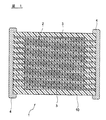
図1は本発明の一実施形態に係る積層セラミックコンデンサの断面図、
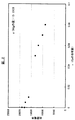
図2は主成分におけるCaの含有量と比誘電率との関係を示すグラフ、
図3は主成分におけるMgの含有量と比誘電率との関係を示すグラフ、
図4は主成分におけるMgの含有量とIR不良率との関係を示すグラフである。
Hereinafter, the present invention will be described based on embodiments shown in the drawings.
FIG. 1 is a cross-sectional view of a multilayer ceramic capacitor according to an embodiment of the present invention.
FIG. 2 is a graph showing the relationship between Ca content and relative dielectric constant in the main component,
FIG. 3 is a graph showing the relationship between the Mg content in the main component and the relative dielectric constant;
FIG. 4 is a graph showing the relationship between the Mg content in the main component and the IR defect rate.
図1に示すように、本発明の一実施形態に係る積層セラミックコンデンサ1は、誘電体層2と内部電極層3とが交互に積層された構成のコンデンサ素子本体10を有する。このコンデンサ素子本体10の両端部には、素子本体10の内部で交互に配置された内部電極層3と各々導通する一対の外部電極4が形成してある。コンデンサ素子本体10の形状に特に制限はないが、通常、直方体状とされる。また、その寸法にも特に制限はなく、用途に応じて適当な寸法とすればよい。
As shown in FIG. 1, a multilayer
内部電極層3は、各端面がコンデンサ素子本体10の対向する2端部の表面に交互に露出するように積層してある。一対の外部電極4は、コンデンサ素子本体10の両端部に形成され、交互に配置された内部電極層3の露出端面に接続されて、コンデンサ回路を構成する。
The
誘電体層2は、本発明の誘電体磁器組成物を含有する。
本発明の誘電体磁器組成物は、{{Ba(1−x)Cax}O}A{Ti(1−y−z)ZryMgz}BO2で表される組成の誘電体酸化物を含む主成分と、Mnの酸化物と、Yの酸化物と、Vの酸化物と、Siの酸化物とを含む副成分とを有する。この際、酸素(O)量は、上記式の化学量論組成から若干偏倚してもよい。
The
The dielectric ceramic composition of the present invention is a dielectric oxide having a composition represented by {{Ba (1-x) Ca x } O} A {Ti (1-yz) Zr y Mg z } B O 2. A main component including a substance, an oxide of Mn, an oxide of Y, an oxide of V, and a subcomponent including an oxide of Si. At this time, the amount of oxygen (O) may be slightly deviated from the stoichiometric composition of the above formula.
上記式中、xは、0.0001以上0.07以下、好ましくは0.0001以上0.05未満である。 In the above formula, x is 0.0001 or more and 0.07 or less, preferably 0.0001 or more and less than 0.05.
また、yは、0.1以上0.3以下、好ましくは0.15以上0.20以下である。 Moreover, y is 0.1 or more and 0.3 or less, preferably 0.15 or more and 0.20 or less.
また、zは、0.0005以上0.01以下、好ましくは0.003以上0.01以下である。 Z is 0.0005 or more and 0.01 or less, preferably 0.003 or more and 0.01 or less.
また、A/Bは、0.995以上1.020以下、好ましくは1.000以上1.015以下である。 A / B is 0.995 or more and 1.020 or less, preferably 1.000 or more and 1.015 or less.
この組成において、xはCaの比率を表し、zはMgの比率を表すが、本発明の誘電体磁器組成物の特徴点は、主成分中にMg原子を含有し、さらに上記式においてxとzの値、つまりCaの比率とMgの比率を上記所定の範囲内とする点である。すなわち、主成分中にMg原子を含有し、Caの比率とMgの比率を上記所定の範囲内とすることにより、セラミックコンデンサを薄層化した場合においても、IR不良率を低くすることができ、かつ比誘電率を高くすることが可能となる。 In this composition, x represents the ratio of Ca, and z represents the ratio of Mg. The feature of the dielectric ceramic composition of the present invention is that the main component contains Mg atoms, and in the above formula, x and The value of z, that is, the ratio of Ca and Mg is within the predetermined range. That is, when the main component contains Mg atoms and the ratio of Ca and Mg is within the predetermined range, the IR defect rate can be lowered even when the ceramic capacitor is thinned. In addition, the relative dielectric constant can be increased.
Caは、主に焼結安定性を向上させるとともに、絶縁抵抗値を向上させる元素として作用するものである。Caの比率を表すxが0.0001未満となると焼成時において、誘電体層の異常粒成長が生じ易くなる傾向にあり、xが0.07を超えると、比誘電率が低くなる傾向にある。従って、xの値は、0.0001≦x≦0.07の範囲が望ましく、比誘電率の向上という観点より、好ましくは0.0001≦x<0.05である。 Ca mainly acts as an element for improving the sintering stability and the insulation resistance value. When x representing the ratio of Ca is less than 0.0001, abnormal grain growth of the dielectric layer tends to occur during firing, and when x exceeds 0.07, the relative permittivity tends to decrease. . Therefore, the value of x is preferably in the range of 0.0001 ≦ x ≦ 0.07, and preferably 0.0001 ≦ x <0.05 from the viewpoint of improving the relative dielectric constant.
Mgは、IR不良率を低減させる元素として作用するものである。Mgの比率を表すzが0.0005未満となるとIR不良率が高くなる傾向にあり、zが0.01を超えると比誘電率が低くなる傾向にある。従って、zの値は、0.0005≦z≦0.01の範囲が望ましい。 Mg acts as an element that reduces the IR defect rate. When z representing the ratio of Mg is less than 0.0005, the IR defect rate tends to increase, and when z exceeds 0.01, the relative permittivity tends to decrease. Therefore, the value of z is preferably in the range of 0.0005 ≦ z ≦ 0.01.
前記組成式において、yはZrの比率を表し、このZrは、主にキュリー点を低温側に移動させるシフターとして作用するものである。yが0.1未満となると誘電損失が高くなる傾向にあり、また、yが0.3を超えると比誘電率が低くなる傾向にある。従って、yの値は0.1≦y≦0.3の範囲が望ましい。 In the composition formula, y represents the ratio of Zr, and this Zr mainly acts as a shifter that moves the Curie point to the low temperature side. When y is less than 0.1, the dielectric loss tends to increase, and when y exceeds 0.3, the relative permittivity tends to decrease. Therefore, the value of y is preferably in the range of 0.1 ≦ y ≦ 0.3.
前記組成式において、A/Bが0.995未満になると、焼成時に誘電体層の異常粒成長が生じ易くなると共に、絶縁抵抗値が低下する傾向にあり、A/Bが1.020を超えると焼結性が低下する傾向にあり、緻密な焼結体が得にくくなる。従って、A/Bは0.995≦A/B≦1.020の範囲が好ましい。 In the composition formula, when A / B is less than 0.995, abnormal grain growth of the dielectric layer tends to occur during firing, and the insulation resistance value tends to decrease, and A / B exceeds 1.020. And the sinterability tends to decrease, making it difficult to obtain a dense sintered body. Therefore, A / B is preferably in the range of 0.995 ≦ A / B ≦ 1.020.
前記Mnの酸化物は、焼結を促進する効果と、IRを高くする効果と、IR寿命を向上させる効果とがあり、主成分100モルに対して、MnO換算で0.03〜1.70モル、好ましくは、0.3〜1.4モルである。Mnの酸化物の含有量が少な過ぎると、添加した効果が得にくくなる傾向にあり、多過ぎると、比誘電率が低下する傾向にある。 The oxide of Mn has an effect of promoting sintering, an effect of increasing IR, and an effect of improving the IR lifetime, and is 0.03 to 1.70 in terms of MnO with respect to 100 mol of the main component. Mol, preferably 0.3 to 1.4 mol. If the Mn oxide content is too small, the added effect tends to be difficult to obtain, and if it is too much, the relative dielectric constant tends to decrease.
前記Yの酸化物は、主として、IR寿命を向上させる効果を示し、主成分100モルに対して、Y2O3換算で0.05〜0.5モル、好ましくは、0.085〜0.48モルである。Yの酸化物の含有量が少な過ぎると、このような効果が不十分となり、IR寿命が悪化してしまう傾向にあり、多過ぎると、焼結性が悪化する傾向にある。 The oxide of Y mainly exhibits an effect of improving the IR lifetime, and is 0.05 to 0.5 mol, preferably 0.085 to 0.005 in terms of Y 2 O 3 with respect to 100 mol of the main component. 48 moles. If the content of the oxide of Y is too small, such an effect is insufficient and the IR life tends to be deteriorated. If it is too much, the sinterability tends to be deteriorated.
前記Vの酸化物は、IR寿命を向上させる効果があり、主成分100モルに対して、V2O5換算で0.007〜0.4モル、好ましくは、0.01〜0.27モルである。Vの酸化物の含有量がが少な過ぎると、これらの効果が不十分となる傾向にあり、多過ぎると、IRが著しく低下する傾向にある。 The oxide of V has an effect of improving the IR lifetime, and is 0.007 to 0.4 mol, preferably 0.01 to 0.27 mol in terms of V 2 O 5 with respect to 100 mol of the main component. It is. When the content of V oxide is too small, these effects tend to be insufficient, and when it is too large, IR tends to be remarkably lowered.
前記Siの酸化物は、焼結助剤として作用し、主成分100モルに対して、SiO2換算で、0〜0.5モル、好ましくは、0〜0.4モルである。Siの酸化物の含有量が多過ぎると、比誘電率が低下する傾向にある。 The oxide of Si acts as a sintering aid, and is 0 to 0.5 mol, preferably 0 to 0.4 mol in terms of SiO 2 with respect to 100 mol of the main component. When the content of Si oxide is too large, the dielectric constant tends to decrease.
また、副成分として、Wの酸化物をさらに含むことが好ましい。Wの酸化物は、キュリー温度以上での容量温度特性を平坦化する効果と、IR寿命を向上させる効果とがあり、主成分100モルに対して、WO3換算で、好ましくは0.005〜0.3、さらに好ましくは0.01〜0.20モルである。Wの酸化物の含有量がが少な過ぎると、添加した効果が得にくくなる傾向にあり、多過ぎると、IRが著しく低下する傾向にある。 Moreover, it is preferable that the oxide of W is further included as a subcomponent. The oxide of W has the effect of flattening the capacity-temperature characteristics above the Curie temperature and the effect of improving the IR lifetime, and is preferably 0.005 in terms of WO 3 with respect to 100 mol of the main component. 0.3, more preferably 0.01 to 0.20 mol. When the content of the W oxide is too small, the added effect tends to be difficult to obtain, and when it is too large, the IR tends to be remarkably lowered.
なお、本明細書では、主成分および各副成分を構成する各酸化物を化学量論組成で表しているが、各酸化物の酸化状態は、化学量論組成から外れるものであってもよい。ただし、各副成分の上記比率は、各副成分を構成する酸化物に含有される金属量から上記化学量論組成の酸化物に換算して求める。 Note that, in this specification, each oxide constituting the main component and each subcomponent is represented by a stoichiometric composition, but the oxidation state of each oxide may be out of the stoichiometric composition. . However, the said ratio of each subcomponent is calculated | required by converting into the oxide of the said stoichiometric composition from the metal amount contained in the oxide which comprises each subcomponent.
誘電体層2の厚さは、特に限定されないが、一層あたり6.0μm以下であることが好ましく、より好ましくは4.5μm以下、特に好ましくは、3.5μm以下である。厚さの下限は、特に限定されないが、たとえば0.5μm程度である。
The thickness of the
誘電体層2の積層数は、特に限定されないが、20以上であることが好ましく、より好ましくは50以上、特に好ましくは、100以上である。積層数の上限は、特に限定されないが、たとえば2000程度である。
The number of laminated
本実施形態では、誘電体層2の厚みを、4.5μm以下に薄くした場合でも、IR不良率が低く、かつ高い比誘電率を有する積層セラミックコンデンサを得ることができる。
In the present embodiment, even when the thickness of the
誘電体層2に含まれる誘電体粒子の平均結晶粒径は、特に限定されないが、好ましくは、平均結晶粒径をR、誘電体層2の厚みをdとしたとき、平均結晶粒径Rと誘電体層の厚みdとの比(R/d)が、好ましくは0.5<R/d<3、さらに好ましくは0.5<R/d<1.5である。
The average crystal grain size of the dielectric particles contained in the
平均結晶粒径Rと誘電体層の厚みdとの比(R/d)が0.5以下となると比誘電率が低下する傾向にあり、3以上となるとIR不良率が高くなる傾向にある。 When the ratio (R / d) between the average crystal grain size R and the thickness d of the dielectric layer is 0.5 or less, the relative permittivity tends to decrease, and when it is 3 or more, the IR defect rate tends to increase. .
本実施形態のように、平均結晶粒径Rと誘電体層の厚みdとの比(R/d)を0.5<R/d<3とすることにより、電極間の誘電体粒子の数が1粒子または2粒子である部分の割合を増加することができ、積層セラミックコンデンサの体積当たりの静電容量を大きくすることが可能となる。なお、電極間の誘電体粒子の数とは、1本の内部電極から、その内部電極と対峙する内部電極に垂直に引いた直線が通る粒子の数を意味する。 As in this embodiment, by setting the ratio (R / d) of the average crystal grain size R to the thickness d of the dielectric layer to 0.5 <R / d <3, the number of dielectric particles between the electrodes It is possible to increase the ratio of the portion of which is one particle or two particles, and to increase the capacitance per volume of the multilayer ceramic capacitor. The number of dielectric particles between the electrodes means the number of particles passing through a straight line drawn perpendicularly from one internal electrode to the internal electrode facing the internal electrode.
内部電極層3に含有される導電材は特に限定されないが、誘電体層2の構成材料が耐還元性を有するため、卑金属を用いることができる。導電材として用いる卑金属としては、NiまたはNi合金が好ましい。Ni合金としては、Mn,Cr,CoおよびAlから選択される1種以上の元素とNiとの合金が好ましく、合金中のNi含有量は95重量%以上であることが好ましい。なお、NiまたはNi合金中には、P等の各種微量成分が0.1重量%程度以下含まれていてもよい。内部電極層3の厚さは用途等に応じて適宜決定すればよいが、通常、0.1〜3μm、特に0.2〜2.0μm程度であることが好ましい。
The conductive material contained in the
外部電極4に含有される導電材は特に限定されないが、本発明では安価なNi,Cuや、これらの合金を用いることができる。外部電極4の厚さは用途等に応じて適宜決定されればよいが、通常、10〜50μm程度であることが好ましい。
The conductive material contained in the
本発明の誘電体磁器組成物を用いた積層セラミックコンデンサは、従来の積層セラミックコンデンサと同様に、ペーストを用いた通常の印刷法やシート法によりグリーンチップを作製し、これを焼成した後、外部電極を印刷または転写して焼成することにより製造される。以下、製造方法について具体的に説明する。 In the multilayer ceramic capacitor using the dielectric ceramic composition of the present invention, as in the conventional multilayer ceramic capacitor, a green chip is produced by a normal printing method or sheet method using a paste, and this is fired, and then externally It is manufactured by printing or transferring an electrode and firing. Hereinafter, the manufacturing method will be specifically described.
まず、誘電体層用ペーストに含まれる誘電体磁器組成物粉末を準備し、これを塗料化して、誘電体層用ペーストを調整する。 First, the dielectric ceramic composition powder contained in the dielectric layer paste is prepared, and this is made into a paint to prepare the dielectric layer paste.
誘電体層用ペーストは、誘電体磁器組成物粉末と有機ビヒクルとを混練した有機系の塗料であってもよく、水系の塗料であってもよい。 The dielectric layer paste may be an organic paint obtained by kneading a dielectric ceramic composition powder and an organic vehicle, or may be a water-based paint.
誘電体磁器組成物粉末としては、上記した酸化物やその混合物、複合酸化物を用いることができるが、その他、焼成により上記した酸化物や複合酸化物となる各種化合物、例えば、炭酸塩、シュウ酸塩、硝酸塩、水酸化物、有機金属化合物等から適宜選択し、混合して用いることもできる。誘電体磁器組成物粉末中の各化合物の含有量は、焼成後に上記した誘電体磁器組成物の組成となるように決定すればよい。塗料化する前の状態で、誘電体磁器組成物粉末の粒径は、通常、平均粒径0.1〜1μm程度である。 As the dielectric ceramic composition powder, the above-described oxides, mixtures thereof, and composite oxides can be used. In addition, various compounds that become the above-described oxides and composite oxides by firing, such as carbonates and An acid salt, a nitrate, a hydroxide, an organometallic compound, or the like can be appropriately selected and mixed for use. What is necessary is just to determine content of each compound in a dielectric ceramic composition powder so that it may become a composition of the above-mentioned dielectric ceramic composition after baking. The particle size of the dielectric ceramic composition powder is usually about 0.1 to 1 [mu] m in average before the coating.
有機ビヒクルとは、バインダを有機溶剤中に溶解したものである。有機ビヒクルに用いるバインダは特に限定されず、エチルセルロース、ポリビニルブチラール等の通常の各種バインダから適宜選択すればよい。また、用いる有機溶剤も特に限定されず、印刷法やシート法など、利用する方法に応じて、テルピネオール、ブチルカルビトール、アセトン、トルエン等の各種有機溶剤から適宜選択すればよい。 An organic vehicle is obtained by dissolving a binder in an organic solvent. The binder used for the organic vehicle is not particularly limited, and may be appropriately selected from usual various binders such as ethyl cellulose and polyvinyl butyral. Further, the organic solvent to be used is not particularly limited, and may be appropriately selected from various organic solvents such as terpineol, butyl carbitol, acetone, toluene, and the like, depending on a method to be used such as a printing method or a sheet method.
また、誘電体層用ペーストを水系の塗料とする場合には、水溶性のバインダや分散剤などを水に溶解させた水系ビヒクルと、誘電体原料とを混練すればよい。水系ビヒクルに用いる水溶性バインダは特に限定されず、例えば、ポリビニルアルコール、セルロース、水溶性アクリル樹脂などを用いればよい。 Further, when the dielectric layer paste is used as a water-based paint, a water-based vehicle in which a water-soluble binder or a dispersant is dissolved in water and a dielectric material may be kneaded. The water-soluble binder used for the water-based vehicle is not particularly limited, and for example, polyvinyl alcohol, cellulose, water-soluble acrylic resin, or the like may be used.
内部電極層用ペーストは、上記した各種導電性金属や合金からなる導電材、あるいは焼成後に上記した導電材となる各種酸化物、有機金属化合物、レジネート等と、上記した有機ビヒクルとを混練して調製する。 The internal electrode layer paste is obtained by kneading the above-mentioned organic vehicle with various conductive metals and alloys as described above, or various oxides, organometallic compounds, resinates, etc. that become the above-mentioned conductive materials after firing. Prepare.
外部電極用ペーストは、上記した内部電極層用ペーストと同様にして調製すればよい。 The external electrode paste may be prepared in the same manner as the internal electrode layer paste described above.
上記した各ペースト中の有機ビヒクルの含有量に特に制限はなく、通常の含有量、例えば、バインダは1〜5重量%程度、溶剤は10〜50重量%程度とすればよい。また、各ペースト中には、必要に応じて各種分散剤、可塑剤、誘電体、絶縁体等から選択される添加物が含有されていてもよい。これらの総含有量は、10重量%以下とすることが好ましい。 There is no restriction | limiting in particular in content of the organic vehicle in each above-mentioned paste, For example, what is necessary is just about 1-5 weight% of binders, for example, about 10-50 weight% of binders. Each paste may contain additives selected from various dispersants, plasticizers, dielectrics, insulators, and the like as necessary. The total content of these is preferably 10% by weight or less.
印刷法を用いる場合、誘電体層用ペーストおよび内部電極層用ペーストを、PET等の基板上に積層印刷し、所定形状に切断した後、基板から剥離してグリーンチップとする。 When the printing method is used, the dielectric layer paste and the internal electrode layer paste are laminated and printed on a substrate such as PET, cut into a predetermined shape, and then peeled from the substrate to obtain a green chip.
また、シート法を用いる場合、誘電体層用ペーストを用いてグリーンシートを形成し、この上に内部電極層用ペーストを印刷した後、これらを積層してグリーンチップとする。 When the sheet method is used, a dielectric layer paste is used to form a green sheet, the internal electrode layer paste is printed thereon, and these are stacked to form a green chip.
焼成前に、グリーンチップに脱バインダ処理を施す。脱バインダ処理は、内部電極層ペースト中の導電材の種類に応じて適宜決定されればよいが、導電材としてNiやNi合金等の卑金属を用いる場合、脱バインダ雰囲気中の酸素分圧を10−45 〜105 Paとすることが好ましい。酸素分圧が前記範囲未満であると、脱バインダ効果が低下する。また酸素分圧が前記範囲を超えると、内部電極層が酸化する傾向にある。 Before firing, the green chip is subjected to binder removal processing. The binder removal treatment may be appropriately determined according to the type of the conductive material in the internal electrode layer paste. However, when a base metal such as Ni or Ni alloy is used as the conductive material, the oxygen partial pressure in the binder removal atmosphere is 10 It is preferable to be −45 to 10 5 Pa. When the oxygen partial pressure is less than the above range, the binder removal effect is lowered. If the oxygen partial pressure exceeds the above range, the internal electrode layer tends to oxidize.
また、それ以外の脱バインダ条件としては、昇温速度を好ましくは5〜300℃/時間、より好ましくは10〜100℃/時間、保持温度を好ましくは180〜400℃、より好ましくは200〜350℃、温度保持時間を好ましくは0.5〜24時間、より好ましくは2〜20時間とする。また、焼成雰囲気は、空気もしくは還元性雰囲気とすることが好ましく、還元性雰囲気における雰囲気ガスとしては、たとえばN2 とH2 との混合ガスを加湿して用いることが好ましい。 As other binder removal conditions, the temperature rising rate is preferably 5 to 300 ° C./hour, more preferably 10 to 100 ° C./hour, and the holding temperature is preferably 180 to 400 ° C., more preferably 200 to 350. The temperature holding time is preferably 0.5 to 24 hours, more preferably 2 to 20 hours. The firing atmosphere is preferably air or a reducing atmosphere, and as an atmosphere gas in the reducing atmosphere, for example, a mixed gas of N 2 and H 2 is preferably used after being humidified.
グリーンチップ焼成時の雰囲気は、内部電極層用ペースト中の導電材の種類に応じて適宜決定されればよいが、導電材としてNiやNi合金等の卑金属を用いる場合、焼成雰囲気中の酸素分圧は、10−9〜10−4Paとすることが好ましい。酸素分圧が前記範囲未満であると、内部電極層の導電材が異常焼結を起こし、途切れてしまうことがある。また、酸素分圧が前記範囲を超えると、内部電極層が酸化する傾向にある。 The atmosphere at the time of green chip firing may be appropriately determined according to the type of conductive material in the internal electrode layer paste, but when a base metal such as Ni or Ni alloy is used as the conductive material, the oxygen content in the firing atmosphere The pressure is preferably 10 −9 to 10 −4 Pa. When the oxygen partial pressure is less than the above range, the conductive material of the internal electrode layer may be abnormally sintered and may be interrupted. Further, when the oxygen partial pressure exceeds the above range, the internal electrode layer tends to be oxidized.
また、焼成時の保持温度は、好ましくは1100〜1400℃、より好ましくは1200〜1300℃である。保持温度が前記範囲未満であると緻密化が不十分となり、前記範囲を超えると、内部電極層の異常焼結による電極の途切れや、内部電極層構成材料の拡散による容量温度特性の悪化、誘電体磁器組成物の還元が生じやすくなる。 Moreover, the holding temperature at the time of baking becomes like this. Preferably it is 1100-1400 degreeC, More preferably, it is 1200-1300 degreeC. If the holding temperature is lower than the above range, the densification becomes insufficient. If the holding temperature is higher than the above range, the electrode temperature is interrupted due to abnormal sintering of the internal electrode layer, the capacity temperature characteristic deteriorates due to diffusion of the constituent material of the internal electrode layer, and the dielectric Reduction of the body porcelain composition is likely to occur.
これ以外の焼成条件としては、昇温速度を好ましくは50〜500℃/時間、より好ましくは200〜300℃/時間、温度保持時間を好ましくは0.5〜8時間、より好ましくは1〜3時間、冷却速度を好ましくは50〜500℃/時間、より好ましくは200〜300℃/時間とする。また、焼成雰囲気は還元性雰囲気とすることが好ましく、雰囲気ガスとしてはたとえば、N2 とH2 との混合ガスを加湿して用いることが好ましい。 As other firing conditions, the rate of temperature rise is preferably 50 to 500 ° C./hour, more preferably 200 to 300 ° C./hour, and the temperature holding time is preferably 0.5 to 8 hours, more preferably 1 to 3 hours. The time and cooling rate are preferably 50 to 500 ° C./hour, more preferably 200 to 300 ° C./hour. Further, the firing atmosphere is preferably a reducing atmosphere, and as the atmosphere gas, for example, a mixed gas of N 2 and H 2 is preferably used by humidification.
還元性雰囲気中で焼成した場合、コンデンサ素子本体にはアニールを施すことが好ましい。アニールは、誘電体層を再酸化するための処理であり、これによりIR寿命を著しく長くすることができるので、信頼性が向上する。 When firing in a reducing atmosphere, it is preferable to anneal the capacitor element body. Annealing is a process for re-oxidizing the dielectric layer, and this can significantly increase the IR lifetime, thereby improving the reliability.
アニール雰囲気中の酸素分圧は、10−3Pa以上、特に10−2〜10Paとすることが好ましい。酸素分圧が前記範囲未満であると誘電体層の再酸化が困難であり、前記範囲を超えると内部電極層が酸化する傾向にある。 The oxygen partial pressure in the annealing atmosphere is preferably 10 −3 Pa or more, particularly preferably 10 −2 to 10 Pa. When the oxygen partial pressure is less than the above range, it is difficult to reoxidize the dielectric layer, and when it exceeds the above range, the internal electrode layer tends to be oxidized.
アニールの際の保持温度は、1100℃以下、特に500〜1100℃とすることが好ましい。保持温度が前記範囲未満であると誘電体層の酸化が不十分となるので、IRが低く、また、IR寿命が短くなりやすい。一方、保持温度が前記範囲を超えると、内部電極層が酸化して容量が低下するだけでなく、内部電極層が誘電体素地と反応してしまい、容量温度特性の悪化、IRの低下、IR寿命の低下が生じやすくなる。なお、アニールは昇温過程および降温過程だけから構成してもよい。すなわち、温度保持時間を零としてもよい。この場合、保持温度は最高温度と同義である。 The holding temperature at the time of annealing is preferably 1100 ° C. or less, particularly 500 to 1100 ° C. When the holding temperature is lower than the above range, the dielectric layer is not sufficiently oxidized, so that the IR is low and the IR life tends to be short. On the other hand, if the holding temperature exceeds the above range, not only the internal electrode layer is oxidized and the capacity is lowered, but the internal electrode layer reacts with the dielectric substrate, the capacity temperature characteristic is deteriorated, the IR is lowered, the IR Life is likely to decrease. Note that annealing may be composed of only a temperature raising process and a temperature lowering process. That is, the temperature holding time may be zero. In this case, the holding temperature is synonymous with the maximum temperature.
これ以外のアニール条件としては、温度保持時間を好ましくは0〜20時間、より好ましくは2〜10時間、冷却速度を好ましくは50〜500℃/時間、より好ましくは100〜300℃/時間とする。また、アニールの雰囲気ガスとしては、たとえば、加湿したN2 ガス等を用いることが好ましい。 As other annealing conditions, the temperature holding time is preferably 0 to 20 hours, more preferably 2 to 10 hours, and the cooling rate is preferably 50 to 500 ° C./hour, more preferably 100 to 300 ° C./hour. . Further, as the annealing atmosphere gas, for example, humidified N 2 gas or the like is preferably used.
上記した脱バインダ処理、焼成およびアニールにおいて、N2 ガスや混合ガス等を加湿するには、例えばウェッター等を使用すればよい。この場合、水温は5〜75℃程度が好ましい。
脱バインダ処理、焼成およびアニールは、連続して行なっても、独立に行なってもよい。
In the above-described binder removal processing, firing and annealing, for example, a wetter or the like may be used to wet the N 2 gas or mixed gas. In this case, the water temperature is preferably about 5 to 75 ° C.
The binder removal treatment, firing and annealing may be performed continuously or independently.
上記のようにして得られたコンデンサ素子本体に、例えばバレル研磨やサンドブラストなどにより端面研磨を施し、外部電極用ペーストを印刷または転写して焼成し、外部電極4を形成する。外部電極用ペーストの焼成条件は、例えば、加湿したN2 とH2 との混合ガス中で600〜800℃にて10分間〜1時間程度とすることが好ましい。そして、必要に応じ、外部電極4表面に、めっき等により被覆層を形成する。
このようにして製造された本発明の積層セラミックコンデンサは、ハンダ付等によりプリント基板上などに実装され、各種電子機器等に使用される。
The capacitor element body obtained as described above is subjected to end surface polishing, for example, by barrel polishing or sand blasting, and the external electrode paste is printed or transferred and baked to form the
The multilayer ceramic capacitor of the present invention thus manufactured is mounted on a printed circuit board by soldering or the like and used for various electronic devices.
本発明によれば、主成分中にMg原子を含有し、さらに、主成分中のCaの比率とMgの比率を所定の範囲内とすることにより、セラミックコンデンサを薄層化した場合においても、IR不良率を低くすることができ、かつ比誘電率を高くすることができる。なお、誘電体磁器組成物を上記構成とすることにより、IR不良率が低下する原因の詳細については、判明していないが、主成分中にMg原子を添加することにより、誘電体磁器組成物の耐還元性が向上することが要因の一つとなっていると考えられる。 According to the present invention, when the ceramic capacitor is thinned by containing Mg atoms in the main component, and further, by making the ratio of Ca and the ratio of Mg in the main component within a predetermined range, The IR defect rate can be reduced and the relative dielectric constant can be increased. The details of the cause of the decrease in the IR defect rate due to the above-described configuration of the dielectric ceramic composition are not clarified, but by adding Mg atoms in the main component, the dielectric ceramic composition It is thought that one of the factors is that the reduction resistance of the product is improved.
以上、本発明の実施形態について説明してきたが、本発明は、上述した実施形態に何等限定されるものではなく、本発明の要旨を逸脱しない範囲内において種々に改変することができる。 As mentioned above, although embodiment of this invention has been described, this invention is not limited to the embodiment mentioned above at all, and can be variously modified within the range which does not deviate from the summary of this invention.
たとえば、上述した実施形態では、本発明に係る電子部品として積層セラミックコンデンサを例示したが、本発明に係る電子部品としては、積層セラミックコンデンサに限定されず、上記組成の誘電体磁器組成物で構成してある誘電体層を有するものであれば何でも良い。 For example, in the above-described embodiment, the multilayer ceramic capacitor is exemplified as the electronic component according to the present invention. However, the electronic component according to the present invention is not limited to the multilayer ceramic capacitor, and is composed of a dielectric ceramic composition having the above composition. Any material having a dielectric layer can be used.
以下、本発明を、さらに詳細な実施例に基づき説明するが、本発明は、これら実施例に限定されない。 Hereinafter, although this invention is demonstrated based on a more detailed Example, this invention is not limited to these Examples.
実施例1
主成分として、{Ba(1−x)Cax}O}A{Ti(1−y−z)ZryMgz}BO2で示される組成の誘電体酸化物を、組成比を示す記号x,zが、表1および2に示す値になるように、ゾルゲル合成により作製した。また、その他の記号A,B,yについては、A/B=0.989〜1.004、y=0.16とした。なお、本発明の範囲内である実施例の試料については、A/B=0.995〜1.004とした。
Example 1
As a main component, a {Ba (1-x) Ca x} O} A {Ti (1-y-z) Zr y Mg z} dielectric oxide having a composition represented by B O 2, the symbols indicating the composition ratio It was prepared by sol-gel synthesis so that x and z had values shown in Tables 1 and 2. For other symbols A, B, and y, A / B = 0.899 to 1.004 and y = 0.16. In addition, about the sample of the Example which is in the range of this invention, it was set as A / B = 0.995-1.004.
また、副成分として、主成分100モルに対して、MnO:0.4モルと、Y2O3:0.3モルと、V2O5:0.04モルと、WO3:0.08モルと、SiO2:0.8モルとを、ボールミルで20時間湿式粉砕し、900℃および4時間の条件で、大気雰囲気中で仮焼きし、その後、解砕のためにボールミルで20時間湿式粉砕し、副成分の添加物とした。
そして、主成分と副成分とを、ボールミルで19時間、湿式粉砕し、乾燥して、表1および2に示す試料番号1〜32の誘電体材料を得た。
Further, as subcomponents, MnO: 0.4 mol, Y 2 O 3 : 0.3 mol, V 2 O 5 : 0.04 mol, and WO 3 : 0.08 with respect to 100 mol of the main component. Mole and SiO 2 : 0.8 mol were wet-ground in a ball mill for 20 hours, calcined in the atmosphere at 900 ° C. for 4 hours, and then wet for 20 hours in a ball mill for crushing. This was pulverized and used as an additive of the accessory component.
And the main component and the subcomponent were wet-ground for 19 hours with a ball mill and dried to obtain dielectric materials of
これら試料番号1〜32の誘電体材料の各々を用いて、誘電体原料100重量部と、アクリル樹脂5.0重量部と、フタル酸ベンジルブチル2.5重量部と、ミネラルスピリット6.5重量部と、アセトン4.0重量部と、トリクロロエタン20.5重量部と塩化メチレン41.5重量部とをボールミルで混合し、ペースト化して誘電体層用ペーストを得た。 Using each of the dielectric materials of Sample Nos. 1 to 32, 100 parts by weight of dielectric material, 5.0 parts by weight of acrylic resin, 2.5 parts by weight of benzylbutyl phthalate, and 6.5 parts by weight of mineral spirits. Part, 4.0 parts by weight of acetone, 20.5 parts by weight of trichloroethane, and 41.5 parts by weight of methylene chloride were mixed by a ball mill and pasted to obtain a dielectric layer paste.
次に、Ni粒子44.6重量部と、テルピネオール52重量部と、エチルセルロース3重量部と、ベンゾトリアゾール0.4重量部とを、3本ロールにより混練し、スラリー化して内部電極層用ペーストを得た。 Next, 44.6 parts by weight of Ni particles, 52 parts by weight of terpineol, 3 parts by weight of ethyl cellulose, and 0.4 parts by weight of benzotriazole are kneaded with three rolls to form a slurry for an internal electrode layer paste. Obtained.
これらのペーストを用い、以下のようにして、図1に示される積層型セラミックチップコンデンサ1を製造した。
Using these pastes, the multilayer
得られた誘電体層用ペーストを用いてPETフィルム上にグリーンシートを形成した。この上に内部電極用ペーストを印刷した後、PETフィルムからシートを剥離した。次いで、これらのグリーンシートと保護用グリーンシート(内部電極層用ペーストを印刷しないもの)とを積層、圧着して、グリーンチップを得た。 Using the obtained dielectric layer paste, a green sheet was formed on a PET film. After the internal electrode paste was printed thereon, the sheet was peeled from the PET film. Next, these green sheets and protective green sheets (not printed with internal electrode layer paste) were laminated and pressure-bonded to obtain green chips.
得られた誘電体層用ペーストを用いてPETフィルム上にグリーンシートを形成した。この上に内部電極用ペーストを印刷した後、PETフィルムからシートを剥離した。次いで、これらのグリーンシートと保護用グリーンシート(内部電極層用ペーストを印刷しないもの)とを積層、圧着して、グリーンチップを得た。 Using the obtained dielectric layer paste, a green sheet was formed on a PET film. After the internal electrode paste was printed thereon, the sheet was peeled from the PET film. Next, these green sheets and protective green sheets (not printed with internal electrode layer paste) were laminated and pressure-bonded to obtain green chips.
次いで、グリーンチップを所定サイズに切断し、脱バインダ処理、焼成およびアニールを下記条件にて行って、積層セラミック焼成体を得た。脱バインダ処理条件は、昇温速度:30℃/時間、保持温度:260℃、温度保持時間:8時間、雰囲気:空気中とした。焼成条件は、昇温速度:200℃/時間、温度保持時間:2時間、冷却速度:300℃/時間、雰囲気ガス:加湿したN2 +H2 混合ガス(酸素分圧:10−2Pa)とした。なお、焼成時の保持温度は、表1および2に示した。アニール条件は、昇温速度:200℃/時間、保持温度:1000℃、温度保持時間:2時間、冷却速度:300℃/時間、雰囲気ガス:加湿したN2 ガス(酸素分圧:10−1Pa)とした。なお、焼成およびアニールの際の雰囲気ガスの加湿には、水温を5〜75℃としたウエッターを用いた。 Next, the green chip was cut into a predetermined size and subjected to binder removal processing, firing and annealing under the following conditions to obtain a multilayer ceramic fired body. The binder removal treatment conditions were temperature rising rate: 30 ° C./hour, holding temperature: 260 ° C., temperature holding time: 8 hours, and atmosphere: in the air. Firing conditions are: temperature rising rate: 200 ° C./hour, temperature holding time: 2 hours, cooling rate: 300 ° C./hour, atmospheric gas: humidified N 2 + H 2 mixed gas (oxygen partial pressure: 10 −2 Pa) did. The holding temperatures during firing are shown in Tables 1 and 2. The annealing conditions were as follows: temperature rising rate: 200 ° C./hour, holding temperature: 1000 ° C., temperature holding time: 2 hours, cooling rate: 300 ° C./hour, atmospheric gas: humidified N 2 gas (oxygen partial pressure: 10 −1 Pa). Note that a wetter with a water temperature of 5 to 75 ° C. was used for humidifying the atmospheric gas during firing and annealing.
次いで、得られた積層セラミック焼成体の端面をサンドブラストにて研磨した後、外部電極としてIn−Gaを塗布し、図1に示す積層セラミックコンデンサの試料1〜32を得た。
Next, after polishing the end face of the obtained multilayer ceramic fired body by sand blasting, In-Ga was applied as an external electrode, and
得られたコンデンサ試料のサイズは、3.2mm×1.6mm×0.6mmであり、内部電極層に挟まれた誘電体層の数は4とし、1層あたりの誘電体層の厚み(層間厚み)は3.0μmであり、内部電極層の厚さは1.2μmであった。また、各試料の誘電体層における平均結晶粒径を調べたところ、2.5μmであった。平均結晶粒径(R)と、前記誘電体層の厚み(d)との比(R/d)は0.83であった。 The size of the obtained capacitor sample was 3.2 mm × 1.6 mm × 0.6 mm, the number of dielectric layers sandwiched between internal electrode layers was 4, and the thickness of the dielectric layers per layer (interlayers) (Thickness) was 3.0 μm, and the thickness of the internal electrode layer was 1.2 μm. Further, when the average crystal grain size in the dielectric layer of each sample was examined, it was 2.5 μm. The ratio (R / d) between the average crystal grain size (R) and the thickness (d) of the dielectric layer was 0.83.
なお、誘電体層の厚さの測定方法としては、まず、得られたコンデンサ試料を内部電極に垂直な面で切断し、その切断面についてのSEM写真を撮影した。次に、SEM写真上で、内部電極と垂直な線を引き、該内部電極と対峙する隣の内部電極との距離を測定した。これを20回行い、その測定値の平均を求め、これを誘電体層の厚みとした。 As a method for measuring the thickness of the dielectric layer, first, the obtained capacitor sample was cut along a plane perpendicular to the internal electrode, and an SEM photograph of the cut surface was taken. Next, on the SEM photograph, a line perpendicular to the internal electrode was drawn, and the distance between the internal electrode and the adjacent internal electrode was measured. This was performed 20 times, and the average of the measured values was obtained, and this was taken as the thickness of the dielectric layer.
また、誘電体粒子の平均結晶粒径の測定方法としては、上記にて撮影したSEM写真から、コード法により誘電体粒子の形状を球と仮定して算出した。SEMの視野は23μm×30μmであり、1サンプルにつき80個の粒子について、それぞれの粒径を算出し、これの平均値を平均結晶粒径とした。
得られた各コンデンサ試料について下記に示す方法により、比誘電率およびIR不良率の測定を行った。
Moreover, as a method for measuring the average crystal grain size of the dielectric particles, it was calculated from the SEM photograph taken above, assuming that the shape of the dielectric particles was a sphere by the code method. The field of view of SEM is 23 μm × 30 μm, and the particle size of each of 80 particles per sample was calculated, and the average value thereof was taken as the average crystal particle size.
For each of the obtained capacitor samples, the relative dielectric constant and IR defect rate were measured by the method described below.
比誘電率(ε r )
コンデンサの試料に対し、基準温度20℃において、デジタルLCRメータ(YHP社製4274A)にて、周波数120Hz,入力信号レベル(測定電圧)1.0Vrms/μmの条件下で、静電容量Cおよび誘電損失tanδを測定した。そして、得られた静電容量から、比誘電率(単位なし)を算出した。
Dielectric constant (ε r )
Capacitor C and dielectric with respect to a capacitor sample under the conditions of a frequency of 120 Hz and an input signal level (measurement voltage) of 1.0 Vrms / μm using a digital LCR meter (YHP 4274A) at a reference temperature of 20 ° C. The loss tan δ was measured. Then, the relative dielectric constant (no unit) was calculated from the obtained capacitance.
比誘電率εrは、小型で高誘電率のコンデンサを作成するために重要な特性である。本実施例では、比誘電率εrの値は、コンデンサの試料数n=10個を用いて測定した値の平均値として算出した。比誘電率は、大きいほど好ましい。結果を表1および2に示す。 The relative dielectric constant ε r is an important characteristic for producing a small and high dielectric constant capacitor. In the present example, the value of the relative dielectric constant ε r was calculated as an average value of values measured using the number of capacitor samples n = 10. The relative dielectric constant is preferably as large as possible. The results are shown in Tables 1 and 2.
IR不良率
絶縁抵抗計(アドバンテスト社製R8340A)を用いて、20℃においてDC20Vを、コンデンサ試料に60秒間印加した後の絶縁抵抗IRを測定した。
測定した結果、絶縁抵抗IRが1.0×10¹⁰Ω以下となった試料を不良品とし、不良品の発生割合を%で示した。この値が小さいほど、IR不良率が低く、良品が多いこととなる。結果を表1および2に示す。
Using an IR defect rate insulation resistance meter (R8340A manufactured by Advantest Corporation), the insulation resistance IR after DC 20 V was applied to the capacitor sample for 60 seconds at 20 ° C. was measured.
As a result of the measurement, a sample having an insulation resistance IR of 1.0 × 10 10 Ω or less was regarded as a defective product, and the occurrence rate of the defective product was shown in%. The smaller this value, the lower the IR defect rate and the more non-defective products. The results are shown in Tables 1 and 2.

評価1
表1に、主成分を表す組成式{{Ba(1−x)Cax}O}A{Ti(1−y−z)ZryMgz}BO2(A/B=0.989〜1.004、y=0.16)において、xの値、すなわちCaの量と、zの値、すなわちMgの量を変化させた試料1〜33の組成比、焼成温度、比誘電率およびIR不良率を示した。なお、各試料について、比誘電率が10000以上で、かつIR不良率が50%未満となった試料を○、それ以外を×とし、あわせて表1に示した。
Table 1 shows a composition formula {{Ba (1-x) Ca x } O} A {Ti (1-yz) Zr y Mg z } B O 2 (A / B = 0.899- 1.004, y = 0.16), the composition ratio, firing temperature, relative dielectric constant, and IR of
また、図2に、zの値が0.003である試料15〜22について、xの値と比誘電率との関係を示した。 FIG. 2 shows the relationship between the value of x and the relative dielectric constant for samples 15 to 22 having a value of z of 0.003.
zの値をそれぞれ0.0005,0.001,0.003,0.01とした実施例および比較例の試料5〜29については、xの値を0.0001〜0.007の範囲内としたいずれの場合においても、IR不良率が0〜35%、比誘電率が10000以上となり、良好な結果となった。また、図2より、Mgの量を表すzの値を一定とした場合には、Caの量を表すxの値を増やしていくと、比誘電率が低下していくという関係があることがわかる。 For the samples 5 to 29 of Examples and Comparative Examples in which the value of z is 0.0005, 0.001, 0.003, and 0.01, respectively, the value of x is within the range of 0.0001 to 0.007. In either case, the IR defect rate was 0 to 35% and the relative dielectric constant was 10,000 or more, which was a favorable result. Further, from FIG. 2, when the value of z representing the amount of Mg is constant, there is a relationship that the relative permittivity decreases as the value of x representing the amount of Ca is increased. Understand.
一方、xの値を0とした比較例の試料9,15,23においては、焼成時に誘電体層の異常粒成長がみられ、xの値を0.08,0.2とした試料22,29は、比誘電率が10000未満となった。 On the other hand, in the samples 9, 15, and 23 of the comparative example in which the value of x is 0, abnormal grain growth of the dielectric layer is observed at the time of firing, and the samples 22 and 22 in which the value of x is 0.08 and 0.2. No. 29 has a relative dielectric constant of less than 10,000.
この結果より、zの値が、0.0005≦z≦0.01のとき、xの値は、0.0001≦x≦0.07、好ましくは0.0001≦x<0.05である場合に、IR不良率を低く抑えることができ、かつ高い比誘電率を有することが確認できた。 From this result, when the value of z is 0.0005 ≦ z ≦ 0.01, the value of x is 0.0001 ≦ x ≦ 0.07, preferably 0.0001 ≦ x <0.05. Furthermore, it was confirmed that the IR defect rate could be kept low and that the dielectric constant was high.
zの値を0または0.0001とした比較例の試料1〜4は、xの値をいずれの値としたときも、IR不良率が80%と高くなったり、焼成時に誘電体層の異常粒成長がみられた。この結果よりzの値は、0.0005以上であることが望ましいということが確認できた。 In Comparative Examples 1 to 4 in which the value of z is 0 or 0.0001, the IR defect rate becomes as high as 80% regardless of the value of x, or the dielectric layer is abnormal during firing. Grain growth was observed. From this result, it was confirmed that the value of z is preferably 0.0005 or more.
zの値を0.012または0.015とした比較例の試料30〜33は、xの値をいずれの値としたときも、比誘電率が10000未満となった。この結果よりzの値は、0.01以下であることが望ましいということが確認できた。 The comparative samples 30 to 33 in which the value of z was 0.012 or 0.015 had a relative dielectric constant of less than 10,000 when the value of x was any value. From this result, it was confirmed that the value of z is preferably 0.01 or less.
評価2
表2に、Caの量を表すxの値を一定値0.001とした試料の組成比、焼成温度、比誘電率およびIR不良率を示した。また、図3,4に、同様にxの値を一定値0.001とした試料について、zの値と比誘電率との関係(図3)およびzの値とIR不良率との関係(図4)を示した。
Table 2 shows the composition ratio, firing temperature, relative dielectric constant, and IR defect rate of a sample in which the value of x representing the amount of Ca is a constant value of 0.001. 3 and 4 similarly, the relationship between the value of z and the relative permittivity (FIG. 3) and the relationship between the value of z and the IR defect rate for the sample in which the value of x is a constant value of 0.001 ( FIG. 4) is shown.
Caの量を表すxの値を一定とした場合には、Mgの量を表すzの値を増していくと、図3に示すように、比誘電率が低下していくが、一方、IR不良率については、図4に示すように、改善されることが確認できた。また、表2に示すように、zの値を0.0005〜0.01とした実施例の試料は、比誘電率、IR不良率とも良好な結果となったが、zの値を0または、0.0001とした比較例の試料1,4は、IR不良率が80%と高くなってしまい、zの値を0.012または、0.015とした比較例31,33の試料は、比誘電率が10000以下となった。この結果より、zの値は、0.0005≦z≦0.01であり、好ましくは0.003≦z≦0.01である場合に、IR不良率を低く抑えることができ、かつ高い比誘電率を有することが確認できた。
When the value of x representing the amount of Ca is constant, as the value of z representing the amount of Mg increases, the relative permittivity decreases as shown in FIG. It was confirmed that the defect rate was improved as shown in FIG. Further, as shown in Table 2, the samples of the examples in which the value of z was 0.0005 to 0.01 showed good results in both the relative dielectric constant and the IR defect rate, but the value of z was 0 or
実施例2
副成分として、Wの酸化物であるWO3を添加しなかったこと以外は、実施例1と同様にして、表3に示す試料番号34〜41のコンデンサ試料を作製し、同様に、比誘電率およびIR不良率を測定した。
Example 2
A capacitor sample of sample numbers 34 to 41 shown in Table 3 was prepared in the same manner as in Example 1 except that WO 3 which is an oxide of W was not added as a subcomponent. The rate and IR failure rate were measured.
評価3
表3に、実施例2にて作製したコンデンサ試料34〜41の組成比、焼成温度、比誘電率およびIR不良率を示した。また、同様に各試料について、比誘電率が10000以上で、かつIR不良率が50%未満となった試料を○、それ以外を×とし、あわせて表3に示した。なお、実施例2の各試料においては、zの値、すなわちMgの量を一定とし、xの値、すなわちCaの量を変化させた。
Table 3 shows the composition ratio, firing temperature, relative dielectric constant, and IR defect rate of the capacitor samples 34 to 41 produced in Example 2. Similarly, for each sample, a sample having a relative dielectric constant of 10,000 or more and an IR defect rate of less than 50% is indicated by ◯, and other samples are indicated by ×. In each sample of Example 2, the value of z, that is, the amount of Mg was made constant, and the value of x, that is, the amount of Ca was changed.
表3より、副成分としてWの酸化物を含有しない実施例の試料35〜40は、xの値を0.0001〜0.007の範囲内としたいずれの場合においても、IR不良率が0%、比誘電率が10000以上となり、良好な結果となった。 From Table 3, the samples 35 to 40 of Examples not containing the oxide of W as a subcomponent have an IR defect rate of 0 in any case where the value of x is in the range of 0.0001 to 0.007. %, The relative dielectric constant was 10,000 or more, and good results were obtained.
一方、xの値を0とした比較例の試料34においては、焼成時に誘電体層の異常粒成長がみられ、xの値を0.08とした試料41は、比誘電率が10000未満となった。 On the other hand, in the sample 34 of the comparative example in which the value of x is 0, abnormal grain growth of the dielectric layer is observed during firing, and in the sample 41 in which the value of x is 0.08, the relative dielectric constant is less than 10,000. became.
この結果より、Wの酸化物を含有しない場合においても、誘電体層を薄層化した場合において、IR不良率を低く抑え、比誘電率を向上するという本発明の目的を達成することが可能であるということが確認できた。 As a result, even when the oxide of W is not contained, it is possible to achieve the object of the present invention to suppress the IR defect rate and improve the relative permittivity when the dielectric layer is thinned. It was confirmed that.
評価4
表4に、Wの酸化物を含有する試料16〜21、Wの酸化物を含有しない試料35〜40のxおよびzの値と、比誘電率を示した。
Table 4 shows values of x and z and relative dielectric constants of Samples 16 to 21 containing W oxide and Samples 35 to 40 not containing W oxide.
表4より、Wの酸化物を含有する場合も含有しない場合も、比誘電率については、ほぼ同様の結果となった。しかし、Wの酸化物を含有する試料16〜21は、IR寿命(高温負荷寿命)は、12時間であったが、Wの酸化物を含有しない試料35〜40は、IR寿命が10時間となり、Wの酸化物を含有しない場合は、IR寿命が短くなるという結果となった。 Table 4 shows that the relative permittivity was almost the same with and without the W oxide. However, samples 16 to 21 containing W oxide had an IR life (high temperature load life) of 12 hours, while samples 35 to 40 not containing W oxide had an IR life of 10 hours. When no W oxide was contained, the IR life was shortened.
なお、IR寿命(高温負荷寿命)は、誘電体層を薄層化する際に、特に重要となるものであり、IR寿命(高温負荷寿命)の測定方法としては、コンデンサ試料に対し、180℃で20V/μmの直流電圧の印加状態に保持することにより行った。本実施例では、直流電圧の印加開始から抵抗値が一桁落ちるまでの時間を寿命と定義し、これを10個のコンデンサ試料に対して行い、その平均値を寿命時間とした。 The IR life (high temperature load life) is particularly important when the dielectric layer is thinned. The IR life (high temperature load life) is measured at 180 ° C. with respect to the capacitor sample. This was carried out by maintaining a DC voltage application state of 20 V / μm. In this example, the time from the start of application of the DC voltage to the drop of the resistance value by one digit was defined as the lifetime, and this was performed for 10 capacitor samples, and the average value was defined as the lifetime.
この結果より、Wの酸化物を含有しない場合においても、本発明の目的を達成することが可能であるが、IR寿命(高温負荷寿命)を向上させ、さらに信頼性の高い積層セラミックコンデンサを得るためには、副成分としてWの酸化物を含有することが好ましいということが確認できた。 From this result, it is possible to achieve the object of the present invention even when no W oxide is contained, but the IR life (high temperature load life) is improved and a more reliable multilayer ceramic capacitor is obtained. Therefore, it was confirmed that it is preferable to contain an oxide of W as a subcomponent.
本実施例で示したように、誘電体層を4.5μm以下、特に3.0μm以下と薄層化した場合においても、主成分中にMg原子を含有し、Caの比率とMgの比率を上記所定の範囲内とすることにより、IR不良率が低く、比誘電率の高い積層セラミックコンデンサが得られることが確認できた。 As shown in this example, even when the dielectric layer is thinned to 4.5 μm or less, particularly 3.0 μm or less, it contains Mg atoms in the main component, and the ratio of Ca to the ratio of Mg is It was confirmed that a monolithic ceramic capacitor having a low IR defect rate and a high relative dielectric constant can be obtained by setting it within the predetermined range.
1… 積層セラミックコンデンサ
10… コンデンサ素子本体
2… 誘電体層
3… 内部電極層
4… 外部電極
DESCRIPTION OF
Claims (8)
(ただし、A,B,x,y,zが、0.995≦A/B≦1.020、0.0001≦x≦0.07、0.1≦y≦0.3、0.0005≦z≦0.01)
で表される主成分と、
副成分として、主成分100モルに対して、Mnの酸化物をMnO換算で0.03〜1.7モルと、Yの酸化物をY2O3換算で0.05〜0.5モルと、Vの酸化物をV2O5換算で0.007〜0.4モルと、Siの酸化物をSiO2換算で0〜0.5モルとを含有することを特徴とする誘電体磁器組成物。 Compositional Formula {{Ba (1-x) Ca x } O} A {Ti (1-y-z) Zr y Mg z } B O 2
(However, A, B, x, y, z are 0.995 ≦ A / B ≦ 1.020, 0.0001 ≦ x ≦ 0.07, 0.1 ≦ y ≦ 0.3, 0.0005 ≦ z ≦ 0.01)
A main component represented by
As subcomponents, the oxide of Mn is 0.03 to 1.7 mol in terms of MnO and the oxide of Y is 0.05 to 0.5 mol in terms of Y 2 O 3 with respect to 100 mol of the main component. A dielectric ceramic composition comprising 0.007 to 0.4 mol of V oxide in terms of V 2 O 5 and 0 to 0.5 mol of Si oxide in terms of SiO 2 Stuff.
The ratio (R / d) of the average crystal grain size (R) of the dielectric particles constituting the dielectric layer to the thickness (d) of the dielectric layer is 0.5 <R / d <3. The multilayer ceramic capacitor according to claim 4, wherein the multilayer ceramic capacitor is a multilayer ceramic capacitor.
Priority Applications (6)
| Application Number | Priority Date | Filing Date | Title |
|---|---|---|---|
| JP2003340577A JP2005104770A (en) | 2003-09-30 | 2003-09-30 | Dielectric ceramic composition and electronic component |
| TW093129213A TWI244098B (en) | 2003-09-30 | 2004-09-27 | Dielectric ceramic compositions and electronic devices |
| US10/951,941 US6995968B2 (en) | 2003-09-30 | 2004-09-29 | Dielectric ceramic compositions and electronic devices |
| CNB2004100874755A CN100483577C (en) | 2003-09-30 | 2004-09-30 | Dielectric ceramic compositions and electronic devices |
| KR1020040077840A KR100651019B1 (en) | 2003-09-30 | 2004-09-30 | dielectric ceramic compositions and electronic devices |
| EP04023367A EP1520844A3 (en) | 2003-09-30 | 2004-09-30 | Dielectric ceramic compositions and electronic devices |
Applications Claiming Priority (1)
| Application Number | Priority Date | Filing Date | Title |
|---|---|---|---|
| JP2003340577A JP2005104770A (en) | 2003-09-30 | 2003-09-30 | Dielectric ceramic composition and electronic component |
Publications (1)
| Publication Number | Publication Date |
|---|---|
| JP2005104770A true JP2005104770A (en) | 2005-04-21 |
Family
ID=34309051
Family Applications (1)
| Application Number | Title | Priority Date | Filing Date |
|---|---|---|---|
| JP2003340577A Pending JP2005104770A (en) | 2003-09-30 | 2003-09-30 | Dielectric ceramic composition and electronic component |
Country Status (6)
| Country | Link |
|---|---|
| US (1) | US6995968B2 (en) |
| EP (1) | EP1520844A3 (en) |
| JP (1) | JP2005104770A (en) |
| KR (1) | KR100651019B1 (en) |
| CN (1) | CN100483577C (en) |
| TW (1) | TWI244098B (en) |
Families Citing this family (13)
| Publication number | Priority date | Publication date | Assignee | Title |
|---|---|---|---|---|
| JP4777605B2 (en) * | 2003-05-21 | 2011-09-21 | 日本碍子株式会社 | Multi-layer piezoelectric / electrostrictive element |
| JP2006005222A (en) * | 2004-06-18 | 2006-01-05 | Tdk Corp | Ceramic electronic component and its manufacturing method |
| ATE519718T1 (en) * | 2004-07-08 | 2011-08-15 | Murata Manufacturing Co | DIELECTRIC CERAMIC COMPOSITION AND CERAMIC LAYER CAPACITOR |
| US7923395B2 (en) * | 2005-04-07 | 2011-04-12 | Kemet Electronics Corporation | C0G multi-layered ceramic capacitor |
| US20060229188A1 (en) * | 2005-04-07 | 2006-10-12 | Randall Michael S | C0G multi-layered ceramic capacitor |
| JP2007131476A (en) * | 2005-11-09 | 2007-05-31 | Tdk Corp | Dielectric ceramic composition, electronic component and multilayer ceramic capacitor |
| JP5046699B2 (en) * | 2007-03-27 | 2012-10-10 | 京セラ株式会社 | Dielectric porcelain and multilayer ceramic capacitor |
| JP5272754B2 (en) * | 2008-02-05 | 2013-08-28 | Tdk株式会社 | Dielectric porcelain composition and electronic component |
| JP2010226038A (en) * | 2009-03-25 | 2010-10-07 | Tdk Corp | Ceramic electronic component |
| KR101792368B1 (en) * | 2015-12-24 | 2017-11-20 | 삼성전기주식회사 | Dielectric ceramic composition, dielectric material and multilayer ceramic capacitor comprising the same |
| KR102166127B1 (en) * | 2015-12-28 | 2020-10-15 | 삼성전기주식회사 | Dielectric composition and multilayer ceramic capacitor comprising the same |
| KR20190116131A (en) | 2019-07-10 | 2019-10-14 | 삼성전기주식회사 | Multilayered capacitor and board having the same mounted thereon |
| CN116635348A (en) * | 2020-09-10 | 2023-08-22 | 基美电子公司 | Dielectric ceramic composition and ceramic capacitor using the same |
Family Cites Families (16)
| Publication number | Priority date | Publication date | Assignee | Title |
|---|---|---|---|---|
| JP3207847B2 (en) | 1989-10-18 | 2001-09-10 | ティーディーケイ株式会社 | Multilayer ceramic chip capacitors |
| US5319517A (en) * | 1992-03-27 | 1994-06-07 | Tdk Corporation | Multilayer ceramic chip capacitor |
| JP2787746B2 (en) | 1992-03-27 | 1998-08-20 | ティーディーケイ株式会社 | Multilayer ceramic chip capacitors |
| JP3269903B2 (en) | 1993-12-29 | 2002-04-02 | 太陽誘電株式会社 | Porcelain capacitor and method of manufacturing the same |
| KR0170577B1 (en) * | 1994-12-19 | 1999-01-15 | 무라따 야스따까 | Dielectric porcelain composition and laminated ceramic capacitor using the same |
| JPH09315861A (en) | 1996-05-30 | 1997-12-09 | Kyocera Corp | Dielectric ceramics composition |
| JP3039417B2 (en) * | 1997-02-07 | 2000-05-08 | 株式会社村田製作所 | Multilayer ceramic capacitors |
| JP3370933B2 (en) | 1998-05-01 | 2003-01-27 | 太陽誘電株式会社 | Multilayer ceramic capacitors |
| JP2001230148A (en) | 2000-02-16 | 2001-08-24 | Taiyo Yuden Co Ltd | Laminated ceramic capacitor and method of manufacturing it |
| TW492017B (en) * | 2000-06-29 | 2002-06-21 | Tdk Corp | Dielectrics porcelain composition and electronic parts |
| JP2002029835A (en) | 2000-07-13 | 2002-01-29 | Matsushita Electric Ind Co Ltd | Dielectric porcelain composition, laminated ceramic capacitor using the same and method for manufacturing that capacitor |
| JP2002187770A (en) * | 2000-12-15 | 2002-07-05 | Toho Titanium Co Ltd | Dielectric porcelain composition and laminated ceramic capacitor using the same |
| DE60232958D1 (en) * | 2001-04-12 | 2009-08-27 | Tdk Corp | PRODUCTION PROCESS FOR A CERAMIC ELECTRONIC MULTILAYER COMPONENT |
| JP4446324B2 (en) | 2001-09-27 | 2010-04-07 | 株式会社村田製作所 | Dielectric porcelain composition and capacitor using the same |
| KR100466073B1 (en) * | 2002-05-24 | 2005-01-13 | 삼성전기주식회사 | Dielectric Composition Having Improved Homogeneity And Insulation Resistance, Preparing Method Thereof And Multilayer Ceramic Condenser Using The Same |
| KR100466072B1 (en) * | 2002-05-24 | 2005-01-13 | 삼성전기주식회사 | Dielectric Composition For Multilayer Ceramic Condenser And Multilayer Ceramic Condenser Using The Same |
-
2003
- 2003-09-30 JP JP2003340577A patent/JP2005104770A/en active Pending
-
2004
- 2004-09-27 TW TW093129213A patent/TWI244098B/en not_active IP Right Cessation
- 2004-09-29 US US10/951,941 patent/US6995968B2/en not_active Expired - Lifetime
- 2004-09-30 KR KR1020040077840A patent/KR100651019B1/en active IP Right Grant
- 2004-09-30 CN CNB2004100874755A patent/CN100483577C/en not_active Expired - Lifetime
- 2004-09-30 EP EP04023367A patent/EP1520844A3/en not_active Withdrawn
Also Published As
| Publication number | Publication date |
|---|---|
| TW200522101A (en) | 2005-07-01 |
| CN100483577C (en) | 2009-04-29 |
| EP1520844A3 (en) | 2009-04-29 |
| KR20050031994A (en) | 2005-04-06 |
| KR100651019B1 (en) | 2006-11-29 |
| US20050111163A1 (en) | 2005-05-26 |
| US6995968B2 (en) | 2006-02-07 |
| CN1604247A (en) | 2005-04-06 |
| TWI244098B (en) | 2005-11-21 |
| EP1520844A2 (en) | 2005-04-06 |
Similar Documents
| Publication | Publication Date | Title |
|---|---|---|
| JP3908715B2 (en) | Multilayer ceramic capacitor | |
| JP4295179B2 (en) | Electronic component and manufacturing method thereof | |
| JP5275918B2 (en) | Multilayer ceramic electronic components | |
| JP4839913B2 (en) | Electronic component, dielectric ceramic composition and method for producing the same | |
| JP5018604B2 (en) | Dielectric porcelain composition and electronic component | |
| JP2005145791A (en) | Electronic components, dielectric porcelain composition, and method for manufacturing the same | |
| KR101358488B1 (en) | Dielectric ceramic composition and electronic device | |
| KR101272286B1 (en) | Dielectric ceramic composition and electronic device | |
| CN113321501A (en) | Dielectric composition and laminated electronic component | |
| JP4622537B2 (en) | Dielectric porcelain composition and electronic component | |
| JP4863005B2 (en) | Dielectric porcelain composition and electronic component | |
| JP4461679B2 (en) | Dielectric porcelain composition and electronic component | |
| KR100651019B1 (en) | dielectric ceramic compositions and electronic devices | |
| JP4403705B2 (en) | Dielectric porcelain composition and electronic component | |
| JP5017792B2 (en) | Electronic component, dielectric ceramic composition and method for producing the same | |
| JP4576807B2 (en) | Dielectric porcelain composition and electronic component | |
| JP4206062B2 (en) | Ceramic electronic component and manufacturing method thereof | |
| JP4556924B2 (en) | Dielectric porcelain composition and electronic component | |
| JP4661203B2 (en) | Ceramic electronic component and manufacturing method thereof | |
| JP2008227093A (en) | Manufacturing method of multilayer electronic component | |
| JP2007063040A (en) | Method for producing dielectric porcelain composition, and electronic component | |
| JP2008162862A (en) | Dielectric porcelain composition and electronic component | |
| JP4547945B2 (en) | Electronic component, dielectric ceramic composition and method for producing the same | |
| JP4696891B2 (en) | Electronic component, dielectric ceramic composition and method for producing the same | |
| JP2008174434A (en) | Dielectric porcelain composition and electronic component |
Legal Events
| Date | Code | Title | Description |
|---|---|---|---|
| A977 | Report on retrieval |
Free format text: JAPANESE INTERMEDIATE CODE: A971007 Effective date: 20071119 |
|
| A131 | Notification of reasons for refusal |
Free format text: JAPANESE INTERMEDIATE CODE: A131 Effective date: 20071127 |
|
| A601 | Written request for extension of time |
Free format text: JAPANESE INTERMEDIATE CODE: A601 Effective date: 20080125 |
|
| A521 | Request for written amendment filed |
Free format text: JAPANESE INTERMEDIATE CODE: A523 Effective date: 20080128 |
|
| A602 | Written permission of extension of time |
Free format text: JAPANESE INTERMEDIATE CODE: A602 Effective date: 20080130 |
|
| A02 | Decision of refusal |
Free format text: JAPANESE INTERMEDIATE CODE: A02 Effective date: 20081216 |