JP2005079210A - Thermoelectric converter - Google Patents
Thermoelectric converter Download PDFInfo
- Publication number
- JP2005079210A JP2005079210A JP2003305543A JP2003305543A JP2005079210A JP 2005079210 A JP2005079210 A JP 2005079210A JP 2003305543 A JP2003305543 A JP 2003305543A JP 2003305543 A JP2003305543 A JP 2003305543A JP 2005079210 A JP2005079210 A JP 2005079210A
- Authority
- JP
- Japan
- Prior art keywords
- heat
- insulating substrate
- heat absorption
- side insulating
- metal plate
- Prior art date
- Legal status (The legal status is an assumption and is not a legal conclusion. Google has not performed a legal analysis and makes no representation as to the accuracy of the status listed.)
- Granted
Links
Images


Landscapes
- Cooling Or The Like Of Semiconductors Or Solid State Devices (AREA)
Abstract
【課題】 熱抵抗が小さくかつ熱応力による不具合を効果的に防止し得る熱電変換装置を提供すること。
【解決手段】 吸熱側絶縁基板20及び/又は放熱側絶縁基板30の他方面20b、30bに、複数の金属板を各々離間して配設する。その上に冷却(加熱対象物)を金属接合することにより、接合部で発生する熱応力を効果的に分散させ、破損の防止に寄与し得る。また、吸熱側金属板41の配設パターンを放熱側電極14の配設パターンとし、放熱側金属板51の配設パターンを吸熱側電極12の配設パターンとすることにより、両基板及びそれに配設される金属板、電極を共通化することができる。
【選択図】 図1PROBLEM TO BE SOLVED: To provide a thermoelectric conversion device having a small thermal resistance and capable of effectively preventing problems due to thermal stress.
SOLUTION: A plurality of metal plates are arranged on the other surfaces 20b and 30b of the heat absorption side insulating substrate 20 and / or the heat radiation side insulating substrate 30 so as to be separated from each other. On top of that, cooling (heating object) is metal-bonded to effectively disperse the thermal stress generated at the joint, thereby contributing to prevention of breakage. Further, the arrangement pattern of the heat absorption side metal plate 41 is used as the arrangement pattern of the heat dissipation side electrode 14 and the arrangement pattern of the heat dissipation side metal plate 51 is used as the arrangement pattern of the heat absorption side electrode 12, so A common metal plate and electrode can be used.
[Selection] Figure 1
Description
この出願の発明は、ペルチェ効果又はゼーベック効果を利用した温調装置等の熱電変換装置に関するものであり、特に、温度差によって発生する熱応力を緩和する技術に係るものである。 The invention of this application relates to a thermoelectric conversion device such as a temperature control device using the Peltier effect or Seebeck effect, and particularly relates to a technique for alleviating thermal stress generated by a temperature difference.
ペルチェ効果を利用した熱電変換装置は、複数のN型熱電素子とP型熱電素子とを電極で順次連結し、通電することにより、N型熱電素子からP型熱電素子へと電流を流す際に両者の間に配設される電極(吸熱側電極)側で吸熱し、P型熱電素子からN型熱電素子へと電流を流す際に両者の間に配設される電極(放熱側電極)側で放熱するものである。このような構成の熱電変換装置において、吸熱効率又は放熱効率を向上させるために、放熱側電極を一方の側に集め、吸熱側電極を他方の側に集めてユニット化した構造が採られている。一般的には、放熱側絶縁基板の一方面に放熱側電極を配設するとともに吸熱側絶縁基板の一方面に吸熱側電極を配設させ、且つ、両基板の一方面を対向して配置させた構造が採用される。 A thermoelectric conversion device using the Peltier effect is configured to cause a current to flow from an N-type thermoelectric element to a P-type thermoelectric element by sequentially connecting and energizing a plurality of N-type thermoelectric elements and P-type thermoelectric elements. The electrode (heat-dissipation-side electrode) side that absorbs heat on the electrode (heat-absorption-side electrode) side disposed between the two and passes current from the P-type thermoelectric element to the N-type thermoelectric element Radiates heat. In the thermoelectric converter having such a configuration, in order to improve the heat absorption efficiency or the heat dissipation efficiency, a structure is adopted in which the heat dissipation side electrode is collected on one side and the heat absorption side electrode is collected on the other side to form a unit. . Generally, a heat-dissipation-side electrode is disposed on one surface of the heat-dissipation-side insulating substrate, a heat-absorption-side electrode is disposed on one surface of the heat-absorption-side insulating substrate, and one surface of both substrates is disposed opposite to each other. Structure is adopted.
熱電変換装置を利用して物体を冷却又は低温で温度調節しようとする場合には、吸熱側絶縁基板に冷却・温調対象物を熱的に接触させて冷却又は温調を行うが、吸熱側絶縁基板と冷却対象物とを接合する際に、樹脂性の接着剤等で両者を接合すると熱抵抗が増大し、冷却効率が低下する。よって、冷却効率を損なわずに冷却対象物を吸熱側絶縁基板に接合する手段として、吸熱側絶縁基板の他方面に金属薄膜あるいは金属板を配設して金属面を形成し、この金属面と冷却対象物とを半田付けや銅ろう、銀ろう等の金属接合により接合する手段が採られている。尚、このような金属面を、一般的にはメタライズ面と呼ぶ(非特許文献1のP.40参照)。このような構成を採ることにより、樹脂などの熱抵抗の高い材質を介さずに冷却対象物と吸熱側絶縁基板とを熱的に接触させることができるため、冷却効率を損なうことがないというものである。 When using an thermoelectric converter to cool an object or to adjust the temperature at a low temperature, the object to be cooled / temperature-controlled is brought into thermal contact with the insulating substrate on the heat-absorption side to cool or adjust the temperature. When the insulating substrate and the object to be cooled are bonded, if the both are bonded with a resinous adhesive or the like, the thermal resistance increases and the cooling efficiency decreases. Therefore, as a means for bonding the object to be cooled to the heat absorption side insulating substrate without impairing the cooling efficiency, a metal thin film or a metal plate is disposed on the other surface of the heat absorption side insulating substrate to form a metal surface. Means for joining the object to be cooled by soldering, metal joining such as copper brazing or silver brazing is employed. Such a metal surface is generally called a metallized surface (see page 40 of Non-Patent Document 1). By adopting such a configuration, the cooling target and the heat absorption side insulating substrate can be brought into thermal contact without using a material having high thermal resistance such as resin, so that the cooling efficiency is not impaired. It is.
しかしながら、上記したようなメタライズ面に金属接合により冷却対象物を接合するタイプの熱電変換装置では、発生する温度差によって各材質の線膨張係数の差に起因した熱応力が各接合部にかかり、特に金属接合の部分では熱応力を十分吸収することができずに装置が破損する可能性があるといった問題がある。 However, in the thermoelectric conversion device of the type that joins the object to be cooled by metal bonding to the metallized surface as described above, the thermal stress due to the difference in linear expansion coefficient of each material is applied to each joint due to the generated temperature difference, In particular, there is a problem that the device may be damaged because the thermal stress cannot be sufficiently absorbed at the metal bonded portion.
上記問題を解消するため、絶縁基板を無くしたスケルトン構造の熱電変換装置が提案されている(例えば、非特許文献1のP.41,図3.2参照)。スケルトン構造の熱電変換装置は、吸熱面又は放熱面が吸熱側電極又は放熱側電極自体となっているため、金属で作製される電極に対して特に線膨張係数の差が大きい絶縁基板を廃止することができ、さらに冷却対象物と電極との接合については、各電極に応力が分散される結果、応力緩和が図れるというものである。 In order to solve the above problem, a thermoelectric conversion device having a skeleton structure without an insulating substrate has been proposed (see, for example, P.41 of Non-Patent Document 1, FIG. 3.2). In the skeleton-structured thermoelectric conversion device, the heat absorption surface or heat dissipation surface is the heat absorption side electrode or the heat dissipation side electrode itself, so that the insulating substrate having a particularly large difference in linear expansion coefficient with respect to the electrode made of metal is eliminated. Further, with respect to the bonding between the object to be cooled and the electrode, the stress is dispersed as a result of the stress being dispersed in each electrode.
また、熱電変換装置内に応力緩和層を配設し、これによって熱応力を緩和するものも提案されている(例えば、特許文献1参照)。
しかしながら、非特許文献1に記載のスケルトン構造の熱電変換装置では、剥き出しの電極間の絶縁を確実に行うため、絶縁層を設けたりグリース層を厚くしたりするなどの処置が必要であり、このような絶縁層やグリース層の存在によって熱抵抗が大きくなってしまうといった問題がある。 However, in the thermoelectric conversion device having the skeleton structure described in Non-Patent Document 1, in order to reliably insulate the exposed electrodes, it is necessary to take measures such as providing an insulating layer or increasing the thickness of the grease layer. There is a problem that the thermal resistance increases due to the presence of such an insulating layer and a grease layer.
また、特許文献1に記載の応力緩和層を設けた熱電変換装置では、応力緩和層が一般的に樹脂で形成されるため、斯かる樹脂層の存在のためにやはり熱抵抗が大きくなってしまうといった問題がある。 Further, in the thermoelectric conversion device provided with the stress relaxation layer described in Patent Document 1, since the stress relaxation layer is generally formed of a resin, the thermal resistance is also increased due to the presence of the resin layer. There is a problem.
つまり、いずれの方法でも、絶縁処理又は熱応力緩和処理を施すために樹脂などの熱抵抗の大きな材質を介在させてしまっているため、冷却効率が低下してしまう。 That is, in any method, since a material having a large thermal resistance such as a resin is interposed in order to perform the insulating process or the thermal stress relaxation process, the cooling efficiency is lowered.
ゆえに、本発明は、上記実情に鑑みて成されたものであり、熱抵抗が小さくかつ熱応力による不具合を効果的に防止し得る熱電変換装置を提供することを、技術的課題とするものである。 Therefore, the present invention has been made in view of the above circumstances, and it is a technical problem to provide a thermoelectric conversion device that has a low thermal resistance and can effectively prevent problems due to thermal stress. is there.
上記技術的課題を解決するためになされた請求項1の発明は、
N型半導体材料からなる複数のN型熱電素子と、P型半導体材料からなる複数のP型熱電素子と、金属材料で形成された複数の放熱側電極及び吸熱側電極とを備え、N型熱電素子、吸熱側電極、P型熱電素子、放熱側電極をこの順で電気的に接続させてなる熱電変換手段と、
一方面に前記複数の吸熱側電極が配設された吸熱側絶縁基板と、
一方面に前記複数の放熱側電極が配設された放熱側絶縁基板とを有する熱電変換装置において、
前記吸熱側絶縁基板及び/又は前記放熱側絶縁基板の他方面には、複数の金属板が各々離間して配設されてなることを特徴とする、熱電変換装置としたことである。
The invention of claim 1 made to solve the above technical problem is:
A plurality of N-type thermoelectric elements made of an N-type semiconductor material; a plurality of P-type thermoelectric elements made of a P-type semiconductor material; and a plurality of heat radiation side electrodes and heat absorption side electrodes made of a metal material, Thermoelectric conversion means in which the element, the heat absorption side electrode, the P-type thermoelectric element, and the heat radiation side electrode are electrically connected in this order;
A heat-absorbing-side insulating substrate having the plurality of heat-absorbing-side electrodes disposed on one surface;
In the thermoelectric conversion device having a heat radiation side insulating substrate on which one of the plurality of heat radiation side electrodes is disposed,
The thermoelectric conversion device is characterized in that a plurality of metal plates are disposed separately on the other surface of the heat absorption side insulating substrate and / or the heat radiation side insulating substrate.
また、請求項2の発明は、請求項1の発明において、
前記吸熱側絶縁基板の一方面に配設された前記吸熱側電極の配設パターンは、前記放熱側絶縁基板の他方面に配設された前記金属板の配設パターンと同一であり、
前記放熱側絶縁基板の一方面に配設された前記放熱側電極の配設パターンは、前記吸熱側絶縁基板の他方面に配設された前記金属板の配設パターンと同一であることを特徴としている。
The invention of claim 2 is the invention of claim 1,
The arrangement pattern of the heat absorption side electrode arranged on one surface of the heat absorption side insulating substrate is the same as the arrangement pattern of the metal plate arranged on the other surface of the heat radiation side insulating substrate,
The disposition pattern of the heat dissipating side electrode disposed on one surface of the heat dissipating side insulating substrate is the same as the disposition pattern of the metal plate disposed on the other surface of the heat absorbing side insulating substrate. It is said.
また、請求項3の発明は、請求項1の発明において、
前記各金属板の前記吸熱側絶縁基板及び/又は前記放熱側絶縁基板に対向する面の面積は、全ての金属面の前記吸熱側絶縁基板及び/又は前記放熱側絶縁基板に対向する面の面積の総和の25分の1以下であることを特徴としている。
The invention of claim 3 is the invention of claim 1,
The area of the surface of each metal plate facing the heat absorption side insulating substrate and / or the heat dissipation side insulating substrate is the area of the surface of all metal surfaces facing the heat absorption side insulating substrate and / or the heat dissipation side insulating substrate. It is characterized by being less than or equal to 1/25 of the sum of.
請求項1の発明によれば、吸熱側絶縁基板及び/又は放熱側絶縁基板の他方面には、複数の金属板が各々離間して配設されるため、各絶縁基板にメタライズ面が分割されて形成される。したがって、このように分割されたメタライズ面に冷却対象物(加熱対象物)を金属接合した場合、温度差に起因する熱応力は各金属板(各メタライズ面)に分散されるため、応力緩和が図れる。よって、熱抵抗が小さくかつ熱応力による不具合を効果的に防止し得る熱電変換装置を提供することができる。 According to the first aspect of the present invention, since the plurality of metal plates are separately disposed on the other surface of the heat absorption side insulating substrate and / or the heat radiation side insulating substrate, the metallized surface is divided into each insulating substrate. Formed. Therefore, when a cooling object (heating object) is metal-bonded to the metallized surfaces divided in this way, the thermal stress due to the temperature difference is distributed to each metal plate (each metallized surface), so that stress relaxation is achieved. I can plan. Therefore, it is possible to provide a thermoelectric conversion device that has a low thermal resistance and can effectively prevent problems due to thermal stress.
また、請求項2の発明によれば、吸熱側絶縁基板の一方面に配設された吸熱側電極の配設パターンを、放熱側絶縁基板の他方面に配設された金属板の配設パターンと同一とし、放熱側絶縁基板の一方面に配設された放熱側電極の配設パターンを、吸熱側絶縁基板の他方面に配設された金属板の配設パターンと同一としている。ここで、吸熱側電極の配設パターンをパターンA、放熱側電極の配設パターンをパターンBとすると、吸熱側絶縁基板の一方面の配設パターンはパターンA、他方面の配設パターンはパターンBとなり、一方、放熱側電極の一方面の配設パターンはパターンB、他方面の配設パターンはパターンAとなる。よって、吸熱側電極の両面に金属板及び吸熱側電極が上記パターンで配設されたものを裏返して使用すれば、放熱側電極の両面に金属板及び放熱側電極が上記パターンで配設されたものとなり、両基板を共通化することができる。このため、熱抵抗が小さく且つ熱応力による不具合を効果的に防止し得るとともに、生産コストをも低下し得る熱電変換装置を提供することができる。 According to the invention of claim 2, the arrangement pattern of the heat absorption side electrode arranged on one side of the heat absorption side insulating substrate is changed to the arrangement pattern of the metal plate arranged on the other side of the heat radiation side insulating substrate. The heat dissipating side electrode disposition pattern disposed on one surface of the heat dissipating side insulating substrate is the same as the metal plate disposing pattern disposed on the other surface of the heat absorbing side insulating substrate. Here, assuming that the arrangement pattern of the heat absorption side electrode is pattern A and the arrangement pattern of the heat radiation side electrode is pattern B, the arrangement pattern of one side of the heat absorption side insulating substrate is pattern A, and the arrangement pattern of the other side is pattern. On the other hand, the arrangement pattern on one side of the heat radiation side electrode is pattern B, and the arrangement pattern on the other side is pattern A. Therefore, if the metal plate and the heat absorption side electrode arranged on both sides of the heat absorption side electrode are turned upside down, the metal plate and the heat radiation side electrode are arranged on the both sides of the heat dissipation side electrode. Therefore, both substrates can be shared. For this reason, it is possible to provide a thermoelectric conversion device that has a low thermal resistance, can effectively prevent problems due to thermal stress, and can reduce production costs.
また、請求項3の発明によれば、各金属板の吸熱側絶縁基板及び/又は放熱側絶縁基板に対向する面の面積(即ち、各金属板により形成されるメタライズ面の面積)を、全ての金属面の前記吸熱側絶縁基板及び/又は前記放熱側絶縁基板に対向する面の面積の総和(即ち、一つの絶縁基板に配設される全ての金属板により形成されるメタライズ面の面積の総和)の25分の1以下としている。このようにすることにより、金属板と冷却(加熱)対象物との金属接合部分にかかる熱応力をより効果的に分散でき、熱電変換装置の信頼性を確実に向上することができる。 According to the invention of claim 3, the area of the surface of each metal plate facing the heat absorption side insulating substrate and / or the heat radiation side insulating substrate (that is, the area of the metallized surface formed by each metal plate) is all The total surface area of the heat absorption side insulating substrate and / or the surface facing the heat dissipation side insulating substrate of the metal surface (that is, the area of the metallized surface formed by all the metal plates disposed on one insulating substrate) The sum is less than 1/25. By doing in this way, the thermal stress concerning the metal junction part of a metal plate and a cooling (heating) target object can be disperse | distributed more effectively, and the reliability of a thermoelectric conversion apparatus can be improved reliably.
以下に、本発明の実施の形態について、図面を参照して説明する。 Embodiments of the present invention will be described below with reference to the drawings.
図1は、本発明の実施例1における熱電変換装置の正面図である。図1から分かるように、本例の熱電変換装置100は、熱電変換手段10と、吸熱側絶縁基板20と、放熱側絶縁基板30とを備えて構成されている。
FIG. 1 is a front view of a thermoelectric conversion device according to Embodiment 1 of the present invention. As can be seen from FIG. 1, the
熱電変換手段10は、複数のN型熱電素子11と、複数のP型熱電素子13と、複数の吸熱側電極12と、複数の放熱側電極14とを備える。
The thermoelectric conversion means 10 includes a plurality of N-type
N型熱電素子11は、キャリアとして電子を有するN型半導体合金を主成分として構成されるものであり、円柱状若しくは直方体状に形成されてなる。N型半導体の合金組成としては、Bi2Te3系、Bi2Se3系あるいはその複合系などが挙げられるが、これらに限定されるものではない。
The N-type
P型熱電素子13は、キャリアとして正孔を有するP型半導体合金を主成分として構成されるものであり、N型熱電素子11と同様に円柱状若しくは直方体状に形成されてなる。P型半導体の合金組成としては、Bi2Te3系、Sb2Te3系あるいはその複合系などが挙げられるが、これらに限定されるものではない。
The P-type
図に示すように、N型熱電素子11とP型熱電素子13とは交互に配置されている。そして、図において最も右側のN型熱電素子11aの図示下端には、リード電極15が電気的に接続されている。このリード電極15は、半田付けによってリード線16に電気的に接続されている。
As shown in the figure, the N-type
また、図において最も右側のN型熱電素子11aの図示上端と、その隣のP型熱電素子13aの図示上端とは、吸熱側電極12aによって電気的に接続されている。さらに、P型熱電素子13aの図示下端と、その隣のN型熱電素子11bの図示下端とは、放熱側電極14aによって電気的に接続されている。このようにして、N型熱電素子11a−吸熱側電極12a−P型熱電素子13a−放熱側電極14a−N型熱電素子11b−・・・、というような順序で順次電気的な接続関係が形成されている。
Also, the upper end of the rightmost N-type thermoelectric element 11a in the drawing is electrically connected to the upper end of the adjacent P-type
吸熱側電極12は、吸熱側絶縁基板20の一方面(図示下方面)に配設されている。一方、放熱側電極14は、放熱側絶縁基板30の一方面(図示上方面)に配設されている。図からわかるように、吸熱側絶縁基板20の一方面(図示下方面)と放熱側絶縁基板30の一方面(図示上方面)とは対面して配置されているため、これらの絶縁基板で挟まされた領域内に熱電変換手段10が形成されていることになる。
The heat
図2は、吸熱側絶縁基板20を一方面(図1において下方面)20a側から見た図である。図に示すように、吸熱側絶縁基板20は、ほぼ正方形状を呈しており、セラミックス等の絶縁性材料で形成されている。また、吸熱側絶縁基板20の一方面20aには、複数の吸熱側電極12が所定の配設パターンで配設されている。これらの吸熱側電極12は、本例においては銅合金で形成されている。
FIG. 2 is a view of the heat-absorbing-
図3は、放熱側絶縁基板30を一方面(図1において上方面)30a側から見た図である。図に示すように、放熱側絶縁基板30も吸熱側絶縁基板20と同様にほぼ正方形状を呈しており、セラミックス等の絶縁性材料で形成されている。また、放熱側絶縁基板30の一方面30aには、複数の放熱側電極14が所定の配設パターンで配設されている。尚、本例において、放熱側絶縁基板30は吸熱側絶縁基板20と同じ材質及び同じ形状で成形されており、放熱側電極14は吸熱側電極12と同じ銅合金で形成される。
FIG. 3 is a view of the heat-dissipation-
図1から分かるように、吸熱側絶縁基板20の他方面(図1において上方面)20bには、複数の吸熱側金属板41が、各々離間して配設されている。図4は、吸熱側絶縁基板20を他方面20bから見た図である。図からわかるように、吸熱側金属板41は、吸熱側絶縁基板20の他方面20bに所定の配設パターンで配設されている。ここで、図3と図4を比較してわかるように、放熱側絶縁基板30の一方面30aに配設されている放熱側電極14の配設パターン(図3参照)と、吸熱側絶縁基板20の他方面20bに配設されている吸熱側金属板41の配設パターン(図4参照)とは全く同じである。
As can be seen from FIG. 1, a plurality of heat absorption
また、図1から分かるように、放熱側絶縁基板30の他方面(図1において下方面)30bには、複数の放熱側金属板51が、各々離間して配設されている。図5は、放熱側絶縁基板30を他方面30bから見た図である。図からわかるように、放熱側金属板51は、放熱側絶縁基板30の他方面30bに所定の配設パターンで配設されている。ここで、図2と図5とを比較してわかるように、吸熱側絶縁基板20の一方面20aに配設されている吸熱側電極12の配設パターン(図2参照)と、放熱側絶縁基板30の他方面30bに配設されている放熱側金属板51の配設パターン(図5参照)とは全く同じである。
Further, as can be seen from FIG. 1, a plurality of heat-dissipation-
したがって、吸熱側絶縁基板20の一方面20aに配設された吸熱側電極12の配設パターンをパターンA,他方面20bに配設された吸熱側金属板41の配設パターンをパターンBとすると、吸熱側絶縁基板20の一方面20aの配設パターンはパターンA,他方面20bの配設パターンはパターンBであるのに対し、放熱側絶縁基板30の一方面30aの配設パターンはパターンB、他方面30bの配設パターンはパターンAとなる。よって、両絶縁基板20,30の材質、形状を共通化し、且つ、電極と金属板の材質を共通化し、個々の形状も同じとしておけば、裏表を入れ替えるたけで、吸熱側絶縁基板20の一方面20aに吸熱側電極12、他方面20bに吸熱側金属板41が配設されたものとすることも、放熱側絶縁基板30の一方面30aに放熱側電極14、他方面30bに放熱側金属板51が配設されてものとすることもでき、部品を共通化することができる。
Therefore, when the arrangement pattern of the heat
絶縁基板に金属電極や金属板を配設する方法としては種々あるが、一般的にはメッキ処理によりこれらを形成する。したがって、一つの絶縁基板の一面にパターンAが形成されるようにマスキングし、他面にパターンBが形成されるようにマスキングし、メッキ処理を施すことにより、本例の基板を簡単に製造することができる。そして、裏表を入れ替えて使用することにより、吸熱側の基板ユニットとすることも、放熱側の基板ユニットとすることもできるため、生産コストを大幅に低減することができるという実用上多大な効果を奏する。 There are various methods for disposing metal electrodes and metal plates on the insulating substrate, but these are generally formed by plating. Therefore, masking is performed so that the pattern A is formed on one surface of one insulating substrate, masking is performed so that the pattern B is formed on the other surface, and plating is performed, thereby easily manufacturing the substrate of this example. be able to. And by replacing the front and back, it can be used as a heat absorption side substrate unit or a heat dissipation side substrate unit, so that it has a great practical effect that production cost can be greatly reduced. Play.
上記構成の熱電変換装置100において、リード線16から電流を流すと、電流はリード線16からリード電極15へと流れ、さらにリード電極15からN型熱電素子11・吸熱側電極12・P型熱電素子13・放熱側電極14・N型熱電素子11・・・へと順次電流が流れる。このとき吸熱側電極12で吸熱して回りを冷却し、一方放熱側電極14で放熱して回りを加熱する。
In the
吸熱側電極12において吸熱して回りを冷却するのは、次のように考えられる。即ち、電流がN型熱電素子11から吸熱側電極12へと流れる際に、電子流は吸熱側電極12からN型熱電素子11へと流れるが、このとき電極(金属)よりもN型熱電素子(半導体)のほうが電子に対するポテンシャルエネルギーが高いから、その分を補うエネルギーが必要となり、斯かるエネルギーを補うために電極(金属)の格子振動のエネルギー(熱エネルギー)が奪われるため、吸熱が起こる。また、吸熱側電極12からP型熱電素子13へと電流が流れる際に、正孔流も電流と同じ方向に流れるが、このときP型熱電素子13と吸熱側電極12とのエネルギー差を吸収するために吸熱が起こる。このようにして吸熱側電極で吸熱すると考えられる。
The heat
放熱側電極14において放熱して回りを加熱するのは、次のように考えられる。即ち、電流が放熱側電極14からN型熱電素子11へと流れる際に、電子流はN型熱電素子11から放熱側電極14へと流れるが、このときN型熱電素子(半導体)よりも電極(金属)のほうが電子に対するポテンシャルエネルギーが低いから、エネルギーを放熱側電極14に放出する。このエネルギーが格子振動のエネルギーとなるため、放熱が起こるのである。また、P型熱電素子13から放熱側電極14へと電流が流れる際に、正孔流も電流と同じ方向に流れるが、このとき放熱側電極14とP型熱電素子13とのエネルギーの差分のエネルギーを放出するため、放熱が起こる。このようにして放熱側電極で放熱すると考えられる。
It is considered as follows that heat is radiated and heated around the heat
上記のようなペルチェ効果によって、吸熱側電極12で吸熱して回りを冷却する。吸熱側電極12は吸熱側絶縁基板20の一方面20aに配設されているため、吸熱側絶縁基板20も冷却され、さらに吸熱側絶縁基板20の他方面20bに配設された複数の吸熱側金属板41も冷却される。よって、吸熱側金属板41に冷却対象物を熱的に接合すれば、冷却対象物も冷却される。
Due to the Peltier effect as described above, the heat
また、放熱側電極14では放熱して回りを加熱する。放熱側電極14は放熱側絶縁基板30の一方面30aに配設されているため、放熱側絶縁基板30も加熱され、さらに放熱側絶縁基板30の他方面30bに配設された複数の放熱側金属板51も加熱される。よって、放熱側金属板51に加熱対象物を熱的に接続すれば、加熱対象物も加熱される。尚、本装置を冷却あるいは低温での温調を目的として使用するために冷却対象物を吸熱側金属板41に熱的に接合する場合には、放熱側金属板41には、放熱フィンなど放熱を目的として構造物が接続される。
Further, the heat
冷却対象物と吸熱側金属板41を接続する場合、又は、加熱対象物と放熱側金属板51を接続する場合、熱抵抗を減少させるために半田付けなどの金属接合が行われる。従来においては、この金属接合部分では異種金属間の接合となるため、線膨張係数の差に起因した熱応力がこの接合部分にかかり、剥がれなどの破損を引き起こす可能性があった。ところが、本例においては、複数の吸熱側金属板又は放熱側金属板が各々離間して吸熱側絶縁基板又は放熱側絶縁基板に配設され、メタライズ面が分割された構成となっている。このため、メタライズ面に平行な方向に作用する線膨張が各金属板に分散する。このため、金属板と冷却(加熱)対象物との接合部分における熱応力を、金属板が分割されていない場合に比して緩和することができ、剥がれなどの破損を防止することができる。したがって、高効率で信頼性の高い熱電変換装置を提供することができる。
When the object to be cooled and the heat absorption
本例の熱電変換装置100の信頼性を実証するために、信頼性評価試験を行った。試験方法は、以下のようである。
In order to demonstrate the reliability of the
まず、192個の熱電素子(N型熱電素子96個、P型熱電素子96個)を使用して図1〜図5に示す熱電変換装置を作製し、吸熱側金属板に図13に示す金属片70(材質:Cu/W合金)を半田付けにより接合した。 First, 192 thermoelectric elements (96 N-type thermoelectric elements, 96 P-type thermoelectric elements) were used to produce the thermoelectric conversion device shown in FIGS. 1 to 5, and the metal shown in FIG. Pieces 70 (material: Cu / W alloy) were joined by soldering.
次いで、上記のように作製した熱電変換装置を22個用意し、それぞれの熱電変換装置に断続通電(1.5分間通電の後、4.5分間非通電)を繰返し行った。繰返しサイクル数が500、1000、3000、5000、10000となったときの熱電変換装置100の内部抵抗(リード線から熱電変換手段に導通した場合の抵抗値)を測定し、内部抵抗の変化率(試験開始前(0サイクル時)における内部抵抗の実測値と試験終了後における内部抵抗の実測値との変化率)が2%以下のものを合格とした。尚、メタライズ面が分割されていない場合において、熱電変換装置に通電を繰り返すと、メタライズ面と冷却対象物とを接合する半田接合の部分に線膨張係数の差に起因する熱応力がかかるが、この熱応力によって破損する部分は、メタライズ面と冷却対象物との間の接合部ではなく、熱電素子と電極との間の接合部であることが実験的に確かめられている。これは、吸熱側絶縁基板又は放熱側絶縁基板において、メタライズ面側に加えられる熱応力と電極側に加えられる熱応力との差が発生し、斯かる応力差によって絶縁基板に反りが生じ、この反りによって最も接合力の弱い熱電素子と電極間の半田接合が破損するものと考えられる。よって、断続通電試験後に熱電変換装置の内部抵抗を測定し、抵抗値が大きくなっていれば、熱電素子と電極との間で破損が生じている、即ち熱応力によって熱電変換装置が破損したものと推測できる。 Next, 22 thermoelectric conversion devices prepared as described above were prepared, and intermittent conduction (1.5 minutes of energization and 4.5 minutes of non-energization) was repeatedly performed on each thermoelectric conversion device. The internal resistance of the thermoelectric conversion device 100 (resistance value when conducting from the lead wire to the thermoelectric conversion means) when the number of repeated cycles is 500, 1000, 3000, 5000, 10000 is measured, and the rate of change of internal resistance ( The test was accepted when the rate of change between the measured value of the internal resistance before the start of the test (at the time of 0 cycle) and the measured value of the internal resistance after the end of the test was 2% or less. In addition, when the metallized surface is not divided, if the thermoelectric conversion device is repeatedly energized, the thermal stress resulting from the difference in the coefficient of linear expansion is applied to the solder joint part that joins the metallized surface and the object to be cooled. It has been experimentally confirmed that the portion damaged by the thermal stress is not a joint between the metallized surface and the object to be cooled but a joint between the thermoelectric element and the electrode. This is because a difference between the thermal stress applied to the metallized surface side and the thermal stress applied to the electrode side occurs in the heat-absorbing side insulating substrate or the heat-radiating side insulating substrate, and the insulating substrate warps due to such a stress difference. It is considered that the solder joint between the thermoelectric element having the weakest joining force and the electrode is damaged by the warp. Therefore, after measuring the internal resistance of the thermoelectric conversion device after the intermittent energization test, if the resistance value is large, damage has occurred between the thermoelectric element and the electrode, that is, the thermoelectric conversion device has been damaged by thermal stress. Can be guessed.
断続通電試験の結果、22個全ての熱電変換装置において、500、1000、3000、5000、10000サイクルとなったときに測定した内部抵抗の変化率が2%以内に留まった。これにより、本例の熱電変換装置の信頼性の高さが実証された。 As a result of the intermittent energization test, the change rate of the internal resistance measured at 500, 1000, 3000, 5000, and 10000 cycles in all 22 thermoelectric conversion devices remained within 2%. Thereby, the high reliability of the thermoelectric converter of this example was demonstrated.
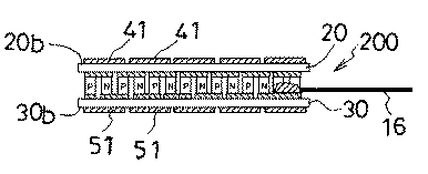
本例における熱電変換装置を図6〜図8に示す。図6は、本例の熱電変換装置200の正面図、図7は本例の熱電変換装置の吸熱側絶縁基板20を他方面20bから見た場合の平面図、図8は本例の熱電変換装置の放熱側絶縁基板30を他方面30bから見た場合の平面図である。本例の熱電変換装置200は、吸熱側絶縁基板20の他方面20bに配設される吸熱側金属板41及び、放熱側絶縁基板30の他方面30bに配設される放熱側金属板51の配設パターンを、5行×5列の計25個の金属板で形成した。また、それぞれの金属板は、同じ形(略正方形)とした。その他の構成は上記第1実施例に記載の熱電変換装置100と同一であるので、具体的な説明は省略する。
The thermoelectric converter in this example is shown in FIGS. 6 is a front view of the thermoelectric conversion device 200 of this example, FIG. 7 is a plan view of the heat absorption
本例に示す熱電変換装置200の信頼性を実証するために、実施例1で説明したのと同様の信頼性評価試験を行った。尚、比較のために、金属板のパターンが4行×4列のもの(図9参照)、3行×3列のもの(図10参照)、2行×2列のもの(図11参照)、分割していない(1行×1列)もの(図12参照)についても、同様の信頼性評価試験を行った。試験結果を表1に示す。
10:熱電変換手段
11、11a、11b:N型熱電素子
12、12a:吸熱側電極
13、13a:P型熱電素子
14,14a:放熱側電極
20:吸熱側絶縁基板、20a:一方面、20b:他方面
30:放熱側絶縁基板、30a:一方面、30b:他方面
41:吸熱側金属板
51:放熱側絶縁板
DESCRIPTION OF SYMBOLS 10: Thermoelectric conversion means 11, 11a, 11b: N type
Claims (3)
一方面に前記複数の吸熱側電極が配設された吸熱側絶縁基板と、
一方面に前記複数の放熱側電極が配設された放熱側絶縁基板とを有する熱電変換装置において、
前記吸熱側絶縁基板及び/又は前記放熱側絶縁基板の他方面には、複数の金属板が各々離間して配設されてなることを特徴とする、熱電変換装置。 A plurality of N-type thermoelectric elements made of an N-type semiconductor material; a plurality of P-type thermoelectric elements made of a P-type semiconductor material; and a plurality of heat radiation side electrodes and heat absorption side electrodes made of a metal material, Thermoelectric conversion means in which the element, the heat absorption side electrode, the P-type thermoelectric element, and the heat radiation side electrode are electrically connected in this order;
A heat-absorbing-side insulating substrate having the plurality of heat-absorbing-side electrodes disposed on one surface;
In the thermoelectric conversion device having a heat radiation side insulating substrate on which one of the plurality of heat radiation side electrodes is disposed,
A thermoelectric conversion device, wherein a plurality of metal plates are disposed separately from each other on the other surface of the heat absorption side insulating substrate and / or the heat radiation side insulating substrate.
前記吸熱側絶縁基板の一方面に配設された前記吸熱側電極の配設パターンは、前記放熱側絶縁基板の他方面に配設された前記金属板の配設パターンと同一であり、
前記放熱側絶縁基板の一方面に配設された前記放熱側電極の配設パターンは、前記吸熱側絶縁基板の他方面に配設された前記金属板の配設パターンと同一であることを特徴とする、熱電変換装置。 In claim 1,
The arrangement pattern of the heat absorption side electrode arranged on one surface of the heat absorption side insulating substrate is the same as the arrangement pattern of the metal plate arranged on the other surface of the heat radiation side insulating substrate,
The disposition pattern of the heat dissipating side electrode disposed on one surface of the heat dissipating side insulating substrate is the same as the disposition pattern of the metal plate disposed on the other surface of the heat absorbing side insulating substrate. A thermoelectric conversion device.
前記各金属板の前記吸熱側絶縁基板及び/又は前記放熱側絶縁基板に対向する面の面積は、全ての金属面の前記吸熱側絶縁基板及び/又は前記放熱側絶縁基板に対向する面の面積の総和の25分の1以下であることを特徴とする、熱電変換装置。 In claim 1,
The area of the surface of each metal plate facing the heat absorption side insulating substrate and / or the heat dissipation side insulating substrate is the area of the surface of all metal surfaces facing the heat absorption side insulating substrate and / or the heat dissipation side insulating substrate. The thermoelectric conversion device is characterized by being less than or equal to 1/25 of the sum of the above.
Priority Applications (1)
| Application Number | Priority Date | Filing Date | Title |
|---|---|---|---|
| JP2003305543A JP4296881B2 (en) | 2003-08-28 | 2003-08-28 | Thermoelectric converter |
Applications Claiming Priority (1)
| Application Number | Priority Date | Filing Date | Title |
|---|---|---|---|
| JP2003305543A JP4296881B2 (en) | 2003-08-28 | 2003-08-28 | Thermoelectric converter |
Publications (2)
| Publication Number | Publication Date |
|---|---|
| JP2005079210A true JP2005079210A (en) | 2005-03-24 |
| JP4296881B2 JP4296881B2 (en) | 2009-07-15 |
Family
ID=34408868
Family Applications (1)
| Application Number | Title | Priority Date | Filing Date |
|---|---|---|---|
| JP2003305543A Expired - Fee Related JP4296881B2 (en) | 2003-08-28 | 2003-08-28 | Thermoelectric converter |
Country Status (1)
| Country | Link |
|---|---|
| JP (1) | JP4296881B2 (en) |
Cited By (23)
| Publication number | Priority date | Publication date | Assignee | Title |
|---|---|---|---|---|
| JP2007266084A (en) * | 2006-03-27 | 2007-10-11 | Yamaha Corp | Thermo module substrate, thermo module, and method of manufacturing thermo module |
| JP2007317865A (en) * | 2006-05-25 | 2007-12-06 | Aisin Seiki Co Ltd | Thermoelectric module |
| WO2008053736A1 (en) * | 2006-10-30 | 2008-05-08 | Kelk Ltd. | Thermoelectric module and metallized substrate |
| JP2008244100A (en) * | 2007-03-27 | 2008-10-09 | Yamaha Corp | Thermoelectric module and method for manufacturing the same |
| US20090025770A1 (en) * | 2007-07-23 | 2009-01-29 | John Lofy | Segmented thermoelectric device |
| JP2009123964A (en) * | 2007-11-15 | 2009-06-04 | Toshiba Corp | Thermoelectric device and thermoelectric module |
| US9335073B2 (en) | 2008-02-01 | 2016-05-10 | Gentherm Incorporated | Climate controlled seating assembly with sensors |
| JP2017069443A (en) * | 2015-09-30 | 2017-04-06 | ヤマハ株式会社 | Thermoelectric conversion module |
| US9622588B2 (en) | 2008-07-18 | 2017-04-18 | Gentherm Incorporated | Environmentally-conditioned bed |
| US9662962B2 (en) | 2013-11-05 | 2017-05-30 | Gentherm Incorporated | Vehicle headliner assembly for zonal comfort |
| US9685599B2 (en) | 2011-10-07 | 2017-06-20 | Gentherm Incorporated | Method and system for controlling an operation of a thermoelectric device |
| US9857107B2 (en) | 2006-10-12 | 2018-01-02 | Gentherm Incorporated | Thermoelectric device with internal sensor |
| US9989267B2 (en) | 2012-02-10 | 2018-06-05 | Gentherm Incorporated | Moisture abatement in heating operation of climate controlled systems |
| US10005337B2 (en) | 2004-12-20 | 2018-06-26 | Gentherm Incorporated | Heating and cooling systems for seating assemblies |
| US10405667B2 (en) | 2007-09-10 | 2019-09-10 | Gentherm Incorporated | Climate controlled beds and methods of operating the same |
| CN112467021A (en) * | 2020-12-04 | 2021-03-09 | 杭州大和热磁电子有限公司 | Thermoelectric module with novel structure and manufacturing method thereof |
| US10991869B2 (en) | 2018-07-30 | 2021-04-27 | Gentherm Incorporated | Thermoelectric device having a plurality of sealing materials |
| US11033058B2 (en) | 2014-11-14 | 2021-06-15 | Gentherm Incorporated | Heating and cooling technologies |
| US11152557B2 (en) | 2019-02-20 | 2021-10-19 | Gentherm Incorporated | Thermoelectric module with integrated printed circuit board |
| US11240882B2 (en) | 2014-02-14 | 2022-02-01 | Gentherm Incorporated | Conductive convective climate controlled seat |
| US11639816B2 (en) | 2014-11-14 | 2023-05-02 | Gentherm Incorporated | Heating and cooling technologies including temperature regulating pad wrap and technologies with liquid system |
| US11857004B2 (en) | 2014-11-14 | 2024-01-02 | Gentherm Incorporated | Heating and cooling technologies |
| US11993132B2 (en) | 2018-11-30 | 2024-05-28 | Gentherm Incorporated | Thermoelectric conditioning system and methods |
-
2003
- 2003-08-28 JP JP2003305543A patent/JP4296881B2/en not_active Expired - Fee Related
Cited By (40)
| Publication number | Priority date | Publication date | Assignee | Title |
|---|---|---|---|---|
| US10005337B2 (en) | 2004-12-20 | 2018-06-26 | Gentherm Incorporated | Heating and cooling systems for seating assemblies |
| JP2007266084A (en) * | 2006-03-27 | 2007-10-11 | Yamaha Corp | Thermo module substrate, thermo module, and method of manufacturing thermo module |
| JP2007317865A (en) * | 2006-05-25 | 2007-12-06 | Aisin Seiki Co Ltd | Thermoelectric module |
| US7893345B2 (en) * | 2006-05-25 | 2011-02-22 | Aisin Seiki Kabushiki Kaisha | Thermoelectric module device |
| US9857107B2 (en) | 2006-10-12 | 2018-01-02 | Gentherm Incorporated | Thermoelectric device with internal sensor |
| WO2008053736A1 (en) * | 2006-10-30 | 2008-05-08 | Kelk Ltd. | Thermoelectric module and metallized substrate |
| JP2008112806A (en) * | 2006-10-30 | 2008-05-15 | Komatsu Electronics Inc | Thermoelectric module and metallized substrate |
| CN101558505B (en) * | 2006-10-30 | 2011-12-21 | Kelk株式会社 | Thermoelectric module and metallized substrate |
| JP2008244100A (en) * | 2007-03-27 | 2008-10-09 | Yamaha Corp | Thermoelectric module and method for manufacturing the same |
| US9105809B2 (en) * | 2007-07-23 | 2015-08-11 | Gentherm Incorporated | Segmented thermoelectric device |
| US20090025770A1 (en) * | 2007-07-23 | 2009-01-29 | John Lofy | Segmented thermoelectric device |
| US10405667B2 (en) | 2007-09-10 | 2019-09-10 | Gentherm Incorporated | Climate controlled beds and methods of operating the same |
| JP2009123964A (en) * | 2007-11-15 | 2009-06-04 | Toshiba Corp | Thermoelectric device and thermoelectric module |
| US10228166B2 (en) | 2008-02-01 | 2019-03-12 | Gentherm Incorporated | Condensation and humidity sensors for thermoelectric devices |
| US9651279B2 (en) | 2008-02-01 | 2017-05-16 | Gentherm Incorporated | Condensation and humidity sensors for thermoelectric devices |
| US9335073B2 (en) | 2008-02-01 | 2016-05-10 | Gentherm Incorporated | Climate controlled seating assembly with sensors |
| US12016466B2 (en) | 2008-07-18 | 2024-06-25 | Sleep Number Corporation | Environmentally-conditioned mattress |
| US12274365B2 (en) | 2008-07-18 | 2025-04-15 | Sleep Number Corporation | Climate controlled bed with fluid distribution member |
| US9622588B2 (en) | 2008-07-18 | 2017-04-18 | Gentherm Incorporated | Environmentally-conditioned bed |
| US10226134B2 (en) | 2008-07-18 | 2019-03-12 | Gentherm Incorporated | Environmentally-conditioned bed |
| US11297953B2 (en) | 2008-07-18 | 2022-04-12 | Sleep Number Corporation | Environmentally-conditioned bed |
| US10208990B2 (en) | 2011-10-07 | 2019-02-19 | Gentherm Incorporated | Thermoelectric device controls and methods |
| US9685599B2 (en) | 2011-10-07 | 2017-06-20 | Gentherm Incorporated | Method and system for controlling an operation of a thermoelectric device |
| US9989267B2 (en) | 2012-02-10 | 2018-06-05 | Gentherm Incorporated | Moisture abatement in heating operation of climate controlled systems |
| US10495322B2 (en) | 2012-02-10 | 2019-12-03 | Gentherm Incorporated | Moisture abatement in heating operation of climate controlled systems |
| US9662962B2 (en) | 2013-11-05 | 2017-05-30 | Gentherm Incorporated | Vehicle headliner assembly for zonal comfort |
| US10266031B2 (en) | 2013-11-05 | 2019-04-23 | Gentherm Incorporated | Vehicle headliner assembly for zonal comfort |
| US11240883B2 (en) | 2014-02-14 | 2022-02-01 | Gentherm Incorporated | Conductive convective climate controlled seat |
| US11240882B2 (en) | 2014-02-14 | 2022-02-01 | Gentherm Incorporated | Conductive convective climate controlled seat |
| US11033058B2 (en) | 2014-11-14 | 2021-06-15 | Gentherm Incorporated | Heating and cooling technologies |
| US11857004B2 (en) | 2014-11-14 | 2024-01-02 | Gentherm Incorporated | Heating and cooling technologies |
| US11639816B2 (en) | 2014-11-14 | 2023-05-02 | Gentherm Incorporated | Heating and cooling technologies including temperature regulating pad wrap and technologies with liquid system |
| JP2017069443A (en) * | 2015-09-30 | 2017-04-06 | ヤマハ株式会社 | Thermoelectric conversion module |
| US11223004B2 (en) | 2018-07-30 | 2022-01-11 | Gentherm Incorporated | Thermoelectric device having a polymeric coating |
| US11075331B2 (en) | 2018-07-30 | 2021-07-27 | Gentherm Incorporated | Thermoelectric device having circuitry with structural rigidity |
| US10991869B2 (en) | 2018-07-30 | 2021-04-27 | Gentherm Incorporated | Thermoelectric device having a plurality of sealing materials |
| US11993132B2 (en) | 2018-11-30 | 2024-05-28 | Gentherm Incorporated | Thermoelectric conditioning system and methods |
| US12459335B2 (en) | 2018-11-30 | 2025-11-04 | Gentherm Incorporated | Thermoelectric conditioning system and methods |
| US11152557B2 (en) | 2019-02-20 | 2021-10-19 | Gentherm Incorporated | Thermoelectric module with integrated printed circuit board |
| CN112467021A (en) * | 2020-12-04 | 2021-03-09 | 杭州大和热磁电子有限公司 | Thermoelectric module with novel structure and manufacturing method thereof |
Also Published As
| Publication number | Publication date |
|---|---|
| JP4296881B2 (en) | 2009-07-15 |
Similar Documents
| Publication | Publication Date | Title |
|---|---|---|
| JP4296881B2 (en) | Thermoelectric converter | |
| KR101554647B1 (en) | Circuit assemblies including thermoelectric modules | |
| JP4768961B2 (en) | Thermoelectric module having thin film substrate | |
| US7795711B2 (en) | Microelectronic cooling apparatus and associated method | |
| JP5956608B2 (en) | Thermoelectric module | |
| US9516790B2 (en) | Thermoelectric cooler/heater integrated in printed circuit board | |
| KR20070034006A (en) | Thermoelectric module | |
| JP2000058930A (en) | Thermoelement, and its manufacture | |
| JP2008277584A (en) | Thermoelectric substrate member, thermoelectric module, and manufacturing method thereof | |
| TWI514528B (en) | Semiconductor wafer structure | |
| JP4663469B2 (en) | Heat exchanger | |
| US20120060889A1 (en) | Thermoelectric modules and assemblies with stress reducing structure | |
| KR20150146365A (en) | Substrate having an thermoelectric module and semiconductor package using the same | |
| JP2017041620A (en) | Thermoelectric converter and thermoelectric conversion system | |
| JP2007035907A (en) | Thermoelectric module | |
| KR20090120437A (en) | Thermoelectric module with heat transfer member | |
| JP5865721B2 (en) | Thermoelectric module | |
| JP2006216642A (en) | Thermoelectric element | |
| JP4737436B2 (en) | Thermoelectric conversion module assembly | |
| JP2011082272A (en) | Thermoelectric cooling device | |
| JP6592996B2 (en) | Thermoelectric generator | |
| JP3007904U (en) | Thermal battery | |
| JP2005174985A (en) | Thermoelectric element | |
| JP2005057124A (en) | Module and device for thermoelectric conversion | |
| JP2005109141A (en) | Thermoelectric module and thermoelectric module application equipment |
Legal Events
| Date | Code | Title | Description |
|---|---|---|---|
| A621 | Written request for application examination |
Free format text: JAPANESE INTERMEDIATE CODE: A621 Effective date: 20060727 |
|
| A977 | Report on retrieval |
Free format text: JAPANESE INTERMEDIATE CODE: A971007 Effective date: 20090108 |
|
| A131 | Notification of reasons for refusal |
Free format text: JAPANESE INTERMEDIATE CODE: A131 Effective date: 20090113 |
|
| A521 | Request for written amendment filed |
Free format text: JAPANESE INTERMEDIATE CODE: A523 Effective date: 20090227 |
|
| TRDD | Decision of grant or rejection written | ||
| A01 | Written decision to grant a patent or to grant a registration (utility model) |
Free format text: JAPANESE INTERMEDIATE CODE: A01 Effective date: 20090324 |
|
| A01 | Written decision to grant a patent or to grant a registration (utility model) |
Free format text: JAPANESE INTERMEDIATE CODE: A01 |
|
| A61 | First payment of annual fees (during grant procedure) |
Free format text: JAPANESE INTERMEDIATE CODE: A61 Effective date: 20090406 |
|
| FPAY | Renewal fee payment (event date is renewal date of database) |
Free format text: PAYMENT UNTIL: 20120424 Year of fee payment: 3 |
|
| FPAY | Renewal fee payment (event date is renewal date of database) |
Free format text: PAYMENT UNTIL: 20120424 Year of fee payment: 3 |
|
| FPAY | Renewal fee payment (event date is renewal date of database) |
Free format text: PAYMENT UNTIL: 20130424 Year of fee payment: 4 |
|
| FPAY | Renewal fee payment (event date is renewal date of database) |
Free format text: PAYMENT UNTIL: 20130424 Year of fee payment: 4 |
|
| FPAY | Renewal fee payment (event date is renewal date of database) |
Free format text: PAYMENT UNTIL: 20140424 Year of fee payment: 5 |
|
| LAPS | Cancellation because of no payment of annual fees |