JP2005062724A - Optical phase difference plate and liquid crystal display - Google Patents
Optical phase difference plate and liquid crystal display Download PDFInfo
- Publication number
- JP2005062724A JP2005062724A JP2003296003A JP2003296003A JP2005062724A JP 2005062724 A JP2005062724 A JP 2005062724A JP 2003296003 A JP2003296003 A JP 2003296003A JP 2003296003 A JP2003296003 A JP 2003296003A JP 2005062724 A JP2005062724 A JP 2005062724A
- Authority
- JP
- Japan
- Prior art keywords
- liquid crystal
- display device
- crystal display
- phase difference
- optical
- Prior art date
- Legal status (The legal status is an assumption and is not a legal conclusion. Google has not performed a legal analysis and makes no representation as to the accuracy of the status listed.)
- Pending
Links
Images


Classifications
-
- G—PHYSICS
- G02—OPTICS
- G02F—OPTICAL DEVICES OR ARRANGEMENTS FOR THE CONTROL OF LIGHT BY MODIFICATION OF THE OPTICAL PROPERTIES OF THE MEDIA OF THE ELEMENTS INVOLVED THEREIN; NON-LINEAR OPTICS; FREQUENCY-CHANGING OF LIGHT; OPTICAL LOGIC ELEMENTS; OPTICAL ANALOGUE/DIGITAL CONVERTERS
- G02F1/00—Devices or arrangements for the control of the intensity, colour, phase, polarisation or direction of light arriving from an independent light source, e.g. switching, gating or modulating; Non-linear optics
- G02F1/01—Devices or arrangements for the control of the intensity, colour, phase, polarisation or direction of light arriving from an independent light source, e.g. switching, gating or modulating; Non-linear optics for the control of the intensity, phase, polarisation or colour
- G02F1/13—Devices or arrangements for the control of the intensity, colour, phase, polarisation or direction of light arriving from an independent light source, e.g. switching, gating or modulating; Non-linear optics for the control of the intensity, phase, polarisation or colour based on liquid crystals, e.g. single liquid crystal display cells
- G02F1/133—Constructional arrangements; Operation of liquid crystal cells; Circuit arrangements
- G02F1/1333—Constructional arrangements; Manufacturing methods
- G02F1/1335—Structural association of cells with optical devices, e.g. polarisers or reflectors
- G02F1/13363—Birefringent elements, e.g. for optical compensation
- G02F1/133632—Birefringent elements, e.g. for optical compensation with refractive index ellipsoid inclined relative to the LC-layer surface
-
- G—PHYSICS
- G02—OPTICS
- G02F—OPTICAL DEVICES OR ARRANGEMENTS FOR THE CONTROL OF LIGHT BY MODIFICATION OF THE OPTICAL PROPERTIES OF THE MEDIA OF THE ELEMENTS INVOLVED THEREIN; NON-LINEAR OPTICS; FREQUENCY-CHANGING OF LIGHT; OPTICAL LOGIC ELEMENTS; OPTICAL ANALOGUE/DIGITAL CONVERTERS
- G02F1/00—Devices or arrangements for the control of the intensity, colour, phase, polarisation or direction of light arriving from an independent light source, e.g. switching, gating or modulating; Non-linear optics
- G02F1/01—Devices or arrangements for the control of the intensity, colour, phase, polarisation or direction of light arriving from an independent light source, e.g. switching, gating or modulating; Non-linear optics for the control of the intensity, phase, polarisation or colour
- G02F1/13—Devices or arrangements for the control of the intensity, colour, phase, polarisation or direction of light arriving from an independent light source, e.g. switching, gating or modulating; Non-linear optics for the control of the intensity, phase, polarisation or colour based on liquid crystals, e.g. single liquid crystal display cells
- G02F1/133—Constructional arrangements; Operation of liquid crystal cells; Circuit arrangements
- G02F1/1333—Constructional arrangements; Manufacturing methods
- G02F1/1335—Structural association of cells with optical devices, e.g. polarisers or reflectors
- G02F1/13363—Birefringent elements, e.g. for optical compensation
-
- G—PHYSICS
- G02—OPTICS
- G02F—OPTICAL DEVICES OR ARRANGEMENTS FOR THE CONTROL OF LIGHT BY MODIFICATION OF THE OPTICAL PROPERTIES OF THE MEDIA OF THE ELEMENTS INVOLVED THEREIN; NON-LINEAR OPTICS; FREQUENCY-CHANGING OF LIGHT; OPTICAL LOGIC ELEMENTS; OPTICAL ANALOGUE/DIGITAL CONVERTERS
- G02F1/00—Devices or arrangements for the control of the intensity, colour, phase, polarisation or direction of light arriving from an independent light source, e.g. switching, gating or modulating; Non-linear optics
- G02F1/01—Devices or arrangements for the control of the intensity, colour, phase, polarisation or direction of light arriving from an independent light source, e.g. switching, gating or modulating; Non-linear optics for the control of the intensity, phase, polarisation or colour
- G02F1/13—Devices or arrangements for the control of the intensity, colour, phase, polarisation or direction of light arriving from an independent light source, e.g. switching, gating or modulating; Non-linear optics for the control of the intensity, phase, polarisation or colour based on liquid crystals, e.g. single liquid crystal display cells
- G02F1/133—Constructional arrangements; Operation of liquid crystal cells; Circuit arrangements
- G02F1/136—Liquid crystal cells structurally associated with a semi-conducting layer or substrate, e.g. cells forming part of an integrated circuit
- G02F1/1362—Active matrix addressed cells
- G02F1/136222—Colour filters incorporated in the active matrix substrate
-
- G—PHYSICS
- G02—OPTICS
- G02F—OPTICAL DEVICES OR ARRANGEMENTS FOR THE CONTROL OF LIGHT BY MODIFICATION OF THE OPTICAL PROPERTIES OF THE MEDIA OF THE ELEMENTS INVOLVED THEREIN; NON-LINEAR OPTICS; FREQUENCY-CHANGING OF LIGHT; OPTICAL LOGIC ELEMENTS; OPTICAL ANALOGUE/DIGITAL CONVERTERS
- G02F1/00—Devices or arrangements for the control of the intensity, colour, phase, polarisation or direction of light arriving from an independent light source, e.g. switching, gating or modulating; Non-linear optics
- G02F1/01—Devices or arrangements for the control of the intensity, colour, phase, polarisation or direction of light arriving from an independent light source, e.g. switching, gating or modulating; Non-linear optics for the control of the intensity, phase, polarisation or colour
- G02F1/13—Devices or arrangements for the control of the intensity, colour, phase, polarisation or direction of light arriving from an independent light source, e.g. switching, gating or modulating; Non-linear optics for the control of the intensity, phase, polarisation or colour based on liquid crystals, e.g. single liquid crystal display cells
- G02F1/137—Devices or arrangements for the control of the intensity, colour, phase, polarisation or direction of light arriving from an independent light source, e.g. switching, gating or modulating; Non-linear optics for the control of the intensity, phase, polarisation or colour based on liquid crystals, e.g. single liquid crystal display cells characterised by the electro-optical or magneto-optical effect, e.g. field-induced phase transition, orientation effect, guest-host interaction or dynamic scattering
- G02F1/139—Devices or arrangements for the control of the intensity, colour, phase, polarisation or direction of light arriving from an independent light source, e.g. switching, gating or modulating; Non-linear optics for the control of the intensity, phase, polarisation or colour based on liquid crystals, e.g. single liquid crystal display cells characterised by the electro-optical or magneto-optical effect, e.g. field-induced phase transition, orientation effect, guest-host interaction or dynamic scattering based on orientation effects in which the liquid crystal remains transparent
- G02F1/1393—Devices or arrangements for the control of the intensity, colour, phase, polarisation or direction of light arriving from an independent light source, e.g. switching, gating or modulating; Non-linear optics for the control of the intensity, phase, polarisation or colour based on liquid crystals, e.g. single liquid crystal display cells characterised by the electro-optical or magneto-optical effect, e.g. field-induced phase transition, orientation effect, guest-host interaction or dynamic scattering based on orientation effects in which the liquid crystal remains transparent the birefringence of the liquid crystal being electrically controlled, e.g. ECB-, DAP-, HAN-, PI-LC cells
-
- G—PHYSICS
- G02—OPTICS
- G02F—OPTICAL DEVICES OR ARRANGEMENTS FOR THE CONTROL OF LIGHT BY MODIFICATION OF THE OPTICAL PROPERTIES OF THE MEDIA OF THE ELEMENTS INVOLVED THEREIN; NON-LINEAR OPTICS; FREQUENCY-CHANGING OF LIGHT; OPTICAL LOGIC ELEMENTS; OPTICAL ANALOGUE/DIGITAL CONVERTERS
- G02F2413/00—Indexing scheme related to G02F1/13363, i.e. to birefringent elements, e.g. for optical compensation, characterised by the number, position, orientation or value of the compensation plates
- G02F2413/10—Indexing scheme related to G02F1/13363, i.e. to birefringent elements, e.g. for optical compensation, characterised by the number, position, orientation or value of the compensation plates with refractive index ellipsoid inclined, or tilted, relative to the LC-layer surface O plate
- G02F2413/105—Indexing scheme related to G02F1/13363, i.e. to birefringent elements, e.g. for optical compensation, characterised by the number, position, orientation or value of the compensation plates with refractive index ellipsoid inclined, or tilted, relative to the LC-layer surface O plate with varying inclination in thickness direction, e.g. hybrid oriented discotic LC
Landscapes
- Physics & Mathematics (AREA)
- Nonlinear Science (AREA)
- Mathematical Physics (AREA)
- Chemical & Material Sciences (AREA)
- Crystallography & Structural Chemistry (AREA)
- General Physics & Mathematics (AREA)
- Optics & Photonics (AREA)
- Liquid Crystal (AREA)
- Polarising Elements (AREA)
Abstract
Description
本発明は、液晶分子が黒表示のために例えば略垂直に配向される液晶パネルに適用される光学位相差板およびこの光学位相差板を用いる液晶表示装置に関する。 The present invention relates to an optical retardation plate applied to a liquid crystal panel in which liquid crystal molecules are aligned substantially vertically for black display and a liquid crystal display device using the optical retardation plate.
液晶表示装置は軽量、薄型、低消費電力という特徴を有し、この特徴からOA機器、情報端末、時計、テレビのような様々な分野で応用されている。特にアクティブマトリクス型液晶表示装置は、薄膜トランジスタ(Thin Film Transistor)を用いて画素のスイッチングを行うことにより優れた応答性を得ることができる液晶表示装置であるため、多くの画像情報を表示しなくてはならない携帯テレビあるいはコンピュータの表示モニタとして利用されている。 A liquid crystal display device has features such as light weight, thinness, and low power consumption, and is applied in various fields such as OA equipment, information terminals, watches, and televisions. In particular, an active matrix liquid crystal display device is a liquid crystal display device that can obtain excellent responsiveness by switching pixels using thin film transistors, so that it does not display much image information. It is used as a display monitor for portable TVs or computers that should not be used.
近年では、液晶表示装置の精細度および表示速度の向上が情報量の増大に伴って要求され始めている。高精細化は、例えば薄膜トランジスタのアレイ構造を微細化して画素数を増大することにより実現されている。 In recent years, improvements in the definition and display speed of liquid crystal display devices have begun to be demanded as the amount of information increases. High definition is realized, for example, by miniaturizing the array structure of thin film transistors to increase the number of pixels.
一方、表示速度の高速化に関しては、従来の表示モードに代わって、例えばネマティック液晶を用いたOCB(Optically Compensated Birefringence)モード、VAN(Vertically Aligned Nematic)モード、HAN(Hybrid Aligned Nematic)モード、およびπ配列モード、並びにスメクチック液晶を用いた界面安定型強誘電性液晶(SSFLC: Surface-Stabilized Ferroelectric Liquid Crystal)モードおよび反強誘電性液晶(AFLC: Anti-Ferroelectric Liquid Crystal)モードが検討されている。 On the other hand, regarding the increase in display speed, instead of the conventional display mode, for example, OCB (Optically Compensated Birefringence) mode using nematic liquid crystal, VAN (Vertically Aligned Nematic) mode, HAN (Hybrid Aligned Nematic) mode, and π An arrangement mode, and an interface-stable ferroelectric liquid crystal (SSFLC) mode and an anti-ferroelectric liquid crystal (AFLC) mode using a smectic liquid crystal have been studied.
これら表示モードのうち、特にVANモードは従来のツイストネマチック(Twisted Nematic)モードよりも速い応答速度を得ることができ、さらに静電気破壊のような不良発生の原因となるラビング処理を垂直配向により不要にできるという特長を有する。なかでも、マルチドメイン型VANモード(以下、MVAモードという)は視野角の拡大が比較的容易なことから特に注目されている。 Among these display modes, the VAN mode, in particular, can obtain a faster response speed than the conventional Twisted Nematic mode, and further eliminates rubbing that causes defects such as electrostatic breakdown by vertical alignment. It has the feature that it can. Among them, the multi-domain VAN mode (hereinafter referred to as MVA mode) is particularly attracting attention because it is relatively easy to expand the viewing angle.
マルチドメイン構造を得る方式としては、アレイ基板上の画素電極および対向基板上の対向電極に配向分割用の電極スリットや突起を設け、これらによって画素電極および対向電極から画素領域に印加される電界の傾きを制御することが一般的に行われている(例えば特許文献1参照)。この場合、液晶層の画素領域は液晶分子の配向方向が電圧印加状態で互いに90°の角度をなすような例えば4つのドメインに配向分割され、これにより視角特性の対称性改善と反転現象の抑止を実現している。また、負の光学位相差板が、電極基板に対して垂直に液晶分子を配列させる黒表示状態で液晶層に生じる位相差の視角依存性を補償するために用いられ、これにより視角に対するコントラスト(CR)を良好なものとしている。この負の光学位相差板が偏光板の視角依存性も補償するような面内位相差を持つ2軸位相差板であれば、さらに優れた視角−コントラスト特性を実現することができる。
しかしながら、上述したMVAモードでは、視角補償が黒表示(最小)階調以外で不十分であり、輝度(透過率)特性がパネル正面の方位と斜めの方位との間で異なる。液晶表示装置が画素領域を4つのドメインに配向分割するMVAモードである場合、例えば図24〜図26に示すようなパネル正面の方位を0°とした視角−輝度特性が様々な階調に対応する液晶印加電圧の下で得られる。図24はパネル正面の方位に対して左右方位において得られる視角−輝度特性を示し、図25はパネル正面の方位に対して斜め方位において得られる視角−輝度特性を示し、図26はパネル正面の方位に対して上下方位において得られる視角−輝度特性を示す。ここでは、0Vから4.7Vの範囲の電圧が液晶層LQに印加された。図24〜図26では、横軸がパネル正面の方位を0°とした視角を示し、縦軸がパネルの輝度を透過率で示す。これらの視角輝度特性によれば、中間階調での輝度差がパネル正面に対して斜めの方位となる視角において縮小し、さらに白表示(最大)階調での輝度も視角依存性によって低下することから、多色表示であるときに全体的に白茶けて見えるという問題を有することがわかる。 However, in the MVA mode described above, the viewing angle compensation is insufficient except for the black display (minimum) gradation, and the luminance (transmittance) characteristics differ between the front direction of the panel and the oblique direction. When the liquid crystal display device is in the MVA mode in which the pixel region is aligned and divided into four domains, the viewing angle-luminance characteristics with the panel front direction being 0 ° as shown in FIGS. Is obtained under a liquid crystal applied voltage. 24 shows viewing angle-luminance characteristics obtained in the left-right direction with respect to the front direction of the panel, FIG. 25 shows viewing angle-luminance characteristics obtained in the oblique direction with respect to the direction of the panel front, and FIG. The viewing angle-luminance characteristics obtained in the vertical direction with respect to the direction are shown. Here, a voltage in the range of 0 V to 4.7 V was applied to the liquid crystal layer LQ. 24 to 26, the horizontal axis represents the viewing angle with the orientation of the front of the panel being 0 °, and the vertical axis represents the panel luminance in terms of transmittance. According to these viewing angle luminance characteristics, the luminance difference at the intermediate gradation is reduced at the viewing angle that is oblique to the front of the panel, and the luminance at the white display (maximum) gradation is also reduced due to the viewing angle dependency. From this, it can be seen that there is a problem that the image appears to be totally brown when multi-color display is performed.
また、上述したMVAモードにおいて4つのドメインを得るために設置される突起や電極スリット、並びにこれらドメイン間の配向境界に発生するシュリーレン配向の影響により、液晶表示装置の輝度が配向分割を行わない場合よりも著しく劣化するという問題も生じている。この問題を改善するために配向分割数を少なくすることも考えられるが、次のような理由から難しい。すなわち、画素領域の配向分割数が4である場合、液晶表示装置は図30に示すような視角−コントラスト特性を有する。この視角−コントラスト特性はコントラスト(CR)が全方位において10以上である点で優れている。 In addition, when the luminance of the liquid crystal display device does not perform alignment division due to the influence of the schlieren alignment generated at the alignment boundary between the projections and electrode slits installed in these MVA modes and the alignment boundary between these domains. There is also a problem that it is significantly deteriorated. Although it is conceivable to reduce the number of alignment divisions in order to improve this problem, it is difficult for the following reasons. That is, when the number of alignment divisions in the pixel region is 4, the liquid crystal display device has viewing angle-contrast characteristics as shown in FIG. This viewing angle-contrast characteristic is excellent in that the contrast (CR) is 10 or more in all directions.
また、画素領域の配向分割数が2である場合、液晶表示装置は図27〜図29に示すような視角−コントラスト特性を有する。この視角−コントラスト特性は、配向分割数が4である液晶表示装置のそれと同等である。しかしながら、この液晶表示装置は図27〜図29に示すような視角−輝度特性を有する。これらの図によれば、輝度反転が中間階調において生じることがわかる。中間階調における位相差の異方性は液晶分子の配向方向が2つのドメイン間で反平行となる上下方位で補償しあうが、左右方位で一様に作用する。すなわち、輝度反転は印加電圧に対する位相差の変化度がパネル正面と視角方位との間で変わるために生じる。従って、配向分割数が2の場合、液晶表示装置の輝度は改善されるが、視角−輝度特性は中間階調で劣ってしまうという問題が生じる。 When the number of alignment divisions in the pixel region is 2, the liquid crystal display device has viewing angle-contrast characteristics as shown in FIGS. This viewing angle-contrast characteristic is equivalent to that of a liquid crystal display device having four alignment divisions. However, this liquid crystal display device has viewing angle-luminance characteristics as shown in FIGS. According to these figures, it can be seen that the luminance inversion occurs in the intermediate gradation. The anisotropy of the phase difference in the intermediate gradation is compensated by the vertical direction in which the alignment direction of the liquid crystal molecules is antiparallel between the two domains, but acts uniformly in the horizontal direction. That is, luminance inversion occurs because the degree of change in phase difference with respect to the applied voltage changes between the front of the panel and the viewing angle azimuth. Therefore, when the number of alignment divisions is 2, the luminance of the liquid crystal display device is improved, but there is a problem that the viewing angle-luminance characteristics are inferior in the intermediate gradation.
本発明は、上記問題点に鑑みてなされたものであり、液晶層の液晶分子を黒表示用の垂直配列状態と白表示用の水平配列状態またはハイブリッド配列状態との間で遷移させる電界により液晶層の位相差および旋光性を制御する液晶表示モードにおいて視角−コントラスト特性を損なうことなく中間階調での視角−輝度特性を向上させることが可能な光学位相差板および液晶表示装置を提供することにある。 The present invention has been made in view of the above problems, and a liquid crystal is produced by an electric field that causes liquid crystal molecules in a liquid crystal layer to transition between a vertical alignment state for black display and a horizontal alignment state or a hybrid alignment state for white display. To provide an optical phase difference plate and a liquid crystal display device capable of improving the viewing angle-luminance characteristics at intermediate gradation without impairing the viewing angle-contrast characteristics in the liquid crystal display mode for controlling the phase difference and optical rotation of the layers. It is in.
本発明によれば、円盤状の高分子からなり厚さ方向に直角な平面に対して徐々に傾斜して厚さ方向にハイブリッド配列される一群の屈折率楕円体をそれぞれ含む少なくとも一対の第1および第2光学フィルムを備え、屈折率楕円体の傾斜方位は第1光学フィルムおよび第2光学フィルム間で互いに反平行な関係にある光学位相差板が提供される。 According to the present invention, at least a pair of first ellipsoids each including a group of refractive index ellipsoids made of a disk-shaped polymer and gradually inclined with respect to a plane perpendicular to the thickness direction and hybrid-arranged in the thickness direction. And an optical phase difference plate having a refractive index ellipsoid having an antiparallel relationship between the first optical film and the second optical film.
さらに本発明によれば、液晶層が一対の電極基板間に挟持される構造の液晶パネルと、液晶パネルを挟持する一対の偏光板と、液晶パネルと一対の偏光板間に配置される一対の光学位相差板とを備え、各光学位相差板は互いに直交するx軸方向およびy軸方向、z軸方向の平均屈折率nx,ny,nzがz軸方向を法線方向に一致させた状態でnx>ny>nzの関係にある屈折率異方性を有し、各光学位相差板のx軸方向とこの光学位相差板に隣接する偏光板の透過軸とは略平行である液晶表示装置が提供される。 Furthermore, according to the present invention, a liquid crystal panel having a structure in which a liquid crystal layer is sandwiched between a pair of electrode substrates, a pair of polarizing plates that sandwich the liquid crystal panel, and a pair of liquid crystal panels disposed between the pair of polarizing plates. Each optical phase difference plate is in a state in which the average refractive indexes nx, ny, and nz in the x-axis direction, the y-axis direction, and the z-axis direction that are orthogonal to each other coincide with the normal direction. A liquid crystal display having refractive index anisotropy in a relationship of nx> ny> nz, and the x-axis direction of each optical phase difference plate and the transmission axis of a polarizing plate adjacent to the optical phase difference plate being substantially parallel An apparatus is provided.
これら光学位相差板および液晶表示装置では、光学位相差板が配列遷移中において全ての液晶分子の配列状態に対して液晶層の位相差の視角依存性および偏光板の視角依存性を補償することができる。従って、視角−コントラスト特性を損なうことなく中間階調での視角−輝度特性を向上させることが可能である。特に、液晶層がMVAモードのように配向分割される場合において、配向分割数が2分割であっても、視角−コントラスト特性を損なうことなく中間階調での視角−輝度特性を向上させることが可能である。 In these optical phase difference plates and liquid crystal display devices, the optical phase difference plate compensates for the viewing angle dependency of the retardation of the liquid crystal layer and the viewing angle dependency of the polarizing plate with respect to the alignment state of all liquid crystal molecules during the alignment transition. Can do. Therefore, it is possible to improve the viewing angle-luminance characteristics in the intermediate gradation without impairing the viewing angle-contrast characteristics. In particular, when the liquid crystal layer is aligned and divided as in the MVA mode, even if the number of alignment divisions is 2, the viewing angle-luminance characteristics in the intermediate gradation can be improved without impairing the viewing angle-contrast characteristics. Is possible.
本発明によれば、液晶層の液晶分子を黒表示用の垂直配列状態と白表示用の水平配列状態またはハイブリッド配列状態との間で遷移させる電界により液晶層の位相差および旋光性を制御する液晶表示モードにおいて視角−コントラスト特性を損なうことなく中間階調での視角−輝度特性を向上させることが可能な光学位相差板および液晶表示装置を提供することができる。 According to the present invention, the phase difference and optical rotation of the liquid crystal layer are controlled by an electric field that causes liquid crystal molecules in the liquid crystal layer to transition between a vertical alignment state for black display and a horizontal alignment state for white display or a hybrid alignment state. It is possible to provide an optical phase difference plate and a liquid crystal display device capable of improving the viewing angle-luminance characteristics in the intermediate gradation without impairing the viewing angle-contrast characteristics in the liquid crystal display mode.
以下、本発明の第1実施形態に係る液晶表示装置について添付図面を参照して説明する。この液晶表示装置はMVAモードで表示を行う透過型液晶表示装置である。 Hereinafter, a liquid crystal display device according to a first embodiment of the present invention will be described with reference to the accompanying drawings. This liquid crystal display device is a transmissive liquid crystal display device that performs display in the MVA mode.
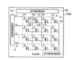
図1はこの液晶表示装置TMDの外観を示し、図2は図1に示す液晶表示装置TMDの回路構造を概略的に示し、図3は図1に示す液晶表示装置TMDの断面構造を示す。 FIG. 1 shows an appearance of the liquid crystal display device TMD, FIG. 2 schematically shows a circuit structure of the liquid crystal display device TMD shown in FIG. 1, and FIG. 3 shows a cross-sectional structure of the liquid crystal display device TMD shown in FIG.
図1に示すように、液晶表示装置TMDは第1電極基板となるアレイ基板ARと、第1電極基板に対向する第2電極基板となる対向基板CTと、負の誘電率異方性を有するネマティック液晶材料を含みアレイ基板ARおよび対向基板CT間に挟持される液晶層LQと、アレイ基板AR,対向基板CT,および液晶層LQからなる液晶パネルDPを挟持する第1および第2偏光板PLと、液晶パネルDPおよび第1偏光板PL間および液晶パネルDPおよび第2偏光板PL間にそれぞれ配置される第1および第2光学位相差板RTとを備える。アレイ基板ARと対向基板CTとは液晶層LQを取り囲むように配置される外縁シール部材11により貼り合わされる。液晶表示装置TMDでは、画像を表示するための表示領域DAが外縁シール部材11の内側に配置され、駆動回路を配置するための周辺領域EAがこの表示領域DAの周囲に配置される。液晶材料はアレイ基板ARと対向基板CTとの貼合わせ後に液晶注入口12から注入され、この注入後に封止部材13により封止される。
As shown in FIG. 1, the liquid crystal display device TMD has an array substrate AR serving as a first electrode substrate, a counter substrate CT serving as a second electrode substrate facing the first electrode substrate, and a negative dielectric anisotropy. A liquid crystal layer LQ that includes a nematic liquid crystal material and is sandwiched between the array substrate AR and the counter substrate CT, and a first and second polarizing plates PL that sandwich a liquid crystal panel DP that includes the array substrate AR, the counter substrate CT, and the liquid crystal layer LQ. And first and second optical retardation plates RT disposed between the liquid crystal panel DP and the first polarizing plate PL and between the liquid crystal panel DP and the second polarizing plate PL, respectively. The array substrate AR and the counter substrate CT are bonded together by an outer
アレイ基板ARは、表示領域DAにおいて、図2に示すように、マトリクス状に配置されたm×n個の画素電極PE、これら画素電極PEの行に沿って配置されたm本の走査線Y(Y1〜Ym)、これら画素電極PEの列方向に沿って配置されたn本の信号線X(X1〜Xn)、m×n個の画素電極PEに対応して走査線Y1〜Ymおよび信号線X1〜Xnの交差位置近傍に配置されたm×n個の画素スイッチ15を有し、さらに画素電極PEの行に沿って配置されるm本の補助容量線16を有する。走査線Y1〜Ymは信号線X1〜Xnと略直交し、補助容量線16と略平行に配置される。各補助容量線16は対向電極駆動回路等から対向電位VCOMとして得られる所定電位に設定され、対応行の画素電極PEと容量結合してそれぞれ補助容量Csを構成する。
As shown in FIG. 2, the array substrate AR includes m × n pixel electrodes PE arranged in a matrix and m scanning lines Y arranged along the rows of the pixel electrodes PE in the display area DA. (Y1 to Ym), n signal lines X (X1 to Xn) arranged along the column direction of the pixel electrodes PE, scanning lines Y1 to Ym and signals corresponding to m × n pixel electrodes PE. It has m ×
また、アレイ基板ARは、周辺領域EAにおいて、走査線Y1〜Ymを駆動する走査線駆動回路YD、信号線X1〜Xnを駆動する信号線駆動回路XDを有する。各画素スイッチ15は例えばポリシリコン薄膜トランジスタからなり、対応走査線Yおよび対応信号線Xに接続され、この走査線Yからの駆動電圧により導通し、信号線Xからの信号電圧を対応画素電極PEに印加する。尚、各画素スイッチ15は、ポリシリコン薄膜トランジスタ以外に、アモルファスシリコン薄膜トランジスタで構成することもできる。
In addition, the array substrate AR has a scanning line driving circuit YD for driving the scanning lines Y1 to Ym and a signal line driving circuit XD for driving the signal lines X1 to Xn in the peripheral area EA. Each
画素電極PEは金属等の遮光性導電部材からなる信号線Xおよび走査線Yによって区画され、電気的に絶縁された状態でこれら信号線Xおよび走査線Yに僅かに重なる。画素電極PEはガラス基板などの光透過性絶縁基板GL上に形成されるITO等の透明導電部材からなり、その平面的な広がりによって液晶層LQの画素領域に電界を形成する。 The pixel electrode PE is partitioned by a signal line X and a scanning line Y made of a light-shielding conductive member such as metal, and slightly overlaps the signal line X and the scanning line Y in an electrically insulated state. The pixel electrode PE is made of a transparent conductive member such as ITO formed on a light transmissive insulating substrate GL such as a glass substrate, and forms an electric field in the pixel region of the liquid crystal layer LQ by its planar spread.
図3に示すように、アレイ基板ARでは、それぞれの画素スイッチ15が光透過性絶縁基板GL上に形成され、カラーフィルタCFにより覆われる。カラーフィルタCFは、複数の画素電極PEの列毎に繰り返し並べられ各々複数の画素電極PEの1つに対向する赤カラーフィルタ層R、緑カラーフィルタ層G、青カラーフィルタ層Bにより構成される。また、複数の柱状スペーサ17がこれら画素電極PE相互間においてカラーフィルタCF上に形成される。カラーフィルタCF、画素電極PE、および柱状スペーサ17は配向膜18により全体的に覆われる。配向膜18は例えばポリイミドなどの透明樹脂からなり、ラビング処理は施さずに垂直配向性を付与されている。配向膜18は、電圧無印加状態において液晶層LQの液晶材料に含まれる液晶分子20をアレイ基板ARに対して略垂直な方向に配向させる。
As shown in FIG. 3, in the array substrate AR, each
画素スイッチ15は絶縁基板GL上のポリシリコン半導体層21にゲート絶縁膜22を介して重なるゲート電極15G、半導体層21においてゲート電極15Gの下方に配置されるチャネル領域21C、不純物のドープにより半導体層21においてチャネル領域21Cの両側に配置されるドレイン領域21Dおよびソース領域21S、ドレイン領域21Dに接続されるドレイン電極15D、並びにソース領域21Sに接続されるソース電極15Sを有する。信号線X、走査線Y、および補助容量線16等の配線部、画素スイッチ15のゲート電極15G、ドレイン電極15D、およびソース電極15Sは、アルミニウム、モリブデン、銅、タンタルなどの遮光性導電部材を用いて形成される。具体的には、走査線Y、補助容量線16、およびゲート電極15Gは、ゲート絶縁膜22を覆う導電層をパターニングすることによりそれぞれ形成される。本実施形態において、ゲート電極15Gは走査線Yの一部となっている。
The
信号線X、ドレイン電極15D、およびソース電極15Sは、走査線Y、補助容量線16、ゲート電極15G、およびゲート絶縁膜22を覆う層間絶縁膜23上に形成される導電層をパターニングすることによりそれぞれ形成される。ここで、ドレイン電極15Dはゲート絶縁膜22および層間絶縁膜23を貫通するコンタクトホール内でドレイン領域21Dにコンタクトして信号線Xと一体的に形成され、ソース電極15Sはゲート絶縁膜22および層間絶縁膜23を貫通するコンタクトホール内でソース領域21Sにコンタクトして形成される。ソース領域21Sはゲート絶縁膜22を介して補助容量線16と対向する。カラーフィルタCFは信号線X、ドレイン電極15D、およびソース電極15Sを覆って形成される。画素電極PEは、カラーフィルタCFを貫通するコンタクトホール24内で画素スイッチ15のソース電極15Sにコンタクトするように形成される。ソース領域21Sおよび画素電極PEは補助容量線16と容量結合して補助容量Csを構成する。
The signal line X, the
他方、対向基板CTでは、対向電極CEがガラス基板などの光透過性絶縁基板GL上に形成されるITO等の透明導電部材からなり、配向膜19がこの対向電極CEを覆って形成される。配向膜19は例えばポリイミドなどの透明樹脂からなり、ラビング処理は施さずに垂直配向性を付与されている。対向電極CEは、アレイ基板AR側に配置された複数の画素電極PE全体に対向するように配置される。配向膜19は、液晶層LQの液晶材料に含まれる液晶分子20を対向基板CTに対して略垂直な方向に配向する。
On the other hand, in the counter substrate CT, the counter electrode CE is made of a transparent conductive member such as ITO formed on the light transmissive insulating substrate GL such as a glass substrate, and the
第1および第2光学位相差板RTは、液晶層LQとは反対側においてアレイ基板ARおよび対向基板CTにそれぞれ貼り付けられ、第1および第2偏光板PLは第1および第2光学位相差板RTにそれぞれ貼り付けられる。 The first and second optical retardation plates RT are respectively attached to the array substrate AR and the counter substrate CT on the side opposite to the liquid crystal layer LQ, and the first and second polarizing plates PL are the first and second optical retardations. Affixed to the plate RT.
本実施形態では、カラーフィルタCFがアレイ基板ARに配置されたCOA(Colorfilter On Array substrate)構造を採用したが、カラーフィルタCFは対向基板CTに配置されてもよい。但し、COA構造は、アレイ基板ARと対向基板CTとを貼り合わせて液晶パネルDPを構成する際にアライメントマーク等を利用して行われる高精度な位置合わせを不要にすることができる。 In the present embodiment, a COA (Colorfilter On Array substrate) structure in which the color filter CF is disposed on the array substrate AR is employed. However, the color filter CF may be disposed on the counter substrate CT. However, the COA structure can eliminate the need for high-precision alignment performed using alignment marks or the like when the liquid crystal panel DP is configured by bonding the array substrate AR and the counter substrate CT.
次に、各光学位相差板RTの構造について図4から図8を参照して説明する。光学位相差板RTは液晶パネルDPの液晶層LQで生じる位相差の視角依存性を補償するために少なくとも一対の第1および第2光学フィルムRT1,RT2を有し、図4に示すように互いに直交するx軸,y軸,およびz軸のうちのz軸に厚さ方向を一致させた状態にある。光学フィルムRT1,RT2の各々は図5に示すようにx軸方向、y軸方向、およびz軸方向の平均屈折率nx,ny,nzがnx=ny>nzの関係にある円盤状の高分子からなる一群の屈折率楕円体を含む。 Next, the structure of each optical retardation plate RT will be described with reference to FIGS. The optical phase difference plate RT has at least a pair of first and second optical films RT1 and RT2 to compensate for the viewing angle dependence of the phase difference generated in the liquid crystal layer LQ of the liquid crystal panel DP. The thickness direction coincides with the z-axis among the orthogonal x-axis, y-axis, and z-axis. As shown in FIG. 5, each of the optical films RT1 and RT2 is a disk-shaped polymer in which the average refractive indexes nx, ny, and nz in the x-axis direction, the y-axis direction, and the z-axis direction are in a relationship of nx = ny> nz. A group of refractive index ellipsoids.
図6はx軸およびz軸を含むxz平面に平行な光学位相差板RTのy方位プロファイルを示し、図7はy軸およびz軸を含むyz平面に平行な光学位相差板のx方位プロファイルを示し、図8はx軸およびy軸を含むxy平面に平行な光学位相差板のz方位プロファイルを示す。 FIG. 6 shows the y-azimuth profile of the optical phase difference plate RT parallel to the xz plane including the x-axis and z-axis, and FIG. 7 shows the x-direction profile of the optical phase difference plate parallel to the yz plane including the y-axis and z-axis. FIG. 8 shows the z-azimuth profile of the optical phase difference plate parallel to the xy plane including the x-axis and the y-axis.
第1光学フィルムRT1内の屈折率楕円体DKは厚さ方向に直角なxy平面に対して徐々に傾斜して厚さ方向にハイブリッド配列された状態にあり、第2光学フィルムRT2内の屈折率楕円体DKは第1光学フィルムRT1内の屈折率楕円体DKの傾斜方位に対してそれぞれ反平行となるように徐々に傾斜して厚さ方向にハイブリッド配列された状態にある。ここでは、富士写真フィルム(株)製の広視野フィルム(WVF)が第1および第2光学フィルムRT1,RT2として用いられている。これら広視野フィルムはディスコティック液晶をハイブリッド配列でポリマー化したもので、ディスコティック液晶分子DKの傾斜方位を互いに反平行にするようにして2枚の広視野フィルムを重ね合わせることにより光学位相差板RTを構成することができる。 The refractive index ellipsoid DK in the first optical film RT1 is in a state of being gradually inclined with respect to the xy plane perpendicular to the thickness direction and hybrid-arranged in the thickness direction, and the refractive index in the second optical film RT2. The ellipsoid DK is in a state of being gradually inclined so as to be antiparallel to the inclination azimuth of the refractive index ellipsoid DK in the first optical film RT1 and being hybrid-arranged in the thickness direction. Here, a wide-field film (WVF) manufactured by Fuji Photo Film Co., Ltd. is used as the first and second optical films RT1, RT2. These wide-field films are obtained by polymerizing discotic liquid crystals in a hybrid arrangement, and optical retardation films are formed by superimposing two wide-field films so that the tilt directions of the discotic liquid crystal molecules DK are antiparallel to each other. RT can be configured.
各広視野フィルムは、x軸方向およびy軸方向の平均屈折率nx,nyがフィルム内の全ディスコティック液晶分子DKの平均傾き角に対応してnx>nyの関係となる屈折率異方性を有する。さらに平均傾き角をxy平面に対して45°以下とすればnx>ny>nzの関係が実現される。このような広視野フィルムを上述のように2枚重ねて光学位相差板RTを構成した場合、ディスコティック液晶分子DKの傾き角がxy平面に対して正の値を取るものと負の値を取るものが対となって存在する。この状態は、光学位相差板RT全体の屈折率楕円体がxy平面に対して傾斜してない状態と等価になる。従って、この光学位相差板RTは2軸延伸して屈折率楕円体の屈折率異方性をnx>ny>nzとした例えば(株)ジェイエスアール製の2軸アートンフィルムと同等の機能を有する。本実施形態の場合、光学フィルムRT1,RT2が全体としてx軸方向に遅相軸を有する光学位相差板RTを構成する。 Each wide-field film has a refractive index anisotropy in which the average refractive index nx, ny in the x-axis direction and the y-axis direction has a relationship of nx> ny corresponding to the average tilt angle of all the discotic liquid crystal molecules DK in the film. Have Furthermore, if the average inclination angle is set to 45 ° or less with respect to the xy plane, a relationship of nx> ny> nz is realized. When the optical phase difference plate RT is configured by overlapping two such wide-field films as described above, the inclination angle of the discotic liquid crystal molecules DK takes a positive value with respect to the xy plane, and a negative value. What you take exists in pairs. This state is equivalent to a state in which the refractive index ellipsoid of the entire optical retardation plate RT is not inclined with respect to the xy plane. Accordingly, this optical retardation plate RT has a function equivalent to that of, for example, a biaxial arton film manufactured by JSR Co., Ltd., in which the refractive index anisotropy of the refractive index ellipsoid is nx> ny> nz by biaxial stretching. . In the case of this embodiment, the optical films RT1 and RT2 constitute an optical retardation plate RT having a slow axis in the x-axis direction as a whole.
第1および第2偏光板PLが直交偏光板である場合、図9に示すように第1および第2光学位相差板RTを直交配置すると、4枚の広視野フィルム(WVF)を合計した平均屈折率の異方性がnx=ny>nzとなり、一対の第1および第2光学位相差板RTが負の一軸性フィルムとして機能する。液晶パネルDPは、液晶層LQの液晶分子20が黒表示用に略垂直に配列された状態で正の一軸性フィルムとみなせる。従って、負の一軸性フィルムおよび正の一軸性フィルムはそれぞれの屈折率異方性を補償しあい、黒表示状態で液晶層LQに生じる位相差の視角依存性を解消する。さらに図9に示すように、第1および第2光学位相差板RTがこれら光学位相差板RTの上面および下面にそれぞれ配置される第1および第2偏光板PLの吸収軸30と直交する遅相軸31を持つことによりこれら偏光板PLの視角依存性も補償することができる。
When the first and second polarizing plates PL are orthogonal polarizing plates, when the first and second optical retardation plates RT are arranged orthogonally as shown in FIG. 9, the average of the total of four wide-field films (WVF) The anisotropy of the refractive index is nx = ny> nz, and the pair of first and second optical retardation plates RT function as a negative uniaxial film. The liquid crystal panel DP can be regarded as a positive uniaxial film in a state where the
図9に示す第1および第2偏光板PLは直交偏光板であるが、これらは平行偏光板に置き換えてもよい。第1および第2光学位相差板RTがこのような平行偏光板間に配置される場合にも、上述したような効果を得ることができる。また、液晶分子20が電圧印加時および電圧無印加時のいずれかで略垂直に配列された状態になれば、この液晶層LQに生じる位相差の視角依存性を解消することができる。
The first and second polarizing plates PL shown in FIG. 9 are orthogonal polarizing plates, but these may be replaced with parallel polarizing plates. Even when the first and second optical retardation plates RT are arranged between such parallel polarizing plates, the above-described effects can be obtained. Further, if the
ディスコティック液晶分子DKは2枚の広視野フィルムの一方において液晶層LQの平面に対して正の傾き角となり、他方において液晶層LQの平面に対して負の傾き角となる。このような2枚の広視野フィルムが重ねて光学位相差板RTを構成した場合、光学位相差板RTにおいて正の傾き角のディスコティック液晶分子DKと負の傾き角のディスコティック液晶分子DKとが対となって存在し、傾き角の値は光学位相差板RTの厚さ方向に略連続的に変化した状態となる。一般にTNモード、VAモード(MVAモードを含む)、ホモジニアスモード、ハイブリツドアラインモード、オプテイカルコンペンセイテツドベンドモード、スーパートゥイステッドネマティックモードは法線方向において液晶層LQに電界を印加することによりこの液晶層LQの位相差や旋光性を制御する液晶表示モードである。このような液晶表示モードを採用した場合、中間階調および直交偏光板構成時の白表示、平行偏光板構成時の黒表示、逆極性円偏光板間に液晶パネルを配置した構成時の白表示、同極性円偏光板間に液晶パネルを配置した構成時の黒表示時の液晶分子配列において、液晶層LQの平面に対して正の傾き角のネマティック液晶分子20と負の傾き角のネマティック液晶分子20とが対となって存在し、傾き角の値は液晶層LQの厚さ方向に略連続的に変化した状態となる。従って、液晶層LQのネマティック液晶分子20の傾き角および位相差量がディスコティック液晶分子DKの傾き角および位相差量によってそれぞれ相殺されるように光学位相差板RTを構成すれば、液晶表示装置全体としては中間階調および直交偏光板構成時の白表示、平行偏光板構成時の黒表示、逆極性円偏光板間に液晶パネルを配置した構成時の白表示、同極性円偏光板間に液晶パネルを配置した構成時の黒表示時の視角依存性も補償される。
The discotic liquid crystal molecules DK have a positive tilt angle with respect to the plane of the liquid crystal layer LQ in one of the two wide-field films, and the negative tilt angle with respect to the plane of the liquid crystal layer LQ on the other. When such an optical phase difference plate RT is configured by overlapping two wide-field films, a discotic liquid crystal molecule DK having a positive inclination angle and a discotic liquid crystal molecule DK having a negative inclination angle are formed on the optical phase difference plate RT. Are present as a pair, and the value of the tilt angle changes substantially continuously in the thickness direction of the optical retardation plate RT. In general, the TN mode, VA mode (including MVA mode), homogeneous mode, hybrid door line mode, optical compensated bend mode, and super twisted nematic mode are obtained by applying an electric field to the liquid crystal layer LQ in the normal direction. This is a liquid crystal display mode for controlling the phase difference and optical rotation of the liquid crystal layer LQ. When such a liquid crystal display mode is adopted, white display in the case of the intermediate gradation and orthogonal polarizing plate configuration, black display in the case of the parallel polarizing plate configuration, and white display in the case of the configuration in which the liquid crystal panel is arranged between the reverse polar circular polarizing plates. In the liquid crystal molecule arrangement at the time of black display in the configuration in which the liquid crystal panel is arranged between the same polar circular polarizing plates, the nematic
光学位相差板RTの位相差の値は、光学位相差板RTの厚さをtとしたときに、(nx−ny)t=50nm、(nx−nz)t=120nmとしてある。これは、液晶層LQの厚さdと液晶材料の屈折率異方性△nを乗じた値△ndを290nmとした場合の設計値である。 The phase difference values of the optical retardation plate RT are (nx−ny) t = 50 nm and (nx−nz) t = 120 nm, where t is the thickness of the optical retardation plate RT. This is a design value when a value Δnd obtained by multiplying the thickness d of the liquid crystal layer LQ and the refractive index anisotropy Δn of the liquid crystal material is 290 nm.
MVAモードは液晶層LQの位相差を電界制御するECBモード(Electrically Controlled Birefringence mode)であり、クロスニコル下における液晶層LQの透過率T(LC)は次式で表わされる。 The MVA mode is an ECB mode (Electrically Controlled Birefringence mode) in which the phase difference of the liquid crystal layer LQ is controlled by an electric field, and the transmittance T (LC) of the liquid crystal layer LQ under crossed Nicols is expressed by the following equation.
T(LC)=I0・sin2(2θ)・sin2((△n(λ,V)・d/λ)・π)…(式1)
ここで、I0は偏光板PLの平行透過率、θは液晶層LQの遅相軸と偏光板PLの透過軸とのなす角度、Vは印加電圧、dは液晶層LQの厚さ、λは入射光波長である。式1において、屈折率異方性△n(λ,V)はその領域における実効的な印加電圧およびネマティック液晶分子20の各々の傾き角に依存する。T(LC)を0からI0に変化させるには△n(λ,V)d/λを0からλ/2のレンジで変化させる必要がある。MVAモードの場合、配向膜界面のネマティック液晶分子20は電圧を印加しても殆ど傾斜しない。前述した△n(λ,V)d/λのレンジを0からλ/2とするには、液晶層の厚さdと液晶材料の屈折率異方性△nを乗じた値△ndを視角度の高い550nmの波長の半分より十分大きい値、具体的には270nm以上とする必要がある。但し、これを大きくしすぎると電気光学特性が急峻になりすぎるため上限は350nm程度である。この範囲の△ndからなる液晶層LQの液晶分子20が略垂直に配列された状態にある場合、−350nmから−270nmの負の位相差が液晶層LQの正の位相差を補償するために必要となる。偏光板PLのベースフィルムであるTACは略一軸の負の位相差を有し、具体的には−70nmの負の位相差を有する。2枚の偏光板PL間には偏光層の内側に2枚のベースフィルムが配置されるので2枚の偏光板PL間には−140nmの負の位相差層が存在することとなる。従って、上述した△ndからなる液晶層LQの液晶分子20が略垂直に配列された状態にある場合、液晶層LQの正の位相差を補償するには、2枚の偏光板PL間に別途、−280nmから−200nmの負の光学位相差板RTを設ける必要がある。
T (LC) = I 0 · sin 2 (2θ) · sin 2 ((Δn (λ, V) · d / λ) · π) (Formula 1)
Here, I 0 is the parallel transmittance of the polarizing plate PL, θ is the angle formed by the slow axis of the liquid crystal layer LQ and the transmission axis of the polarizing plate PL, V is the applied voltage, d is the thickness of the liquid crystal layer LQ, λ Is the incident light wavelength. In Equation 1, the refractive index anisotropy Δn (λ, V) depends on the effective applied voltage in that region and the tilt angle of each of the nematic
これを第1および第2光学位相差板RTで実現するには、第1および第2光学位相差板RTを直交配置し、各々の光学位相差板RTの(nx−nz)tを100nm≦(nx−nz)t≦140nmとすればよい。同時に第1および第2偏光板PLの視角依存性を補償するには(nx−nz)t-(nx-ny)t=70nmとすればよく、従って(nx−ny)tは30nm≦(nx−ny)t≦70nmとすればよい。 In order to realize this with the first and second optical retardation plates RT, the first and second optical retardation plates RT are arranged orthogonally, and (nx−nz) t of each optical retardation plate RT is set to 100 nm ≦ (nx−nz) t ≦ 140 nm may be satisfied. At the same time, in order to compensate for the viewing angle dependency of the first and second polarizing plates PL, (nx−nz) t− (nx−ny) t = 70 nm may be set, and therefore (nx−ny) t is 30 nm ≦ (nx −ny) t ≦ 70 nm.
図10は画素電極PEの平面構造を示し、図11は画素電極PEからの電圧無印加時に液晶層LQに得られる液晶分子配列を示し、図12は画素電極PEからの電圧印加時に液晶層LQに得られる液晶分子配列を示す。図10〜図12では、薄膜トランジスタ15、配向膜18、カラーフィルタCF等は省略されている。液晶パネルDPにおいて、複数の画素電極PEは液晶分子20が電圧の印加に伴って垂直配列状態と厚さ方向において徐々に傾斜したハイブリッド配列状態との間で遷移する複数の画素領域をそれぞれ規定する。各画素領域はハイブリッド配列状態で液晶分子20の配向方向を互いに異ならせた例えば4個のドメインに区分される。この配向分割を行うため、図10〜図12に示すように、複数のスリットSLが画素電極PEに配置され、突起PSがスリットSLに平行して対向基板CTの対向電極CE上に配置されている。突起PSは1μmの高さで(株)ジェイエスアール製の透明レジストをパターニングすることにより形成される。図10において、PS’は画素電極PEに対する突起PSの平面的な配置を表し、34は配向分割のために画素電極PEを覆う配向膜18をラビング処理する場合のラビング方向を表し、35は異なる方向にラビングされた領域が隣接するラビング境界を表す。このような構造では、画素領域内の液晶分子20が電圧無印加時に図11に示すように略垂直に配列され、電圧印加時に図12に示すように突起PSおよびスリットSLに直交する方位に傾き突起PSおよびスリットSLの両側で対称的に配列される。従って、図10に示すように突起PSおよびスリットSLの向きを直交する2方向に設定することにより4個のドメイン間で液晶分子20の配向方向を互いに90°の角度ずつ異ならせることができる。各液晶分子20の配向方向に対して偏光板PLの吸収軸のなす角度θを45°となるよう配置すれば、液晶層LQの透過率T(LC)を0からI0の範囲で変化させることができる。
10 shows a planar structure of the pixel electrode PE, FIG. 11 shows a liquid crystal molecular arrangement obtained in the liquid crystal layer LQ when no voltage is applied from the pixel electrode PE, and FIG. 12 shows a liquid crystal layer LQ when a voltage is applied from the pixel electrode PE. Shows the liquid crystal molecular alignment obtained. 10 to 12, the
図13はパネル正面の方位に対して左右方位において得られる液晶表示装置の視角−輝度特性の実測値を示し、図14はパネル正面の方位に対して斜め方位において得られる液晶表示装置の視角−輝度特性の実測値を示し、図15はパネル正面の方位に対して上下方位において得られる液晶表示装置の視角−輝度特性の実測値を示す。ここでは、0Vから4.7Vの範囲の電圧が液晶層LQに印加された。横軸はパネル正面の方位を0°とした視角を示し、縦軸はパネルの輝度を透過率で示す。0Vは黒表示(最小)階調用の電圧であり、4.7Vは白表示(最大)階調用の電圧である。図13〜図15では、特性曲線の間隔が各視角においてほぼ一定の比率に維持されている。これらの視角−輝度特性は、従来のMVAモード液晶表示装置で得られ図24〜図26に示す視角−輝度特性と比較して明らかに改善されている。これに伴い、従来のMVAモード液晶表示装置で多色表示された画像が斜め視野で全体的に白茶けて見えるという問題が解消されている。図16は本実施形態に係る液晶表示装置の視角−コントラスト特性の実測値である。ここでは、液晶表示装置が白表示(最大)階調用の電圧である4.7Vで駆動されている。この視角−コントラスト特性では、コントラスト(CR)が全方位において10以上である。すなわち、図30に示す従来のMVAモード液晶表示装置とほぼ同等に優れた視角特性を実現できることがわかる。 FIG. 13 shows measured values of the viewing angle-luminance characteristics of the liquid crystal display device obtained in the left-right direction with respect to the front direction of the panel, and FIG. 14 shows the viewing angle of the liquid crystal display device obtained in the oblique direction with respect to the front direction of the panel. FIG. 15 shows measured values of the viewing angle-luminance characteristics of the liquid crystal display device obtained in the vertical direction with respect to the front direction of the panel. Here, a voltage in the range of 0 V to 4.7 V was applied to the liquid crystal layer LQ. The horizontal axis indicates the viewing angle when the orientation of the front of the panel is 0 °, and the vertical axis indicates the luminance of the panel as a transmittance. 0V is a voltage for black display (minimum) gradation, and 4.7V is a voltage for white display (maximum) gradation. 13 to 15, the intervals between the characteristic curves are maintained at a substantially constant ratio at each viewing angle. These viewing angle-luminance characteristics are clearly improved as compared with the viewing angle-luminance characteristics obtained in the conventional MVA mode liquid crystal display device and shown in FIGS. As a result, the problem that images displayed in multiple colors on a conventional MVA mode liquid crystal display device appear to be totally faded in an oblique field of view is solved. FIG. 16 shows measured values of viewing angle-contrast characteristics of the liquid crystal display device according to this embodiment. Here, the liquid crystal display device is driven at 4.7 V which is a voltage for white display (maximum) gradation. In this viewing angle-contrast characteristic, the contrast (CR) is 10 or more in all directions. In other words, it can be seen that the viewing angle characteristics substantially the same as those of the conventional MVA mode liquid crystal display device shown in FIG. 30 can be realized.
次に本発明の第2実施形態に係る液晶表示装置について説明する。この液晶表示装置は配向分割数を2とする以外、第1実施形態と同様の構造、製法、および材料で構成される。 Next, a liquid crystal display device according to a second embodiment of the present invention will be described. This liquid crystal display device has the same structure, manufacturing method, and materials as in the first embodiment except that the number of alignment divisions is two.
図17は画素電極PEの平面構造を示し、図18は画素電極PEからの電圧無印加時に液晶層LQに得られる液晶分子配列を示し、図19は画素電極PEからの電圧印加時に液晶層LQに得られる液晶分子配列を示す。図17〜図19では、薄膜トランジスタ15、配向膜18、カラーフィルタCF等は省略されている。液晶パネルDPにおいて、複数の画素電極PEは、第1実施形態と同様に液晶分子20が電圧の印加に伴って垂直配列状態と厚さ方向において徐々に傾斜したハイブリッド配列状態との間で遷移する複数の画素領域をそれぞれ規定する。各画素領域はハイブリッド配列状態で液晶分子20の配向方向を互いに異ならせた2個のドメインに区分される。この配向分割を行うため、アレイ基板ARおよび対向基板CTがマスクラビング法にて図18および図19に示すように画素領域をラビング境界35で2分するようにラビングされる。すなわち、ラビング境界35の両側でラビング方向を異ならせ、液晶層LQに電圧を印加した際に液晶分子20がラビング境界を軸として対称となる方向に液晶分子20が傾くようにしてある。従って、液晶分子20の傾く方位は互いに180°の角度をなす2方位となる。各々の液晶分子20の傾く方位と偏光板PLの吸収軸とのなす角度θを45°となるよう配置すればT(LC)を0からI0の範囲で変化させることができる。
17 shows a planar structure of the pixel electrode PE, FIG. 18 shows a liquid crystal molecular arrangement obtained in the liquid crystal layer LQ when no voltage is applied from the pixel electrode PE, and FIG. 19 shows a liquid crystal layer LQ when a voltage is applied from the pixel electrode PE. Shows the liquid crystal molecular alignment obtained. 17 to 19, the
図20はパネル正面の方位に対して左右方位において得られる液晶表示装置の視角−輝度特性の実測値を示し、図21はパネル正面の方位に対して斜め方位において得られる液晶表示装置の視角−輝度特性の実測値を示し、図22はパネル正面の方位に対して上下方位において得られる液晶表示装置の視角−輝度特性の実測値を示す。ここでは、0Vから4.7Vの範囲の電圧が液晶層LQに印加された。横軸はパネル正面の方位を0°とした視角を示し、縦軸はパネルの輝度を透過率で示す。0Vは黒表示(最小)階調用の電圧であり、4.7Vは白表示(最大)階調用の電圧である。図20〜図22では、特性曲線の間隔が各視角においてほぼ一定の比率に維持されている。これらの視角−輝度特性は、配向分割数が2である従来のMVAモード液晶表示装置で得られ図27〜図29に示す視角−輝度特性と比較して階調反転を解消している上に、配向分割数が4である従来のMVAモード液晶表示装置で得られ図24〜図26に示す視角−輝度特性と比較しても明らかに改善されている。これに伴い、従来のMVAモード液晶表示装置において多色表示された画像が斜め視野で全体的に白茶けて見えるという問題が解消されている。 20 shows measured values of the viewing angle-luminance characteristics of the liquid crystal display device obtained in the left-right direction with respect to the front direction of the panel, and FIG. 21 shows the viewing angle of the liquid crystal display device obtained in the oblique direction with respect to the direction of the panel front- FIG. 22 shows measured values of the viewing angle-luminance characteristics of the liquid crystal display device obtained in the vertical direction with respect to the front direction of the panel. Here, a voltage in the range of 0 V to 4.7 V was applied to the liquid crystal layer LQ. The horizontal axis indicates the viewing angle when the orientation of the front of the panel is 0 °, and the vertical axis indicates the luminance of the panel as a transmittance. 0V is a voltage for black display (minimum) gradation, and 4.7V is a voltage for white display (maximum) gradation. 20 to 22, the interval between the characteristic curves is maintained at a substantially constant ratio at each viewing angle. These viewing angle-luminance characteristics are obtained in a conventional MVA mode liquid crystal display device having an alignment division number of 2, and the gradation inversion is eliminated as compared with the viewing angle-luminance characteristics shown in FIGS. Even when compared with the viewing angle-luminance characteristics obtained in the conventional MVA mode liquid crystal display device having the alignment division number of 4 and shown in FIGS. In connection with this, the problem that the image displayed in multiple colors in the conventional MVA mode liquid crystal display device appears to be totally whitish in an oblique view is solved.
図23はこの液晶表示装置の視角−コントラスト特性の実測値である。ここでは、液晶表示装置が白表示(最大)階調用の電圧である4.7Vで駆動されている。この結果として、図30および図31に示す従来のMVAモード液晶表示装置や図16に示す第1実施形態に係る液晶表示装置とほぼ同等に優れた視角特性を実現できることがわかる。 FIG. 23 shows measured values of viewing angle-contrast characteristics of the liquid crystal display device. Here, the liquid crystal display device is driven at 4.7 V which is a voltage for white display (maximum) gradation. As a result, it can be seen that viewing angle characteristics substantially the same as those of the conventional MVA mode liquid crystal display device shown in FIGS. 30 and 31 and the liquid crystal display device according to the first embodiment shown in FIG. 16 can be realized.
本実施形態の液晶表示装置では、配向分割数が2とされている。従って、第1実施形態と比較すると、前述した配向分割数に起因した実質的開口率の低下を解消でき、絶対輝度上も第1実施形態以上にすることができる。従来の技術では、配向分割数を2にすると、斜め視野で階調反転が生じたりするため、優れた視野角特性が求められる用途には適していなかったが、本実施形態の液晶表示装置はこのような用途にも適用できる。 In the liquid crystal display device of this embodiment, the number of alignment divisions is 2. Therefore, as compared with the first embodiment, the substantial decrease in aperture ratio due to the number of orientation divisions described above can be eliminated, and the absolute luminance can be made higher than that of the first embodiment. In the prior art, when the number of alignment divisions is 2, gradation inversion occurs in an oblique field of view, so that it is not suitable for applications that require excellent viewing angle characteristics. However, the liquid crystal display device of this embodiment is It is applicable also to such a use.
TMD…液晶表示装置、AR…アレイ基板、CT…対向基板、LQ…液晶層、DP…液晶パネル、PL…第1および第2偏光板、RT…第1および第2光学位相差板、RT1,RT2…第1および第2光学フィルム、PE…画素電極、CE…対向電極、SL…スリット、PS…突起、DK…ディスコティック液晶分子、20…ネマチィック液晶分子、30…偏光板吸収軸、31…位相差板面内遅相軸、34…ラビング方向、35…ラビング境界。 TMD: liquid crystal display device, AR: array substrate, CT: counter substrate, LQ: liquid crystal layer, DP: liquid crystal panel, PL: first and second polarizing plates, RT: first and second optical retardation plates, RT1, RT2 ... first and second optical films, PE ... pixel electrode, CE ... counter electrode, SL ... slit, PS ... projection, DK ... discotic liquid crystal molecule, 20 ... nematic liquid crystal molecule, 30 ... polarizing plate absorption axis, 31 ... Retardation plate in-plane slow axis, 34 ... rubbing direction, 35 ... rubbing boundary.
Claims (9)
Priority Applications (5)
| Application Number | Priority Date | Filing Date | Title |
|---|---|---|---|
| JP2003296003A JP2005062724A (en) | 2003-08-20 | 2003-08-20 | Optical phase difference plate and liquid crystal display |
| KR1020040064573A KR100652095B1 (en) | 2003-08-20 | 2004-08-17 | Liquid crystal display device |
| US10/920,354 US7423715B2 (en) | 2003-08-20 | 2004-08-18 | Liquid crystal display device with retardation layer |
| TW093125006A TWI304493B (en) | 2003-08-20 | 2004-08-19 | Liquid crystal display device |
| CNB2004100642137A CN1325977C (en) | 2003-08-20 | 2004-08-20 | Liquid crystal display device |
Applications Claiming Priority (1)
| Application Number | Priority Date | Filing Date | Title |
|---|---|---|---|
| JP2003296003A JP2005062724A (en) | 2003-08-20 | 2003-08-20 | Optical phase difference plate and liquid crystal display |
Publications (1)
| Publication Number | Publication Date |
|---|---|
| JP2005062724A true JP2005062724A (en) | 2005-03-10 |
Family
ID=34372047
Family Applications (1)
| Application Number | Title | Priority Date | Filing Date |
|---|---|---|---|
| JP2003296003A Pending JP2005062724A (en) | 2003-08-20 | 2003-08-20 | Optical phase difference plate and liquid crystal display |
Country Status (5)
| Country | Link |
|---|---|
| US (1) | US7423715B2 (en) |
| JP (1) | JP2005062724A (en) |
| KR (1) | KR100652095B1 (en) |
| CN (1) | CN1325977C (en) |
| TW (1) | TWI304493B (en) |
Cited By (1)
| Publication number | Priority date | Publication date | Assignee | Title |
|---|---|---|---|---|
| CN101782705B (en) * | 2009-01-06 | 2011-10-12 | 财团法人工业技术研究院 | Liquid crystal display device |
Families Citing this family (13)
| Publication number | Priority date | Publication date | Assignee | Title |
|---|---|---|---|---|
| JP4214876B2 (en) * | 2003-09-29 | 2009-01-28 | セイコーエプソン株式会社 | Color filter substrate, method for manufacturing color filter substrate, device for manufacturing color filter substrate, liquid crystal device, and method for manufacturing liquid crystal device |
| GB2419216A (en) * | 2004-10-18 | 2006-04-19 | Hewlett Packard Development Co | Display device with greyscale capability |
| JP4621610B2 (en) * | 2005-09-06 | 2011-01-26 | 東芝モバイルディスプレイ株式会社 | Liquid crystal display device |
| JP4466596B2 (en) * | 2006-03-29 | 2010-05-26 | カシオ計算機株式会社 | Orientation transition method |
| JP5016850B2 (en) * | 2006-05-30 | 2012-09-05 | キヤノン株式会社 | Liquid crystal display device and liquid crystal projector device |
| JP5530580B2 (en) * | 2006-07-07 | 2014-06-25 | 日東電工株式会社 | Liquid crystal panel and liquid crystal display device |
| CN101467199B (en) * | 2006-08-02 | 2011-08-31 | 夏普株式会社 | Liquid crystal display device, liquid crystal display method, and TV receiver |
| JP2008225083A (en) * | 2007-03-13 | 2008-09-25 | Toshiba Matsushita Display Technology Co Ltd | Liquid crystal display device |
| JP5529512B2 (en) * | 2009-07-23 | 2014-06-25 | 富士フイルム株式会社 | VA liquid crystal display device |
| CN103018814B (en) * | 2012-12-13 | 2016-03-30 | 京东方科技集团股份有限公司 | Polaroid and preparation method thereof, 3D display device |
| CN105259721B (en) * | 2015-11-04 | 2018-05-29 | 深圳市华星光电技术有限公司 | Liquid crystal panel and liquid crystal display |
| CN110908169B (en) * | 2018-09-14 | 2022-10-04 | 夏普株式会社 | Liquid crystal display panel |
| KR102767851B1 (en) * | 2020-03-24 | 2025-02-17 | 삼성전자주식회사 | Geometric phase optical element and 3 dimensional display apparatus |
Family Cites Families (27)
| Publication number | Priority date | Publication date | Assignee | Title |
|---|---|---|---|---|
| US4272162A (en) * | 1978-11-21 | 1981-06-09 | Citizen Watch Co., Ltd. | Guest-host liquid crystal display device |
| JPS55166619A (en) * | 1979-06-15 | 1980-12-25 | Stanley Electric Co Ltd | Multilayer liquid crystal display device |
| US4840460A (en) * | 1987-11-13 | 1989-06-20 | Honeywell Inc. | Apparatus and method for providing a gray scale capability in a liquid crystal display unit |
| US5084778A (en) * | 1989-12-26 | 1992-01-28 | General Electric Company | Electrode structure for removing field-induced disclination lines in a phase control type of liquid crystal device |
| JP2507122B2 (en) * | 1990-03-08 | 1996-06-12 | スタンレー電気株式会社 | Liquid crystal display |
| JPH0786622B2 (en) * | 1990-11-02 | 1995-09-20 | スタンレー電気株式会社 | Liquid crystal display |
| US5309264A (en) | 1992-04-30 | 1994-05-03 | International Business Machines Corporation | Liquid crystal displays having multi-domain cells |
| JP3289370B2 (en) * | 1993-03-12 | 2002-06-04 | カシオ計算機株式会社 | Color liquid crystal display |
| US5576861A (en) * | 1993-12-15 | 1996-11-19 | Ois Optical Imaging Systems, Inc. | Liquid crystal display having a retarder with 100-200nm retardation and having high contrast viewing zone centered in positive or negative vertical region |
| JP3336099B2 (en) * | 1993-12-22 | 2002-10-21 | 日東電工株式会社 | Viewing angle compensator, elliptically polarizing plate and liquid crystal display |
| TW332870B (en) * | 1995-08-17 | 1998-06-01 | Toshiba Co Ltd | LCD and optical anisotropy device |
| JP3118197B2 (en) | 1995-11-17 | 2000-12-18 | 富士写真フイルム株式会社 | Optical compensation sheet |
| ATE404902T1 (en) * | 1997-03-10 | 2008-08-15 | Fujifilm Corp | OPTICAL COMPENSATION FILM FOR LIQUID CRYSTAL DISPLAYS |
| JPH1124066A (en) * | 1997-07-04 | 1999-01-29 | Sony Corp | Liquid crystal display device |
| JP3399796B2 (en) | 1997-08-29 | 2003-04-21 | シャープ株式会社 | Liquid crystal display |
| EP2284602A1 (en) * | 1997-08-29 | 2011-02-16 | Sharp Kabushiki Kaisha | Liduid crystal display device |
| US6335776B1 (en) * | 1998-05-30 | 2002-01-01 | Lg. Philips Lcd Co., Ltd. | Multi-domain liquid crystal display device having an auxiliary electrode formed on the same layer as the pixel electrode |
| US6400433B1 (en) * | 1998-11-06 | 2002-06-04 | Fuji Photo Film Co., Ltd. | Circularly polarizing plate comprising linearly polarizing membrane and quarter wave plate |
| WO2001020394A1 (en) * | 1999-09-16 | 2001-03-22 | Merck Patent Gmbh | Optical compensator and liquid crystal display i |
| TW522260B (en) * | 2000-04-03 | 2003-03-01 | Konishiroku Photo Ind | Optical compensation sheet and liquid crystal display |
| JP3763401B2 (en) * | 2000-05-31 | 2006-04-05 | シャープ株式会社 | Liquid crystal display |
| JP4802409B2 (en) * | 2000-07-21 | 2011-10-26 | コニカミノルタホールディングス株式会社 | Optical compensation film, polarizing plate and liquid crystal display device using the same |
| JP2002131693A (en) * | 2000-10-26 | 2002-05-09 | Mixed Reality Systems Laboratory Inc | Image observing device |
| KR100663073B1 (en) * | 2000-12-30 | 2007-01-02 | 엘지.필립스 엘시디 주식회사 | Liquid crystal display device including optical film and optical film |
| JP3683222B2 (en) * | 2002-02-15 | 2005-08-17 | 松下電器産業株式会社 | Small motor |
| JP2004004314A (en) | 2002-05-31 | 2004-01-08 | Toshiba Corp | Liquid crystal display |
| US20040021815A1 (en) * | 2002-08-02 | 2004-02-05 | Eastman Kodak Company | Liquid crystal cell with compensator layer and process |
-
2003
- 2003-08-20 JP JP2003296003A patent/JP2005062724A/en active Pending
-
2004
- 2004-08-17 KR KR1020040064573A patent/KR100652095B1/en not_active IP Right Cessation
- 2004-08-18 US US10/920,354 patent/US7423715B2/en not_active Expired - Fee Related
- 2004-08-19 TW TW093125006A patent/TWI304493B/en not_active IP Right Cessation
- 2004-08-20 CN CNB2004100642137A patent/CN1325977C/en not_active Expired - Fee Related
Cited By (1)
| Publication number | Priority date | Publication date | Assignee | Title |
|---|---|---|---|---|
| CN101782705B (en) * | 2009-01-06 | 2011-10-12 | 财团法人工业技术研究院 | Liquid crystal display device |
Also Published As
| Publication number | Publication date |
|---|---|
| KR20050020642A (en) | 2005-03-04 |
| KR100652095B1 (en) | 2006-12-01 |
| TWI304493B (en) | 2008-12-21 |
| US20050275780A1 (en) | 2005-12-15 |
| US7423715B2 (en) | 2008-09-09 |
| TW200519457A (en) | 2005-06-16 |
| CN1325977C (en) | 2007-07-11 |
| CN1584704A (en) | 2005-02-23 |
Similar Documents
| Publication | Publication Date | Title |
|---|---|---|
| US6781657B1 (en) | Method of producing two domains within a liquid crystal layer and liquid crystal display device | |
| JP2006251050A (en) | Liquid crystal display element | |
| JP2003140172A (en) | Liquid crystal display device and method of manufacturing liquid crystal display device | |
| JP3656103B2 (en) | Liquid crystal display element | |
| KR100218697B1 (en) | LCD | |
| JP2014215348A (en) | Liquid crystal panel | |
| JP2014215347A (en) | Liquid crystal panel | |
| US6940571B2 (en) | Liquid crystal display device | |
| JP2005062724A (en) | Optical phase difference plate and liquid crystal display | |
| US20060055845A1 (en) | Liquid crystal display device | |
| JPH11133413A (en) | Liquid crystal display device | |
| US7397525B2 (en) | Liquid crystal display device | |
| JP2001042367A (en) | Optically compensated splay mode liquid crystal display device | |
| KR20100031963A (en) | Viewing angle controllable liquid crystal display device using one panel | |
| JP2576765B2 (en) | Liquid crystal display | |
| JP2856188B2 (en) | Active matrix liquid crystal display panel | |
| JP3776844B2 (en) | Liquid crystal display | |
| JP2005037784A (en) | Liquid crystal display element | |
| KR20090088799A (en) | Liquid Crystal Devices and Electronic Devices | |
| JP2009031437A (en) | Liquid crystal display panel | |
| KR100735272B1 (en) | Optically Compensated Band Mode Liquid Crystal Display | |
| JP2006337676A (en) | Liquid crystal display element | |
| JP2009031438A (en) | Liquid crystal display panel | |
| JP2005338504A (en) | Liquid crystal display element | |
| KR101108387B1 (en) | Tien mode liquid crystal display device and manufacturing method thereof |