JP2005020675A - Digital quadrature convertor - Google Patents
Digital quadrature convertor Download PDFInfo
- Publication number
- JP2005020675A JP2005020675A JP2003186466A JP2003186466A JP2005020675A JP 2005020675 A JP2005020675 A JP 2005020675A JP 2003186466 A JP2003186466 A JP 2003186466A JP 2003186466 A JP2003186466 A JP 2003186466A JP 2005020675 A JP2005020675 A JP 2005020675A
- Authority
- JP
- Japan
- Prior art keywords
- digital
- signal
- multiplier
- converter
- controlled oscillator
- Prior art date
- Legal status (The legal status is an assumption and is not a legal conclusion. Google has not performed a legal analysis and makes no representation as to the accuracy of the status listed.)
- Pending
Links
- 230000006870 function Effects 0.000 description 17
- 238000010586 diagram Methods 0.000 description 16
- 230000008859 change Effects 0.000 description 15
- 238000005070 sampling Methods 0.000 description 15
- 238000006243 chemical reaction Methods 0.000 description 9
- 230000014509 gene expression Effects 0.000 description 7
- 238000000034 method Methods 0.000 description 6
- 238000004891 communication Methods 0.000 description 5
- 238000001228 spectrum Methods 0.000 description 4
- 230000005540 biological transmission Effects 0.000 description 3
- 238000005259 measurement Methods 0.000 description 3
- 230000010355 oscillation Effects 0.000 description 3
- 230000008569 process Effects 0.000 description 3
- 230000004044 response Effects 0.000 description 2
- 230000002238 attenuated effect Effects 0.000 description 1
- 230000009286 beneficial effect Effects 0.000 description 1
- 230000008901 benefit Effects 0.000 description 1
- 238000001514 detection method Methods 0.000 description 1
- 230000006866 deterioration Effects 0.000 description 1
- 230000000694 effects Effects 0.000 description 1
- 238000001914 filtration Methods 0.000 description 1
Images


Landscapes
- Digital Transmission Methods That Use Modulated Carrier Waves (AREA)
Abstract
Description
【0001】
【発明の属する技術分野】
本発明は、デジタル通信装置、測定装置、レーダーなどに使用されるデジタル直交変換器に関する。
【0002】
【従来の技術】
直交変換器として、例えば特開2002−9862号公報に記載されている復調器が提案されている。この復調器は、デジタル無線通信装置に組み込まれるものであり、ローカル発振器、移相器及び二つの乗算器から構成されている。上記ローカル発振器は、受信部から供給される中間周波数の入力信号(アナログ信号)とほぼ同じ周波数の信号を生成し、一方の乗算器及び上記移相器に出力する。
そして上記移相器はローカル発振器からの信号を90°だけ位相をシフトさせて他方の乗算器に供給する。双方の乗算器はそれぞれの入力信号と、上記ローカル発振器からの信号及び移相器からの信号とを掛け合わせ、上記入力信号の、互いに直交する直交成分としてI信号及びQ信号を出力する。出力されたI信号及びQ信号はそれぞれA/D変換器によりアナログ信号からデジタル信号に変換される。
【0003】
【発明が解決しようとする課題】
前述した復調器は、入力されるアナログ信号をアナログ回路によってI信号及びQ信号に分離するために、信号処理に時間がかかり、処理の速度を高めるには限界があり、そして広い帯域の信号の高速処理が要求される例えばデジタルフィルタの用途に利用できない課題があった。
本発明の目的は、速い信号処理を可能とすると共に、用途範囲を広げることができるデジタル直交変換器を提供することにある。
【0004】
【課題を解決するための手段】
本発明の第1の特徴は、入力されるデジタル信号を互いに90°位相のずれた直交するベースバンドI,Q信号に変換するデジタル直交変換器であって、数値制御発振器と、この数値制御発振器に接続されていると共に、上記ベースバンドI信号を出力する第1の乗算器と、上記数値制御発振器にπ/2位相器を介して接続されベースバンドQ信号を出力する第2の乗算器とを備えていることにある。上記第1の乗算器及び第2の乗算器は互いに入力側で並列的に接続されており、それぞれが入力されるデジタル信号に上記数値制御発振器から発生される信号を乗算してベースバンドI,Q信号に変換するものである。
本発明の第2の特徴は、上記第1の特徴を前提として、第1の乗算器及び第2の乗算器の出力側にベースバンドI,Q信号をそれぞれ帯域制限するためのデジタルフィルタをそれぞれ配置してあることにある。
本発明の第3の特徴は、上記第1又は第2の特徴を前提として、第1の乗算器及び第2の乗算器の出力側にベースバンドI,Q信号をそれぞれ帯域制限するためのデジタルフィルタを配置してあり、各デジタルフィルタは低域フィルタであることにある。
本発明の第4の特徴は、上記第1又は第2の特徴を前提として、第1の乗算器及び第2の乗算器の出力側にベースバンドI,Q信号をそれぞれ帯域制限するためのデジタルフィルタを配置してあり、各デジタルフィルタはFIRフィルタであることにある。
本発明の第5の特徴は、上記第1乃至第4のいずれかの特徴を前提として、第1の乗算器及び第2の乗算器の出力側にベースバンドI,Q信号をそれぞれ帯域制限するためのデジタルフィルタを複数段配置されていることにある。
本発明の第6の特徴は、上記第1乃至第5のいずれかの特徴を前提として、第1の乗算器及び第2の乗算器の入力側にこれらに接続しているA/D変換器を配置してあることにある。
本発明の第7の特徴は、上記第1乃至第5のいずれかの特徴を前提として、第1の乗算器及び第2の乗算器の入力側にこれらに接続しているA/D変換器を配置してあり、このA/D変換器の入力側に減衰器と増幅器を配置してあり、上記減衰器と増幅器は上記A/D変換器へ入力される信号のレベル保持をするものである。
本発明の第8の特徴は、入力されるデジタル信号を互いに90°位相のずれた直交するベースバンドI,Q信号に変換するデジタル直交検波器と、デジタル直交変調器を具備していることにある。上記デジタル直交検波器は、数値制御発振器と、互いに入力側で並列状態に接続されている第1の乗算器及び第2の乗算器と、π/2位相器とを備えており、上記第1の乗算器は入力されるデジタル信号に上記数値制御発振器から発生される信号を乗算するものであり、上記第2の乗算器は入力されるデジタル信号に上記数値制御発振器から発生される信号を乗算するものである。上記デジタル直交変調器は、数値制御発振器と、ベースバンドI信号が入力されると共に上記数値制御発振器に接続されている第1の乗算器と、上記数値制御発振器に接続されているπ/2位相器と、ベースバンドQ信号が入力されると共に上記数値制御発振器にπ/2位相器を介して接続されている第2の乗算器と、上記第1及び第2の乗算器の出力側のそれぞれに接続されている加算器とを備えており、上記第1及び第2の乗算器はベースバンドI,Q信号に上記数値制御発振器から発生される信号を乗算するものであり、上記加算器は上記第1及び第2の乗算器の出力信号を加算するものである。
本発明の第9の特徴は、上記第8の特徴を前提として、デジタル直交検波器の第1及び第2の乗算器から出力されるベースバンドI,Q信号を帯域制限するためのデジタルフィルタをそれぞれ配置してあることにある。
本発明の第10の特徴は、上記第8又は第9の特徴を前提として、デジタル直交検波器の数値制御発振器は切り替えスイッチを介してデジタル直交変調器の第1の乗算器及びπ/2位相器に接続されており、デジタル直交検波器の数値制御発振器は上記切り替えスイッチに接離可能であることにある。
【0005】
【発明の実施の形態】
本発明に係るデジタル直交変換器をプログラマブルデジタルフィルタに用いた例について図面を参照して説明する。
図1に示すプログラマブルデジタルフィルタ10は、アナログ信号入力側(図左側)から出力側(右側)に向けて低域フィルタ(LPF:Low Pass Filter)101a、A/D変換器(Analog To DigitalConverter)102、デジタルダウンコンバータ(DDC:Digital Down Converter)(以下「ダウンコンバータ」という。)103、中継部(I/F:Interface)104、デジタルアップコンバータ(DUC:Digital Up Converter)(以下「アップコンバータ」という。)105、D/A変換器(Digital To Analog Converter)106及び低域フィルタ(LPF)101bが配置されている。ダウンコンバータ103とアップコンバータとはプログラマブルデジタルフィルタ本体10Aを形成している。
図1左端に位置している低域フィルタ101aとアナログ入力端子107aとの間には、減衰器(ATT:attenuator)108及び増幅器(AMP)109が配置されている。図左側の低域フィルタ101aは切り替えスイッチ110aを介してA/D変換器102に接続されている。図右側の低域フィルタ101bはその入力側で切り替えスイッチ110bを介してD/A変換器106と接続されている。第2の低域フィルタ101bはその出力側で切り替えスイッチ110cを介してアナログ出力端子107bと接続されている。
制御部111はバス(BUS)112を通じてダウンコンバータ103及びアップコンバータ105などを制御可能である。制御部111は、外部インタフェース114aを介して外部の電子計算機119に接続されている。また作業部・表示部113は、外部インタフェース114bを介してバス112を通じてダウンコンバータ103及びアップコンバータ105に電気的に接続されている。
プログラマブルデジタルフィルタ10のアナログ入力端子107aは、図2に示すように、アンテナなどの受信部115に接続されている。受信部115で受信された高周波信号は、周波数混合器116で搬送波発振器である局部発振器117からの発振波と混合されて中間周波信号(IF信号)に変換される。IF(intermediate frequency)信号は帯域フィルタ(BPF:Band Pass Filter)118によって帯域制限され、そして希望する帯域を有するIF信号のみがアナログ入力端子107aに出力される。
【0006】
図1左側の低域フィルタ101aは下記の3機能を備えている。
第1は、A/D変換器102のためのアンチアリアジングフィルタ(Anti−Aliasing−Filter)としての機能である。この機能はA/D変換器102のサンプリングの信号折り返し防止をするものである。
第2は、ダウンコンバータ103のための帯域フィルタ(BPF)としての機能である。すなわち、後述するダウンコンバータ103で周波数変換を行ったときに、IF周波数帯域に妨害信号が入らないように、不要な帯域の周波数成分を除去するための帯域フィルタ(BPF)としての機能である。
第3は、A/D変換器102がアンダーサンプリングなどをするために、低域フィルタ101aがこのA/D変換器との関係で不適当である場合には、入力信号をそのまま通過させる機能である。
【0007】
A/D変換器102は、低域フィルタ101aを通過したアナログ信号をデジタル信号に変換する。A/D変換器102におけるサンプリング周波数は一定で良い。A/D変換器102において扱う信号の帯域幅はサンプリング周波数の1/4前後である。またA/D変換器102において扱う帯域の変更などは、ダウンコンバータ103及びアップコンバータ105の設定変更で対応することとする。A/D変換器102の変換速度及びビット(bit)数は、ダウンコンバータ103が許す限り、高速で大きいものが望ましい。
IF信号がアナログ入力端子107aをA/D変換器102を通じて入力される(図2)。
【0008】
ダウンコンバータ103の構成について図2を参照して説明する。
ダウンコンバータ103は、数値制御発振器(NCO:Numeric Controled Oscillator)1031、第1及び第2の乗算器1032a,1032b、π/2位相器1033、第1段の第1及び第2の低域フィルタ(LPF1)1034a,1034b並びに第2段の第1及び第2の低域フィルタ(LPF2)1035a,1035bを備えているデジタル直交変換器である。ダウンコンバータ103には大規模集積回路(LSI)が用いられる。
ダウンコンバータ103におけるデジタル直交検波器(直交復調器)1036は、数値制御発振器1031と、第1及び第2の乗算器1032a,1032bと、π/2位相器1033によって構成されている。デジタル直交検波器1036において、第1の乗算器1032aと第2の乗算器1032bとは入力側で、A/D変換器102に対して並列状態に接続されている。このため、A/D変換器102から出力されるデジタル信号は、第1の乗算器1032aと第2の乗算器1032bとにそれぞれ入力される。第1の乗算器1032aは数値制御発振器1031に接続されている。第2の乗算器1032bは数値制御発振器1031にπ/2位相器1033を介して接続されている。デジタル直交検波器1036は、入力信号aを直交検波してベースバンドI(In−phase)信号bとベースバンドQ(Quadracture)信号b’とに分離するのである。すなわち、数値制御発振器1031は、第1の乗算器1032aと第2の乗算器1032bとにそれぞれ入力される中間周波数のIF信号と同じ周波数の信号を生成し、第1の乗算器1032aとπ/2位相器1033に出力する。π/2位相器1033は数値制御発振器1031からの信号をπ/2(90°)だけ位相をシフトさせて第2の乗算器1032bに向けて出力させる。一方の第1の乗算器1032aはA/D変換器102からの入力信号aと、数値制御発振器1031からの信号とを乗算し、他方の第2の乗算器1032bはA/D変換器102からの入力信号aとπ/2位相器1033からの信号とを乗算する。この結果、デジタル直交検波器1036は、A/D変換器102からの入力信号aを、互いに直交する成分としてのベースバンドI信号bとベースバンドQ信号b’を出力する。
第1の乗算器1032aと第2の乗算器1032bには、複数段に配置された低域フィルタ(LPF)がそれぞれ接続されている。各低域フィルタ(LPF)は、図2に示す例では、第1段の第1及び第2の低域フィルタ(LPF1)1034a,1034bと、第2段の第1及び第2の低域フィルタ(LPF2)1035a,1035bとから構成されている。第1段の第1の低域フィルタ1034aは第1の乗算器1032aに接続されている。第1段の第2の低域フィルタ1034bは第2の乗算器1032bに接続されている。
ダウンコンバータ103におけるデジタル直交検波器1036は、入力した中間周波のIF信号aの搬送波周波数を0HzのベースバンドI,Q複素信号に変換する。
しかしながら、ダウンコンバータ103は、入力信号aが所定値の周波数例えば0Hzからある周波数以下に限定されている場合には、第1段の第1及び第2の低域フィルタ1034a,1034b及び第2段の第1及び第2の低域フィルタ1035a,1035bのみが実行され、これらの低域フィルタがFIRフィルタ(Finite Impulse Response Filter)として機能する。FIRフィルタは入力信号の帯域外のノイズを減衰させると共に、符号間干渉を除去する。
図2及び図3〜図6に示す各信号a,b,b’,c,d,eの変化における周波数ドメインに関しては後述する。
なお、第1及び第2の乗算器1032a,1032bから出力される各信号(I,Q信号)b,b’は、後段の各段階ではまとめて信号c、信号d及び信号eと表記している。後述する信号f及び信号gについても、信号c,d,eと同様にまとめて表記されている。
ダウンコンバータ103の出力信号eは、中継部104を経てアップコンバータ105に伝達される。
【0009】
中継部104は、図1に示すようにシリアルインタフェース(Serial Interface)が用いられている。このため、シリアルインタフェース104はダウンコンバータ103からの出力信号をシリアル信号として、アップコンバータ105へ中継するものである。
【0010】
アップコンバータ105の構成について図1及び図7を参照して説明する。
アップコンバータ105は、ダウンコンバータ103と同様に大規模集積回路(LSI)が用いられている。
アップコンバータ105は、ダウンコンバータ103から中継部104を経由して受信したベースバンドI,Q信号eに対して、補間処理をし、IF周波数にアップコンバートする。アップコンバータ105は、数値制御発振器(NCO)1051、第1及び第2の乗算器1052a,1052b、π/2位相器1053、第1段の第1及び第2の低域フィルタ(LPF1)1054a,1054b並びに第2段の第1及び第2の低域フィルタ(LPF2)1055a,1055bを備えている。アップコンバータ105におけるデジタル直交変調器1056は、数値制御発振器1051と、第1及び第2の乗算器1052a,1052bと、π/2位相器1053と、加算器1057とによって構成されているデジタル直交変換器である。第1段の第1及び第2の低域フィルタ1054a,1054bと第2段の第1及び第2の低域フィルタ1055a,1055bはFIRフィルタとして機能している。
デジタル直交変調器1056において、第1の乗算器1052aと第2の乗算器1052bとは出力側で、加算器1057に対して並列状態に接続されている。このため、第1の乗算器1052a及び第2の乗算器1052bから出力されるデジタル信号(I信号及びQ信号)は、加算器1057に入力される。第1の乗算器1052aは数値制御発振器1051に接続されている。第2の乗算器1052bは数値制御発振器1051にπ/2位相器1053を介して接続されている。デジタル直交変調器1056は、デジタル入力信号であるベースバンドI信号とベースバンドQ信号を直交変調によってデジタル変調波信号hとしてD/A変換器106に向けて出力するものである。すなわち、数値制御発振器1051は、第1の乗算器1052aと第2の乗算器1052bとにそれぞれ入力される中間周波数のIF信号gと同じ周波数の信号を生成し、第1の乗算器1052aとπ/2位相器1053とに出力する。π/2位相器1053は数値制御発振器1051からの信号をπ/2(90°)だけ位相をシフトさせて第2の乗算器1052bへ出力させる。一方の第1の乗算器1052aは入力信号(I信号)gと、数値制御発振器1051からの信号とを乗算し、他方の第2の乗算器1052bは入力信号(Q信号)gとπ/2位相器1053からの信号とを乗算する。加算器1057は、第1の乗算器1052aからの出力信号と、第2の乗算器1052bからの出力信号とを加算して、デジタル変調波信号hを得る。デジタル変調波信号hは出力信号としてアップコンバータ105からD/A変換器106へ送られる。
アップコンバータ105は、ダウンコンバータ103との組み合わせによりフィルタシステム全体で帯域フィルタ(BPF)として機能する。
図7及び図8〜図11に示す各信号e,f,g,hの変化における各周波数ドメインに関しては後述する。
【0011】
D/A変換器106はアップコンバータ105で処理されて出力された信号を受け、これをアナログ信号に変換する。D/A変換器106におけるサンプリング周波数は、A/D変換器102より高くする。
【0012】
図1右端に位置している出力側の低域フィルタ(LPF)101bは、D/A変換器106の出力から、サンプリングによる高調波を除去する。信号の帯域制限は、ダウンコンバータ103及びアップコンバータ105が主体的に処理する。このため、低域フィルタ101bの機能について、D/A変換器106の高調波を除去するだけに限定することができる。
【0013】
図1に示すように、減衰器108(ATT)及び増幅器(AMP)109は、アナログ入力端子107aからの入力信号のレベルを調整し、A/D変換器102におけるアナログ/デジタル変換が効率良く(ダイナミックレンジが十分確保できるよう)行われるようにするためのものである。このために、減衰器108は入力信号レベルが過大であるとき、適当なレベルに減衰させる。減衰レベルの選択は制御部111によって行われる。減衰器108は増幅器109と共に、A/D変換器102へ最適なレベルで信号を入力させる役割を持っている。減衰器108と増幅器109とはAGC回路の機能を果たしている。増幅器109はアナログ入力端子107aから入力された信号が微弱な場合、これを増幅し、A/D変換器102においてA/D変換される際、ダイナミックレンジを確保するようにする。
【0014】
制御部111はMPU(Micro Procceing Unit)が用いられている。制御部111は、ダウンコンバータ103及びアップコンバータ105などの本フィルタシステム構成要素の各種の設定を行う。制御部111は、外部との通信も受け持つ。制御部111は、外部インタフェース114a,114bの回路の制御を行う。また制御部111は、図1に示すように作業部・表示部113が設けられている場合、作業部・表示部の制御とデータ入力を行う。作業部・表示部113は外部インタフェース114bに接続されている。作業部・表示部113における作業部はキーボードのような入出力装置である。制御部111は、減衰器108及び増幅器109並びに作業部・表示部113から入力されたパラメータを元に、ダウンコンバータ103及びアップコンバータ105の設定(コンフィグレーション)パラメータを演算する。制御部111による演算上、特に、ダウンコンバータ103及びアップコンバータ105におけるFIRフィルタ係数を求める。
バス112は、制御部111による制御を必要とするダウンコンバータ103及びアップコンバータ105などの部位に接続する。
作業部・表示部113における作業部を利用してフィルタ実行のための所望のパラメータ(例えば入力と出力のIF周波数、フィルタ帯域幅など)などを入力する。ダウンコンバータ103及びアップコンバータ105におけるFIRフィルタ(第1及び第2の低域フィルタ1034a,1034b,1035a,1035b、第1及び第2の低域フィルタ1054a,1054b,1055a,1055b)がRRC(ロールオフコサインフィルタ)の場合におけるパラメータはαの値である。
外部インタフェース114aはプログラマブルデジタルフィルタ10と外部の電子計算機であるパーソナルコンピュータ119とを接続するための手段である。外部のパーソナルコンピュータ119は、本フィルタシステムの種々のパラメータを入力させたり、出力(表示)させる操作を容易かつ便利にするために用いられている。外部のパーソナルコンピュータ119は外部インタフェース114aを通じて本システムと通信を行う。外部のパーソナルコンピュータ119は、本フィルタシステムの動作に必要な種々の設定や各種のパラメータの算出と、それらを操作するソフトウェアを実行する。外部のパーソナルコンピュータ119によって、ダウンコンバータ103及びアップコンバータ105におけるFIRフィルタ係数のダウンロードが可能となる。また、外部のパーソナルコンピュータ119は各種パラメータの設定状態と、フィルタの特性などを表示する。
外部インタフェース114aの接続方式は、USB(Universal Serial Bus)の他に、RS232CやIEEE1394等何らかの外部のパーソナルコンピュータ119との通信が確保できれば、方式は問わない。
本フィルタシステムの特性を変更するための多くのプログラムが、制御部111に保存されている場合には、作業部・表示部113における作業部を積極的に利用する。上記プログラムがパーソナルコンピュータ119側に多く保存されている場合には、この外部のパーソナルコンピュータを利用する。作業部・表示部113を使用するか、又は外部のパーソナルコンピュータ119を使用するか、いずれの側に多く上記プログラムが保存されているかに応じて選択される。
【0015】
次に、プログラマブルデジタルフィルタ10の動作について説明する。
入力端子107aからの高周波の入力信号の周波数範囲は、A/D変換器102によって支配され、そしてA/D変換器のS/H回路(標本・保持回路)の応答周波数が上限である。このような周波数範囲に合わせて、増幅器109及び低域フィルタ101aの周波数特性を決定する。
入力端子107aからの入力信号の帯域幅は、A/D変換器102によって支配され、そして理論上の最大値は、サンプリング周波数の1/2であるが、現実には1/4程度である。
図1及び図2に示すように、アナログ信号は受信部115で受信され、希望波と局部発振器117からの発振波と周波数混合器116で混合されて中間周波数に変換される。変換されたIF信号は帯域フィルタ(BPF)118によって帯域が選択されて、アナログ入力端子107aへ送られる。入力端子107aから減衰器(ATT)108へ入力された中間周波のIF信号は、この減衰器では後段のA/D変換器102に対して最適な信号レベルとなるように減衰されて増幅器(AMP)109へ出力される。入力信号は、増幅器(AMP)109でも所定の周波数のみが選択され、低域フィルタ(LPF)101aへ出力される。
このように、アナログ入力端子107aから入力される信号は、A/D変換器102のダイナミックレンジが限られているので、後段のデジタル回路に対して減衰器108及び増幅器109によって最適なレベルに変換される。
ダウンコンバータ103のために、低域フィルタ101aは、入力された信号の出力帯域幅を制限し、低域成分のみ通過させる帯域フィルタ(BPF)の役割をする。低域フィルタ101aの出力信号はA/D変換器102へ入力される。
【0016】
A/D変換器102へ入力される信号は、低域フィルタ101aにより所定の周波数に制限されている。
以下、入力信号の周波数が0Hzからある周波数以下に限定されていない場合の動作について説明する。
なお、入力信号が0Hzからある周波数以下に限定されたものである場合の動作については後述する。
A/D変換器102は、帯域制限された入力信号(IF信号)であるアナログ信号をデジタル信号に変換する。
ダウンコンバータ103は、デジタル信号をダウンコンバートしてベースバンドI,Q信号に周波数変換する。
すなわち、ダウンコンバータ103において、図2に示すように、A/D変換器102から出力されたデジタル信号はデジタル直交検波器1036の第1及び第2の乗算器1032a,1032bに入力される。第1の乗算器1032aは、入力信号aに、数値制御発振器(NCO)1031から上記入力信号と同じ周波数に対応する周波数を発振する信号を乗算する。第1の乗算器1032aの出力信号bはIF信号(cos波)となって二段からなる第1の低域フィルタ1034a及び第1の低域フィルタ1035aに通される。同時に、第2の乗算器1032bは、その入力信号aに、数値制御検波器(NCO)1031から上記入力信号と同じ周波数に対応する周波数を発振する信号をπ/2だけ位相シフトして得られる信号を乗算する。第2の乗算器1032bの出力信号b’はIF信号(sin波)となって二段からなる第2の低域フィルタ1034b及び第2の低域フィルタ1035bに通される。
このように、ダウンコンバータ103に入力されたIF信号は、デジタル直交検波器1036によって互いに直交されたベースバンドI,Q信号b,b’に変換され、そしてベースバンドI,Q信号は第1段の第1及び第2の低域フィルタ1034a,1034b及び第2段の第1及び第2の低域フィルタ1035a,1035bによってフィルタ処理される。ダウンコンバータ103は、IF信号を0Hzの複素信号に変換する。
【0017】
さらに、ダウンコンバータ103の具体的動作について、次の条件を満たすものとして説明する。
・A/D変換器102のサンプリング周波数をFSする。
・ダウンコンバータ103へ入力される信号aは、最大でもFS/2に帯域制限されている。
・入力される信号aの中心周波数をIF周波数とし、FIF(Hz)、ωIF=2πFIF(角周波数)とする。
上記のような条件において、一般的に、帯域制限されたIF信号は、複素信号I+jQにexp[jωIF]を乗じたものの実数部と考えることができる。
IF信号は下記の式1となる。
{I(t)+jQ(t)}×exp[jωIF]={Icos(ωIFt)−Qsin(ωIFt)}+j{Isin(ωIFt)+Qcos(ωIFt)}・・・式1
実数部は下記の式2となる。
Icos(ωIFt)−Qsin(ωIFt) ・・・式2
A/D変換器102により離散化した信号aがダウンコンバータ103の入力信号となる。
図3は、図2に示すダウンコンバータ103の各段階における信号a,b,b’の変化を周波数ドメインで描いたものである。
図4〜図6は、図2に示すダウンコンバータ103の各段階における信号c,d,eの変化を周波数ドメインで描いたものである。
図2に示すダウンコンバータ103の入力信号aは式2で表される。入力信号aにおける周波数ドメインは図3に示されている。
ダウンコンバータ103の数値制御発振器(NCO)1031は、サンプリング周波数FSにて離散化された、正弦関数と余弦関数を発生する。その発振周波数をωIF=2πFIFとすると、数値制御発振器1031は
cos(ωIFt),sin(ωIFt) ・・・式3
を発生することになる。
ただし、 FS>2FIF ・・・式4−1
時間tは離散化され、量子化された時間単位Δtの整数倍
t=Δt×i ・・・式4−2
とする。以下、式4−2は単にtと記述する。
式2に、式3のcos(ωIFt)とsin(ωIFt)を乗算する手段は、図2に示す第1及び第2の乗算器1032a,1032bである。第1及び第2の乗算器1032a,1032bの出力信号(IF信号)b,b’は次の式5、式6で表される。
第1及び第2の乗算器1032a,1032bの出力信号b,b’の周波数ドメインは図3右側の上下に示されている。
式5及び式6は、I,Qそのものと、2ωIFを乗じたものとの二つの周波数成分を持つ。これに第1及び第2の低域フィルタ1034a,1034bを掛けて2ωIFを持つ項に相当する成分を除去すれば、式5と式6はそれぞれ
1/2{Icos(θ0)+Qsin(θ0)} ・・・式6A
−1/2{Qcos(θ0)−Isin(θ0)} ・・・式6B
となる。
式6A及び式6Bは、
1/2(I−jQ)×{cos(θ0)+jsin(θ0)}
の実数部と虚数部にそれぞれ対応する。つまり、I+jQを位相回転させたものの実数部と虚数部である。
式6A及び式6Bが、図2に示す出力信号cにおけるいわゆる「ベースバンド信号」である。出力信号cの変化は図3に示す周波数ドメインで描かられている。
図2に示す第1段の第1及び第2の低域フィルタ1034a,1034b、第2段の第1及び第2の低域フィルタ)1035a,1035bの出力サンプリング周波数は、I,Q信号の帯域幅に応じてデシメーション(decimation)することも可能である。
例えば第1段の第1及び第2の低域フィルタ1034a,1034bのデシメーション率をD1とし、第2段の低域フィルタ1035a,1035bをD2とする。
IF信号をA/D変換器102で変換し、そのままのサンプリングレートでFIRフィルタを実現することが考えられる。しかしながら、上記のように、入力信号aをベースバンドI,Q信号b,b’に変換して、第1段の第1及び第2の低域フィルタ1034a,1034bを通過させるようにすれば、I成分とQ成分の帯域幅に応じてデシメーションが可能である。そしてフィルタのタップ(TAP)数でも、時間長を長くとることができ、周波数特性の実現に自由度を大きくとることが可能となる。
図2に示す信号cは、第1段の第1及び第2の低域フィルタ1034a,1034bで処理され1/D1にデシメーションされたものである。この信号の変化の周波数ドメインは図4に示されている。
さらに、図2に示す出力信号dは、1/D1にデシメーションされた信号cを第2段の第1及び第2の低域フィルタ1035a,1035bで処理されている過程におけるものであり、その信号のスペクトラムは図5に示される。
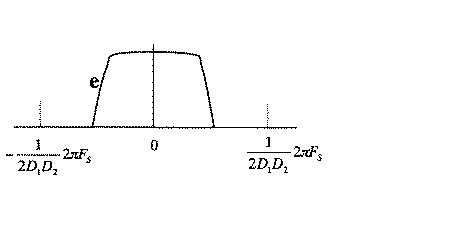
信号dは、第1及び第2の低域フィルタ1035a,1035bによってさらに1/D2にデシメーションされ、第1及び第2の低域フィルタ低域から信号eとして出力される。信号eのサンプリング周波数は(1/D1D2)×2πFSとなる。信号eは、第1及び第2の低域フィルタ1035a,1035bを通過したI,Q信号であり、これらの信号の変化の周波数ドメインは図6に示されている。
なお、IF信号をデシメーションせずに、A/D変換したデータを直接処理すると、大きなハードウェアが必要になる不都合が生じる。
ダウンコンバータ103によりFIRフィルタ処理されたI,Q信号eは、中継部104を経て、アップコンバータ105に入力される。入力信号eは、アップコンバータ105でもFIRフィルタ処理をされ、IF周波数に周波数シフトされ実数のIF信号となり、D/A変換器106へ送られてD/A(デジタル/アナログ)に変換される。
【0018】
アップコンバータ105の動作について図1及び図7〜図11を参照して説明する。
アップコンバータ105の動作は次の条件を満たすものとする。
・入力信号はIを実数部、Qを虚数部とみなせる複素信号である。
そのスペクトラムは図8に示されている。
・少なくとも一段のFIRフィルタを有している。
図7の例では、第1及び第2の低域フィルタ1054a,1054bと、第1及び第2の低域フィルタ1055a,1055bが左右2列に配置され、二段からなるFIRフィルタが形成されている。
・FIRフィルタ又は別の段の低域フィルタ(LPF)と共に、補間処理ができること。
ここで、I,Q信号はサンプリングレートを適当な倍率で上げる。
図7の第1及び第2の低域フィルタ1054a,1054b及び第1及び第2の低域フィルタ1055a,1055bの補間倍率をD1,D2とする。
第1及び第2の低域フィルタ1055a,1055bの出力信号fに関し、図9はI,Q信号eの各サンプルの間にD1−1個の0サンプルを挿入した信号のスペクトラムであり、第1及び第2の低域フィルタ1055a,1055bの特性を点線で描いたものである。
同様に出力信号fは第1及び第2の低域フィルタ(LPF1)1054a,1054bにおいてさらにD1倍に補間され、信号gとして出力される。
図7に示す出力信号gの変化は図10に描かれた周波数ドメインで示されている。
アップコンバータ105の数値制御発振器(NCO)1051の動作は上記ダウンコンバータ103(図2)の数値制御発振器(NCO)1031と同様である。
数値制御発振器1051はIF周波数ωIF=2πFIFに対応して、
cos(ωIFt),sin(ωIFt)
を発生する。
アップコンバータ105の第1及び第2の乗算器1052a,1052bは、上記ダウンコンバータ103と同様に、数値制御発振器1051から発生するsin(ωIFt),cos(ωIFt)とI,Q信号gとを乗算し、それぞれの出力を加算器1057で加算する。
SIF(t)=I(t)・cos(ωIFt)−Q(t)・sin(ωIFt) ・・・式7
式7は、下記の式と同様である。
SIF(t)=Re[I(t)+jQ(t)]exp[−jωIFt]・・・式8
図7に示すアップコンバータ105の出力信号hは式8で表示でき、信号の変化の周波数ドメインは図11で示されている。
アップコンバータ105から出力されたIF信号は式7に示す形で表現でき、式2と同じ形式である。
ダウンコンバータ103から出力されたI,Q信号は、アップコンバータ105でそれぞれフィルタ処理されてからデジタル直交変調器1056で変調され、D/A変換器106によりアナログ信号に変換され、ナイキスト(Nyqist)以上の周波数を制限する低域フィルタ101bを通過してアナログ出力端子107bへ出力される(図1及び図7)。
【0019】
A/D変換器102へ入力される信号が0Hzからある周波数以下に限定された信号の場合において、プログラマブルデジタルフィルタ10の動作は次のとおりである。
この場合には、ダウンコンバータ103は周波数変換を伴なわず、FIRフィルタとして機能する。換言すれば、ダウンコンバータ103における第1段の第1及び第2の低域フィルタ1034a,1034b及び第2段の第1及び第2の低域フィルタ1035a,1035bの部分だけを実行する。
ダウンコンバータ103及びアップコンバータ105を通過する信号に対するフィルタ処理を、それぞれ第1段からなる第1及び第2の低域フィルタ1034a,1034b、第1及び第2の低域フィルタ1054a,1054bのみで行っても良い。
狭帯域のQの高い信号のフィルタ処理を実現しようとすると、アナログ/デジタル変換の速度を落とすことになる(フィルタの負担が増えることになる)。そして低域フィルタ(LPF)のタップ(TAP数)を増やすことになる(回路規模が大きくなる)。
そこで、図2及び図7に示す例では、ダウンコンバータ103及びアップコンバータ105に低域フィルタを2段配置している。入力信号に対して第1段の第1及び第2の低域フィルタ1034a,1034b,1054a,1054bと第2段の第1及び第2の低域フィルタ1035a,1035b,1055a,1055bによる2段階のフィルタ処理を行って、狭帯域で急峻な特性のフィルタが容易に実現できるようにしている。この場合、第1段の低域フィルタ1034a,1034b,1054a,1054bにはCIC(Cascade Integrated Comb Line)フィルタ(櫛型フィルタ)などの高速動作が得意な回路を用い、そして第2段の低域フィルタ1035a,1035b,1055a,1055bにはカスケード型FIRフィルタなどの回路を用いると良い。
【0020】
外部のパーソナルコンピュータ119の役割について説明する。
プログラマブルデジタルフィルタ10に使用される図2及び図7に示す低域フィルタ(LPF1,LPF2)の形式に基づいて、外部のパーソナルコンピュータ119に数個のパラメータを入力させて、係数を求める。上記低域フィルタ(LPF1,LPF2)がナイキストフィルタの場合には、「帯域幅(1/T)」及び「α」の2個のパラメータで求められる。上記低域フィルタ(LPF1,LPF2)がガウスフィルタ(Gauss Filter)の場合には「3dB帯域幅」だけが重要なパラメータである。しかし、サンプリング周波数は、一意的に決定できないので、恣意的に決定する必要がある。
外部のパーソナルコンピュータ119は、IF信号をダウンコンバータ103によってダウンコンバートする際、希望する帯域を任意に選択することができる。
【0021】
ダウンコンバータ103及びアップコンバータ105はFIRフィルタのみ機能させて、全体として、低域フィルタ(LPF)を形成することが可能である。
ダウンコンバータ103における低域フィルタは、図2では第1及び第2の低域フィルタ1034a,1034bと第1及び第2の低域フィルタ1035a,1035bからなる2段に配置されているが、1段でも良い。もちろん、低域フィルタは3段以上の多段に縦接続するようにしても良い。同様に、アップコンバータ105における低域フィルタは、図7では第1及び第2の低域フィルタ1054a,1054bと第1及び第2の低域フィルタ1055a,1055bからなる2段に配置されているが、1段でも良い。もちろん、低域フィルタは3段以上の多段に縦接続するようにしても良い。
ダウンコンバータ103からアップコンバータ105へ送られる信号がシリアル信号であれば、中継部104にシリアルインタフェースを用いる。またパラレル信号であれば、中継部104にFIFO(First In First Out)メモリーのようなメモリー素子を用いる。中継部104がシリアルインタフェースで構成されている場合、回路動作条件は厳しく調整がやや難しいが、回路構成と配線が少なくても済む。また中継部104がFIFOである場合、プログラマブルデジタルフィルタ10の回路は増えるが、動作はシンプルで調整が簡単となるか又は不要となる。また信号の高速処理ができる。
このように、中継部104は、シリアルインタフェース、FIFO(パラレル)などのようなメモリー素子又は伝送路などであっても良い。中継部104が伝送路である場合には、高周波信号はベースバンド信号に変換されて伝送されるから、伝送ノイズが少なく、NF(Noise Figure)の劣化を抑制できる。
制御部111は汎用のマイクロプロセッサ(MPU)でも、またデジタル信号処理器(DSP:Digital Signal Processor)でもどちらでも良い。
【0022】
図12に本発明の第2の実施の形態を示す。
図示するプログラマブルデジタルフィルタ20は、プログラマブルデジタルフィルタ10と実質的に同一構成であるが、複数の数値制御発振器を設け、これらの数値制御発振器に選択的に接続可能である切り替えスイッチを設けている。
以下、プログラマブルデジタルフィルタ20に関して、プログラマブルデジタルフィルタ10と相違する構成部分について説明し、共通する部分について詳細な説明を省略する。
帯域フィルタ(BPF)218、A/D変換器202、D/A変換器206及び低域フィルタ(LPF)201は、プログラマブルデジタルフィルタ10の帯域フィルタ(BPF)118、A/D変換器102、D/A変換器106及び低域フィルタ(LPF)101bに相当している。帯域フィルタ(BPF)218は、A/D変換器202のサンプリング周波数と適合させる。
プログラマブルデジタルフィルタ本体(以下「デジタルフィルタ本体」という。)20Aは、図13に示すように、入力側(図左側)に位置しているデジタル直交変換器であるデジタル直交検波器2036と、出力側(右側)に位置しているデジタル直交変換器であるデジタル直交変調器2056とを備えている。デジタル直交検波器2036とデジタル直交変調器2056との間に複数のフィルタを並列状態に配置してある。
デジタル直交検波器2036の構成及び作用は前記デジタル直交検波器1036のそれらと同様である。デジタル直交検波器2036は、第1の数値制御発振器2031と、第1の数値制御発振器に接続されていると共に、ベースバンドI信号を出力する第1の乗算器2032aと、第1の数値制御発振器に接続されているπ/2位相器2033と、このπ/2位相器に接続されていると共にベースバンドQ信号を出力する第2の乗算器2032bを備えている。デジタル直交検波器2036において、上記ベースバンドI,Q信号に第1の数値制御発振器2031から発生される信号を第1の乗算器2032a及び第2の乗算器2032bによって乗算して周波数変換を行うものである。
デジタル直交変調器2056の構成及び作用は前記デジタル直交変調器1056のそれらと実質的に同様である。デジタル直交変調器2056は、第2の数値制御発振器2051と、第2の数値制御発振器に切り替えスイッチ2058を介して接続可能であると共にベースバンドI信号が入力される第1の乗算器2052aと、切り替えスイッチ2058を介して第2の数値制御発振器2051に接続可能であるπ/2位相器2053と、このπ/2位相器に接続されていると共にベースバンドQ信号が入力される第2の乗算器2052bと、上記第1及び第2の乗算器の出力信号を加算するための加算器2057とを備えている。デジタル直交検波器2036側の第1の数値制御発振器2031は、切り替えスイッチ2058を介してデジタル直交変調器2056側の第1の乗算器2052a及びπ/2位相器2053と接続可能である。
切り替えスイッチ2058は、次の場合に切り換わる。
第1に、切り替えスイッチ2058は、図13に示す入口(Input)からの入力信号の周波数と出口(Output)からの出力信号の周波数が互いに異なる場合、第2の数値制御発振器2051側に切り換わる。
第2に、切り替えスイッチ2058は、上記入力信号と出力信号の周波数が同じ場合、第1の数値制御発振器2031側に切り換わる。
デジタル直交変調器2056の第1及び第2の乗算器2052a,2052bは、上記ベースバンドI,Q信号に第2の数値制御発振器2051から発生される信号を乗算して、加算器2057へ出力することができる。そして第1及び第2の乗算器2052a,2052bは、上記ベースバンドI,Q信号に上記デジタル直交検波器側の第1の数値制御発振器2031から発生される信号を乗算して、加算器2057へ出力することができる。
デジタル直交検波器2036の第1の乗算器2032aから出力されるI信号は、第1乃至第5のフィルタ203a1,203a2,203a3,203a4,203a5を経てデジタル直交変調器2056の第1の乗算器2052aへ入力される。またデジタル直交検波器2036から出力されるQ信号は、第1乃至第5のフィルタ203b1,203b2,203b3,203b4,203b5を経てデジタル直交変調器2056の第2の乗算器2052bへ入力される。第1段の第1及び第2のフィルタ203a1,203b1及び第5段の第1及び第2のフィルタ203a5,203b5には、CICフィルタが使用されている。第2段の第1及び第2のフィルタ203a2,203b2には、第4段の第1及び第2の203a4,203b4にはそれぞれカスケード型FIRフィルタであるCFIRフィルタが使用されている。第3段の第1及び第2のフィルタ203a3,203b3にはプログラマブルFIRフィルタであるPFIRフィルタが使用されている。
【0023】
次に、プログラマブルデジタルフィルタ20の動作について説明する。
まず、デジタルフィルタ本体20Aにおいて、図13に示す入口(Input)からの入力信号の周波数と出口(Output)からの出力信号の周波数が互いに異なる場合について説明する。
この場合には、切り替えスイッチ2058は制御部(図示せず。)によって図13に示す状態に切り替えられて、第2の数値制御発振器2051がオンの状態にセットされる。
この状態で、高周波の入力信号は中間周波のIF信号として帯域フィルタ218に入力される。帯域フィルタ218から帯域制限されて出力されるIF信号は、A/D変換器202に入力され、そこでアナログ/デジタルに変換されてデジタルフィルタ本体20Aに入力される。デジタルIF信号はデジタルフィルタ本体20Aのデジタル直交検波器2036で互いに直交するベースバンドI,Q信号に変換される。そしてベースバンドI信号は第1、第2、第3、第4及び第5のフィルタ203a1,203a2,203a3,203a4,203a5によってフィルタ処理されデジタル直交変調器2056の第1の乗算器2052aに入力される。同時に、ベースバンドQ信号は第1、第2、第3、第4及び第5のフィルタ203b1,203b2,203b3,203b4,203b5によってフィルタ処理されデジタル直交変調器2036の第2の乗算器2052bに入力される。デジタル直交変調器2056において、ベースバンドI,Q信号は周波数変換され、デジタル変調波出力信号となって出口(Output)に向けて出力される。
次に、入口(Input)からの入力信号の周波数と出口(Output)からの出力信号の周波数が同じである場合について説明する。
この場合には、制御部は切り替えスイッチ2058を図13に示す状態すなわち第2の数値制御発振器2051に対してオンとなっている状態からオフの状態に切り替える。このために、第1の数値制御発振器2031はデジタル直交検波器2036及びデジタル直交変調器2056双方の数値制御発振手段として機能する。換言すれば、デジタル直交変調器2056については、第2の数値制御発振器2051に代わる第1の数値制御発振器2031の作動に基づいて周波数変換が行われる。
したがって、デジタルIF信号はデジタルフィルタ本体20Aのデジタル直交検波器2036で互いに直交するベースバンドI,Q信号に変換され、そしてフィルタ203a1〜203a5,203b1〜203b5を介してデジタル直交変調器2056へ入力される。入力信号はデジタル直交変調器2056で上記デジタルIF信号の周波数と同じ周波数のデジタル変調波出力信号となって出口(Output)へ出力される。
デジタルフィルタ本体20Aは、デジタル直交検波器2036とデジタル直交変調器2056の間を図13左右に二分割することにより、図左側がダウンコンバータ203の役割をする部分であり、右側がアップコンバータ205の役割をする部分である。分割する位置はデジタル直交検波器2036とデジタル直交変調器2056の間である限り、図示の例に限られない。
デジタルフィルタ本体20Aは、切り替えスイッチ2058を設けることによって上記2つのケースを選択できる。プログラマブルデジタルフィルタ20の用途は限定されるが、デジタルフィルタ本体における数値制御発振器をデジタル直交検波器2036の第1の数値制御発振器2031とデジタル直交変調器2056の第2の数値制御発振器2051をいずれか一方のもので兼用しても良い。
【0024】
本発明のさらに他の実施の形態について図14を参照して説明する。
プログラマブルデジタルフィルタ30は、プログラマブルデジタルフィルタ10と同一構成のプログラマブルデジタルフィルタ部310を多段(図示の例では3段)に配置しているものである。プログラマブルデジタルフィルタ30は、その入力側がアナログ入力端子107aを介して受信部115に接続されている。
プログラマブルデジタルフィルタ30の出力側は切り替えスイッチ300に接続されている。プログラマブルデジタルフィルタ30には、外部インタフェース114a,114bを介して外部の電子計算機119及び作業部・表示部113にそれぞれ接続されている。プログラマブルデジタルフィルタ30のフィルタ特性変更を外部の電子計算機119及び作業部・表示部113を選択的に用いて操作する。
このように、プログラマブルデジタルフィルタ30を多段(2段以上)の構造にすれば、通信や測定産業などの利用分野に限られず、多くの利用分野において、広い帯域幅の信号を高速処理にすることが可能となり、有益である。
【0025】
図15は、図1に示すプログラマブルデジタルフィルタ10を用いている送信機40の構成を示している。
送信機40において、高周波のIF信号は、本デジタルフィルタシステムであるプログラマブルデジタルフィルタ10を通過する過程で、アナログ信号からデジタル信号に変換され、再びアナログ信号に変換される。そしてアナログ信号はアナログアップコンバータ402でアップコンバートされ、高周波として出力される。
プログラマブルデジタルフィルタ20,30についても、プログラマブルデジタルフィルタ10と同様に、送信機40に適用することができる。
【0026】
図16に示すプログラマブルデジタルフィルタ50において、高周波のIF信号は、シリアル・パラレル変換器502でシリアル信号からパラレル信号に変換されてから、図2に示すダウンコンバータ103と実質的に同一構成のダウンコンバータ503に入力され、A/D変換され、周波数変換され、ベースバンドI,Qの各信号となって出力される。ベースバンドI,Q信号は、アップコンバータ105の代わりに設けているI,Q変調機能をもったデジタル変調信号発生器であるI,Q変調SG(SG:Signal Generator)で変調されてD/A変換されて元の高周波として出力される。
【0027】
広帯域なアナログ信号の高速処理を可能とするプログラマブルデジタルフィルタは、図1、図12及び図14に示すように、デジタルフィルタ本体10A,20A(図1、図12)の入力側にダウンコンバータ103,203(図2、図13)を出力側にアップコンバータ105,205(図7、図13)を配置し、かつこれらのダウンコンバータ及びアップコンバータにデジタル直交検波器1036,2036及びデジタル直交変調器1056,2056を設けることによって実現される。
本発明をデジタル変調信号などの計測システムに適用することにより、特性の異なる等価器(イコライザ)を容易かつ迅速に実現でき、そして多数の変調方式に対応した等価器が実現でき、従来のように個別に回路を持つ必要がなくなる利点がある。
ダウンコンバータ103の代わりに、例えばスペクトラム・アナライザなどを用いても良い。ダウンコンバータ103及びアップコンバータ105のFIR部分を統合したものを、フィールドプログラマブルゲートアレイ(FPGA:Field Programmable Gate Array)で組むようにしても良い。
【0028】
【発明の効果】
本発明によれば、デジタル信号を互いに並列状態に接続されている乗算器で処理するので、周波数変換を従来例に比較して高速化することができ、速い信号処理が可能となるので用途範囲を広げることができる。
【図面の簡単な説明】
【図1】本発明に係るプログラムデジタルシステムを示す構成図である。
【図2】本発明に係るプログラムデジタルシステムにおけるダウンコンバータを拡大して示す構成図である。
【図3】図2に示す各出力信号a,b,b’の変化を周波数ドメインで示す図である。
【図4】図2に示す出力信号cの変化を周波数ドメインで示す図である。
【図5】図2に示す信号dの変化を周波数ドメインで示す図である。
【図6】図2に示す信号eの変化を周波数ドメインで示す図である。
【図7】本発明に係るプログラムデジタルシステムにおけるアップコンバータを拡大して示す構成図である。
【図8】図7に示す信号eの変化を周波数ドメインで示す図である。
【図9】図7に示す信号fの変化を周波数ドメインで示す図である。
【図10】図7に示す信号gの変化を周波数ドメインで示す図である。
【図11】図7に示す信号hの変化を周波数ドメインで示す図である。
【図12】本発明の別のプログラマブルデジタルフィルタを示すブロック図である。
【図13】図12に示すデジタルフィルタ本体を拡大して示す構成図である。
【図14】本発明のさらに別のプログラマブルデジタルフィルタを示す構成図である。
【図15】本発明を適用した送信機のブロック図である。
【図16】本発明の別のプログラマブルデジタルフィルタを示すブロック図である。
【符号の説明】
10 プログラマブルデジタルフィルタ
10A プログラマブルデジタルフィルタ本体
101a 低域フィルタ(LPF)
101b 低域フィルタ(LPF)
102 A/D変換器
103 デジタルダウンコンバータ(DDC)
105 デジタルアップコンバータ(DUC)
106 D/A変換器
108 減衰器
109 増幅器
1031 数値制御発振器(NCO)
1032a 第1の乗算器
1032b 第2の乗算器
1033 π/2位相器
1034a 第1の低域フィルタ(LPF1)
1034b 第2の低域フィルタ(LPF1)
1035a 第1の低域フィルタ(LPF2)
1035b 第2の低域フィルタ(LPF2)
1036 デジタル直交検波器(デジタル直交変換器)
1051 数値制御発振器(NCO)
1052a 第1の乗算器
1052b 第2の乗算器
1053 π/2位相器
1054a 第1の低域フィルタ(LPF1)
1054b 第2の低域フィルタ(LPF1)
1055a 第1の低域フィルタ(LPF2)
1055b 第2の低域フィルタ(LPF2)
1056 デジタル直交変調器(デジタル直交変換器)
1057 加算器
20 プログラマブルデジタルフィルタ
20A プログラマブルデジタルフィルタ本体
201 低域フィルタ(LPF)
202 A/D変換器
203 デジタルダウンコンバータ
205 デジタルアップコンバータ
206 D/A変換器
218 帯域フィルタ(BPF)
2032a 第1の乗算器
2032b 第2の乗算器
2033 π/2位相器
203a1 第1のフィルタ(CIC)
203a2 第2のフィルタ(CFIR)
203a3 第3のフィルタ(PFIR)
203a4 第4のフィルタ(CFIR)
203a5 第5のフィルタ(CIC)
203b1 第1のフィルタ(CIC)
203b2 第2のフィルタ(CFIR)
203b3 第3のフィルタ(PFIR)
203b4 第4のフィルタ(CFIR)
203b5 第5のフィルタ(CIC)
2031 第1の数値制御発振器(NCO)
2036 デジタル直交検波器(デジタル直交変換器)
2051 第2の数値制御発振器(NCO)
2052a 第1の乗算器
2052b 第2の乗算器
2053 π/2位相器
2056 デジタル直交変調器(デジタル直交変換器)
2057 加算器
2058 切り替えスイッチ
30 プログラマブルデジタルフィルタ
310 プログラマブルデジタルフィルタ部
503 デジタルダウンコンバータ[0001]
BACKGROUND OF THE INVENTION
The present invention relates to a digital orthogonal transformer used in a digital communication device, a measurement device, a radar, and the like.
[0002]
[Prior art]
As an orthogonal transformer, for example, a demodulator described in Japanese Patent Laid-Open No. 2002-9862 has been proposed. This demodulator is incorporated in a digital wireless communication apparatus, and includes a local oscillator, a phase shifter, and two multipliers. The local oscillator generates a signal having substantially the same frequency as the intermediate frequency input signal (analog signal) supplied from the receiver, and outputs the signal to one multiplier and the phase shifter.
The phase shifter shifts the phase of the signal from the local oscillator by 90 ° and supplies it to the other multiplier. Both multipliers multiply each input signal by the signal from the local oscillator and the signal from the phase shifter, and output an I signal and a Q signal as orthogonal components of the input signal that are orthogonal to each other. The output I signal and Q signal are each converted from an analog signal to a digital signal by an A / D converter.
[0003]
[Problems to be solved by the invention]
Since the demodulator described above separates an input analog signal into an I signal and a Q signal by an analog circuit, the signal processing takes time, and there is a limit to increase the processing speed. For example, there is a problem that cannot be used for a digital filter that requires high-speed processing.
SUMMARY OF THE INVENTION An object of the present invention is to provide a digital orthogonal transformer that enables high-speed signal processing and expands the application range.
[0004]
[Means for Solving the Problems]
A first feature of the present invention is a digital orthogonal transformer that converts an input digital signal into orthogonal baseband I and Q signals that are 90 ° out of phase with each other. A first multiplier for outputting the baseband I signal, and a second multiplier for outputting a baseband Q signal connected to the numerically controlled oscillator via a π / 2 phase shifter; It is in having. The first multiplier and the second multiplier are connected in parallel to each other on the input side, and multiply each of the input digital signals by a signal generated from the numerically controlled oscillator to generate a baseband I, The signal is converted to a Q signal.
According to a second feature of the present invention, on the premise of the first feature, a digital filter for band-limiting baseband I and Q signals on the output side of the first multiplier and the second multiplier, respectively. It is located.
A third feature of the present invention is a digital for band-limiting baseband I and Q signals on the output side of the first multiplier and the second multiplier on the premise of the first or second feature. Filters are arranged, and each digital filter is a low-pass filter.
A fourth feature of the present invention is a digital for band-limiting baseband I and Q signals on the output side of the first multiplier and the second multiplier on the premise of the first or second feature. Filters are arranged, and each digital filter is an FIR filter.
According to a fifth feature of the present invention, on the premise of any of the first to fourth features, baseband I and Q signals are band-limited to the output side of the first multiplier and the second multiplier, respectively. Therefore, a plurality of digital filters are arranged.
A sixth feature of the present invention is that an A / D converter connected to the input side of the first multiplier and the second multiplier on the premise of any one of the first to fifth features. It is in having been arranged.
A seventh feature of the present invention is that an A / D converter connected to the input side of the first multiplier and the second multiplier on the premise of any one of the first to fifth features. An attenuator and an amplifier are arranged on the input side of the A / D converter, and the attenuator and the amplifier hold the level of the signal input to the A / D converter. is there.
The eighth feature of the present invention is that it comprises a digital quadrature detector that converts input digital signals into orthogonal baseband I and Q signals that are 90 ° out of phase with each other, and a digital quadrature modulator. is there. The digital quadrature detector includes a numerically controlled oscillator, a first multiplier and a second multiplier connected in parallel with each other on the input side, and a π / 2 phase shifter. The second multiplier multiplies the input digital signal by the signal generated from the numerically controlled oscillator, and the second multiplier multiplies the input digital signal by the signal generated from the numerically controlled oscillator. To do. The digital quadrature modulator includes a numerically controlled oscillator, a first multiplier to which a baseband I signal is input and connected to the numerically controlled oscillator, and a π / 2 phase connected to the numerically controlled oscillator. A second multiplier that receives a baseband Q signal and is connected to the numerically controlled oscillator via a π / 2 phase shifter, and an output side of each of the first and second multipliers. And the first and second multipliers multiply the baseband I and Q signals by the signal generated from the numerically controlled oscillator, and the adder The output signals of the first and second multipliers are added.
According to a ninth feature of the present invention, there is provided a digital filter for band-limiting the baseband I and Q signals output from the first and second multipliers of the digital quadrature detector on the premise of the eighth feature. Each of them is located.
According to a tenth feature of the present invention, on the premise of the eighth or ninth feature, the numerically controlled oscillator of the digital quadrature detector is connected to the first multiplier of the digital quadrature modulator and the π / 2 phase via a changeover switch. The numerically controlled oscillator of the digital quadrature detector can be connected to and separated from the changeover switch.
[0005]
DETAILED DESCRIPTION OF THE INVENTION
An example in which the digital orthogonal transformer according to the present invention is used as a programmable digital filter will be described with reference to the drawings.
A programmable
An attenuator (ATT) 108 and an amplifier (AMP) 109 are arranged between the low-pass filter 101a located at the left end of FIG. 1 and the
The
As shown in FIG. 2, the
[0006]
The low-pass filter 101a on the left side of FIG. 1 has the following three functions.
The first is a function as an anti-aliasing filter for the A /
The second function is a band filter (BPF) for the
The third function is to pass the input signal as it is when the low-pass filter 101a is inappropriate in relation to the A / D converter because the A /
[0007]
The A /
The IF signal is input to the
[0008]
The configuration of the
The down-
A digital quadrature detector (orthogonal demodulator) 1036 in the
Low-pass filters (LPFs) arranged in a plurality of stages are connected to the
The
However, when the input signal a is limited to a predetermined frequency, for example, from 0 Hz to a certain frequency or less, the down-
The frequency domain in the change of each signal a, b, b ′, c, d, and e shown in FIGS. 2 and 3 to 6 will be described later.
The signals (I and Q signals) b and b ′ output from the first and
An output signal e of the
[0009]
As shown in FIG. 1, the
[0010]
The configuration of the
The up-
The up-
In the
The up-
Each frequency domain in the change of each signal e, f, g, h shown in FIGS. 7 and 8 to 11 will be described later.
[0011]
The D /
[0012]
An output-side low-pass filter (LPF) 101 b located at the right end of FIG. 1 removes harmonics due to sampling from the output of the D /
[0013]
As shown in FIG. 1, the attenuator 108 (ATT) and the amplifier (AMP) 109 adjust the level of the input signal from the
[0014]
The
The
Using the working unit in the working unit /
The
The connection method of the
When many programs for changing the characteristics of the filter system are stored in the
[0015]
Next, the operation of the programmable
The frequency range of the high frequency input signal from the
The bandwidth of the input signal from the
As shown in FIGS. 1 and 2, the analog signal is received by the receiving
As described above, since the dynamic range of the A /
For the down-
[0016]
The signal input to the A /
Hereinafter, an operation when the frequency of the input signal is not limited to a frequency below 0 Hz will be described.
The operation when the input signal is limited to a frequency below 0 Hz will be described later.
The A /
The down
That is, in the
As described above, the IF signal input to the
[0017]
Further, a specific operation of the
- the sampling frequency of the A /
The signal a input to the
The center frequency of the input signal a is IF frequency, and F IF (Hz), ω IF = 2πF IF (angular frequency).
Under the above conditions, generally, the band-limited IF signal can be considered as the real part of the complex signal I + jQ multiplied by exp [jω IF ].
The IF signal is expressed by
{I (t) + jQ ( t)} × exp [jω IF] = {Icos (ω IF t) -Qsin (ω IF t)} + j {Isin (ω IF t) + Qcos (ω IF t)} ···
The real part is given by
I cos (ω IF t) −Q sin (ω IF t)
The signal a discretized by the A /
FIG. 3 shows changes in the signals a, b, and b ′ at each stage of the
4 to 6 depict changes in the signals c, d, and e at each stage of the
An input signal a of the
A numerically controlled oscillator (NCO) 1031 of the
Will occur.
However, F S > 2F IF Formula 4-1
The time t is discretized and is an integer multiple of the quantized time unit Δt t = Δt × i Equation 4-2
And Hereinafter, Expression 4-2 is simply described as t.
Means for multiplying
The frequency domains of the output signals b and b ′ of the first and
Expressions 5 and 6 have two frequency components of I and Q themselves and those multiplied by 2ω IF . If this is multiplied by the first and second low-
−1/2 {Qcos (θ 0 ) −Isin (θ 0 )} Equation 6B
It becomes.
Equation 6A and Equation 6B are
1/2 (I−jQ) × {cos (θ 0 ) + jsin (θ 0 )}
Correspond to the real part and imaginary part respectively. That is, the real part and imaginary part of I + jQ obtained by phase rotation.
Equations 6A and 6B are so-called “baseband signals” in the output signal c shown in FIG. The change of the output signal c is depicted in the frequency domain shown in FIG.
The output sampling frequencies of the first stage first and second low-
For example, the decimation rate of the first-stage first and second low-
It can be considered that the IF signal is converted by the A /
Signal c shown in FIG. 2, the first stage the first and second low-
Further, the output signal d shown in FIG. 2 is in the process in which the signal c decimated to 1 / D 1 is processed by the first and second low-
The signal d is further decimated to 1 / D 2 by the first and second low-
If the A / D converted data is directly processed without decimation of the IF signal, there is a disadvantage that a large amount of hardware is required.
The I and Q signals e subjected to the FIR filter processing by the
[0018]
The operation of the up-
It is assumed that the operation of the up-
-The input signal is a complex signal in which I can be regarded as a real part and Q as an imaginary part.
Its spectrum is shown in FIG.
-It has at least one FIR filter.
In the example of FIG. 7, the first and second low-
-Interpolation processing can be performed together with the FIR filter or another low-pass filter (LPF).
Here, the I and Q signals increase the sampling rate by an appropriate magnification.
First and second low-
Regarding the output signal f of the first and second low-
Similarly, the output signal f of the first and second low-pass filter (LPF1) 1054a, are interpolated to further 1x D at 1054b, is output as a signal g.
The change of the output signal g shown in FIG. 7 is shown in the frequency domain depicted in FIG.
The operation of the numerically controlled oscillator (NCO) 1051 of the
The numerically controlled
cos (ω IF t), sin (ω IF t)
Is generated.
The first and
S IF (t) = I (t) · cos (ω IF t) −Q (t) · sin (ω IF t) Equation 7
Expression 7 is the same as the following expression.
S IF (t) = Re [I (t) + jQ (t)] exp [−jω IF t] Equation 8
The output signal h of the up-
The IF signal output from the up-
The I and Q signals output from the
[0019]
In the case where the signal input to the A /
In this case, the
Filter processing for signals passing through the down-
If filtering of a narrow band high Q signal is realized, the analog / digital conversion speed is reduced (the burden on the filter increases). Then, the number of taps (TAP number) of the low-pass filter (LPF) is increased (the circuit scale is increased).
Therefore, in the example shown in FIGS. 2 and 7, two stages of low-pass filters are arranged in the
[0020]
The role of the external
Based on the low-pass filters (LPF1, LPF2) shown in FIG. 2 and FIG. 7 used for the programmable
The external
[0021]
The down-
In FIG. 2, the low-pass filter in the
If the signal sent from the
As described above, the
The
[0022]
FIG. 12 shows a second embodiment of the present invention.
The programmable
Hereinafter, regarding the programmable
The band-pass filter (BPF) 218, the A /
As shown in FIG. 13, a programmable digital filter main body (hereinafter referred to as “digital filter main body”) 20A includes a
The configuration and operation of the
The configuration and operation of the digital quadrature modulator 2056 are substantially the same as those of the
The
First, when the frequency of the input signal from the input and the output signal from the output shown in FIG. 13 are different from each other, the
Secondly, the
The first and
The I signal output from the
[0023]
Next, the operation of the programmable
First, in the digital filter
In this case, the
In this state, the high frequency input signal is input to the
Next, the case where the frequency of the input signal from the input (Input) and the frequency of the output signal from the output (Output) are the same will be described.
In this case, the control unit switches the
Therefore, the digital IF signal is converted into baseband I and Q signals orthogonal to each other by the
The digital filter
The
[0024]
Still another embodiment of the present invention will be described with reference to FIG.
The programmable digital filter 30 is configured by arranging the programmable
The output side of the programmable digital filter 30 is connected to the
Thus, if the programmable digital filter 30 has a multi-stage (two or more stages) structure, it is not limited to fields of use such as the communication and measurement industries, and a wide bandwidth signal can be processed at high speed in many fields of use. Is possible and beneficial.
[0025]
FIG. 15 shows a configuration of the transmitter 40 using the programmable
In the transmitter 40, the high-frequency IF signal is converted from an analog signal to a digital signal in the process of passing through the programmable
Similarly to the programmable
[0026]
In the programmable
[0027]
As shown in FIGS. 1, 12, and 14, the programmable digital filter that enables high-speed processing of a wideband analog signal includes a down-
By applying the present invention to a measurement system such as a digital modulation signal, an equalizer with different characteristics can be realized easily and quickly, and an equalizer corresponding to a large number of modulation methods can be realized. There is an advantage that it is not necessary to have a separate circuit.
Instead of the
[0028]
【The invention's effect】
According to the present invention, since digital signals are processed by multipliers connected in parallel to each other, frequency conversion can be speeded up compared to the conventional example, and fast signal processing is possible, so Can be spread.
[Brief description of the drawings]
FIG. 1 is a block diagram showing a program digital system according to the present invention.
FIG. 2 is an enlarged configuration diagram showing a down converter in the program digital system according to the present invention.
FIG. 3 is a diagram showing changes in output signals a, b, and b ′ shown in FIG. 2 in the frequency domain.
FIG. 4 is a diagram showing changes in the output signal c shown in FIG. 2 in the frequency domain.
FIG. 5 is a diagram showing a change in the signal d shown in FIG. 2 in the frequency domain.
6 is a diagram showing a change in the signal e shown in FIG. 2 in the frequency domain. FIG.
FIG. 7 is an enlarged configuration diagram showing an up-converter in the program digital system according to the present invention.
FIG. 8 is a diagram showing a change in the signal e shown in FIG. 7 in the frequency domain.
FIG. 9 is a diagram showing a change in the signal f shown in FIG. 7 in the frequency domain.
FIG. 10 is a diagram showing a change in the signal g shown in FIG. 7 in the frequency domain.
11 is a diagram showing a change in the signal h shown in FIG. 7 in the frequency domain. FIG.
FIG. 12 is a block diagram illustrating another programmable digital filter of the present invention.
13 is an enlarged configuration diagram of the digital filter main body shown in FIG. 12. FIG.
FIG. 14 is a block diagram showing still another programmable digital filter of the present invention.
FIG. 15 is a block diagram of a transmitter to which the present invention is applied.
FIG. 16 is a block diagram illustrating another programmable digital filter of the present invention.
[Explanation of symbols]
10 Programmable
101b Low-pass filter (LPF)
102 A /
105 Digital Up Converter (DUC)
106 D /
1032a
1034b Second low-pass filter (LPF1)
1035a First low-pass filter (LPF2)
1035b Second low-pass filter (LPF2)
1036 Digital quadrature detector (digital quadrature transformer)
1051 Numerically controlled oscillator (NCO)
1052a
1054b Second low-pass filter (LPF1)
1055a First low-pass filter (LPF2)
1055b Second low-pass filter (LPF2)
1056 Digital quadrature modulator (digital quadrature converter)
1057
202 A /
2032a
203a2 Second filter (CFIR)
203a3 Third filter (PFIR)
203a4 Fourth filter (CFIR)
203a5 Fifth filter (CIC)
203b1 first filter (CIC)
203b2 second filter (CFIR)
203b3 Third filter (PFIR)
203b4 Fourth filter (CFIR)
203b5 fifth filter (CIC)
2031 First numerically controlled oscillator (NCO)
2036 Digital Quadrature Detector (Digital Quadrature Transformer)
2051 Second numerically controlled oscillator (NCO)
2052a
2057
Claims (10)
数値制御発振器と、この数値制御発振器に接続されていると共に、上記ベースバンドI信号を出力する第1の乗算器と、上記数値制御発振器にπ/2位相器を介して接続されベースバンドQ信号を出力する第2の乗算器とを備え、
上記第1の乗算器及び第2の乗算器は互いに入力側で並列的に接続されており、それぞれが入力されるデジタル信号に上記数値制御発振器から発生される信号を乗算してベースバンドI,Q信号に変換することを特徴とするデジタル直交変換器。A digital orthogonal converter that converts input digital signals into orthogonal baseband I and Q signals that are 90 ° out of phase with each other;
A numerically controlled oscillator, a first multiplier connected to the numerically controlled oscillator and outputting the baseband I signal, and a baseband Q signal connected to the numerically controlled oscillator via a π / 2 phase shifter A second multiplier for outputting
The first multiplier and the second multiplier are connected in parallel to each other on the input side, and multiply each of the input digital signals by a signal generated from the numerically controlled oscillator to generate a baseband I, A digital orthogonal transformer characterized by converting into a Q signal.
上記デジタル直交検波器は、数値制御発振器と、互いに入力側で並列状態に接続されている第1の乗算器及び第2の乗算器と、π/2位相器とを備えており、上記第1の乗算器は入力されるデジタル信号に上記数値制御発振器から発生される信号を乗算するものであり、上記第2の乗算器は入力されるデジタル信号に上記数値制御発振器から発生される信号を乗算するものであり、
上記デジタル直交変調器は、数値制御発振器と、ベースバンドI信号が入力されると共に上記数値制御発振器に接続されている第1の乗算器と、上記数値制御発振器に接続されているπ/2位相器と、ベースバンドQ信号が入力されると共に上記数値制御発振器にπ/2位相器を介して接続されている第2の乗算器と、上記第1及び第2の乗算器の出力側のそれぞれに接続されている加算器とを備えており、上記第1及び第2の乗算器はベースバンドI,Q信号に上記数値制御発振器から発生される信号を乗算するものであり、上記加算器は上記第1及び第2の乗算器の出力信号を加算するものであることを特徴とするデジタル直交変換器。A digital quadrature detector that converts the input digital signals into orthogonal baseband I and Q signals that are 90 ° out of phase with each other, and a digital quadrature modulator,
The digital quadrature detector includes a numerically controlled oscillator, a first multiplier and a second multiplier connected in parallel with each other on the input side, and a π / 2 phase shifter. The second multiplier multiplies the input digital signal by the signal generated from the numerically controlled oscillator, and the second multiplier multiplies the input digital signal by the signal generated from the numerically controlled oscillator. Is what
The digital quadrature modulator includes a numerically controlled oscillator, a first multiplier to which a baseband I signal is input and connected to the numerically controlled oscillator, and a π / 2 phase connected to the numerically controlled oscillator. A second multiplier that receives a baseband Q signal and is connected to the numerically controlled oscillator via a π / 2 phase shifter, and an output side of each of the first and second multipliers. And the first and second multipliers multiply the baseband I and Q signals by the signal generated from the numerically controlled oscillator, and the adder A digital orthogonal transformer characterized by adding output signals of the first and second multipliers.
Priority Applications (1)
| Application Number | Priority Date | Filing Date | Title |
|---|---|---|---|
| JP2003186466A JP2005020675A (en) | 2003-06-30 | 2003-06-30 | Digital quadrature convertor |
Applications Claiming Priority (1)
| Application Number | Priority Date | Filing Date | Title |
|---|---|---|---|
| JP2003186466A JP2005020675A (en) | 2003-06-30 | 2003-06-30 | Digital quadrature convertor |
Publications (1)
| Publication Number | Publication Date |
|---|---|
| JP2005020675A true JP2005020675A (en) | 2005-01-20 |
Family
ID=34185580
Family Applications (1)
| Application Number | Title | Priority Date | Filing Date |
|---|---|---|---|
| JP2003186466A Pending JP2005020675A (en) | 2003-06-30 | 2003-06-30 | Digital quadrature convertor |
Country Status (1)
| Country | Link |
|---|---|
| JP (1) | JP2005020675A (en) |
Cited By (7)
| Publication number | Priority date | Publication date | Assignee | Title |
|---|---|---|---|---|
| JP2008259207A (en) * | 2007-03-31 | 2008-10-23 | Sony Deutsche Gmbh | Digital filter |
| JP2010525758A (en) * | 2007-04-23 | 2010-07-22 | ダリ システムズ カンパニー リミテッド | Digital hybrid mode power amplifier system |
| JP2012028883A (en) * | 2010-07-21 | 2012-02-09 | Anritsu Corp | Error rate measuring apparatus and error rate measuring method |
| US11129076B2 (en) | 2006-12-26 | 2021-09-21 | Dali Wireless, Inc. | Method and system for baseband predistortion linearization in multi-channel wideband communication systems |
| US11159129B2 (en) | 2002-05-01 | 2021-10-26 | Dali Wireless, Inc. | Power amplifier time-delay invariant predistortion methods and apparatus |
| US11418155B2 (en) | 2002-05-01 | 2022-08-16 | Dali Wireless, Inc. | Digital hybrid mode power amplifier system |
| US20220295487A1 (en) | 2010-09-14 | 2022-09-15 | Dali Wireless, Inc. | Remotely reconfigurable distributed antenna system and methods |
-
2003
- 2003-06-30 JP JP2003186466A patent/JP2005020675A/en active Pending
Cited By (9)
| Publication number | Priority date | Publication date | Assignee | Title |
|---|---|---|---|---|
| US11159129B2 (en) | 2002-05-01 | 2021-10-26 | Dali Wireless, Inc. | Power amplifier time-delay invariant predistortion methods and apparatus |
| US11418155B2 (en) | 2002-05-01 | 2022-08-16 | Dali Wireless, Inc. | Digital hybrid mode power amplifier system |
| US11129076B2 (en) | 2006-12-26 | 2021-09-21 | Dali Wireless, Inc. | Method and system for baseband predistortion linearization in multi-channel wideband communication systems |
| US11818642B2 (en) | 2006-12-26 | 2023-11-14 | Dali Wireless, Inc. | Distributed antenna system |
| JP2008259207A (en) * | 2007-03-31 | 2008-10-23 | Sony Deutsche Gmbh | Digital filter |
| JP2010525758A (en) * | 2007-04-23 | 2010-07-22 | ダリ システムズ カンパニー リミテッド | Digital hybrid mode power amplifier system |
| JP2012028883A (en) * | 2010-07-21 | 2012-02-09 | Anritsu Corp | Error rate measuring apparatus and error rate measuring method |
| US20220295487A1 (en) | 2010-09-14 | 2022-09-15 | Dali Wireless, Inc. | Remotely reconfigurable distributed antenna system and methods |
| US11805504B2 (en) | 2010-09-14 | 2023-10-31 | Dali Wireless, Inc. | Remotely reconfigurable distributed antenna system and methods |
Similar Documents
| Publication | Publication Date | Title |
|---|---|---|
| US6421534B1 (en) | Integrated frequency translation and selectivity | |
| US9455756B2 (en) | Systems and methods for frequency independent analog self-interference cancellation | |
| JP5902430B2 (en) | Harmonic rejection receiver architecture and mixer | |
| JP3545606B2 (en) | Receiver | |
| US7295826B1 (en) | Integrated frequency translation and selectivity with gain control functionality, and applications thereof | |
| JP3414633B2 (en) | Frequency converter | |
| US7146148B2 (en) | Low intermediate frequency type receiver | |
| JP2005348403A (en) | Digital filter using frequency conversion and method thereof | |
| JP2005020675A (en) | Digital quadrature convertor | |
| JP2001230695A (en) | Radio equipment and frequency conversion method to be used therefor | |
| JP2005020659A (en) | Programmable digital filter | |
| KR20030058146A (en) | Receiver of eliminating image signal | |
| JP5890852B2 (en) | Mobile terminal test apparatus and test method | |
| JP5546999B2 (en) | Radar equipment | |
| JP2003283255A (en) | Direct detection circuit | |
| JP3376454B2 (en) | Signal analyzer | |
| JP3828077B2 (en) | Frequency conversion circuit and communication device | |
| CN1487709B (en) | data receiving device | |
| JP2010130185A (en) | Sampling rate conversion circuit | |
| KR20040013328A (en) | Apparatus for reducing the dc offset of direct conversion receiver | |
| JP5354750B2 (en) | Receiver, program and method using undersampling to remove image signal | |
| JP2000338226A (en) | Radar equipment | |
| CN116359871B (en) | Signal processing method and image acquisition equipment | |
| Rodrigues et al. | Generation and analysis of vestigial side band signals | |
| EP4474834A1 (en) | Spectrum analyzer device and procedures for operating a spectrum analyzer device |
Legal Events
| Date | Code | Title | Description |
|---|---|---|---|
| A621 | Written request for application examination |
Free format text: JAPANESE INTERMEDIATE CODE: A621 Effective date: 20060602 |
|
| A977 | Report on retrieval |
Free format text: JAPANESE INTERMEDIATE CODE: A971007 Effective date: 20080827 |
|
| A131 | Notification of reasons for refusal |
Free format text: JAPANESE INTERMEDIATE CODE: A131 Effective date: 20080930 |
|
| A02 | Decision of refusal |
Free format text: JAPANESE INTERMEDIATE CODE: A02 Effective date: 20090310 |