JP2004359867A - Insulation resin composition, prepreg produced by using the same, conductor foil with resin, conductor-clad laminated board and method for producing multilayer circuit board - Google Patents
Insulation resin composition, prepreg produced by using the same, conductor foil with resin, conductor-clad laminated board and method for producing multilayer circuit board Download PDFInfo
- Publication number
- JP2004359867A JP2004359867A JP2003161189A JP2003161189A JP2004359867A JP 2004359867 A JP2004359867 A JP 2004359867A JP 2003161189 A JP2003161189 A JP 2003161189A JP 2003161189 A JP2003161189 A JP 2003161189A JP 2004359867 A JP2004359867 A JP 2004359867A
- Authority
- JP
- Japan
- Prior art keywords
- resin composition
- conductor
- insulating resin
- compound
- wiring board
- Prior art date
- Legal status (The legal status is an assumption and is not a legal conclusion. Google has not performed a legal analysis and makes no representation as to the accuracy of the status listed.)
- Pending
Links
- 239000011342 resin composition Substances 0.000 title claims abstract description 87
- 239000011888 foil Substances 0.000 title claims abstract description 82
- 239000004020 conductor Substances 0.000 title claims abstract description 79
- 229920005989 resin Polymers 0.000 title claims description 83
- 239000011347 resin Substances 0.000 title claims description 83
- 238000004519 manufacturing process Methods 0.000 title claims description 14
- 238000009413 insulation Methods 0.000 title abstract description 4
- 150000001875 compounds Chemical class 0.000 claims abstract description 61
- 229920000647 polyepoxide Polymers 0.000 claims abstract description 49
- 239000003822 epoxy resin Substances 0.000 claims abstract description 47
- ISWSIDIOOBJBQZ-UHFFFAOYSA-N phenol group Chemical group C1(=CC=CC=C1)O ISWSIDIOOBJBQZ-UHFFFAOYSA-N 0.000 claims abstract description 47
- -1 aromatic carboxylic acid halide Chemical class 0.000 claims abstract description 23
- WPYMKLBDIGXBTP-UHFFFAOYSA-N benzoic acid Chemical compound OC(=O)C1=CC=CC=C1 WPYMKLBDIGXBTP-UHFFFAOYSA-N 0.000 claims abstract description 15
- 125000003700 epoxy group Chemical group 0.000 claims abstract description 6
- 125000000962 organic group Chemical group 0.000 claims description 21
- 239000012212 insulator Substances 0.000 claims description 19
- 239000000758 substrate Substances 0.000 claims description 19
- 125000003118 aryl group Chemical group 0.000 claims description 16
- 125000002887 hydroxy group Chemical group [H]O* 0.000 claims description 16
- 238000010030 laminating Methods 0.000 claims description 15
- 238000010438 heat treatment Methods 0.000 claims description 12
- 150000001299 aldehydes Chemical class 0.000 claims description 6
- 238000009833 condensation Methods 0.000 claims description 6
- 230000005494 condensation Effects 0.000 claims description 6
- 238000000059 patterning Methods 0.000 claims description 6
- 125000004464 hydroxyphenyl group Chemical group 0.000 claims description 5
- 150000002576 ketones Chemical class 0.000 claims description 5
- PSHKMPUSSFXUIA-UHFFFAOYSA-N n,n-dimethylpyridin-2-amine Chemical group CN(C)C1=CC=CC=N1 PSHKMPUSSFXUIA-UHFFFAOYSA-N 0.000 claims description 5
- 125000004435 hydrogen atom Chemical group [H]* 0.000 claims description 4
- 125000001997 phenyl group Chemical group [H]C1=C([H])C([H])=C(*)C([H])=C1[H] 0.000 claims description 3
- 125000001570 methylene group Chemical group [H]C([H])([*:1])[*:2] 0.000 claims description 2
- 238000006243 chemical reaction Methods 0.000 abstract description 11
- IISBACLAFKSPIT-UHFFFAOYSA-N bisphenol A Chemical compound C=1C=C(O)C=CC=1C(C)(C)C1=CC=C(O)C=C1 IISBACLAFKSPIT-UHFFFAOYSA-N 0.000 description 31
- 229920003986 novolac Polymers 0.000 description 27
- SMQUZDBALVYZAC-UHFFFAOYSA-N salicylaldehyde Chemical compound OC1=CC=CC=C1C=O SMQUZDBALVYZAC-UHFFFAOYSA-N 0.000 description 22
- 238000000034 method Methods 0.000 description 19
- CSCPPACGZOOCGX-UHFFFAOYSA-N Acetone Chemical compound CC(C)=O CSCPPACGZOOCGX-UHFFFAOYSA-N 0.000 description 18
- RYGMFSIKBFXOCR-UHFFFAOYSA-N Copper Chemical compound [Cu] RYGMFSIKBFXOCR-UHFFFAOYSA-N 0.000 description 16
- 239000000047 product Substances 0.000 description 14
- 239000011889 copper foil Substances 0.000 description 12
- 238000005553 drilling Methods 0.000 description 9
- 239000000463 material Substances 0.000 description 9
- ZWEHNKRNPOVVGH-UHFFFAOYSA-N 2-Butanone Chemical compound CCC(C)=O ZWEHNKRNPOVVGH-UHFFFAOYSA-N 0.000 description 8
- 238000001644 13C nuclear magnetic resonance spectroscopy Methods 0.000 description 7
- 239000002904 solvent Substances 0.000 description 7
- 238000001228 spectrum Methods 0.000 description 7
- WSFSSNUMVMOOMR-UHFFFAOYSA-N Formaldehyde Chemical compound O=C WSFSSNUMVMOOMR-UHFFFAOYSA-N 0.000 description 6
- OKKJLVBELUTLKV-UHFFFAOYSA-N Methanol Chemical compound OC OKKJLVBELUTLKV-UHFFFAOYSA-N 0.000 description 6
- YXFVVABEGXRONW-UHFFFAOYSA-N Toluene Chemical compound CC1=CC=CC=C1 YXFVVABEGXRONW-UHFFFAOYSA-N 0.000 description 6
- ZMANZCXQSJIPKH-UHFFFAOYSA-N Triethylamine Chemical compound CCN(CC)CC ZMANZCXQSJIPKH-UHFFFAOYSA-N 0.000 description 6
- PXKLMJQFEQBVLD-UHFFFAOYSA-N bisphenol F Chemical compound C1=CC(O)=CC=C1CC1=CC=C(O)C=C1 PXKLMJQFEQBVLD-UHFFFAOYSA-N 0.000 description 6
- 239000011521 glass Substances 0.000 description 6
- 239000000853 adhesive Substances 0.000 description 5
- 230000001070 adhesive effect Effects 0.000 description 5
- 230000015572 biosynthetic process Effects 0.000 description 5
- 238000005530 etching Methods 0.000 description 5
- 230000009477 glass transition Effects 0.000 description 5
- 238000000465 moulding Methods 0.000 description 5
- 238000003825 pressing Methods 0.000 description 5
- 238000007788 roughening Methods 0.000 description 5
- 239000002966 varnish Substances 0.000 description 5
- QTWJRLJHJPIABL-UHFFFAOYSA-N 2-methylphenol;3-methylphenol;4-methylphenol Chemical compound CC1=CC=C(O)C=C1.CC1=CC=CC(O)=C1.CC1=CC=CC=C1O QTWJRLJHJPIABL-UHFFFAOYSA-N 0.000 description 4
- VPWNQTHUCYMVMZ-UHFFFAOYSA-N 4,4'-sulfonyldiphenol Chemical compound C1=CC(O)=CC=C1S(=O)(=O)C1=CC=C(O)C=C1 VPWNQTHUCYMVMZ-UHFFFAOYSA-N 0.000 description 4
- IJGRMHOSHXDMSA-UHFFFAOYSA-N Atomic nitrogen Chemical compound N#N IJGRMHOSHXDMSA-UHFFFAOYSA-N 0.000 description 4
- 239000004593 Epoxy Substances 0.000 description 4
- YCIMNLLNPGFGHC-UHFFFAOYSA-N catechol Chemical compound OC1=CC=CC=C1O YCIMNLLNPGFGHC-UHFFFAOYSA-N 0.000 description 4
- 230000000052 comparative effect Effects 0.000 description 4
- 238000013329 compounding Methods 0.000 description 4
- 229910052802 copper Inorganic materials 0.000 description 4
- 239000010949 copper Substances 0.000 description 4
- 229930003836 cresol Natural products 0.000 description 4
- VILAVOFMIJHSJA-UHFFFAOYSA-N dicarbon monoxide Chemical group [C]=C=O VILAVOFMIJHSJA-UHFFFAOYSA-N 0.000 description 4
- 230000000694 effects Effects 0.000 description 4
- 238000005259 measurement Methods 0.000 description 4
- 239000000203 mixture Substances 0.000 description 4
- 239000005011 phenolic resin Substances 0.000 description 4
- 239000000126 substance Substances 0.000 description 4
- LFQSCWFLJHTTHZ-UHFFFAOYSA-N Ethanol Chemical compound CCO LFQSCWFLJHTTHZ-UHFFFAOYSA-N 0.000 description 3
- XEKOWRVHYACXOJ-UHFFFAOYSA-N Ethyl acetate Chemical compound CCOC(C)=O XEKOWRVHYACXOJ-UHFFFAOYSA-N 0.000 description 3
- KFZMGEQAYNKOFK-UHFFFAOYSA-N Isopropanol Chemical compound CC(C)O KFZMGEQAYNKOFK-UHFFFAOYSA-N 0.000 description 3
- ZMXDDKWLCZADIW-UHFFFAOYSA-N N,N-Dimethylformamide Chemical compound CN(C)C=O ZMXDDKWLCZADIW-UHFFFAOYSA-N 0.000 description 3
- 230000001588 bifunctional effect Effects 0.000 description 3
- 239000000835 fiber Substances 0.000 description 3
- RAXXELZNTBOGNW-UHFFFAOYSA-N imidazole Natural products C1=CNC=N1 RAXXELZNTBOGNW-UHFFFAOYSA-N 0.000 description 3
- 150000002989 phenols Chemical class 0.000 description 3
- 238000007747 plating Methods 0.000 description 3
- 239000000843 powder Substances 0.000 description 3
- 238000003756 stirring Methods 0.000 description 3
- 229920001187 thermosetting polymer Polymers 0.000 description 3
- QIGBRXMKCJKVMJ-UHFFFAOYSA-N 1,4-Benzenediol Natural products OC1=CC=C(O)C=C1 QIGBRXMKCJKVMJ-UHFFFAOYSA-N 0.000 description 2
- SYBYTAAJFKOIEJ-UHFFFAOYSA-N 3-Methylbutan-2-one Chemical compound CC(C)C(C)=O SYBYTAAJFKOIEJ-UHFFFAOYSA-N 0.000 description 2
- XLSZMDLNRCVEIJ-UHFFFAOYSA-N 4-methylimidazole Chemical compound CC1=CNC=N1 XLSZMDLNRCVEIJ-UHFFFAOYSA-N 0.000 description 2
- KWOLFJPFCHCOCG-UHFFFAOYSA-N Acetophenone Chemical compound CC(=O)C1=CC=CC=C1 KWOLFJPFCHCOCG-UHFFFAOYSA-N 0.000 description 2
- 239000005711 Benzoic acid Substances 0.000 description 2
- 229930185605 Bisphenol Natural products 0.000 description 2
- OKTJSMMVPCPJKN-UHFFFAOYSA-N Carbon Chemical compound [C] OKTJSMMVPCPJKN-UHFFFAOYSA-N 0.000 description 2
- RTZKZFJDLAIYFH-UHFFFAOYSA-N Diethyl ether Chemical compound CCOCC RTZKZFJDLAIYFH-UHFFFAOYSA-N 0.000 description 2
- CTQNGGLPUBDAKN-UHFFFAOYSA-N O-Xylene Chemical compound CC1=CC=CC=C1C CTQNGGLPUBDAKN-UHFFFAOYSA-N 0.000 description 2
- JUJWROOIHBZHMG-UHFFFAOYSA-N Pyridine Chemical compound C1=CC=NC=C1 JUJWROOIHBZHMG-UHFFFAOYSA-N 0.000 description 2
- VYPSYNLAJGMNEJ-UHFFFAOYSA-N Silicium dioxide Chemical compound O=[Si]=O VYPSYNLAJGMNEJ-UHFFFAOYSA-N 0.000 description 2
- XLOMVQKBTHCTTD-UHFFFAOYSA-N Zinc monoxide Chemical compound [Zn]=O XLOMVQKBTHCTTD-UHFFFAOYSA-N 0.000 description 2
- 239000000654 additive Substances 0.000 description 2
- ADCOVFLJGNWWNZ-UHFFFAOYSA-N antimony trioxide Chemical compound O=[Sb]O[Sb]=O ADCOVFLJGNWWNZ-UHFFFAOYSA-N 0.000 description 2
- 235000010233 benzoic acid Nutrition 0.000 description 2
- PASDCCFISLVPSO-UHFFFAOYSA-N benzoyl chloride Chemical compound ClC(=O)C1=CC=CC=C1 PASDCCFISLVPSO-UHFFFAOYSA-N 0.000 description 2
- 229910052799 carbon Inorganic materials 0.000 description 2
- 239000003795 chemical substances by application Substances 0.000 description 2
- 238000006482 condensation reaction Methods 0.000 description 2
- 239000012043 crude product Substances 0.000 description 2
- JHIVVAPYMSGYDF-UHFFFAOYSA-N cyclohexanone Chemical compound O=C1CCCCC1 JHIVVAPYMSGYDF-UHFFFAOYSA-N 0.000 description 2
- SOCTUWSJJQCPFX-UHFFFAOYSA-N dichromate(2-) Chemical compound [O-][Cr](=O)(=O)O[Cr]([O-])(=O)=O SOCTUWSJJQCPFX-UHFFFAOYSA-N 0.000 description 2
- 230000002500 effect on skin Effects 0.000 description 2
- 239000012776 electronic material Substances 0.000 description 2
- 150000002148 esters Chemical class 0.000 description 2
- SHFJWMWCIHQNCP-UHFFFAOYSA-M hydron;tetrabutylazanium;sulfate Chemical compound OS([O-])(=O)=O.CCCC[N+](CCCC)(CCCC)CCCC SHFJWMWCIHQNCP-UHFFFAOYSA-M 0.000 description 2
- 125000000687 hydroquinonyl group Chemical group C1(O)=C(C=C(O)C=C1)* 0.000 description 2
- 150000002460 imidazoles Chemical class 0.000 description 2
- 239000011256 inorganic filler Substances 0.000 description 2
- 229910003475 inorganic filler Inorganic materials 0.000 description 2
- 238000007733 ion plating Methods 0.000 description 2
- 238000003475 lamination Methods 0.000 description 2
- 229910052751 metal Inorganic materials 0.000 description 2
- 239000002184 metal Substances 0.000 description 2
- 238000001883 metal evaporation Methods 0.000 description 2
- 238000002156 mixing Methods 0.000 description 2
- NXPPAOGUKPJVDI-UHFFFAOYSA-N naphthalene-1,2-diol Chemical compound C1=CC=CC2=C(O)C(O)=CC=C21 NXPPAOGUKPJVDI-UHFFFAOYSA-N 0.000 description 2
- 229910052757 nitrogen Inorganic materials 0.000 description 2
- IXQGCWUGDFDQMF-UHFFFAOYSA-N o-Hydroxyethylbenzene Natural products CCC1=CC=CC=C1O IXQGCWUGDFDQMF-UHFFFAOYSA-N 0.000 description 2
- 150000002903 organophosphorus compounds Chemical class 0.000 description 2
- 239000007800 oxidant agent Substances 0.000 description 2
- 238000009832 plasma treatment Methods 0.000 description 2
- 229920000728 polyester Polymers 0.000 description 2
- 238000012545 processing Methods 0.000 description 2
- 150000003242 quaternary ammonium salts Chemical class 0.000 description 2
- 239000002994 raw material Substances 0.000 description 2
- 238000009774 resonance method Methods 0.000 description 2
- 238000005488 sandblasting Methods 0.000 description 2
- 238000004544 sputter deposition Methods 0.000 description 2
- 150000003512 tertiary amines Chemical class 0.000 description 2
- BFKJFAAPBSQJPD-UHFFFAOYSA-N tetrafluoroethene Chemical group FC(F)=C(F)F BFKJFAAPBSQJPD-UHFFFAOYSA-N 0.000 description 2
- RIOQSEWOXXDEQQ-UHFFFAOYSA-N triphenylphosphine Chemical compound C1=CC=CC=C1P(C=1C=CC=CC=1)C1=CC=CC=C1 RIOQSEWOXXDEQQ-UHFFFAOYSA-N 0.000 description 2
- 239000008096 xylene Substances 0.000 description 2
- 0 **c1ccccc1 Chemical compound **c1ccccc1 0.000 description 1
- FBHPRUXJQNWTEW-UHFFFAOYSA-N 1-benzyl-2-methylimidazole Chemical compound CC1=NC=CN1CC1=CC=CC=C1 FBHPRUXJQNWTEW-UHFFFAOYSA-N 0.000 description 1
- MCTWTZJPVLRJOU-UHFFFAOYSA-N 1-methyl-1H-imidazole Chemical compound CN1C=CN=C1 MCTWTZJPVLRJOU-UHFFFAOYSA-N 0.000 description 1
- HYZJCKYKOHLVJF-UHFFFAOYSA-N 1H-benzimidazole Chemical compound C1=CC=C2NC=NC2=C1 HYZJCKYKOHLVJF-UHFFFAOYSA-N 0.000 description 1
- XNWFRZJHXBZDAG-UHFFFAOYSA-N 2-METHOXYETHANOL Chemical compound COCCO XNWFRZJHXBZDAG-UHFFFAOYSA-N 0.000 description 1
- QQZOPKMRPOGIEB-UHFFFAOYSA-N 2-Oxohexane Chemical compound CCCCC(C)=O QQZOPKMRPOGIEB-UHFFFAOYSA-N 0.000 description 1
- LXBGSDVWAMZHDD-UHFFFAOYSA-N 2-methyl-1h-imidazole Chemical compound CC1=NC=CN1 LXBGSDVWAMZHDD-UHFFFAOYSA-N 0.000 description 1
- ZCUJYXPAKHMBAZ-UHFFFAOYSA-N 2-phenyl-1h-imidazole Chemical compound C1=CNC(C=2C=CC=CC=2)=N1 ZCUJYXPAKHMBAZ-UHFFFAOYSA-N 0.000 description 1
- LLEASVZEQBICSN-UHFFFAOYSA-N 2-undecyl-1h-imidazole Chemical compound CCCCCCCCCCCC1=NC=CN1 LLEASVZEQBICSN-UHFFFAOYSA-N 0.000 description 1
- SESYNEDUKZDRJL-UHFFFAOYSA-N 3-(2-methylimidazol-1-yl)propanenitrile Chemical compound CC1=NC=CN1CCC#N SESYNEDUKZDRJL-UHFFFAOYSA-N 0.000 description 1
- XHLKOHSAWQPOFO-UHFFFAOYSA-N 5-phenyl-1h-imidazole Chemical compound N1C=NC=C1C1=CC=CC=C1 XHLKOHSAWQPOFO-UHFFFAOYSA-N 0.000 description 1
- ULKLGIFJWFIQFF-UHFFFAOYSA-N 5K8XI641G3 Chemical compound CCC1=NC=C(C)N1 ULKLGIFJWFIQFF-UHFFFAOYSA-N 0.000 description 1
- FXHOOIRPVKKKFG-UHFFFAOYSA-N N,N-Dimethylacetamide Chemical compound CN(C)C(C)=O FXHOOIRPVKKKFG-UHFFFAOYSA-N 0.000 description 1
- SECXISVLQFMRJM-UHFFFAOYSA-N N-Methylpyrrolidone Chemical compound CN1CCCC1=O SECXISVLQFMRJM-UHFFFAOYSA-N 0.000 description 1
- PXHVJJICTQNCMI-UHFFFAOYSA-N Nickel Chemical compound [Ni] PXHVJJICTQNCMI-UHFFFAOYSA-N 0.000 description 1
- 239000005062 Polybutadiene Substances 0.000 description 1
- 239000004642 Polyimide Substances 0.000 description 1
- BLRPTPMANUNPDV-UHFFFAOYSA-N Silane Chemical compound [SiH4] BLRPTPMANUNPDV-UHFFFAOYSA-N 0.000 description 1
- IKHGUXGNUITLKF-XPULMUKRSA-N acetaldehyde Chemical compound [14CH]([14CH3])=O IKHGUXGNUITLKF-XPULMUKRSA-N 0.000 description 1
- 150000001298 alcohols Chemical class 0.000 description 1
- 125000001931 aliphatic group Chemical group 0.000 description 1
- 229910052782 aluminium Inorganic materials 0.000 description 1
- XAGFODPZIPBFFR-UHFFFAOYSA-N aluminium Chemical compound [Al] XAGFODPZIPBFFR-UHFFFAOYSA-N 0.000 description 1
- WNROFYMDJYEPJX-UHFFFAOYSA-K aluminium hydroxide Chemical compound [OH-].[OH-].[OH-].[Al+3] WNROFYMDJYEPJX-UHFFFAOYSA-K 0.000 description 1
- PNEYBMLMFCGWSK-UHFFFAOYSA-N aluminium oxide Inorganic materials [O-2].[O-2].[O-2].[Al+3].[Al+3] PNEYBMLMFCGWSK-UHFFFAOYSA-N 0.000 description 1
- 150000001408 amides Chemical class 0.000 description 1
- 150000001412 amines Chemical class 0.000 description 1
- 239000004305 biphenyl Substances 0.000 description 1
- 235000010290 biphenyl Nutrition 0.000 description 1
- 239000004841 bisphenol A epoxy resin Substances 0.000 description 1
- 239000004842 bisphenol F epoxy resin Substances 0.000 description 1
- 238000009835 boiling Methods 0.000 description 1
- 239000007795 chemical reaction product Substances 0.000 description 1
- 239000013626 chemical specie Substances 0.000 description 1
- 239000004927 clay Substances 0.000 description 1
- 229910052570 clay Inorganic materials 0.000 description 1
- 239000011248 coating agent Substances 0.000 description 1
- 238000000576 coating method Methods 0.000 description 1
- 238000007796 conventional method Methods 0.000 description 1
- 238000001816 cooling Methods 0.000 description 1
- MLUCVPSAIODCQM-NSCUHMNNSA-N crotonaldehyde Chemical compound C\C=C\C=O MLUCVPSAIODCQM-NSCUHMNNSA-N 0.000 description 1
- 238000007598 dipping method Methods 0.000 description 1
- 238000001035 drying Methods 0.000 description 1
- 238000005516 engineering process Methods 0.000 description 1
- 238000011049 filling Methods 0.000 description 1
- 239000000706 filtrate Substances 0.000 description 1
- 238000001914 filtration Methods 0.000 description 1
- 239000005350 fused silica glass Substances 0.000 description 1
- 239000003365 glass fiber Substances 0.000 description 1
- 238000006713 insertion reaction Methods 0.000 description 1
- 239000007788 liquid Substances 0.000 description 1
- VTHJTEIRLNZDEV-UHFFFAOYSA-L magnesium dihydroxide Chemical compound [OH-].[OH-].[Mg+2] VTHJTEIRLNZDEV-UHFFFAOYSA-L 0.000 description 1
- 239000000347 magnesium hydroxide Substances 0.000 description 1
- 229910001862 magnesium hydroxide Inorganic materials 0.000 description 1
- 239000011159 matrix material Substances 0.000 description 1
- WSFSSNUMVMOOMR-NJFSPNSNSA-N methanone Chemical compound O=[14CH2] WSFSSNUMVMOOMR-NJFSPNSNSA-N 0.000 description 1
- 239000004745 nonwoven fabric Substances 0.000 description 1
- AFEQENGXSMURHA-UHFFFAOYSA-N oxiran-2-ylmethanamine Chemical compound NCC1CO1 AFEQENGXSMURHA-UHFFFAOYSA-N 0.000 description 1
- ZUOUZKKEUPVFJK-UHFFFAOYSA-N phenylbenzene Natural products C1=CC=CC=C1C1=CC=CC=C1 ZUOUZKKEUPVFJK-UHFFFAOYSA-N 0.000 description 1
- 239000004014 plasticizer Substances 0.000 description 1
- 229920002857 polybutadiene Polymers 0.000 description 1
- 229920000139 polyethylene terephthalate Polymers 0.000 description 1
- 239000005020 polyethylene terephthalate Substances 0.000 description 1
- 229920001721 polyimide Polymers 0.000 description 1
- 239000002244 precipitate Substances 0.000 description 1
- UMJSCPRVCHMLSP-UHFFFAOYSA-N pyridine Natural products COC1=CC=CN=C1 UMJSCPRVCHMLSP-UHFFFAOYSA-N 0.000 description 1
- HNJBEVLQSNELDL-UHFFFAOYSA-N pyrrolidin-2-one Chemical compound O=C1CCCN1 HNJBEVLQSNELDL-UHFFFAOYSA-N 0.000 description 1
- 239000010453 quartz Substances 0.000 description 1
- 238000011160 research Methods 0.000 description 1
- 239000013557 residual solvent Substances 0.000 description 1
- 238000007142 ring opening reaction Methods 0.000 description 1
- 229910000077 silane Inorganic materials 0.000 description 1
- 125000006850 spacer group Chemical group 0.000 description 1
- 229910001220 stainless steel Inorganic materials 0.000 description 1
- 239000010935 stainless steel Substances 0.000 description 1
- 238000000967 suction filtration Methods 0.000 description 1
- 230000003746 surface roughness Effects 0.000 description 1
- 238000003786 synthesis reaction Methods 0.000 description 1
- 239000000454 talc Substances 0.000 description 1
- 229910052623 talc Inorganic materials 0.000 description 1
- MCZDHTKJGDCTAE-UHFFFAOYSA-M tetrabutylazanium;acetate Chemical compound CC([O-])=O.CCCC[N+](CCCC)(CCCC)CCCC MCZDHTKJGDCTAE-UHFFFAOYSA-M 0.000 description 1
- IMFACGCPASFAPR-UHFFFAOYSA-N tributylamine Chemical compound CCCCN(CCCC)CCCC IMFACGCPASFAPR-UHFFFAOYSA-N 0.000 description 1
- ILWRPSCZWQJDMK-UHFFFAOYSA-N triethylazanium;chloride Chemical compound Cl.CCN(CC)CC ILWRPSCZWQJDMK-UHFFFAOYSA-N 0.000 description 1
- XLYOFNOQVPJJNP-UHFFFAOYSA-N water Substances O XLYOFNOQVPJJNP-UHFFFAOYSA-N 0.000 description 1
- 239000002759 woven fabric Substances 0.000 description 1
- 239000011787 zinc oxide Substances 0.000 description 1
Images


Landscapes
- Reinforced Plastic Materials (AREA)
- Laminated Bodies (AREA)
- Epoxy Resins (AREA)
- Production Of Multi-Layered Print Wiring Board (AREA)
- Organic Insulating Materials (AREA)
- Insulating Bodies (AREA)
Abstract
Description
【0001】
【発明の属する技術分野】
本発明は、絶縁樹脂組成物、これを用いたプリプレグ、樹脂付導体箔、導体張積層板及び多層配線板並びに多層配線板の製造方法に関するものである。
【0002】
【従来の技術】
従来、プリント配線板の基板として用いられる積層板は、電気絶縁性を有する樹脂をマトリックスとするプリプレグ層等の絶縁体層を所定層数積層し、加熱圧着して一体化することにより得られる。導体回路をサブトラクティブ法により形成する場合は、通常、上記積層板の表面上にさらに金属箔(銅箔)等の導体箔を積層し加熱圧着することにより得られる導体張積層板が、プリント配線板の基板として用いられる。
【0003】
この導体箔の絶縁体層への接着について、通常は、導体箔の表面を粗化することにより、アンカー効果を利用した接着の強化を図っている(例えば、特許文献1及び非特許文献1参照)。
【0004】
【特許文献1】
特開平4−211941号公報
【非特許文献1】
電子材料編集部編、「高密度プリント配線板技術」、工業調査会、昭和61年5月20日、p149−157
【0005】
【発明が解決しようとする課題】
しかしながら、本発明者らは、上記特許文献1に記載の従来の導体箔の接着方法について詳細に検討を行ったところ、このような従来の接着方法により得られた積層板は、エッチングにより導体箔の一部を除去しようとした場合、除去したい部分の導体箔が残存する可能性が高いことを見出した。
【0006】
すなわち、導体箔の表面が粗化されていることにより、エッチング液が導体箔表面の凹部にまで進入し難いため、その部分の導体箔を全て除去できない、或いは、除去できたとしても長時間のエッチングを行う必要があることを見出した。除去したい部分の導体箔が残存することは、回路の短絡を引き起こす可能性があり好ましくない。
【0007】
さらに、電子機器の処理の高速化に伴う信号の高周波化を実現すべく、いわゆる表皮効果による導体箔の電気抵抗を抑制する必要がある。ここで、「表皮効果」とは、導体を流れる信号の周波数が高くなるほど、その導体の中心部に生じる磁力線の干渉が大きくなるため、導体中心部では電流が流れ難くなる一方で、導体表面付近に流れる電流が増加することをいう。しかしながら、導体箔の表面が粗化されると、その表面付近においては電気抵抗が増加し電流が流れ難くなる傾向にあると一般に考えられているので、導体箔の表面を粗くするほど信号の高周波化を妨げることとなる。
【0008】
一方で、近年のプリント配線板における配線の高密度化に伴い、或いは、該配線板上に実装される素子の端子数増加及び端子幅狭小化に伴い、導体箔が積層板から容易に剥離する傾向にあるので、これを改善する必要がある。
【0009】
そこで、本発明は上記事情に鑑みてなされたものであり、粗化の程度の低い導体箔に対しても十分強力に接着して導体張積層板を形成可能な絶縁樹脂組成物を提供することを目的とする。
【0010】
本発明はまた、本発明の絶縁樹脂組成物を用いたプリプレグ、樹脂付導体箔、導体張積層板及び多層配線板並びに多層配線板の製造方法を提供することを目的とする。
【0011】
【課題を解決するための手段】
本発明者らは、上記目的を達成すべく鋭意研究を重ねた結果、絶縁樹脂組成物に含有される化合物が有する特定の繰り返し単位が、該絶縁樹脂組成物から得られる絶縁体層と導体箔との接着性を向上させる効果を有することを見出し、本発明を完成するに至った。
【0012】
すなわち、本発明の絶縁樹脂組成物は、分子内に2以上のフェノール性水酸基を有する化合物と芳香族カルボン酸又は芳香族カルボン酸ハロゲン化物との反応により得られる化合物であってR−COO基を2以上有する化合物と、分子内に2以上のエポキシ基を有するエポキシ樹脂と、エポキシ樹脂硬化促進剤とを含有することを特徴とする。ここでRは芳香環を有する一価の有機基を示す。
【0013】
上記化合物は、絶縁樹脂組成物に含有されるエポキシ樹脂のエポキシ基と反応(開環挿入反応)することにより、該エポキシ樹脂の硬化剤として作用する。また、その絶縁樹脂組成物に含有されるエポキシ樹脂硬化促進剤は、上記反応を加速させるために用いられる。
【0014】
このような化合物を含有する本発明の絶縁樹脂組成物は、加熱等により硬化し、粗化の程度の低い導体箔に対しても高い接着性を発揮する。
【0015】
また、このような化合物を含有する本発明の絶縁樹脂組成物は、従来のものと比較して、十分に低い比誘電率を有する絶縁体を提供できるので、かかる絶縁樹脂組成物を用いてプリント配線板を製造すれば、信号伝搬速度の速い電気特性に優れた電子回路を形成することができる。
【0016】
本発明の絶縁樹脂組成物は、上記化合物が、下記一般式(1)又は(2)で表される化合物であると、より接着性に優れ、しかもより電気特性に優れた電子回路を形成できる。
【0017】
【化2】
【0018】
本発明の絶縁体組成物は、Xが芳香環を含む一価の有機基であると好ましく、或いは、Yがメチレン基又はヒドロキシフェニルメチレン基であると好ましい。これにより、絶縁体組成物から得られる絶縁体層と導体箔との接着力をさらに高めることがでできる。
【0019】
また、該絶縁樹脂組成物は、一般式(1)又は(2)で表される化合物が、フェノール性水酸基を有する化合物と、ケトン又はヒドロキシフェニル基で置換されていてもよいアルデヒドと、の付加縮合により得られる樹脂に、芳香族カルボン酸又は芳香族カルボン酸ハロゲン化物を反応させてなる化合物であると、より一層の接着性の向上を達成することができる。また、これにより、絶縁体としての優れた電気特性を絶縁体層に付与することができる。
【0020】
本発明の絶縁樹脂組成物は、R−COO基を2以上有する化合物が、3以上のR−COO基を有すると好ましい。これにより、その絶縁樹脂組成物から得られる絶縁体層と導体箔との接着性をさらに高めることができる。
【0021】
さらに、R−COO基中のRがフェニル基であると好ましい。このような化学種を有することで、該絶縁樹脂組成物は比較的安価に製造されるので、工業的に特に有用となる。
【0022】
また、絶縁樹脂組成物が、エポキシ樹脂硬化促進剤としてジメチルアミノピリジンを含有すると好ましい。このような化合物を用いることにより、該絶縁樹脂組成物は、優れた硬化性を発揮するので、それから得られる絶縁体層は良好な接着性と耐熱性を備えることができる。
【0023】
また、本発明のプリプレグは、上述したような絶縁樹脂組成物を基材に含浸させてなることを特徴とする。
【0024】
本発明の樹脂付導体箔は、導体箔と、該導体箔上に形成された上記絶縁樹脂組成物を含有する絶縁樹脂組成物層とを備えることを特徴とする。
【0025】
さらに、本発明の導体張積層板は、導体箔を上述したプリプレグの硬化物上に備えるものである。或いは、本発明の導体張積層板は、上述した樹脂付導体箔を、絶縁樹脂組成物層がプリプレグの硬化物又はプリプレグに接するように積層して積層物を得た後、該積層物を加熱して絶縁樹脂組成物層及び/又はプリプレグを硬化してなるものであってもよい。
【0026】
また、本発明の多層配線板は、絶縁体層と回路パターンが形成された導体層とを交互に備える多層配線板において、絶縁体層が上述した絶縁樹脂組成物の硬化物であることを特徴とする。
【0027】
さらに、本発明の別の多層配線板は、絶縁体層と回路パターンが形成された導体層とを交互に備える多層配線板において、絶縁体層が上述したプリプレグの硬化物であることを特徴とする。
【0028】
以上の各電子部品は、本発明の絶縁樹脂組成物を用いているので、そこに備えられる導体表面が比較的平滑であっても十分な絶縁体層−導体層間の接着力が得られ、その結果、微細回路の形成を可能とすることができるものである。
【0029】
本発明の多層配線板の製造方法は、絶縁体層と回路パターンが形成された導体層とを備える内層配線板の導体層上に、上記樹脂付導体箔を該導体箔の絶縁樹脂組成物層が導体層に接するように積層する積層工程と、該絶縁樹脂組成物層を硬化させ、表面に導体箔を備える積層基板を得る硬化工程と、該積層基板の導体箔を部分的に除去して、表面に回路パターンを形成させるパターニング工程とを含むものである。
【0030】
また、その多層配線板の製造方法において、パターニング工程で得られる回路パターンが形成された配線板を、積層工程の内層用配線板として用いることもできる。
【0031】
【発明の実施の形態】
以下、本発明の好適な実施形態について詳細に説明する。
【0032】
本発明にかかる絶縁樹脂組成物は、分子内に2以上のフェノール性水酸基を有する化合物と芳香族カルボン酸又は芳香族カルボン酸ハロゲン化物との反応により得られる化合物であってR−COO基を2以上有する化合物と、分子内に2以上のエポキシ基を有するエポキシ樹脂と、エポキシ樹脂硬化促進剤とを含有するものである。
【0033】
(R−COO基を2以上有する化合物)
R−COO基を2以上有する化合物は、分子内に2以上のフェノール性水酸基を有する化合物と芳香族カルボン酸又は芳香族カルボン酸ハロゲン化物との反応により得られるものである。ここでRは芳香環を有する一価の有機基を示す。
【0034】
分子内に2以上のフェノール性水酸基を有する化合物としては、ヒドロキノン若しくはカテコール等の二つのフェノール性水酸基を有する単環式のフェノール化合物、ビスフェノールA、ビスフェノールF若しくはビスフェノールS等の二官能フェノール化合物、フェノールノボラック樹脂、クレゾールノボラック樹脂、ビスフェノールAノボラック樹脂、サリチルアルデヒドフェノールノボラック樹脂、ビフェニルアラルキル型フェノール樹脂等の多官能フェノール樹脂、或いは、ナフタレンジオールなどが挙げられる。
【0035】
芳香族カルボン酸又は芳香族カルボン酸ハロゲン化物は、その分子内に芳香環を含む一価の有機基を有するものであれば、特に制限することなく採用することができる。これらのうち、製造コストの観点より、芳香環を含む一価の有機基Rがフェニル基である安息香酸若しくは安息香酸クロライド等の安息香酸ハロゲン化物を用いると好ましい。
【0036】
分子内に2以上のフェノール性水酸基を有する化合物と芳香族カルボン酸又は芳香族カルボン酸ハロゲン化物との反応として、芳香族カルボン酸を用いる場合は、例えば、250℃以上の温度下での該化合物と芳香族カルボン酸との脱水縮合反応が挙げられ、芳香族カルボン酸ハロゲン化物を用いる場合は、例えば、アミン類の存在下での該化合物と芳香族カルボン酸ハロゲン化物との反応が挙げられる。
【0037】
この反応によって得られる、R−COO基を2以上有する化合物としては、芳香環が直接カルボニル炭素に結合しているもの及び芳香環の側鎖がカルボニル炭素に結合しているものの両方を含み、1つの芳香環に2以上のR−COO基を有する化合物、又は、2以上の各芳香環に1以上のR−COO基を有する化合物などが挙げられる。
【0038】
本発明の絶縁性樹脂組成物は、それらの化合物のうち、下記一般式(1)又は(2)で表される化合物を含有すると、接着性等の観点から好ましい。
【0039】
【化3】
【0040】
上記一般式(1)又は(2)で表される化合物は、種々の製造方法により得られ、その製造方法について特に限定はされない。例えば、まず、フェノール性水酸基を有する化合物と、ケトン又はヒドロキシルフェニル基で置換されていてもよいアルデヒドとを付加縮合させてもよい。
【0041】
ここでのフェノール性水酸基を有する化合物としては、フェノール、クレゾール若しくはエチルフェノール等の一つのフェノール性水酸基を有する単環式のフェノール化合物、ヒドロキノン若しくはカテコール等の二つのフェノール性水酸基を有する単環式のフェノール化合物、ビスフェノールA、ビスフェノールF若しくはビスフェノールS等の二官能フェノール化合物、或いは、ナフタレンジオールなどが挙げられる。
【0042】
また、ヒドロキシフェニル基で置換されていてもよいアルデヒドとしては、ホルムアルデヒド、アセトアルデヒド若しくはプロピレンアルデヒド等又はそれらのヒドロキシフェニル基で置換されているアルデヒド等が挙げられる。これらのうち、最終的に得られる絶縁体層の接着性の観点からホルムアルデヒド若しくはサリチルアルデヒドが好ましい。
【0043】
さらに、ケトンとしては、アセトン、エチルメチルケトン、イソプロピルメチルケトン若しくはアセトフェノン等が挙げられる。
【0044】
続いて、例えば、上述した付加縮合反応により得られた縮合化合物と芳香族カルボン酸又は芳香族カルボン酸ハロゲン化物とを反応させることによって一般式(1)又は(2)で表される化合物が得られる。この反応としては上述した縮合化合物と芳香族カルボン酸等との反応と同様のものが挙げられる。
【0045】
この反応に用いられる縮合化合物は、上述した付加縮合反応により得られるものであり、分子内に2以上のフェノール性水酸基を有し、しかも、水素原子又は一価の有機基X及び二価の有機基Yを有するもの、或いは、分子内に2以上のフェノール性水酸基を有し、n価の有機基Zを有するものである。具体的には、例えば、ビスフェノールA、ビスフェノールF、ビスフェノールS等の二官能フェノール類、或いは、フェノールノボラック樹脂、クレゾールノボラック樹脂、ビスフェノールAノボラック樹脂、サリチルアルデヒドフェノールノボラック樹脂、ビフェニルアラルキル型フェノール樹脂等の多官能フェノール樹脂等が挙げられる。
【0046】
これらのうち、絶縁体層の接着性を向上させる観点から、フェノール性水酸基を有する化合物としてビスフェノールAを用い、ヒドロキシフェニル基で置換されていてもよいアルデヒドとしてホルムアルデヒド若しくはサリチルアルデヒドを用いることにより得られるビスフェノールAノボラック樹脂若しくはサリチルアルデヒドフェノールノボラック樹脂が特に好ましい。
【0047】
このようにして得られたR−COO基を2以上有する化合物は、これを絶縁樹脂組成物に含有させることにより、最終的に接着力の強い絶縁体層を得ることを可能にする。したがって、例えば、従来、銅張積層板に用いられていた銅箔の表面粗さが十点平均粗さで6μm以上であったのに対し、本発明の絶縁樹脂組成物を採用すると、該銅箔の十点平均粗さを2μm以下としても、十分強力な銅箔−絶縁体層間の接着力を確保することができる。この結果、従来の比較的粗い表面を有する銅箔を用いると実現が困難であった20μm幅程度の配線幅を有する微細回路の作製も可能となる。
【0048】
(エポキシ樹脂)
本発明において用いられるエポキシ樹脂は、分子内に2以上のエポキシ基を有する化合物であれば、特に限定されない。したがって、該エポキシ樹脂として、例えば、ビスフェノール型エポキシ樹脂、ノボラック型エポキシ樹脂、グリシジルエステル型エポキシ樹脂、グリシジルアミン型エポキシ樹脂、脂肪族鎖状エポキシ樹脂若しくはエポキシ化ポリブタジエン等が挙げられる。これらのなかで、導体箔との接着性が特に良好であり、内層回路の充填性及び耐熱性の向上の観点から、ビスフェノール型エポキシ樹脂或いはノボラック型エポキシ樹脂を本発明にかかるエポキシ樹脂として用いると好ましい。
【0049】
ビスフェノール型エポキシ樹脂としては、例えば、ビスフェノールA型エポキシ樹脂、ビスフェノールF型エポキシ樹脂若しくはビスフェノールS型エポキシ樹脂等が挙げられる。また、ノボラック型エポキシ樹脂としては、フェノールノボラック型エポキシ樹脂、ビスフェノールAノボラック型エポキシ樹脂、クレゾールノボラック型エポキシ樹脂若しくはサリチルアルデヒドフェノールノボラック型エポキシ樹脂等が挙げられる。
【0050】
これらの樹脂は、1種類を単独で或いは2種類以上を組み合わせて用いることができる。また、これらの樹脂の分子量は特に限定されない。
【0051】
(エポキシ樹脂硬化促進剤)
エポキシ樹脂硬化促進剤は、上述したエポキシ樹脂の反応物(硬化物)の形成を促進させる化合物であれば、特に限定されることなく用いられる。具体的には、例えば、イミダゾール類、有機リン化合物、第三級アミン、第四級アンモニウム塩などが挙げられる。
【0052】
イミダゾール類としては、イミダゾール、1−メチルイミダゾール、2−メチルイミダゾール、4−メチルイミダゾール、2−エチル−4−メチルイミダゾール、2−フェニルイミダゾール、2−ウンデシルイミダゾール、1−ベンジル−2−メチルイミダゾール、4−フェニルイミダゾール、ベンズイミダゾール若しくは1−シアノエチル−2−メチルイミダゾールなどを例示することができる。また、有機リン化合物としては、トリフェニルホスフィンなどを挙げることができる。さらに、第三級アミンとしては、トリエチルアミン、トリブチルアミン、ピリジン若しくはジメチルアミノピリジンなどを例示することができる。また、第四級アンモニウム塩としては、酢酸テトラブチルアンモニウム若しくは硫酸水素テトラブチルアンモニウムなどが挙げられる。
【0053】
これらのなかで、エポキシ樹脂の硬化性が良好であり,優れた接着性と耐熱性を発現することが可能であることから、ジメチルアミノピリジンをエポキシ樹脂硬化促進剤として用いると好ましい。
【0054】
次に、本発明の絶縁樹脂組成物に含有される上記各成分の配合比について説明する。
【0055】
上述したR−COO基を2以上有する化合物の配合量は、エポキシ樹脂100質量部に対し、20〜300質量部とすることが好ましい。該化合物の配合量がエポキシ樹脂100質量部に対し20質量部未満であると、エポキシ樹脂の硬化性を確保できない傾向にある。また、該化合物の配合量がエポキシ樹脂100質量部に対し300質量部を越えると、その化合物が過剰に存在することになり、絶縁樹脂組成物から得られる樹脂に対し可塑剤として作用する傾向にある。
【0056】
また、その化合物中にあるR−COO基当量は、エポキシ樹脂中のエポキシ当量との比(エポキシ当量/R−COO基当量)で0.8〜1.2となるように調整することが好ましい。これにより該絶縁樹脂組成物を硬化して得られる樹脂は、耐熱性と導体箔に対する良好な接着性とを有することができる。
【0057】
エポキシ樹脂硬化促進剤の配合量は、エポキシ樹脂100質量部に対し、0.01〜10質量部とすることが好ましい。このエポキシ樹脂硬化促進剤の配合量が0.01質量部未満になると、エポキシ樹脂が十分に硬化されない傾向にあり、10質量部を越えると、得られる樹脂の耐熱性が低下する傾向にある。
【0058】
本発明の絶縁樹脂組成物は、必要に応じて、さらに種々の添加剤を含有してもよく、例えば無機フィラー等をさらに含んでもよい。無機フィラーとしては、アルミナ、水酸化アルミニウム、水酸化マグネシウム、クレー、タルク、三酸化アンチモン、酸化亜鉛、溶融シリカ、ガラス粉、石英粉、シラスバルーン等が例示できる。なお、これらの添加剤はそれぞれ1種又は2種以上を組み合わせて用いることができる。
【0059】
本発明の絶縁樹脂組成物は、各成分を混合し塗布可能な状態にする、すなわちワニス化するために、必要に応じて溶剤を含有することもできる。該溶剤は、上述したような各成分を溶解できるものであって、得られる樹脂の接着性に影響を与えないようなものであれば、特に限定されることなく用いることができる。具体的には、例えば、各種のアルコール、アセトン、トルエン、キシレン、ケトン、アミド、エーテル若しくはピロリドン等が挙げられる。これらのなかで、エポキシ樹脂の溶解性及び沸点等の観点から、エタノール、イソプロピルアルコール、アセトン、メチルエチルケトン、メチルブチルケトン、トルエン、キシレン、酢酸エチル、N,N−ジメチルホルムアミド、N,N−ジメチルアセトアミド、エチレングリコールモノメチルエーテル若しくはN−メチルピロリドンなどが好ましい。これらの溶剤は1種類を単独で或いは2種類以上を組み合わせて用いることができる。
【0060】
本発明の絶縁樹脂組成物は、多層化用のプリプレグ、樹脂付導体箔、導体張積層板若しくはビルドアップ法による多層配線板等に用いることができる。
【0061】
絶縁樹脂組成物を多層化用のプリプレグに用いる場合は、その絶縁樹脂組成物を、基材に含浸させることにより該プリプレグを形成する。基材としては、Eガラス、Dガラス、Sガラス若しくはQガラス等からなるガラス繊維、ポリイミド、ポリエステル若しくはテトラフルオロエチレン等からなる有機繊維、及びこれらを混合した繊維が例示できる。これらの繊維は、例えば、織布、不織布、ロービング、チョップドストランドマット若しくはサーフェシングマット等の形状で基材として用いることができる。基材の厚みは、例えば、0.03〜0.5mm程度のものを用いることができ、また、耐熱性、耐湿性又は加工性向上の観点から、接着性に影響を与えない程度でシランカップリング剤等で表面処理したもの又は機械的に開繊処理したもの等を用いることが好ましい。
【0062】
絶縁樹脂組成物を基材に含浸させる方法としては、例えば、ウェット方式又はドライ方式等の樹脂液に基材を浸漬させる方法、或いは基材に絶縁樹脂組成物を塗工する方法等が挙げられる。基材に含浸させる絶縁樹脂組成物の量は、乾燥後のプリプレグの全質量中に絶縁樹脂組成物が20〜90質量%含まれると好ましく、30〜80質量%含まれるとより好ましい。そして、熱硬化性樹脂組成物が含浸された基材を、100〜200℃で1〜30分加熱し溶媒を除去させることにより、熱硬化性樹脂組成物が半硬化の状態であるプリプレグを得ることができる。
【0063】
このようにして得られたプリプレグは、導体成形物との接着性に優れているので、その表面或いは導体成形物の表面を粗化しなくても、耐剥離性のある電子材料に備えられるものとして用いることができる。
【0064】
絶縁樹脂組成物を樹脂付導体箔に用いる場合は、導体箔と本発明の絶縁樹脂組成物を含有する絶縁樹脂組成物層とを備えるものである。このような樹脂付導体箔は、例えば、上述の絶縁樹脂組成物を含有するワニス(プライマー)を導体箔上に塗布し、その後100〜200℃の温度で1〜30分加熱して溶媒を除去することにより得ることができる。
【0065】
導体箔としては、例えば、銅箔、アルミニウム箔若しくはニッケル箔等が例示できる。樹脂付導体箔を製造する際には、通常厚みが10〜50μmである導体箔を用いるが、以下の方法によって1〜10μmの厚みを有する導体箔に樹脂が密着した樹脂付導体箔を作製することができる。すなわち、絶縁樹脂組成物層を形成させる導体箔として、エッチング又は引き剥がしによる除去が可能な支持導体箔と極薄導体箔との2層からなる導体箔を準備する。そして、当該導体箔の極薄導体箔上に絶縁樹脂組成物層を形成させ、支持導体箔をエッチング又は引き剥がしによって除去する。樹脂付導体箔における絶縁樹脂組成物層の厚さは、加熱後の厚さで10〜150μmであることが好ましく、該層中の残存溶剤量としては、0.2〜10%程度であることが適当である。
【0066】
絶縁樹脂組成物を導体張積層板に用いる場合、該導体張積層板は、通常の導体箔を上述したような本発明の絶縁樹脂組成物を用いて形成したプリプレグの硬化物上に備えるものであってもよい。または、上述した本発明の樹脂付導体箔を、絶縁樹脂組成物層がプリプレグの硬化物又はプリプレグに接するように積層して積層物を得た後、該積層物を加熱して前記絶縁樹脂組成物層及び/又はプリプレグを硬化してなるものであってもよい。
【0067】
その製造方法は以下の通りである。まず、上述したプリプレグを例えば1〜20枚、公知の方法により積層させた後、必要に応じて、加熱及び加圧により硬化させる。成形は通常、多段プレス、多段真空プレス、連続成形又はオートクレーブ成形機等を使用し、加熱及び加圧は温度100〜250℃、圧力2〜100kg/cm2及び0.1〜5時間の範囲の条件で行うことができる。そして、積層したプリプレグの片面又は両面に、導体箔が樹脂付きでない場合は導体箔の表面を、導体箔が樹脂付導体箔である場合はその樹脂を、密着させ、全体を加熱及び/又は加圧することにより、導体張積層板を得ることができる。
【0068】
絶縁樹脂組成物を多層配線板に用いる場合は、例えば以下のようにして用いることができる。すなわち、まず、片面又は両面に回路パターンが形成された導体層を備える配線板を内層用配線板とし、かかる内層用配線板の導体層上に、絶縁体層として本発明の絶縁樹脂組成物からなる絶縁樹脂組成物層を形成させたのちに硬化させ、内層用配線板と、絶縁体層を有する絶縁体層付配線板を得る。
【0069】
次に、得られた絶縁体層付配線板に、ドリル又はレーザー等により穴あけを行う。次いで、穴あけの際に生じた樹脂残渣の除去を行う。なお、本発明の絶縁樹脂組成物を用いることで、絶縁体層と導体層との間の接着力を高めることができるので、表面を粗化する工程は必ずしも要しないが、それらの接着性をさらに高めたい場合は、サンドブラスト処理、プラズマ処理、過マンガン酸塩又は重クロム酸塩等の酸化剤による薬品処理等を施す。
【0070】
更に、無電解銅めっき、金属蒸着、スパッタリング又はイオンプレーティング等によりビアホールの形成を行い、めっき又はエッチング等の公知の方法により絶縁樹脂組成物層上に回路パターンを形成させ、表面に回路パターンが形成された導体層を有する積層体を得る。そして、得られた積層体を内層用配線板として用い、上記の絶縁樹脂組成物層の形成から回路パターンの形成までの工程を繰り返すことにより多層配線板を得ることができる。なお、プリプレグの硬化物を備えた多層配線板は以上の方法における絶縁樹脂組成物をプリプレグで置き換えることにより製造可能である。
【0071】
配線板上への絶縁樹脂組成物層の形成は、配線板の導体層上に本発明の絶縁樹脂組成物を塗布した後、加熱硬化させることによってなされる。なお、絶縁樹脂組成物(又はプリプレグ)の硬化は、120℃以上の温度で15分以上、好ましくは170〜220℃の温度で60〜150分の加熱を行うことにより行うことができる。
【0072】
なお、内層用配線板に用いる基板としてはガラスエポキシ基板、金属基板、ポリエステル基板、BTレジン基板又は熱硬化型PPE基板等が例示できる。
【0073】
また、多層配線板の製造は、上述した樹脂付導体箔を用いることによって行うこともできる。このような方法を以下に示す。すなわち、まず、片面又は両面に回路パターンが形成された導体層を有する配線板を内層配線板とし、内層配線板における導体層上に、上述した樹脂付導体箔を、加熱及び/又は加圧条件下でラミネート又はプレスすることにより、該樹脂付導体箔における樹脂が接するように積層させる積層工程を実施する。次に樹脂部分を加熱することにより樹脂の硬化を行い、表面に導体箔を備える積層基板を得る硬化工程を実施する。
【0074】
更に、得られた積層基板の導体箔面をエッチング等の公知の方法により部分的に除去して、表面に回路パターンを形成させるパターニング工程を実施する。
【0075】
そして、表面に回路パターンが形成された配線板を、内層配線板として用い、上記積層工程、硬化工程及びパターニング工程を含む3工程を1回又は2回以上実施することにより多層配線板を得ることができる。
【0076】
なお、硬化工程の後、積層基板にビアホール等の形成を行ってもよい。ビアホール形成のためには積層基板の穴あけが必要となるが、積層基板における導体箔が薄い場合には、ドリル又はレーザーによって直接穴あけが可能であり、導体箔が厚い場合には、コンフォーマルマスク法又はラージウインド法により窓穴を形成した後に、ドリル又はレーザーにより穴あけを行うことにより形成が可能である。ここで、積層基板における導体箔表面に、サンドブラスト処理、プラズマ処理或いは過マンガン酸塩若しくは重クロム酸塩等の酸化剤等による薬品処理等により粗化を施すことが好ましい。このような粗化は穴あけ前に行ってもよく、穴あけ後に行ってもよい。
【0077】
穴あけ終了後、導体箔表面やスルーホール等に樹脂残渣が残存している場合にはその除去を行い、無電解銅めっき、金属蒸着、スパッタリング又はイオンプレーティング等によりビアホールを形成することができる。
【0078】
このようにして得られた上記各電子部品は、そこに備えられる樹脂と導体とが本来的に接着性に優れているので、アンカー効果を利用するために導体箔の表面を十分に粗化させる必要はなく、より微細な回路を提供することができる。
【0079】
さらに、該樹脂は比誘電率等の電気特性に優れた性質を有しているので、これを用いた上記各電子部品は、例えば、処理速度を高める必要のある電子機器に有効に備えられる。
【0080】
【実施例】
以下、実施例により本発明を更に詳細に説明するが、本発明はこれらの実施例に限定されるものではない。
【0081】
(実施例1)
まず、温度計、冷却管、窒素導入管及び攪拌棒を備えた2Lの4つ口フラスコに、ビスフェノールAノボラック樹脂(VH−4170、大日本インキ化学工業株式会社製、フェノール性水酸基当量:117g/eq、商品名)250g及びシクロヘキサノン700gを入れ、窒素気流下攪拌して溶解させた後、150℃で還流して、ディーンスターク分留器を用いて水分を除去した。次いで、トリエチルアミン400gを添加し、氷浴により反応系内を10℃以下まで冷却後、反応系が10℃を越えないように注意しながら安息香酸クロライド400gを2時間かけて滴下した。滴下終了後さらに常温で2時間攪拌して反応させた。
【0082】
反応終了後、吸引ろ過によりトリエチルアミン塩酸塩を取り除き、得られたろ液をメタノール中に沈殿させた。そして、沈殿物を120℃で1時間減圧乾燥し粗生成物を得た。続いて、粗生成物を200gのアセトンに溶解させ、不溶成分を減圧ろ過により除去し、メタノール中に再沈殿させ生成物を得た。その後、生成物120℃で6時間減圧乾燥して実施例1の樹脂を得た。
【0083】
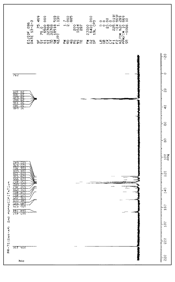
得られた樹脂の13C−NMRスペクトル(装置:ブルカー・バイオスピン社製AC300P、溶媒:アセトンD6、濃度:10質量%)を図1に示す。この13C−NMRスペクトルには165ppmにエステルのカルボニル炭素を示すピークの存在が認められた。また、原料のビスフェノールAノボラック樹脂の13C−NMRスペクトルでは存在が認められた水酸基結合炭素のピーク(152ppm)は確認されなかった。以上のことから、得られた生成物が目的としたアリールエステル付加ビスフェノールAノボラック樹脂(BPANov−AR)であることが確認できた。
【0084】
[ガラス転移温度の測定]
得られた樹脂(BPANov−AR)のガラス転移温度(Tg)をTAインスツルメンツ社製TMA2940を用いて昇温温度10℃/分、引張モードで測定した。結果を表1に示す。
【0085】
【表1】
[両面銅張積層板の作製]
実施例1により得られたBPANov−AR55gに対し、ビフェニルアラルキル型エポキシ樹脂(NC−3000H、日本化薬株式会社製、エポキシ当量:294g/eq、商品名)80g及びジメチルアミノピリジン1gをメチルエチルケトン60gに溶解し、絶縁樹脂組成物ワニスを得た。次いで、このワニスをポリエチレンテレフタレート製シート上に乾燥後の厚みが50μmになるように調整して塗布した。そして、塗布したワニスを150℃で7分間乾燥させた後、解して未硬化の絶縁樹脂層粉を作製した。
【0087】
続いて、1mm厚の四フッ化エチレン樹脂板をスペーサに用い、両側に低粗化銅箔(F0−WS18、古河サーキットフォイル株式会社製、Rz:1.4μm、商品名)の接着処理面を重ね、ステンレス製の鏡板を用いて、温度170℃、成形圧力3MPaで1時間積層成形を行うことにより、実施例1にかかる両面銅箔張積層板を得た。
【0088】
[銅箔引き剥がし強さの測定]
接着性の評価方法として、得られた両面銅張積層板上の1cm幅の銅箔を、5cm/分の速度で引き剥がすことによって銅箔引き剥がし強さを測定した。結果を表1に示す。
【0089】
[比誘電率の測定]
得られた両面銅張積層板の1GHzにおける比誘電率をトリプレート構造直線線路共振法により測定した。結果を表1に示す。
【0090】
[誘電正接の測定]
得られた両面銅張積層板の1GHzにおける誘電正接をトリプレート構造直線線路共振法により測定した。結果を表1に示す。
【0091】
(実施例2)
ビスフェノールAノボラック樹脂に代えて、サリチルアルデヒドフェノールノボラック樹脂(YL−6065、ジャパンエポキシレジン株式会社製、フェノール性水酸基当量117g/eq、商品名)を用いた以外は、合成例1と同様にして合成を行い、実施例2の樹脂を得た。
【0092】
得られた樹脂の13C−NMRスペクトル(装置:ブルカー・バイオスピン社社製AC300P、溶媒:アセトンD6、濃度:10質量%)を図2に示す。13C−NMRスペクトルには165ppmにエステルのカルボニル炭素を示すピークの存在が確認された。また、原料のサリチルアルデヒドフェノールノボラック樹脂には存在した水酸基結合炭素のピーク(152ppm)は認められなかった。以上のことから、得られた生成物が目的としたアリールエステル付加サリチルアルデヒドフェノールノボラック樹脂(SAN−AR)であることが確認できた。
【0093】
得られた樹脂(SAN−AR)のガラス転移温度を実施例1の樹脂と同様にして測定した。結果を表1に示す。
【0094】
また、BPANov−ARに代えて、実施例2で製造したSAN−ARを用いた以外は、実施例1にかかるものと同様にして両面銅張積層板を作製した。得られた両面銅張積層板の銅箔引き剥がし強さ、比誘電率及び誘電正接を実施例1にかかる両面銅張積層板と同様の方法により測定した。結果を表1に示す。
【0095】
(比較例1)
比較例1の樹脂としてビスフェノールAノボラック樹脂(VH−4170、大日本インキ化学工業株式会社製、フェノール性水酸基当量:117g/eq、商品名)を用いた。この樹脂のガラス転移温度を実施例1と同様にして測定した。結果を表1に示す。
【0096】
また、BPANov−ARに代えて、上述したビスフェノールAノボラック樹脂を用いた以外は、実施例1と同様にして両面銅張積層板を作製した。得られた両面銅張積層板の銅箔引き剥がし強さ、比誘電率及び誘電正接を実施例1にかかる両面銅張積層板と同様の方法により測定した。結果を表1に示す。
【0097】
(比較例2)
比較例2の樹脂としてサリチルアルデヒドフェノールノボラック樹脂(YL−6065、ジャパンエポキシレジン株式会社製、フェノール性水酸基当量:117g/eq、商品名)を用いた。この樹脂のガラス転移温度を実施例1と同様にして測定した。結果を表1に示す。
【0098】
また、SAN−ARに代えて、上述したサリチルアルデヒドフェノールノボラック樹脂を用いた以外は、実施例2と同様にして両面銅張積層板を作製した。得られた両面銅張積層板の銅箔引き剥がし強さ、比誘電率及び誘電正接を実施例1にかかる両面銅張積層板と同様の方法により測定した。結果を表1に示す。
【0099】
【発明の効果】
以上説明したように、本発明によれば、粗化の程度の低い導体箔に対しても十分強力に接着して導体張積層板を形成可能な絶縁樹脂組成物を提供することができる。また、本発明によれば、そのような絶縁樹脂組成物を用いたプリプレグ、樹脂付導体箔、導体張積層板及び多層配線板並びに多層配線板の製造方法を提供することが可能となる。
【図面の簡単な説明】
【図1】実施例1の樹脂の13C−NMRスペクトルである。
【図2】実施例2の樹脂の13C−NMRスペクトルである。[0001]
TECHNICAL FIELD OF THE INVENTION
The present invention relates to an insulating resin composition, a prepreg using the same, a resin-coated conductor foil, a conductor-clad laminate, a multilayer wiring board, and a method for manufacturing a multilayer wiring board.
[0002]
[Prior art]
2. Description of the Related Art Conventionally, a laminated board used as a substrate of a printed wiring board is obtained by laminating a predetermined number of insulating layers such as a prepreg layer using a resin having electric insulation as a matrix, and integrating them by heat and pressure. When a conductor circuit is formed by a subtractive method, usually, a conductor-clad laminate obtained by further laminating a conductor foil such as a metal foil (copper foil) on the surface of the above-mentioned laminate and heating and press-bonding the printed circuit is printed wiring. Used as a board substrate.
[0003]
Regarding the adhesion of the conductor foil to the insulator layer, usually, the surface of the conductor foil is roughened to enhance the adhesion using an anchor effect (for example, see Patent Document 1 and Non-Patent Document 1). ).
[0004]
[Patent Document 1]
JP-A-4-211941
[Non-patent document 1]
Electronic Materials Editing Department, "High Density Printed Wiring Board Technology", Industrial Research Committee, May 20, 1986, p149-157
[0005]
[Problems to be solved by the invention]
However, the present inventors have studied in detail the conventional method for bonding a conductive foil described in Patent Document 1 described above. When it was attempted to remove a part of the conductor foil, it was found that there was a high possibility that the conductor foil of the portion to be removed remained.
[0006]
That is, since the surface of the conductor foil is roughened, it is difficult for the etchant to penetrate into the recesses on the surface of the conductor foil. It has been found that it is necessary to perform etching. Remaining portions of the conductor foil to be removed may cause a short circuit, which is not preferable.
[0007]
Furthermore, it is necessary to suppress the electrical resistance of the conductor foil due to the so-called skin effect in order to realize a higher frequency of a signal accompanying a higher processing speed of an electronic device. Here, the "skin effect" means that as the frequency of a signal flowing through a conductor increases, the interference of the lines of magnetic force generated in the center of the conductor increases, so that the current hardly flows in the center of the conductor, but the vicinity of the conductor surface It means that the current flowing through increases. However, it is generally considered that when the surface of the conductor foil is roughened, the electric resistance increases in the vicinity of the surface, and it tends to be difficult for the current to flow. Will be prevented.
[0008]
On the other hand, with the recent increase in the density of wiring in a printed wiring board, or with the increase in the number of terminals of an element mounted on the wiring board and the narrowing of the terminal width, the conductor foil is easily peeled off from the laminate. There is a tendency to improve this.
[0009]
Therefore, the present invention has been made in view of the above circumstances, and provides an insulating resin composition capable of forming a conductor-clad laminate by bonding sufficiently strongly to a conductor foil having a low degree of roughness. With the goal.
[0010]
Another object of the present invention is to provide a prepreg, a resin-coated conductor foil, a conductor-clad laminate, a multilayer wiring board, and a method for producing a multilayer wiring board using the insulating resin composition of the present invention.
[0011]
[Means for Solving the Problems]
The present inventors have conducted intensive studies to achieve the above object, and as a result, a specific repeating unit of the compound contained in the insulating resin composition has an insulating layer and a conductive foil obtained from the insulating resin composition. Have been found to have an effect of improving the adhesiveness with the present invention, and have completed the present invention.
[0012]
That is, the insulating resin composition of the present invention is a compound obtained by reacting a compound having two or more phenolic hydroxyl groups in a molecule with an aromatic carboxylic acid or an aromatic carboxylic acid halide, and has an R-COO group. It is characterized by containing a compound having two or more, an epoxy resin having two or more epoxy groups in a molecule, and an epoxy resin curing accelerator. Here, R represents a monovalent organic group having an aromatic ring.
[0013]
The above compound acts as a curing agent for the epoxy resin by reacting (ring-opening insertion reaction) with the epoxy group of the epoxy resin contained in the insulating resin composition. The epoxy resin curing accelerator contained in the insulating resin composition is used to accelerate the above reaction.
[0014]
The insulating resin composition of the present invention containing such a compound is cured by heating or the like, and exhibits high adhesion to a conductor foil having a low degree of roughening.
[0015]
Further, the insulating resin composition of the present invention containing such a compound can provide an insulator having a sufficiently low relative dielectric constant as compared with a conventional one, and therefore, the insulating resin composition is printed using such an insulating resin composition. When a wiring board is manufactured, an electronic circuit having a high signal propagation speed and excellent electric characteristics can be formed.
[0016]
When the compound is a compound represented by the following general formula (1) or (2), the insulating resin composition of the present invention can form an electronic circuit having more excellent adhesiveness and more excellent electrical characteristics. .
[0017]
Embedded image
[0018]
In the insulator composition of the present invention, X is preferably a monovalent organic group containing an aromatic ring, or Y is preferably a methylene group or a hydroxyphenylmethylene group. Thereby, the adhesive force between the insulator layer obtained from the insulator composition and the conductor foil can be further increased.
[0019]
Further, the insulating resin composition is obtained by adding a compound represented by the general formula (1) or (2) to a compound having a phenolic hydroxyl group and an aldehyde which may be substituted with a ketone or a hydroxyphenyl group. When the compound obtained by reacting an aromatic carboxylic acid or an aromatic carboxylic acid halide with a resin obtained by condensation, it is possible to further improve the adhesiveness. Further, thereby, excellent electrical characteristics as an insulator can be imparted to the insulator layer.
[0020]
In the insulating resin composition of the present invention, the compound having two or more R-COO groups preferably has three or more R-COO groups. Thereby, the adhesiveness between the insulator layer obtained from the insulating resin composition and the conductor foil can be further enhanced.
[0021]
Further, it is preferable that R in the R-COO group is a phenyl group. By having such a chemical species, the insulating resin composition can be manufactured relatively inexpensively, so that it is particularly useful industrially.
[0022]
Further, the insulating resin composition preferably contains dimethylaminopyridine as an epoxy resin curing accelerator. By using such a compound, the insulating resin composition exhibits excellent curability, and thus the insulating layer obtained therefrom can have good adhesiveness and heat resistance.
[0023]
Further, a prepreg of the present invention is characterized in that a base material is impregnated with the above-described insulating resin composition.
[0024]
The conductive foil with resin of the present invention is characterized by comprising a conductive foil and an insulating resin composition layer containing the insulating resin composition formed on the conductive foil.
[0025]
Furthermore, the conductor-clad laminate of the present invention is provided with a conductor foil on a cured product of the above-described prepreg. Alternatively, the conductor-clad laminate of the present invention obtains a laminate by laminating the above-described conductive foil with resin such that the insulating resin composition layer is in contact with the cured product of the prepreg or the prepreg, and then heats the laminate. Then, the insulating resin composition layer and / or the prepreg may be cured.
[0026]
Further, the multilayer wiring board of the present invention is characterized in that, in a multilayer wiring board comprising alternately insulating layers and conductor layers on which circuit patterns are formed, the insulating layer is a cured product of the above-described insulating resin composition. And
[0027]
Furthermore, another multilayer wiring board of the present invention is characterized in that, in a multilayer wiring board comprising alternately insulating layers and conductor layers on which circuit patterns are formed, the insulating layer is a cured product of the above-described prepreg. I do.
[0028]
Since each of the above electronic components uses the insulating resin composition of the present invention, a sufficient insulating force between the insulator layer and the conductor layer can be obtained even if the conductor surface provided therein is relatively smooth. As a result, it is possible to form a fine circuit.
[0029]
The method for producing a multilayer wiring board according to the present invention includes the steps of: providing the conductive foil with resin on the conductive layer of an inner wiring board including an insulating layer and a conductive layer on which a circuit pattern is formed; an insulating resin composition layer of the conductive foil; A laminating step of laminating so as to be in contact with the conductor layer, curing the insulating resin composition layer, a curing step of obtaining a laminated substrate having a conductor foil on the surface, and partially removing the conductor foil of the laminated substrate And a patterning step of forming a circuit pattern on the surface.
[0030]
In the method for manufacturing a multilayer wiring board, a wiring board on which a circuit pattern obtained in the patterning step is formed can be used as an inner layer wiring board in the laminating step.
[0031]
BEST MODE FOR CARRYING OUT THE INVENTION
Hereinafter, preferred embodiments of the present invention will be described in detail.
[0032]
The insulating resin composition according to the present invention is a compound obtained by reacting a compound having two or more phenolic hydroxyl groups in a molecule with an aromatic carboxylic acid or an aromatic carboxylic acid halide, wherein the R-COO group has 2 It contains a compound having the above, an epoxy resin having two or more epoxy groups in a molecule, and an epoxy resin curing accelerator.
[0033]
(Compound having two or more R-COO groups)
The compound having two or more R-COO groups is obtained by reacting a compound having two or more phenolic hydroxyl groups in a molecule with an aromatic carboxylic acid or an aromatic carboxylic acid halide. Here, R represents a monovalent organic group having an aromatic ring.
[0034]
Examples of the compound having two or more phenolic hydroxyl groups in the molecule include a monocyclic phenol compound having two phenolic hydroxyl groups such as hydroquinone and catechol, a bifunctional phenol compound such as bisphenol A, bisphenol F or bisphenol S, and phenol. A polyfunctional phenol resin such as a novolak resin, a cresol novolak resin, a bisphenol A novolak resin, a salicylaldehyde phenol novolak resin, a biphenylaralkyl type phenol resin, or naphthalene diol is exemplified.
[0035]
The aromatic carboxylic acid or aromatic carboxylic acid halide can be employed without any particular limitation as long as it has a monovalent organic group containing an aromatic ring in the molecule. Among these, from the viewpoint of production cost, it is preferable to use a benzoic acid halide such as benzoic acid or benzoic acid chloride in which the monovalent organic group R containing an aromatic ring is a phenyl group.
[0036]
When using an aromatic carboxylic acid as a reaction between a compound having two or more phenolic hydroxyl groups in the molecule and an aromatic carboxylic acid or an aromatic carboxylic acid halide, for example, the compound at a temperature of 250 ° C. or more When an aromatic carboxylic acid halide is used, for example, a reaction between the compound and an aromatic carboxylic acid halide in the presence of an amine can be mentioned.
[0037]
Examples of the compound having two or more R-COO groups obtained by this reaction include both a compound in which an aromatic ring is directly bonded to a carbonyl carbon and a compound in which a side chain of an aromatic ring is bonded to a carbonyl carbon. A compound having two or more R-COO groups in one aromatic ring, a compound having one or more R-COO groups in each of two or more aromatic rings, and the like are given.
[0038]
The insulating resin composition of the present invention preferably contains a compound represented by the following general formula (1) or (2) among these compounds from the viewpoint of adhesiveness and the like.
[0039]
Embedded image
[0040]
The compound represented by the general formula (1) or (2) can be obtained by various production methods, and the production method is not particularly limited. For example, first, a compound having a phenolic hydroxyl group and an aldehyde optionally substituted with a ketone or a hydroxylphenyl group may be subjected to addition condensation.
[0041]
Examples of the compound having a phenolic hydroxyl group include a phenol, a monocyclic phenol compound having one phenolic hydroxyl group such as cresol or ethylphenol, and a monocyclic phenol compound having two phenolic hydroxyl groups such as hydroquinone or catechol. Examples include phenol compounds, bifunctional phenol compounds such as bisphenol A, bisphenol F and bisphenol S, and naphthalene diol.
[0042]
Examples of the aldehyde that may be substituted with a hydroxyphenyl group include formaldehyde, acetaldehyde, propylene aldehyde, and the like, and aldehydes substituted with those hydroxyphenyl groups. Of these, formaldehyde or salicylaldehyde is preferred from the viewpoint of the adhesiveness of the finally obtained insulator layer.
[0043]
Further, examples of the ketone include acetone, ethyl methyl ketone, isopropyl methyl ketone, acetophenone and the like.
[0044]
Subsequently, for example, the compound represented by the general formula (1) or (2) is obtained by reacting the condensation compound obtained by the above addition condensation reaction with an aromatic carboxylic acid or an aromatic carboxylic acid halide. Can be As this reaction, the same as the above-described reaction between the condensation compound and the aromatic carboxylic acid or the like can be mentioned.
[0045]
The condensation compound used in this reaction is obtained by the above addition condensation reaction, has two or more phenolic hydroxyl groups in the molecule, and furthermore has a hydrogen atom or a monovalent organic group X and a divalent organic group. A compound having a group Y or a compound having two or more phenolic hydroxyl groups in a molecule and having an n-valent organic group Z. Specifically, for example, bifunctional phenols such as bisphenol A, bisphenol F, bisphenol S, or phenol novolak resin, cresol novolak resin, bisphenol A novolak resin, salicylaldehyde phenol novolak resin, biphenyl aralkyl type phenol resin, etc. Polyfunctional phenol resins and the like can be mentioned.
[0046]
Among these, from the viewpoint of improving the adhesiveness of the insulator layer, it is obtained by using bisphenol A as the compound having a phenolic hydroxyl group and using formaldehyde or salicylaldehyde as the aldehyde which may be substituted with a hydroxyphenyl group. Bisphenol A novolak resins or salicylaldehyde phenol novolak resins are particularly preferred.
[0047]
The compound having two or more R-COO groups obtained in this manner makes it possible to finally obtain an insulating layer having a strong adhesive force by including the compound in an insulating resin composition. Therefore, for example, while the surface roughness of a copper foil conventionally used for a copper-clad laminate had a ten-point average roughness of 6 μm or more, when the insulating resin composition of the present invention was adopted, the copper Even when the ten-point average roughness of the foil is 2 μm or less, a sufficiently strong adhesive force between the copper foil and the insulating layer can be secured. As a result, it becomes possible to manufacture a fine circuit having a wiring width of about 20 μm, which has been difficult to realize using a conventional copper foil having a relatively rough surface.
[0048]
(Epoxy resin)
The epoxy resin used in the present invention is not particularly limited as long as it is a compound having two or more epoxy groups in a molecule. Therefore, examples of the epoxy resin include bisphenol type epoxy resin, novolak type epoxy resin, glycidyl ester type epoxy resin, glycidylamine type epoxy resin, aliphatic chain epoxy resin and epoxidized polybutadiene. Among these, the adhesiveness with the conductor foil is particularly good, and from the viewpoint of improving the filling property and heat resistance of the inner layer circuit, when a bisphenol-type epoxy resin or a novolak-type epoxy resin is used as the epoxy resin according to the present invention. preferable.
[0049]
Examples of the bisphenol epoxy resin include a bisphenol A epoxy resin, a bisphenol F epoxy resin, a bisphenol S epoxy resin, and the like. Examples of the novolak epoxy resin include a phenol novolak epoxy resin, a bisphenol A novolak epoxy resin, a cresol novolak epoxy resin, and a salicylaldehyde phenol novolak epoxy resin.
[0050]
These resins can be used alone or in combination of two or more. The molecular weight of these resins is not particularly limited.
[0051]
(Epoxy resin curing accelerator)
The epoxy resin curing accelerator is not particularly limited as long as it is a compound that promotes the formation of a reaction product (cured product) of the epoxy resin described above. Specific examples include imidazoles, organic phosphorus compounds, tertiary amines, and quaternary ammonium salts.
[0052]
Examples of imidazoles include imidazole, 1-methylimidazole, 2-methylimidazole, 4-methylimidazole, 2-ethyl-4-methylimidazole, 2-phenylimidazole, 2-undecylimidazole, 1-benzyl-2-methylimidazole , 4-phenylimidazole, benzimidazole or 1-cyanoethyl-2-methylimidazole. Examples of the organic phosphorus compound include triphenylphosphine. Furthermore, examples of the tertiary amine include triethylamine, tributylamine, pyridine and dimethylaminopyridine. Examples of the quaternary ammonium salt include tetrabutylammonium acetate and tetrabutylammonium hydrogen sulfate.
[0053]
Among these, it is preferable to use dimethylaminopyridine as an epoxy resin curing accelerator since the epoxy resin has good curability and can exhibit excellent adhesiveness and heat resistance.
[0054]
Next, the mixing ratio of each of the above components contained in the insulating resin composition of the present invention will be described.
[0055]
The compounding amount of the compound having two or more R-COO groups is preferably 20 to 300 parts by mass with respect to 100 parts by mass of the epoxy resin. If the compounding amount of the compound is less than 20 parts by mass relative to 100 parts by mass of the epoxy resin, the curability of the epoxy resin tends not to be ensured. On the other hand, if the compounding amount of the compound exceeds 300 parts by mass with respect to 100 parts by mass of the epoxy resin, the compound is present in an excessive amount and tends to act as a plasticizer for the resin obtained from the insulating resin composition. is there.
[0056]
Further, the R-COO group equivalent in the compound is preferably adjusted so as to be 0.8 to 1.2 in a ratio (epoxy equivalent / R-COO group equivalent) to the epoxy equivalent in the epoxy resin. . Thereby, the resin obtained by curing the insulating resin composition can have heat resistance and good adhesiveness to the conductive foil.
[0057]
The compounding amount of the epoxy resin curing accelerator is preferably 0.01 to 10 parts by mass with respect to 100 parts by mass of the epoxy resin. If the amount of the epoxy resin curing accelerator is less than 0.01 part by mass, the epoxy resin tends not to be sufficiently cured, and if it exceeds 10 parts by mass, the heat resistance of the obtained resin tends to decrease.
[0058]
The insulating resin composition of the present invention may further contain various additives as needed, and may further contain, for example, an inorganic filler. Examples of the inorganic filler include alumina, aluminum hydroxide, magnesium hydroxide, clay, talc, antimony trioxide, zinc oxide, fused silica, glass powder, quartz powder, and shirasu balloon. These additives can be used alone or in combination of two or more.
[0059]
The insulating resin composition of the present invention can also contain a solvent, if necessary, in order to mix each component and make it in a coatable state, that is, to form a varnish. The solvent can be used without any particular limitation as long as it is capable of dissolving the above-mentioned components and does not affect the adhesiveness of the obtained resin. Specific examples include various alcohols, acetone, toluene, xylene, ketone, amide, ether, pyrrolidone, and the like. Among them, from the viewpoints of solubility and boiling point of the epoxy resin, ethanol, isopropyl alcohol, acetone, methyl ethyl ketone, methyl butyl ketone, toluene, xylene, ethyl acetate, N, N-dimethylformamide, N, N-dimethylacetamide And ethylene glycol monomethyl ether or N-methylpyrrolidone. These solvents can be used alone or in combination of two or more.
[0060]
The insulating resin composition of the present invention can be used for a prepreg for multilayering, a conductor foil with resin, a conductor-clad laminate, a multilayer wiring board by a build-up method, and the like.
[0061]
When the insulating resin composition is used for a prepreg for multilayering, the prepreg is formed by impregnating the base material with the insulating resin composition. Examples of the substrate include glass fibers made of E glass, D glass, S glass, Q glass, or the like, organic fibers made of polyimide, polyester, tetrafluoroethylene, or the like, and fibers obtained by mixing these. These fibers can be used as a base material in the form of, for example, a woven fabric, a nonwoven fabric, a roving, a chopped strand mat or a surfacing mat. The thickness of the base material can be, for example, about 0.03 to 0.5 mm, and from the viewpoint of improving heat resistance, moisture resistance, or workability, the silane cup has a thickness that does not affect the adhesiveness. It is preferable to use one that has been surface-treated with a ring agent or the like or one that has been mechanically opened.
[0062]
Examples of the method of impregnating the base material with the insulating resin composition include, for example, a method of dipping the base material in a resin liquid such as a wet method or a dry method, or a method of coating the base material with the insulating resin composition. . The amount of the insulating resin composition impregnated in the base material is preferably 20 to 90% by mass, more preferably 30 to 80% by mass, based on the total mass of the dried prepreg. Then, by heating the substrate impregnated with the thermosetting resin composition at 100 to 200 ° C. for 1 to 30 minutes to remove the solvent, a prepreg in which the thermosetting resin composition is in a semi-cured state is obtained. be able to.
[0063]
Since the prepreg thus obtained has excellent adhesiveness to the conductor molded product, it can be provided in an electronic material having peeling resistance without roughening its surface or the surface of the conductor molded product. Can be used.
[0064]
When the insulating resin composition is used for the resin-coated conductor foil, it is provided with a conductor foil and an insulating resin composition layer containing the insulating resin composition of the present invention. Such a resin-coated conductor foil is formed, for example, by applying a varnish (primer) containing the above-described insulating resin composition on the conductor foil, and then heating the resin foil at a temperature of 100 to 200 ° C. for 1 to 30 minutes to remove the solvent. Can be obtained.
[0065]
Examples of the conductor foil include a copper foil, an aluminum foil, and a nickel foil. When producing a resin-coated conductor foil, a conductor foil having a thickness of usually 10 to 50 μm is used, and a resin-coated conductor foil in which a resin is adhered to a conductor foil having a thickness of 1 to 10 μm is prepared by the following method. be able to. That is, as the conductor foil on which the insulating resin composition layer is formed, a conductor foil composed of two layers, a support conductor foil that can be removed by etching or peeling and an ultrathin conductor foil, is prepared. Then, an insulating resin composition layer is formed on the ultrathin conductor foil of the conductor foil, and the supporting conductor foil is removed by etching or peeling. The thickness of the insulating resin composition layer in the resin-coated conductor foil is preferably 10 to 150 μm as a thickness after heating, and the amount of the residual solvent in the layer is about 0.2 to 10%. Is appropriate.
[0066]
When the insulating resin composition is used for a conductor-clad laminate, the conductor-clad laminate is provided with a normal conductor foil on a cured product of a prepreg formed using the insulating resin composition of the present invention as described above. There may be. Alternatively, the above-described conductive foil with a resin of the present invention is laminated so that the insulating resin composition layer is in contact with the cured product of the prepreg or the prepreg to obtain a laminate, and then the laminate is heated to form the insulating resin composition. It may be obtained by curing a material layer and / or a prepreg.
[0067]
The manufacturing method is as follows. First, after laminating, for example, 1 to 20 prepregs by a known method, the prepreg is cured by heating and pressing as necessary. The molding is usually performed using a multi-stage press, a multi-stage vacuum press, a continuous molding or an autoclave molding machine, and the heating and pressing are performed at a temperature of 100 to 250 ° C. and a pressure of 2 to 100 kg / cm. 2 And 0.1 to 5 hours. Then, one side or both sides of the laminated prepreg are brought into close contact with the surface of the conductor foil when the conductor foil is not provided with a resin, or the resin when the conductor foil is a conductor foil provided with a resin, and the whole is heated and / or heated. By pressing, a conductor-clad laminate can be obtained.
[0068]
When the insulating resin composition is used for a multilayer wiring board, it can be used, for example, as follows. That is, first, a wiring board having a conductor layer on which a circuit pattern is formed on one or both sides as an inner layer wiring board, on the conductor layer of such an inner layer wiring board, from the insulating resin composition of the present invention as an insulator layer After the insulating resin composition layer is formed, it is cured to obtain a wiring board for an inner layer and a wiring board with an insulator layer having an insulator layer.
[0069]
Next, drilling or drilling is performed on the obtained wiring board with an insulator layer. Next, the resin residue generated during drilling is removed. In addition, by using the insulating resin composition of the present invention, the adhesive force between the insulator layer and the conductor layer can be increased, so that the step of roughening the surface is not necessarily required, If it is desired to further increase the temperature, sandblasting, plasma treatment, chemical treatment with an oxidizing agent such as permanganate or dichromate, or the like is performed.
[0070]
Further, a via hole is formed by electroless copper plating, metal evaporation, sputtering, ion plating, or the like, and a circuit pattern is formed on the insulating resin composition layer by a known method such as plating or etching, and the circuit pattern is formed on the surface. A laminate having the formed conductor layer is obtained. Then, by using the obtained laminate as a wiring board for an inner layer and repeating the steps from the formation of the insulating resin composition layer to the formation of the circuit pattern, a multilayer wiring board can be obtained. A multilayer wiring board provided with a cured prepreg can be manufactured by replacing the insulating resin composition in the above method with a prepreg.
[0071]
The formation of the insulating resin composition layer on the wiring board is performed by applying the insulating resin composition of the present invention on the conductor layer of the wiring board and then heating and curing the composition. The insulating resin composition (or prepreg) can be cured by heating at a temperature of 120 ° C. or more for 15 minutes or more, preferably at a temperature of 170 to 220 ° C. for 60 to 150 minutes.
[0072]
In addition, examples of the substrate used for the wiring board for the inner layer include a glass epoxy substrate, a metal substrate, a polyester substrate, a BT resin substrate, and a thermosetting PPE substrate.
[0073]
In addition, the production of the multilayer wiring board can also be performed by using the above-described conductive foil with resin. Such a method is described below. That is, first, a wiring board having a conductor layer on which a circuit pattern is formed on one or both sides is used as an inner wiring board, and the above-described conductive foil with resin is placed on the conductor layer of the inner wiring board by heating and / or pressing conditions. A laminating step of laminating or pressing underneath to perform lamination so that the resin in the resin-coated conductor foil is in contact with the resin foil is performed. Next, the resin is cured by heating the resin portion, and a curing step of obtaining a laminated substrate having a conductor foil on the surface is performed.
[0074]
Further, a patterning step of partially removing the conductor foil surface of the obtained laminated substrate by a known method such as etching to form a circuit pattern on the surface is performed.
[0075]
Then, using a wiring board having a circuit pattern formed on its surface as an inner wiring board, and performing the above-described three steps including the laminating step, the curing step, and the patterning step once or twice or more to obtain a multilayer wiring board Can be.
[0076]
After the curing step, via holes or the like may be formed in the laminated substrate. Drilling of the laminated board is necessary to form via holes.If the conductive foil on the laminated board is thin, drilling or laser can be used to make the hole directly.If the conductive foil is thick, the conformal mask method is used. Alternatively, after forming a window hole by the large window method, the hole can be formed by drilling with a drill or a laser. Here, it is preferable to roughen the surface of the conductive foil on the laminated substrate by sandblasting, plasma treatment, chemical treatment with an oxidizing agent such as permanganate or dichromate, or the like. Such roughening may be performed before drilling, or may be performed after drilling.
[0077]
After drilling, if a resin residue remains on the surface of the conductive foil or through hole, the resin residue is removed, and a via hole can be formed by electroless copper plating, metal evaporation, sputtering, ion plating, or the like.
[0078]
In each of the electronic components thus obtained, since the resin and the conductor provided therein are inherently excellent in adhesion, the surface of the conductor foil is sufficiently roughened in order to use the anchor effect. There is no need to provide a finer circuit.
[0079]
Further, since the resin has excellent electrical characteristics such as relative permittivity, the above-mentioned electronic components using the resin are effectively provided in, for example, electronic devices which need to increase the processing speed.
[0080]
【Example】
Hereinafter, the present invention will be described in more detail with reference to Examples, but the present invention is not limited to these Examples.
[0081]
(Example 1)
First, bisphenol A novolak resin (VH-4170, manufactured by Dainippon Ink and Chemicals, Inc., phenolic hydroxyl equivalent: 117 g /) was placed in a 2 L four-necked flask equipped with a thermometer, a cooling pipe, a nitrogen introduction pipe, and a stirring rod. eq, trade name) 250 g and cyclohexanone 700 g were added and dissolved by stirring under a nitrogen stream, then refluxed at 150 ° C., and water was removed using a Dean-Stark fractionator. Next, 400 g of triethylamine was added, and the inside of the reaction system was cooled to 10 ° C. or lower by an ice bath, and 400 g of benzoic acid chloride was added dropwise over 2 hours while taking care that the reaction system did not exceed 10 ° C. After the completion of the dropwise addition, the mixture was further reacted by stirring at room temperature for 2 hours.
[0082]
After completion of the reaction, triethylamine hydrochloride was removed by suction filtration, and the obtained filtrate was precipitated in methanol. Then, the precipitate was dried under reduced pressure at 120 ° C. for 1 hour to obtain a crude product. Subsequently, the crude product was dissolved in 200 g of acetone, the insoluble components were removed by filtration under reduced pressure, and the product was reprecipitated in methanol to obtain a product. Thereafter, the product was dried under reduced pressure at 120 ° C. for 6 hours to obtain the resin of Example 1.
[0083]
Of the obtained resin Thirteen FIG. 1 shows a C-NMR spectrum (apparatus: AC300P manufactured by Bruker BioSpin, solvent: acetone D6, concentration: 10% by mass). this Thirteen In the C-NMR spectrum, the presence of a peak indicating the carbonyl carbon of the ester at 165 ppm was recognized. In addition, the raw material bisphenol A novolak resin Thirteen In the C-NMR spectrum, the peak of the hydroxyl-bonded carbon (152 ppm) whose presence was recognized was not confirmed. From the above, it was confirmed that the obtained product was the target aryl ester-added bisphenol A novolak resin (BPANAv-AR).
[0084]
[Measurement of glass transition temperature]
The glass transition temperature (Tg) of the obtained resin (BPANov-AR) was measured in a tensile mode using a TMA2940 manufactured by TA Instruments at a temperature elevation temperature of 10 ° C./min. Table 1 shows the results.
[0085]
[Table 1]
[Production of double-sided copper-clad laminate]
80 g of a biphenylaralkyl-type epoxy resin (NC-3000H, manufactured by Nippon Kayaku Co., Ltd., epoxy equivalent: 294 g / eq, trade name) and 1 g of dimethylaminopyridine were added to 60 g of methyl ethyl ketone with respect to 55 g of the BPA Nov-AR obtained in Example 1. It melt | dissolved and the insulating resin composition varnish was obtained. Next, the varnish was applied to a sheet made of polyethylene terephthalate such that the thickness after drying was adjusted to 50 μm. Then, the applied varnish was dried at 150 ° C. for 7 minutes, and then opened to prepare an uncured insulating resin layer powder.
[0087]
Subsequently, a 1 mm-thick tetrafluoroethylene resin plate was used as a spacer, and an adhesive-treated surface of low-roughened copper foil (F0-WS18, made by Furukawa Circuit Foil Co., Ltd., Rz: 1.4 μm, trade name) was provided on both sides. The two-sided copper foil-clad laminate according to Example 1 was obtained by laminating and performing lamination molding for 1 hour at a temperature of 170 ° C. and a molding pressure of 3 MPa using a stainless steel end plate.
[0088]
[Measurement of copper foil peeling strength]
As a method of evaluating adhesiveness, the copper foil peeling strength was measured by peeling a 1 cm wide copper foil on the obtained double-sided copper-clad laminate at a speed of 5 cm / min. Table 1 shows the results.
[0089]
[Measurement of relative permittivity]
The relative permittivity at 1 GHz of the obtained double-sided copper-clad laminate was measured by a triplate structure straight line resonance method. Table 1 shows the results.
[0090]
[Measurement of dielectric loss tangent]
The dielectric loss tangent at 1 GHz of the obtained double-sided copper-clad laminate was measured by a triplate structure straight line resonance method. Table 1 shows the results.
[0091]
(Example 2)
Synthesized in the same manner as in Synthesis Example 1 except that salicylaldehyde phenol novolak resin (YL-6065, manufactured by Japan Epoxy Resin Co., Ltd., phenolic hydroxyl equivalent: 117 g / eq, trade name) was used instead of bisphenol A novolak resin. Was carried out to obtain a resin of Example 2.
[0092]
Of the obtained resin Thirteen FIG. 2 shows a C-NMR spectrum (apparatus: AC300P manufactured by Bruker Biospin, solvent: acetone D6, concentration: 10% by mass). Thirteen In the C-NMR spectrum, the presence of a peak indicating the carbonyl carbon of the ester at 165 ppm was confirmed. In addition, the peak of the hydroxyl-bonded carbon (152 ppm) present in the salicylaldehyde phenol novolak resin as the raw material was not observed. From the above, it was confirmed that the obtained product was the desired aryl ester-added salicylaldehyde phenol novolak resin (SAN-AR).
[0093]
The glass transition temperature of the obtained resin (SAN-AR) was measured in the same manner as in the resin of Example 1. Table 1 shows the results.
[0094]
Further, a double-sided copper-clad laminate was produced in the same manner as in Example 1, except that the SAN-AR manufactured in Example 2 was used instead of BPANov-AR. The copper foil peel strength, relative dielectric constant and dielectric loss tangent of the obtained double-sided copper-clad laminate were measured in the same manner as for the double-sided copper-clad laminate according to Example 1. Table 1 shows the results.
[0095]
(Comparative Example 1)
As the resin of Comparative Example 1, a bisphenol A novolak resin (VH-4170, manufactured by Dainippon Ink and Chemicals, Inc., phenolic hydroxyl equivalent: 117 g / eq, trade name) was used. The glass transition temperature of this resin was measured in the same manner as in Example 1. Table 1 shows the results.
[0096]
Further, a double-sided copper-clad laminate was produced in the same manner as in Example 1, except that the above-mentioned bisphenol A novolak resin was used instead of BPANov-AR. The copper foil peel strength, relative dielectric constant and dielectric loss tangent of the obtained double-sided copper-clad laminate were measured in the same manner as for the double-sided copper-clad laminate according to Example 1. Table 1 shows the results.
[0097]
(Comparative Example 2)
Salicylaldehyde phenol novolak resin (YL-6065, manufactured by Japan Epoxy Resin Co., Ltd., phenolic hydroxyl equivalent: 117 g / eq, trade name) was used as the resin of Comparative Example 2. The glass transition temperature of this resin was measured in the same manner as in Example 1. Table 1 shows the results.
[0098]
Further, a double-sided copper-clad laminate was produced in the same manner as in Example 2 except that the above-mentioned salicylaldehyde phenol novolak resin was used instead of the SAN-AR. The copper foil peel strength, relative dielectric constant and dielectric loss tangent of the obtained double-sided copper-clad laminate were measured in the same manner as for the double-sided copper-clad laminate according to Example 1. Table 1 shows the results.
[0099]
【The invention's effect】
As described above, according to the present invention, it is possible to provide an insulating resin composition capable of forming a conductor-clad laminate by bonding sufficiently strongly to a conductor foil having a low degree of roughening. Further, according to the present invention, it is possible to provide a prepreg, a resin-coated conductor foil, a conductor-clad laminate, a multilayer wiring board, and a method for manufacturing a multilayer wiring board using such an insulating resin composition.
[Brief description of the drawings]
FIG. 1 shows the resin of Example 1 Thirteen It is a C-NMR spectrum.
FIG. 2 shows the resin of Example 2; Thirteen It is a C-NMR spectrum.
Claims (15)
分子内に2以上のエポキシ基を有するエポキシ樹脂と、
エポキシ樹脂硬化促進剤と、
を含有することを特徴とする絶縁樹脂組成物。A compound obtained by reacting a compound having two or more phenolic hydroxyl groups in a molecule with an aromatic carboxylic acid or an aromatic carboxylic acid halide, wherein an R-COO group (R is a monovalent having an aromatic ring) A compound having two or more).
An epoxy resin having two or more epoxy groups in a molecule,
An epoxy resin curing accelerator,
An insulating resin composition comprising:
前記絶縁体層が請求項1〜7のいずれか一項に記載の絶縁樹脂組成物の硬化物であることを特徴とする多層配線板。In a multilayer wiring board comprising alternately insulating layers and conductor layers on which circuit patterns are formed,
A multilayer wiring board, wherein the insulator layer is a cured product of the insulating resin composition according to any one of claims 1 to 7.
前記絶縁体層が請求項8記載のプリプレグの硬化物であることを特徴とする多層配線板。In a multilayer wiring board comprising alternately insulating layers and conductor layers on which circuit patterns are formed,
A multilayer wiring board, wherein the insulator layer is a cured product of the prepreg according to claim 8.
前記絶縁樹脂組成物層を硬化させ、表面に前記導体箔を備える積層基板を得る硬化工程と、
前記積層基板の前記導体箔を部分的に除去して、表面に回路パターンを形成させるパターニング工程と、を含むことを特徴とする多層配線板の製造方法。The resin-coated conductor foil according to claim 9, wherein the insulating resin composition layer of the conductor foil is formed on the conductor layer of the inner layer wiring board including an insulator layer and a conductor layer on which a circuit pattern is formed. A laminating step of laminating so as to touch,
Curing the insulating resin composition layer, a curing step to obtain a laminated substrate provided with the conductive foil on the surface,
A patterning step of partially removing the conductive foil of the laminated substrate to form a circuit pattern on a surface thereof.
Priority Applications (1)
| Application Number | Priority Date | Filing Date | Title |
|---|---|---|---|
| JP2003161189A JP2004359867A (en) | 2003-06-05 | 2003-06-05 | Insulation resin composition, prepreg produced by using the same, conductor foil with resin, conductor-clad laminated board and method for producing multilayer circuit board |
Applications Claiming Priority (1)
| Application Number | Priority Date | Filing Date | Title |
|---|---|---|---|
| JP2003161189A JP2004359867A (en) | 2003-06-05 | 2003-06-05 | Insulation resin composition, prepreg produced by using the same, conductor foil with resin, conductor-clad laminated board and method for producing multilayer circuit board |
Publications (1)
| Publication Number | Publication Date |
|---|---|
| JP2004359867A true JP2004359867A (en) | 2004-12-24 |
Family
ID=34053722
Family Applications (1)
| Application Number | Title | Priority Date | Filing Date |
|---|---|---|---|
| JP2003161189A Pending JP2004359867A (en) | 2003-06-05 | 2003-06-05 | Insulation resin composition, prepreg produced by using the same, conductor foil with resin, conductor-clad laminated board and method for producing multilayer circuit board |
Country Status (1)
| Country | Link |
|---|---|
| JP (1) | JP2004359867A (en) |
Cited By (6)
| Publication number | Priority date | Publication date | Assignee | Title |
|---|---|---|---|---|
| JP2010113241A (en) * | 2008-11-07 | 2010-05-20 | Taiyo Ink Mfg Ltd | Photosetting resin composition, dry film and cured product of the same, and printed wiring board using them |
| JP2010237576A (en) * | 2009-03-31 | 2010-10-21 | Taiyo Ink Mfg Ltd | Curable resin composition |
| JP2010266745A (en) * | 2009-05-15 | 2010-11-25 | Taiyo Ink Mfg Ltd | Curable resin composition |
| JP2014089960A (en) * | 2013-11-07 | 2014-05-15 | Ajinomoto Co Inc | Method for manufacturing multilayer printed wiring board |
| CN112457631A (en) * | 2019-09-06 | 2021-03-09 | 广东生益科技股份有限公司 | Active ester resin, preparation method thereof, thermosetting resin composition containing active ester resin, prepreg and laminated film |
| JPWO2023167049A1 (en) * | 2022-03-03 | 2023-09-07 |
-
2003
- 2003-06-05 JP JP2003161189A patent/JP2004359867A/en active Pending
Cited By (8)
| Publication number | Priority date | Publication date | Assignee | Title |
|---|---|---|---|---|
| JP2010113241A (en) * | 2008-11-07 | 2010-05-20 | Taiyo Ink Mfg Ltd | Photosetting resin composition, dry film and cured product of the same, and printed wiring board using them |
| JP2010237576A (en) * | 2009-03-31 | 2010-10-21 | Taiyo Ink Mfg Ltd | Curable resin composition |
| JP2010266745A (en) * | 2009-05-15 | 2010-11-25 | Taiyo Ink Mfg Ltd | Curable resin composition |
| JP2014089960A (en) * | 2013-11-07 | 2014-05-15 | Ajinomoto Co Inc | Method for manufacturing multilayer printed wiring board |
| CN112457631A (en) * | 2019-09-06 | 2021-03-09 | 广东生益科技股份有限公司 | Active ester resin, preparation method thereof, thermosetting resin composition containing active ester resin, prepreg and laminated film |
| CN112457631B (en) * | 2019-09-06 | 2023-04-07 | 广东生益科技股份有限公司 | Active ester resin, preparation method thereof, thermosetting resin composition containing active ester resin, prepreg and laminated film |
| JPWO2023167049A1 (en) * | 2022-03-03 | 2023-09-07 | ||
| WO2023167049A1 (en) * | 2022-03-03 | 2023-09-07 | 日鉄ケミカル&マテリアル株式会社 | Epoxy resin composition, reinforcing fiber-containing epoxy resin composition, prepreg, fiber reinforced plastic employing same, and thermoplastic epoxy resin |
Similar Documents
| Publication | Publication Date | Title |
|---|---|---|
| JP6572983B2 (en) | Epoxy resin composition | |
| TWI756552B (en) | Thermosetting epoxy resin composition, adhesive film for insulating layer formation, prepreg for insulating layer formation, insulator for printed wiring board, multilayer printed wiring board, and semiconductor device | |
| JP5950005B2 (en) | Resin composition | |
| JP5573869B2 (en) | Resin composition for interlayer insulation layer of multilayer printed wiring board | |
| KR102128231B1 (en) | Curable resin composition | |
| JP7385344B2 (en) | Thermosetting resin composition and multilayer substrate | |
| KR101314382B1 (en) | Resin composition for printed circuit board | |
| TW202214731A (en) | Curable resin, curable resin composition, cured product, varnish, prepreg, and circuit board | |
| JP5011641B2 (en) | Thermosetting resin composition, adhesive film using the same, and multilayer printed wiring board | |
| JP2020029494A (en) | Resin composition for insulating layer, sheet-like laminated material, multilayer printed wiring board, and semiconductor device | |
| KR20080108469A (en) | Epoxy resin composition | |
| JP2009001787A (en) | Polyphenylene ether resin composition and electronic member | |
| KR102126657B1 (en) | Curable resin composition | |
| WO2003099952A1 (en) | Adhesive film and prepreg | |
| JP2004359867A (en) | Insulation resin composition, prepreg produced by using the same, conductor foil with resin, conductor-clad laminated board and method for producing multilayer circuit board | |
| JP4830748B2 (en) | Flame retardant epoxy resin composition, resin film, prepreg and multilayer printed wiring board | |
| JPWO2020045112A1 (en) | Laminates, metal foil-clad laminates, patterned metal foil laminates, laminates with build-up structures, printed wiring boards, multilayer coreless substrates, and methods of manufacturing them. | |
| JP2003127313A (en) | Adhesive film and prepreg | |
| KR20230049098A (en) | Copper foil with a resin layer and a laminate using the same | |
| JP7352799B2 (en) | Resin compositions, prepregs, resin-coated films, resin-coated metal foils, metal-clad laminates, and printed wiring boards | |
| JP2004259899A (en) | Printed circuit board, resin composition therefor, and multilayer printed circuit board | |
| JP4600359B2 (en) | Epoxy resin composition, resin film, prepreg, and multilayer printed wiring board | |
| JP2009051938A (en) | Epoxy resin composition, cured product thereof, resin composition for buildup film, novel epoxy resin, and production method thereof | |
| KR102884159B1 (en) | Insulating resin layer attachment substrate, and laminate using the same and method for manufacturing laminate | |
| JP2007051226A (en) | Resin composition with low dielectric constant |