JP2004303529A - Sealing member for organic electroluminescence element and organic electroluminescence element - Google Patents
Sealing member for organic electroluminescence element and organic electroluminescence element Download PDFInfo
- Publication number
- JP2004303529A JP2004303529A JP2003093831A JP2003093831A JP2004303529A JP 2004303529 A JP2004303529 A JP 2004303529A JP 2003093831 A JP2003093831 A JP 2003093831A JP 2003093831 A JP2003093831 A JP 2003093831A JP 2004303529 A JP2004303529 A JP 2004303529A
- Authority
- JP
- Japan
- Prior art keywords
- organic
- sealing member
- metal foil
- layer
- light
- Prior art date
- Legal status (The legal status is an assumption and is not a legal conclusion. Google has not performed a legal analysis and makes no representation as to the accuracy of the status listed.)
- Granted
Links
Images


Classifications
-
- H—ELECTRICITY
- H10—SEMICONDUCTOR DEVICES; ELECTRIC SOLID-STATE DEVICES NOT OTHERWISE PROVIDED FOR
- H10K—ORGANIC ELECTRIC SOLID-STATE DEVICES
- H10K50/00—Organic light-emitting devices
- H10K50/80—Constructional details
- H10K50/84—Passivation; Containers; Encapsulations
- H10K50/842—Containers
- H10K50/8423—Metallic sealing arrangements
Landscapes
- Physics & Mathematics (AREA)
- Optics & Photonics (AREA)
- Electroluminescent Light Sources (AREA)
Abstract
【課題】本発明の課題とするところは、薄型・軽量で、大量生産を行っても性能にばらつきのない有機EL素子およびそれを得るための封止部材とを提供することにある。
【解決手段】少なくとも支持基材、剥離樹脂層、金属箔からなる封止部材の、金属箔が所定の複数形状にパターニングされ、剥離樹脂層と金属箔の界面が剥離することを特徴とする有機EL素子用封止部材を用いて有機EL素子を封止する。透明電極と対向電極及びその間に挟持された層が透光性基材上に複数個設けられ、かつ、透光性基材に第二のアライメントマークが設けられている有機EL発光素子を、前記封止部材の金属箔を接着層を介して転写・積層すると、薄い金属箔をしわ等にならずに封止に用いることが可能になり、かつ、一定張力をかけながら封止するために、同一基材上の個々の素子の封止端面が均一となり、従って各素子の耐湿性能の揃った有機EL素子を提供することができる。
【選択図】図3An object of the present invention is to provide an organic EL element which is thin and lightweight, and whose performance does not vary even when mass-produced, and a sealing member for obtaining the same.
An organic material, wherein a metal foil of a sealing member comprising at least a support substrate, a release resin layer, and a metal foil is patterned into a predetermined plurality of shapes, and an interface between the release resin layer and the metal foil is peeled off. The organic EL element is sealed using an EL element sealing member. An organic EL light-emitting element in which a plurality of transparent electrodes and a counter electrode and a layer sandwiched therebetween are provided on a light-transmitting substrate, and the second alignment mark is provided on the light-transmitting substrate. When the metal foil of the sealing member is transferred and laminated via an adhesive layer, it becomes possible to use the thin metal foil for sealing without wrinkling, etc., and to seal while applying a constant tension, The sealing end faces of the individual elements on the same base material are uniform, and therefore, it is possible to provide an organic EL element having uniform humidity resistance of each element.
[Selection diagram] FIG.
Description
【0001】
【発明の属する技術分野】
本発明は、情報表示端末などのディスプレイや面発光光源として幅広い用途が期待される有機エレクトロルミネッセンス素子(以下、有機EL素子と表記する)用の封止部材及びその封止部材に適した有機EL発光素子並びにそれらによって作成された有機EL素子に関するものである。
【0002】
【従来の技術】
有機EL素子は、広視野角、応答速度が速い、低消費電力などの利点から、ブラウン管や液晶ディスプレイに変わるフラットパネルディスプレイとして期待されている。
【0003】
有機EL素子は、透明陽極と陰極との間に有機発光媒体層を挟持した構造であり、両電極間に電流を流すことにより有機発光媒体層で発光が生じるものである。
【0004】
有機発光媒体層は多層構造をとることが多く、その典型的な例としては、正孔注入層として銅フタロシアニン、正孔輸送層としてN,N’−ジ(1−ナフチル)−N,N’−ジフェニル−1,1’−ビフェニル−4,4’−ジアミン、蛍光体層としてトリス(8−キノリノール)アルミニウムなどが積層された低分子型有機EL素子や、正孔輸送層としてポリ(3,4−エチレンジオキシチオフェン)とポリスチレンスルホン酸との混合物、蛍光体層としてポリフルオレンなどが積層された高分子型EL素子がある。
【0005】
有機EL素子の持つ大きな問題の一つは、発光媒体層や陰極層が大気暴露状態で放置されると、大気中の水分や酸素などにより劣化することである。具体例の一つとして、ダークスポットと呼ばれる非発光領域が発生し、時間の経過と共に拡大するといった現象がある。
【0006】
この問題を解決する手段が特許文献1や特許文献2などで開示されている。これらは、陽極となる透明電極を形成したガラス基板上に発光媒体層、対向電極を真空下で連続成膜し、金属製やガラス製の封止缶により乾燥窒素雰囲気下でEL素子を被覆封止する方法である。
【0007】
しかし、ガラスや金属製の封止缶を用いる為、有機EL素子を薄型・軽量化するのに限界があった。また、製造工程においては、気密ケース内部に乾燥剤を封入する工程、気密ケースに光硬化性樹脂を塗布する工程、透光性基板と気密ケースを貼り合せる工程、光硬化性樹脂を硬化させる工程があるため、生産性・製造コストの面で問題があった。
【0008】
これに対し、近年、プラスチックフィルムやガラス上に、高分子発光媒体層をスピンコート法やグラビア印刷法、インクジェット法などの湿式法で成膜し、金属箔などのバリア性の高いフィルムを用いて封止することにより、耐湿性に優れた薄型・軽量な有機EL素子が、特許文献3や特許文献4などで提案されている。
【0009】
しかし、金属箔を撓ませずに保持し、接着層中に気泡が残留しないように、接着層の膜厚が全面均一になるように金属箔を貼り合せることが困難であるといった問題があった。特に、厚みが50μm以下である金属箔を用いて、しわ等の発生を起こさずに封止することは困難であった。さらに、金属箔の可撓性ゆえに、封止後の有機EL素子の封止面を平滑に保つことが難しく、従って封止したEL素子側面から侵入する水分の量も側面毎に異なり、安定した耐湿性能を有する有機EL素子の生産は難しかった。
【0010】
【特許文献1】
特開平5−182759号公報
【特許文献2】
特開平5−36475号公報
【特許文献3】
特開2001−307871号公報
【特許文献4】
特開2002−50470号公報
【0011】
【発明が解決しようとする課題】
本発明は上記の問題点を解決するためになされたものであり、その課題とするところは、特に耐湿性能の安定性に優れて長期にわたり劣化を抑制することができ、生産時の歩留まりが良く、薄型・軽量の有機EL素子を提供することのできる封止部材及びおよび有機EL素子を提供することである。
【0012】
【課題を解決するための手段】
本発明は上記課題を解決するためなされたものであり、請求項1に係る第1の発明は、少なくとも支持基材、剥離樹脂層、金属箔からなる封止部材の、金属箔が所定の形状にパターニングされ、剥離樹脂層と金属箔の界面が剥離し、有機エレクトロルミネッセンス発光素子を封止するために用いられることを特徴とする有機エレクトロルミネッセンス素子用封止部材である。
【0013】
請求項2に係る第2の発明は、前記所定の形状にパターニングされた金属箔を有する封止部材は、1枚の前記支持基材に、複数個設けられていることを特徴とする請求項1記載の有機エレクトロルミネッセンス素子用封止部材である。
【0014】
請求項3に係る第3の発明は、前記支持基材上に、第一のアライメントマークを設けたことを特徴とする請求項1または2記載の有機エレクトロルミネッセンス素子用封止部材である。
【0015】
請求項4に係る第4の発明は、前記有機エレクトロルミネッセンス発光素子は、透光性基材上に少なくとも透明電極、有機発光媒体層、対向電極を有し、かつ、透明電極と対向電極及びその間に挟持された層が透光性基材上に複数個設けられ、かつ、透光性基材に第二のアライメントマークが設けられていることを特徴とする請求項1記載の有機エレクトロルミネッセンス素子用封止部材である。
【0016】
請求項5に係る第5の発明は、請求項1から3のいずれかに記載の有機エレクトロルミネッセンス素子用封止部材の所定の形状にパターニングされた金属箔が、接着層を介して、請求項4に記載の有機エレクトロルミネッセンス発光素子上に転写・積層されていることを特徴とする有機エレクトロルミネッセンス素子である。
【0017】
【発明の実施の形態】
以下、本発明の封止部材及びこの部材を用いて封止する有機EL発光素子並びに有機EL素子の製造の一例を、図1〜図4に基づいて説明する。
【0018】
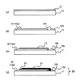
まず始めに、封止部材10の製造方法について図1を用いて説明する。まず、封止部材の基材1の一方の面上に、第一のアライメントマーク2を作製した後に(図1(a))、剥離樹脂層3を形成する(図1(b))。次に、剥離樹脂層3上に金属箔4を積層した後に(図1(c))、金属箔4をパターニングすることにより、封止部材10が完成する(図1(d))。
【0019】
封止部材の基材1の材料としては、ポリプロピレン、ポリエーテルサルフォン、ポリカーボネート、シクロオレフィンポリマー、ポリアリレート、ポリアミド、ポリメチルメタクリレート、ポリエチレンテレフタレート、ポリエチレンナフタレート等のプラスチックフィルムを用いることができる。製造効率を上げるためには、封止部材の基材1をロール状の可撓性基材とし、複数の金属箔をその上に積層し、有機EL発光素子へ連続巻き取りによって転写することが好ましく、この場合は封止部材の基材としては連続巻き取り・転写に耐える引張り強度・温度特性を有する材料が好ましい。
【0020】
本発明においては、金属箔を有機EL発光素子に転写する際の位置合わせのために封止部材及び有機EL発光素子の透光性基材のそれぞれにアライメントマークを設けることが望ましい。本明細書中では、封止部材側に設けられたものを第一のアライメントマーク、有機EL発光素子側に設けられたものを第二のアライメントマークとする。
【0021】
第一のアライメントマーク2は、図1において、剥離樹脂層3と同じ面に積層したが、他方の面に形成しても良い。(封止部材の基材側から見てアライメントマークが確認できればよい。)形成方法としては、グラビア印刷法やスクリーン印刷法やインクジェット法などの印刷法を用いてインキ層を形成しても良く、着色性のフォトレジスト材料などをフォトリソ法を用いてパターン形成しても良く、ITO膜やクロム膜などの蒸着膜をパターン形成したものを用いても良い。また、レーザー等で直接封止部材の基材に印をつけ、これを第一のアライメントマークとすることも可能である。
【0022】
剥離樹脂層3の材料としては、エポキシ系樹脂、アクリル系樹脂、シリコーン樹脂、ウレタン樹脂などからなる光硬化型接着性樹脂、熱硬化型接着性樹脂、2液硬化型接着性樹脂や、ポリエチレン、ポリプロピレンなどの酸変性物からなる熱可塑性接着性樹脂などを単層もしくは積層して用いることができる。特に、ロール状の封止部材の基材1へ金属箔4を積層する場合には、短時間で接着し、接着後もロール巻取りが容易であることが好ましい。例えば、封止部材の基材1上に、剥離樹脂層3としてポリエチレンやポリプロピレンなどの酸変性物からなる熱可塑性接着性樹脂をウレタン系接着剤を用いてドライラミネートすることが好ましい。また、封止部材の基材1と剥離樹脂層3との接着強度が、剥離樹脂層3と金属箔4界面の接着強度よりも高くなるよう、封止部材の基材1表面と剥離樹脂層3表面を、予め、コロナ放電処理、プラズマ処理、UVオゾン処理などの表面処理を施すことが好ましく、さらには、酸化珪素、窒化珪素、酸窒化珪素などの無機絶縁薄膜や、クロム、チタンなどの金属薄膜などの薄膜を挿入しても良い。また、必要に応じて、有機チタン系、イソシアネート系、ポリエチレンイミン系などの下塗り材を用いて接着強度を高めることがより好ましい。剥離樹脂層3の形成方法としては、材料に応じて、ロールコート、スピンコート、スクリーン印刷法、スプレーコートなどのコーティング法、印刷法を用いて塗布しても良く、ドライフィルムを用いて熱圧着法やドライラミネート法を用いて積層することもできる。
【0023】
金属箔4の材料としては、アルミニウム、銅、ニッケルなどの金属材料や、ステンレス、アルミニウム合金などの合金材料を用いることができるが、加工性やコストの面でアルミニウムがより好ましい。
また、金属箔4と剥離樹脂層3が剥離しやすくなるよう、必要に応じて、ポリエステルアクリレート、ポリエステルアリルアクリルアミドなどの長鎖アルキル基含有ポリマーや、フェニルメチルシロキサンとジメチルシロキサンのコポリマーなどのシリコーン系ポリマーや、ポリ(1,1−シヒドロパ−フロロヘキシルメタクリレート)、ポリ(N−エチル、N−パーフロロオクタンスルホアミドエチルメタクリレート)などのパーフロロ系ポリマーなどを(剥離樹脂層と金属箔との間に)使用してもよい。また、金属箔4のパターニング方法としては、レーザー等による機械的エッチングで行うこともできるが、一度に大面積を処理できるフォトリソグラフィー法及びウェットエッチング法を用いることが好ましい。
【0024】
封止部材の基材1上に剥離樹脂層を介して複数形状にパターニングされた金属箔が積層されていると、この封止部材10により複数の有機EL発光素子を同時に、あるいは連続で封止することができ、かつ、このとき複数の有機EL素子にかかる圧力・張力・温度等の物理的要因が一定になるため、均一な品質の有機EL発光素子を製造することができる。
さらには、本発明の封止部材はロール状、すなわち一連続の巻き取り可能な可撓性基材上に剥離樹脂層、複数形状にパターニングされた金属箔が設けられていることが好ましい。封止部材がロール状であることによって、図4に示すように有機EL発光素子20の連続封止が可能となる。また、一定の張力をかけた封止部材から均一な圧力・張力・温度により、パターニングされた金属箔を連続して有機EL発光素子に転写するため、金属箔が薄くてもしわやムラにならず、ピンホールのできない限度であればどんなに薄い金属箔でも封止することが可能である。また金属箔のみをラミネートする場合と異なり、薄い金属箔に必要以上の張力がかかることもない。具体的には15〜100μmの範囲の厚みの金属箔であればよく、素子の薄型化のために50μm以下を好ましく用いることができ、ピンホールがおこらない程度である30μmが上限として最も好ましい。
【0025】
さらに、金属箔のみを直接有機EL発光素子に貼り付ける封止では、金属箔自身の可撓性のために、封止面が傾いたり歪んだりして平滑にならず、従って封止した有機EL素子の側面の開口面積も側面毎に異なるため、安定した防湿性能を有する有機EL素子の製造は難しかったが、金属箔を封止部材の一部とし、これをアライメントマークにより位置合わせして転写するという方法で封止を行うと、開口部の厚みが一定である安定した品質の有機EL素子を一度に生産することができる。さらに、封止をロール状の封止部材を用いた連続巻き取り工程で行うことにより、生産効率を高めることができる。
【0026】
次に、封止部材で封止する有機EL発光素子20の作製方法について図2を用いて説明する。
本明細書中では、区別のために、封止前である、透光性基材11上に少なくとも透明電極12、有機発光媒体層13、対向電極14を積層した素子を有機EL発光素子20とし、これに接着層21を介して金属箔4で封止を行ったものを有機EL素子と呼ぶこととする(例えば図2、図3参照)。
【0027】
まず初めに、透光性基材11の一方の面に、スパッタリング法等により陽極として働く透明電極12を形成した(図1(a))後に、フォトリソグラフィー法及びウエットエッチング法を用いて、透明電極12をパターニングすることにより、陽極取りだし電極12aを兼ねた透明電極12と、陰極取りだし電極12bと、第二のアライメントマーク12cを作製した(図2(b))。
【0028】
ここで、本実施の形態において、透光性基材11の材料としては、透光性と絶縁性を有する基板であれば如何なる基材も使用することができる。例えば、ガラスや石英や、ポリプロピレン、ポリエーテルサルフォン、ポリカーボネート、シクロオレフィンポリマー、ポリアリレート、ポリアミド、ポリメチルメタクリレート、ポリエチレンテレフタレート、ポリエチレンナフタレート等のプラスチックフィルムやシート、または、これらプラスチックフィルムやシートに酸化珪素、酸化アルミニウム、窒化珪素金属酸化物や、酸化珪素、酸化アルミニウム、酸化クロム、酸化マグネシウム等の金属酸化物、弗化アルミニウム、弗化マグネシウム等の金属弗化物、窒化珪素、窒化アルミニウム、窒化クロムなどの金属窒化物、酸窒化珪素などの金属酸窒化物、アルミニウム、銅、ニッケル、ステンレスなどの金属材料、アクリル樹脂やエポキシ樹脂、シリコーン樹脂、ポリエステル樹脂などの高分子樹脂膜を、透光性に支障が無い範囲で、単層もしくは積層して用いることができる。特に、金属酸化物などの無機薄膜が透明性とバリア性において好ましいが、ピンホールなどの膜欠陥を生じやすく、たとえ厚膜化しても下地の膜欠陥を反映してしまうため、無機薄膜の単独膜ではなく、高分子樹脂膜などとの積層膜を用いることがより好ましい。また、これらの基材には、必要に応じて、あらかじめ加熱処理を行うことにより、基材内部や表面に吸着した水分を極力低減することがより好ましい。また、透光性基材11と透明電極12との密着性を向上させるために、透光性基材11表面は、超音波洗浄処理、コロナ放電処理、プラズマ処理、UVオゾン処理などの表面処理を施すことが好ましく、さらには透光性に支障が無い範囲内で、酸化珪素、窒化珪素、酸窒化珪素などの無機絶縁薄膜や、クロム、チタンなどの金属薄膜などの薄膜を挿入することがより好ましい。
【0029】
透光性基材11に設ける第二のアライメントマークは、、既述の封止部材の基材に設けた第一のアライメントマークと同様、インキ等で形成してもよいし、レーザー等で直接書き込むこともできるが、ここでは簡便であるため透明電極12のパターニングと同時に形成した例を示す。
【0030】
透明電極12の材料としては、ITO(インジウムスズ複合酸化物)やインジウム亜鉛複合酸化物、亜鉛アルミニウム複合酸化物などの金属複合酸化物や、金、白金などの金属材料や、これら金属酸化物や金属材料の微粒子をエポキシ樹脂やアクリル樹脂などに分散した微粒子分散膜を、単層もしくは積層して使用することができる。また、透明電極の配線抵抗を低くするために、銅やアルミニウムなどの金属材料を補助電極として、透明電極に併設してもよい。透明電極12の形成方法としては、材料に応じて、抵抗加熱蒸着法、電子ビーム蒸着法、反応性蒸着法、イオンプレーティング法、スパッタリング法などの乾式成膜法や、グラビア印刷法、スクリーン印刷法などの湿式成膜法などを用いることができる。透明電極12のパターニング方法としては、材料や成膜方法に応じて、マスク蒸着法、フォトリソグラフィー法、ウェットエッチング法、ドライエッチング法などの既存のパターニング法を用いることができる。
【0031】
次に、有機発光媒体層13及び対向電極14を順次成膜する(図1(c)、(d))。
【0032】
本発明における有機発光媒体層13としては、蛍光物質を含む単層膜、あるいは多層膜で形成することができる。多層膜で形成する場合の有機発光媒体層の構成例は正孔注入輸送層、電子輸送性発光層または正孔輸送性発光層、電子輸送層からなる2層構成や正孔注入輸送層、発光層、電子輸送層からなる3層構成等がある。さらにより多層で形成することも可能であり、各層を基板上に順に成膜する。
【0033】
正孔注入輸送材料の例としては、銅フタロシアニン、テトラ(t−ブチル)銅フタロシアニン等の金属フタロシアニン類及び無金属フタロシアニン類、キナクリドン化合物、1,1−ビス(4−ジ−p−トリルアミノフェニル)シクロヘキサン、N,N’−ジフェニル−N,N’−ビス(3−メチルフェニル)−1,1’−ビフェニル−4,4’−ジアミン、N,N’−ジ(1−ナフチル)−N,N’−ジフェニル−1,1’−ビフェニル−4,4’−ジアミン等の芳香族アミン系低分子正孔注入輸送材料やポリチオフェン、ポリアニリン等の高分子正孔輸送材料、ポリチオフェンオリゴマー材料、その他既存の正孔輸送材料の中から選ぶことができる。
【0034】
発光材料の例としては、9,10−ジアリールアントラセン誘導体、ピレン、コロネン、ペリレン、ルブレン、1,1,4,4−テトラフェニルブタジエン、トリス(8−キノリノラート)アルミニウム錯体、トリス(4−メチル−8−キノリノラート)アルミニウム錯体、ビス(8−キノリノラート)亜鉛錯体、トリス(4−メチル−5−トリフルオロメチル−8−キノリノラート)アルミニウム錯体、トリス(4−メチル−5−シアノ−8−キノリノラート)アルミニウム錯体、ビス(2−メチル−5−トリフルオロメチル−8−キノリノラート)[4−(4−シアノフェニル)フェノラート]アルミニウム錯体、ビス(2−メチル−5−シアノ−8−キノリノラート)[4−(4−シアノフェニル)フェノラート]アルミニウム錯体、トリス(8−キノリノラート)スカンジウム錯体、ビス〔8−(パラ−トシル)アミノキノリン〕亜鉛錯体及びカドミウム錯体、1,2,3,4−テトラフェニルシクロペンタジエン、ペンタフェニルシクロペンタジエン、ポリ−2,5−ジヘプチルオキシ−パラ−フェニレンビニレン、クマリン系蛍光体、ペリレン系蛍光体、ピラン系蛍光体、アンスロン系蛍光体、ポルフィリン系蛍光体、キナクリドン系蛍光体、N,N’−ジアルキル置換キナクリドン系蛍光体、ナフタルイミド系蛍光体、N,N’−ジアリール置換ピロロピロール系蛍光体等の低分子材料や、ポリフルオレン、ポリパラフェニレンビニレン、ポリチオフェンなどの高分子材料、その他既存の発光材料を用いることができる。
【0035】
有機電子輸送材料の例としては、2−(4−ビフィニルイル)−5−(4−t−ブチルフェニル)−1,3,4−オキサジアゾール、2,5−ビス(1−ナフチル)−1,3,4−オキサジアゾール、および浜田らの合成したオキサジアゾール誘導体(日本化学会誌、1540頁、1991年)やビス(10−ヒドロキシベンゾ[h]キノリノラート)ベリリウム錯体、特開平7−90260号で述べられているトリアゾール化合物等が挙げられる。
【0036】
有機発光媒体層13の形成方法は、材料に応じて、真空蒸着法や、スピンコート、スプレーコート、フレキソ、グラビア、マイクログラビア、凹版オフセットなどのコーティング法、印刷法を用いることができる。ダイコート法によれば、ロール状の透光性基材を用いて連続で製膜することができ、かつ透明電極等の透光性基材上に生じた凹凸を埋めてむらのない有機発光媒体層を得ることができるため好ましいが、一つの透光性基材上に多面付けで有機EL素子を製造するため、この場合はふき取りやフォトリソなどのパターニング工程が必要となる。有機発光媒体層の膜厚は、単層または積層により形成する場合においても1000nm以下であり、好ましくは50〜150nmである。
【0037】
陰極として働く対向電極14の材料としては、電子注入効率の高い物質を用いる。具体的にはMg、Al、Yb等の金属単体を用いたり、発光媒体と接する界面にLiや酸化Li、LiF等の化合物を1nm程度挟んで、安定性・導電性の高いAlやCuを積層して用いる。または電子注入効率と安定性を両立させるため、仕事関数が低いLi、Mg、Ca、Sr、La、Ce、Er、Eu、Sc、Y、Yb等の金属1種以上と、安定なAg、Al、Cu等の金属元素との合金系が用いられる。具体的にはMgAg、AlLi、CuLi等の合金が使用できる。対向電極14の形成方法としては、材料に応じて、抵抗加熱蒸着法、電子ビーム蒸着法、反応性蒸着法、イオンプレーティング法、スパッタリング法を用いることができる。陰極の厚さは、10nm〜1000nm程度が望ましい。また、対向電極14上には、必要に応じて、酸化珪素、酸化アルミニウム、窒化珪素金属酸化物や、酸化珪素、酸化アルミニウム、酸化クロム、酸化マグネシウム等の金属酸化物、弗化アルミニウム、弗化マグネシウム等の金属弗化物、窒化珪素、窒化アルミニウム、窒化クロムなどの金属窒化物、酸窒化珪素などの金属酸窒化物、アルミニウム、銅、ニッケル、ステンレスなどの金属材料、アクリル樹脂やエポキシ樹脂、シリコーン樹脂、ポリエステル樹脂などの高分子樹脂膜などを、単層もしくは複数層積層して用いることができる。
【0038】
次に、長期にわたり、外部の水分や酸素から有機EL素子20を遮断するために、接着層21を介して、封止部材10を積層する(図3(a))。この時、第一のアライメントマーク2と第二のアライメントマーク12cとを合わせるように積層することにより、透光性基材11上の有機発光媒体層13や対向電極14と封止部材の基材1上の金属箔4の位置合わせを正確に行うことができる。接着層21を硬化させた後に、剥離樹脂層3と金属箔4との界面を剥離し(図3(b))、有機EL素子から封止部材の基材1と剥離樹脂層3を取り除くことにより、透光性基材11上に多数個作製された有機EL発光素子20について一つ一つをパターニングされた金属箔4により同時(図3(b))に、あるいは連続して(図4)封止することができる。
【0039】
接着層21の材料としては、エポキシ系樹脂、アクリル系樹脂、シリコーン樹脂などからなる光硬化型接着性樹脂、熱硬化型接着性樹脂、2液硬化型接着性樹脂や、ポリエチレン、ポリプロピレンなどの酸変性物からなる熱可塑性接着性樹脂などを用いることができる。特に、耐湿性、耐水性に優れ、硬化時の収縮が少ないエポキシ系熱硬化型接着性樹脂を用いることが好ましい。接着層21の形成方法としては、材料に応じて、ロールコート、スピンコート、スクリーン印刷法、スプレーコートなどのコーティング法、印刷法を用いることができる。また、金属箔4と接着層21との接着性を向上させるために、予め、金属箔4の表面をアセトンやイソプロピルアルコールなどの有機溶剤や、UVオゾン洗浄、プラズマ洗浄、コロナ洗浄などを用いて表面処理することがより好ましい。また、接着層21内部の含有水分を除去するために、酸化バリウムや酸化カルシウムなどの乾燥剤を加えてもよい。
【0040】
【実施例】
実施の形態に基づいた実施例1及び、比較例1を図1〜図4に従って説明する。
【0041】
<実施例1>
a.封止部材の作成
封止部材の基材1として、ポリエチレンテレフタレートフィルム(幅300mm、厚み188μm)を用い、第一のアライメントマーク2として、フタロシアニン系の色素で着色したインキをスクリーン印刷法を用いてパターン成膜した(図1(a))。次に、封止部材の基材1および第一のアライメントマーク2の表面をコロナ処理した後に、剥離樹脂層3として、ウレタン系接着剤を介して、ポリエチレンの酸変性物からなる熱可塑性接着性樹脂フィルムをドライラミネートした(図1(c))。次に、金属箔4として、アルミニウム箔(厚み50μm)を積層した(図1(d))。次に、フォトリソグラフィー法およびウェットエッチング法を用いて、金属箔4をパターニングし、封止部材10を作製した(図1(d))。
【0042】
b.有機EL発光素子の作成
まず、透光性基材11として、ガラス基材(300mm角、厚み0.7mm)を用い、スパッタリング法で透明電極12としてITO膜を150nm形成した(図2(a))後に、フォトリソグラフィー法及びウェットエッチング法によって、ITO膜をパターンニングし、陽極取りだし電極12aを兼ねた透明電極2と、陰極取りだし電極12bと、第二のアライメントマーク12cを作製した(図2(b))。次に、有機発光媒体層13として、正孔輸送層にポリ(3,4−エチレンジオキシチオフェン)とポリスチレンスルホン酸との混合物(20nm)、蛍光体層にポリ[2−メトキシ−5−(2’−エチル−ヘキシロキシ)−1,4−フェニレン ビニレン](MEHPPV)(100nm)をそれぞれスピンコート法により形成した(図2(c))後に、陰極となる対向電極14として、真空蒸着法によりCa(20nm)とAg(200nm)をこの順に積層形成し(図2(d))、有機EL発光素子20を、透光性基材11上に3行かける3列の計9素子作製した。
【0043】
c.有機EL発光素子の封止
有機EL発光素子20上に接着層21として熱硬化型エポキシ接着剤を積層し、封止部材10上の第一のアライメントマーク2と、透光性基材11上の第二のアライメントマーク12cとの位置を合わせるようにして、封止部材10の金属箔4と有機EL発光素子20の対向電極14とを、接着層21を介して、重ね合わせた(図3(a))後に、接着層21を硬化させ(90℃、1h)、剥離樹脂層3と金属箔4との界面を剥離し、有機EL発光素子から封止部材の基材1と剥離樹脂層3を除去することにより、透光性基材11上に9個作製された有機EL発光素子20を金属箔4によってまとめて封止した(図3(b))。金属箔4により封止された9個の有機EL素子30を1つ1つに切断し、60℃90RH%恒温恒湿層中で2000時間保存した。封止端面である接着層21の露出部から侵入した水分が、対向電極14の周辺部(封止額縁5mm)まで達し、9個の有機EL素子30の陰極端非発光部の距離を測定した結果、500μm±10μmの範囲となった。
【0044】
<比較例1>
実施例1に記載した有機EL発光素子において、金属箔として実施例1と同じアルミニウム箔(厚み50μm)を用い、これのみを直接有機EL発光素子に貼り付けることで、1透光性基材上に1素子が作成されている有機EL素子9個を別々に封止し、60℃90RH%恒温恒湿層中で2000時間保存した。封止時に金属箔がたわんだため封止表面がゆがみ、接着層21の厚みを一定に保持することができず、従って9個の有機EL素子の封止端面の面積にばらつきが生じ、接着層21の露出部から侵入する水分量にもばらつきが生じたため、9個の有機EL素子の陰極端非発光部の距離は、450μm〜650μmの範囲で分布していた。
【0045】
【発明の効果】
以上、本発明によれば、薄い金属箔を用いてもしわになったりたわんだりせずに有機EL素子を封止でき、同じ条件で同時に複数の有機EL発光素子を封止するため、安定した品質の有機EL素子を同時に、あるいは連続して製造できる。さらに封止部材をロール状とし、ロール巻き取り工法によって複数の金属箔を複数の有機EL発光素子に連続して積層するため、生産効率を高めることができる。封止部材及び有機EL発光素子の双方にアライメントマークを設けることによって、正確な位置合わせが可能となり、また転写法によれば、金属箔単独でラミネート等を行う場合と異なり、金属箔に余分な力や不均一な張力がかからないため、薄い金属箔でも封止面を平滑にすることが可能であり、金属箔の可撓性ゆえに発生する封止端面の接着層露出面積を一定にすることができる。従って、有機EL素子の長寿命化及び薄型化、そして製造される有機EL素子の耐湿性能の均一化が可能となり、安定かつ高性能の有機EL素子を提供することができる。
【0046】
【図面の簡単な説明】
【図1】本発明で用いる封止部材の製造方法及び断面構造の一例を説明する図である。
【図2】本発明の有機EL発光素子の製造方法及び断面構造の一例を説明する図である。
【図3】本発明の有機EL素子の製造方法及び断面構造の一例を説明する図である。
【図4】本発明の有機EL素子の製造方法の一例を説明する図である。
【符号の説明】
1 …封止部材の基材
2 …第一のアライメントマーク
3 …剥離樹脂層
4 …金属箔
10 …封止部材
11 …透光性基材
12 …透明電極
12a…陽極取りだし電極
12b…陰極取りだし電極
12c…第二のアライメントマーク
13 …有機発光媒体層
14 …対向電極
20 …有機EL発光素子
21 …接着層
22 …位置合わせライン
30 …封止された有機EL素子[0001]
TECHNICAL FIELD OF THE INVENTION
The present invention relates to a sealing member for an organic electroluminescent element (hereinafter referred to as an organic EL element), which is expected to be widely used as a display such as an information display terminal or a surface emitting light source, and an organic EL suitable for the sealing member. The present invention relates to a light emitting device and an organic EL device formed by using the same.
[0002]
[Prior art]
The organic EL element is expected as a flat panel display replacing a CRT or a liquid crystal display due to advantages such as a wide viewing angle, a high response speed, and low power consumption.
[0003]
The organic EL element has a structure in which an organic light emitting medium layer is sandwiched between a transparent anode and a cathode, and light is generated in the organic light emitting medium layer by passing a current between both electrodes.
[0004]
The organic light emitting medium layer often has a multilayer structure. Typical examples are copper phthalocyanine as a hole injection layer and N, N′-di (1-naphthyl) -N, N ′ as a hole transport layer. -Diphenyl-1,1'-biphenyl-4,4'-diamine, a low-molecular-weight organic EL device in which tris (8-quinolinol) aluminum or the like is laminated as a phosphor layer, or poly (3,4) as a hole transport layer. There is a polymer EL element in which a mixture of 4-ethylenedioxythiophene) and polystyrene sulfonic acid and polyfluorene or the like are laminated as a phosphor layer.
[0005]
One of the major problems of the organic EL element is that when the light emitting medium layer and the cathode layer are left in the state of exposure to the air, the light emitting medium layer and the cathode layer are deteriorated by moisture, oxygen and the like in the air. As a specific example, there is a phenomenon that a non-light-emitting area called a dark spot occurs and expands with the passage of time.
[0006]
Means for solving this problem are disclosed in
[0007]
However, since a sealing can made of glass or metal is used, there is a limit in reducing the thickness and weight of the organic EL element. Further, in the manufacturing process, a step of enclosing a desiccant in the hermetic case, a step of applying a photocurable resin to the hermetic case, a step of bonding the translucent substrate to the hermetic case, and a step of curing the photocurable resin Therefore, there was a problem in terms of productivity and manufacturing cost.
[0008]
On the other hand, in recent years, a polymer light emitting medium layer has been formed on a plastic film or glass by a wet method such as a spin coating method, a gravure printing method, an ink jet method, and a film having a high barrier property such as a metal foil has been used. Thin and lightweight organic EL elements having excellent moisture resistance by sealing are proposed in
[0009]
However, there is a problem that it is difficult to hold the metal foil without bending and to bond the metal foil so that air bubbles do not remain in the adhesive layer so that the film thickness of the adhesive layer is uniform over the entire surface. . In particular, it has been difficult to seal using a metal foil having a thickness of 50 μm or less without causing wrinkles or the like. Furthermore, because of the flexibility of the metal foil, it is difficult to keep the sealing surface of the organic EL element after sealing smooth, and therefore, the amount of moisture entering from the side of the sealed EL element is also different for each side, and is stable. It has been difficult to produce an organic EL device having moisture resistance.
[0010]
[Patent Document 1]
JP-A-5-182759
[Patent Document 2]
JP-A-5-36475
[Patent Document 3]
JP 2001-307871 A
[Patent Document 4]
JP-A-2002-50470
[0011]
[Problems to be solved by the invention]
The present invention has been made in order to solve the above problems, and it is an object of the present invention to be able to suppress deterioration over a long period of time, particularly with excellent stability of moisture resistance performance, and to improve the production yield. Another object of the present invention is to provide a sealing member and an organic EL element which can provide a thin and lightweight organic EL element.
[0012]
[Means for Solving the Problems]
Means for Solving the Problems The present invention has been made to solve the above problems, and a first invention according to
[0013]
A second invention according to
[0014]
A third invention according to a third aspect is the sealing member for an organic electroluminescence element according to the first or second aspect, wherein a first alignment mark is provided on the support base material.
[0015]
A fourth invention according to claim 4, wherein the organic electroluminescent light emitting element has at least a transparent electrode, an organic light emitting medium layer, and a counter electrode on a light-transmitting substrate, and the transparent electrode and the counter electrode and between the transparent electrode and the counter electrode. The organic electroluminescent device according to
[0016]
According to a fifth aspect of the present invention, the metal foil patterned into a predetermined shape of the sealing member for an organic electroluminescent element according to any one of the first to third aspects is provided with an adhesive layer interposed therebetween. 4. An organic electroluminescent device, wherein the organic electroluminescent device is transferred and laminated on the organic electroluminescent light emitting device according to 4.
[0017]
BEST MODE FOR CARRYING OUT THE INVENTION
Hereinafter, an example of the sealing member of the present invention, an organic EL light emitting element sealed using the member, and an example of manufacturing the organic EL element will be described with reference to FIGS.
[0018]
First, a method for manufacturing the sealing
[0019]
As a material of the
[0020]
In the present invention, it is desirable that alignment marks are provided on each of the sealing member and the light-transmissive substrate of the organic EL light emitting element for alignment when transferring the metal foil to the organic EL light emitting element. In this specification, the mark provided on the sealing member side is referred to as a first alignment mark, and the mark provided on the organic EL element is referred to as a second alignment mark.
[0021]
Although the
[0022]
Examples of the material of the
[0023]
As a material of the metal foil 4, a metal material such as aluminum, copper, nickel or the like, or an alloy material such as stainless steel or an aluminum alloy can be used, but aluminum is more preferable in view of workability and cost.
If necessary, a silicone-based polymer such as a long-chain alkyl group-containing polymer such as polyester acrylate or polyester allyl acrylamide, or a copolymer of phenylmethylsiloxane and dimethylsiloxane may be used so that the metal foil 4 and the
[0024]
When a plurality of patterned metal foils are laminated on the
Furthermore, the sealing member of the present invention is preferably provided with a release resin layer and a metal foil patterned in a plurality of shapes on a roll-shaped, that is, a continuous rollable flexible base material. When the sealing member has a roll shape, the organic EL
[0025]
Furthermore, in the encapsulation in which only the metal foil is directly adhered to the organic EL element, the sealing surface is not smooth due to inclination or distortion due to the flexibility of the metal foil itself. Since the opening area of the side surface of the device also differs for each side surface, it was difficult to manufacture an organic EL device having stable moisture-proof performance. However, a metal foil was used as a part of the sealing member, and this was aligned and transferred using an alignment mark. When the sealing is performed by such a method, a stable quality organic EL element having a constant opening thickness can be produced at a time. Furthermore, by performing sealing in a continuous winding step using a roll-shaped sealing member, production efficiency can be increased.
[0026]
Next, a method for manufacturing the organic EL light-emitting
In the present specification, for the sake of distinction, an element in which at least a
[0027]
First, a
[0028]
Here, in this embodiment, as the material of the light-transmitting
[0029]
The second alignment mark provided on the
[0030]
Examples of the material of the
[0031]
Next, an organic light emitting
[0032]
The organic light emitting
[0033]
Examples of the hole injecting and transporting material include metal phthalocyanines such as copper phthalocyanine and tetra (t-butyl) copper phthalocyanine, and metal-free phthalocyanines, quinacridone compounds, 1,1-bis (4-di-p-tolylaminophenyl). ) Cyclohexane, N, N'-diphenyl-N, N'-bis (3-methylphenyl) -1,1'-biphenyl-4,4'-diamine, N, N'-di (1-naphthyl) -N , N'-diphenyl-1,1'-biphenyl-4,4'-diamine and other aromatic amine-based low-molecular-weight hole injection / transport materials, high-molecular-weight hole transport materials such as polythiophene and polyaniline, polythiophene oligomer materials, and others You can choose from existing hole transport materials.
[0034]
Examples of light emitting materials include 9,10-diarylanthracene derivatives, pyrene, coronene, perylene, rubrene, 1,1,4,4-tetraphenylbutadiene, tris (8-quinolinolato) aluminum complex, tris (4-methyl- 8-quinolinolate) aluminum complex, bis (8-quinolinolate) zinc complex, tris (4-methyl-5-trifluoromethyl-8-quinolinolate) aluminum complex, tris (4-methyl-5-cyano-8-quinolinolate) aluminum Complex, bis (2-methyl-5-trifluoromethyl-8-quinolinolate) [4- (4-cyanophenyl) phenolate] aluminum complex, bis (2-methyl-5-cyano-8-quinolinolate) [4- ( 4-cyanophenyl) phenolate] aluminum complex, Lis (8-quinolinolato) scandium complex, bis [8- (para-tosyl) aminoquinoline] zinc complex and cadmium complex, 1,2,3,4-tetraphenylcyclopentadiene, pentaphenylcyclopentadiene, poly-2,5 -Diheptyloxy-para-phenylenevinylene, coumarin-based phosphor, perylene-based phosphor, pyran-based phosphor, anthrone-based phosphor, porphyrin-based phosphor, quinacridone-based phosphor, N, N'-dialkyl-substituted quinacridone-based phosphor Low molecular materials such as phosphor, naphthalimide phosphor, N, N'-diaryl-substituted pyrrolopyrrole phosphor, polymer materials such as polyfluorene, polyparaphenylenevinylene, polythiophene, and other existing light emitting materials Can be.
[0035]
Examples of the organic electron transporting material include 2- (4-bifinylyl) -5- (4-t-butylphenyl) -1,3,4-oxadiazole and 2,5-bis (1-naphthyl) -1 , 3,4-oxadiazole, oxadiazole derivatives synthesized by Hamada et al. (Journal of the Chemical Society of Japan, p. 1540, 1991), bis (10-hydroxybenzo [h] quinolinolate) beryllium complex, JP-A-7-90260 And the like.
[0036]
Depending on the material, the organic light emitting
[0037]
As a material of the
[0038]
Next, in order to shield the
[0039]
Examples of the material of the
[0040]
【Example】
Example 1 based on the embodiment and Comparative Example 1 will be described with reference to FIGS.
[0041]
<Example 1>
a. Creating a sealing member
A polyethylene terephthalate film (300 mm in width and 188 μm in thickness) was used as the
[0042]
b. Preparation of organic EL light emitting device
First, a glass substrate (300 mm square, 0.7 mm thickness) was used as the light-transmitting
[0043]
c. Sealing of organic EL light emitting element
A thermosetting epoxy adhesive is laminated as an
[0044]
<Comparative Example 1>
In the organic EL light emitting element described in Example 1, the same aluminum foil (thickness: 50 μm) as in Example 1 was used as the metal foil, and only this was directly adhered to the organic EL light emitting element. Nine organic EL elements, each having one element, were separately sealed and stored in a constant-temperature constant-humidity layer at 60 ° C. for 90 hours. The sealing surface is distorted because the metal foil is bent at the time of sealing, and the thickness of the
[0045]
【The invention's effect】
As described above, according to the present invention, even when a thin metal foil is used, the organic EL element can be sealed without wrinkling or bending, and a plurality of organic EL light emitting elements can be simultaneously sealed under the same conditions, so that a stable High quality organic EL elements can be manufactured simultaneously or continuously. Further, since the sealing member is formed in a roll shape and a plurality of metal foils are continuously laminated on the plurality of organic EL light emitting elements by a roll winding method, production efficiency can be improved. By providing alignment marks on both the sealing member and the organic EL element, accurate alignment can be achieved. According to the transfer method, extra metal foil is used, unlike the case where metal foil alone is used for lamination. Since no force or uneven tension is applied, it is possible to smooth the sealing surface even with thin metal foil, and to keep the exposed area of the adhesive layer on the sealing end face generated due to the flexibility of the metal foil constant. it can. Therefore, it is possible to extend the life and reduce the thickness of the organic EL element and to make the moisture resistance performance of the manufactured organic EL element uniform, thereby providing a stable and high-performance organic EL element.
[0046]
[Brief description of the drawings]
FIG. 1 is a diagram illustrating an example of a method for manufacturing a sealing member and a cross-sectional structure used in the present invention.
FIG. 2 is a diagram illustrating an example of a method for manufacturing an organic EL light emitting device of the present invention and an example of a cross-sectional structure thereof.
FIG. 3 is a diagram illustrating an example of a method for manufacturing an organic EL device and a cross-sectional structure of the present invention.
FIG. 4 is a diagram illustrating an example of a method for manufacturing an organic EL device of the present invention.
[Explanation of symbols]
1 ... base material of sealing member
2 ... first alignment mark
3 ... release resin layer
4 ... metal foil
10 ... sealing member
11: Translucent substrate
12… Transparent electrode
12a ... Anode extraction electrode
12b: Cathode extraction electrode
12c: Second alignment mark
13: Organic light emitting medium layer
14: Counter electrode
20 ... Organic EL light-emitting device
21 ... adhesive layer
22… Positioning line
30 ... sealed organic EL element
Claims (5)
Priority Applications (1)
| Application Number | Priority Date | Filing Date | Title |
|---|---|---|---|
| JP2003093831A JP4325249B2 (en) | 2003-03-31 | 2003-03-31 | Method for manufacturing organic electroluminescence element |
Applications Claiming Priority (1)
| Application Number | Priority Date | Filing Date | Title |
|---|---|---|---|
| JP2003093831A JP4325249B2 (en) | 2003-03-31 | 2003-03-31 | Method for manufacturing organic electroluminescence element |
Publications (2)
| Publication Number | Publication Date |
|---|---|
| JP2004303529A true JP2004303529A (en) | 2004-10-28 |
| JP4325249B2 JP4325249B2 (en) | 2009-09-02 |
Family
ID=33406530
Family Applications (1)
| Application Number | Title | Priority Date | Filing Date |
|---|---|---|---|
| JP2003093831A Expired - Fee Related JP4325249B2 (en) | 2003-03-31 | 2003-03-31 | Method for manufacturing organic electroluminescence element |
Country Status (1)
| Country | Link |
|---|---|
| JP (1) | JP4325249B2 (en) |
Cited By (16)
| Publication number | Priority date | Publication date | Assignee | Title |
|---|---|---|---|---|
| JP2007073225A (en) * | 2005-09-05 | 2007-03-22 | Konica Minolta Holdings Inc | Method for sealing organic electroluminescent element, method for manufacturing organic electroluminescent element |
| JP2007232928A (en) * | 2006-02-28 | 2007-09-13 | Tohoku Pioneer Corp | Method for manufacturing light emitting panel, light emitting panel, and sealing member |
| JP2009152187A (en) * | 2007-11-29 | 2009-07-09 | Semiconductor Energy Lab Co Ltd | Method of manufacturing light-emitting device, and substrate for vapor deposition |
| JP2011003522A (en) * | 2008-10-16 | 2011-01-06 | Semiconductor Energy Lab Co Ltd | Flexible light-emitting device, electronic equipment, and method of manufacturing flexible light-emitting device |
| KR101147082B1 (en) | 2009-05-20 | 2012-05-17 | 황장환 | Method for Manufacturing Display Device |
| KR101411419B1 (en) * | 2012-07-04 | 2014-06-25 | 주식회사 티지오테크 | Method for Manufacturing Organic Light Emitting Diode |
| JP5573678B2 (en) * | 2008-12-10 | 2014-08-20 | コニカミノルタ株式会社 | Method for manufacturing organic electroluminescent element, organic electroluminescent element |
| JP2014175053A (en) * | 2013-03-05 | 2014-09-22 | Ricoh Co Ltd | Organic el light-emitting device, method of manufacturing the same, and organic el light source device |
| KR101449984B1 (en) * | 2013-05-02 | 2014-10-15 | 주식회사 티지오테크 | Method for Manufacturing Metal Encapsulation Member |
| KR101458899B1 (en) * | 2007-03-28 | 2014-11-10 | 삼성디스플레이 주식회사 | Display device and manufacturing method thereof |
| WO2014184387A1 (en) * | 2013-05-17 | 2014-11-20 | Osram Opto Semiconductors Gmbh | Optoelectronic component |
| JP2015037064A (en) * | 2013-08-15 | 2015-02-23 | 凸版印刷株式会社 | Organic electroluminescent panel and manufacturing method therefor |
| KR101567277B1 (en) | 2015-05-06 | 2015-11-09 | 주식회사 이녹스 | Encapsulant for organic electronic device and light-emitting apparatus comprising the same |
| US9385334B2 (en) | 2011-08-05 | 2016-07-05 | Mitsubishi Chemical Corporation | Organic electroluminescence light-emitting device and production method thereof |
| JP5990745B2 (en) * | 2011-05-31 | 2016-09-14 | 株式会社Joled | Manufacturing method of joined body and joined body |
| CN112937022A (en) * | 2021-02-04 | 2021-06-11 | 吴江市毅洋金属材料科技有限公司 | Carved aluminum foil composite belt and preparation method thereof |
-
2003
- 2003-03-31 JP JP2003093831A patent/JP4325249B2/en not_active Expired - Fee Related
Cited By (34)
| Publication number | Priority date | Publication date | Assignee | Title |
|---|---|---|---|---|
| JP2007073225A (en) * | 2005-09-05 | 2007-03-22 | Konica Minolta Holdings Inc | Method for sealing organic electroluminescent element, method for manufacturing organic electroluminescent element |
| JP2007232928A (en) * | 2006-02-28 | 2007-09-13 | Tohoku Pioneer Corp | Method for manufacturing light emitting panel, light emitting panel, and sealing member |
| KR101458899B1 (en) * | 2007-03-28 | 2014-11-10 | 삼성디스플레이 주식회사 | Display device and manufacturing method thereof |
| US8425974B2 (en) | 2007-11-29 | 2013-04-23 | Semiconductor Energy Laboratory Co., Ltd. | Evaporation donor substrate and method for manufacturing light-emitting device |
| JP2009152187A (en) * | 2007-11-29 | 2009-07-09 | Semiconductor Energy Lab Co Ltd | Method of manufacturing light-emitting device, and substrate for vapor deposition |
| KR101700321B1 (en) * | 2008-10-16 | 2017-01-26 | 가부시키가이샤 한도오따이 에네루기 켄큐쇼 | Light-emitting device and electronic device |
| JP2015207568A (en) * | 2008-10-16 | 2015-11-19 | 株式会社半導体エネルギー研究所 | Method for manufacturing light emitting device |
| US9401458B2 (en) | 2008-10-16 | 2016-07-26 | Semiconductor Energy Laboratory Co., Ltd. | Film and light-emitting device |
| US11930668B2 (en) | 2008-10-16 | 2024-03-12 | Semiconductor Energy Laboratory Co., Ltd. | Flexible light-emitting device and EL module including transparent conductive film |
| US11189676B2 (en) | 2008-10-16 | 2021-11-30 | Semiconductor Energy Laboratory Co., Ltd. | Light-emitting device having fluorescent and phosphorescent materials |
| JP2011003522A (en) * | 2008-10-16 | 2011-01-06 | Semiconductor Energy Lab Co Ltd | Flexible light-emitting device, electronic equipment, and method of manufacturing flexible light-emitting device |
| US10340319B2 (en) | 2008-10-16 | 2019-07-02 | Semiconductor Energy Laboratory Co., Ltd. | Organic light-emitting device having a color filter |
| KR20140139994A (en) * | 2008-10-16 | 2014-12-08 | 가부시키가이샤 한도오따이 에네루기 켄큐쇼 | Light-emitting device and electronic device |
| JP2014239071A (en) * | 2008-10-16 | 2014-12-18 | 株式会社半導体エネルギー研究所 | Manufacturing method of light emitting device |
| TWI624191B (en) * | 2008-10-16 | 2018-05-11 | 半導體能源研究所股份有限公司 | Flexible light-emitting device, electronic device, and method for manufacturing flexible-light emitting device |
| US9117976B2 (en) | 2008-10-16 | 2015-08-25 | Semiconductor Energy Laboratory Co., Ltd. | Flexible light-emitting device |
| TWI503042B (en) * | 2008-10-16 | 2015-10-01 | 半導體能源研究所股份有限公司 | Flexible light-emitting device, electronic device, and manufacturing method of flexible light-emitting device |
| US9793329B2 (en) | 2008-10-16 | 2017-10-17 | Semiconductor Energy Laboratory Co., Ltd. | Display device including light-emitting layer |
| TWI573490B (en) * | 2008-10-16 | 2017-03-01 | 半導體能源研究所股份有限公司 | Flexible light-emitting device, electronic device, and manufacturing method of flexible light-emitting device |
| JP5573678B2 (en) * | 2008-12-10 | 2014-08-20 | コニカミノルタ株式会社 | Method for manufacturing organic electroluminescent element, organic electroluminescent element |
| KR101147082B1 (en) | 2009-05-20 | 2012-05-17 | 황장환 | Method for Manufacturing Display Device |
| JP5990745B2 (en) * | 2011-05-31 | 2016-09-14 | 株式会社Joled | Manufacturing method of joined body and joined body |
| US9385334B2 (en) | 2011-08-05 | 2016-07-05 | Mitsubishi Chemical Corporation | Organic electroluminescence light-emitting device and production method thereof |
| KR101411419B1 (en) * | 2012-07-04 | 2014-06-25 | 주식회사 티지오테크 | Method for Manufacturing Organic Light Emitting Diode |
| JP2014175053A (en) * | 2013-03-05 | 2014-09-22 | Ricoh Co Ltd | Organic el light-emitting device, method of manufacturing the same, and organic el light source device |
| US9457550B2 (en) | 2013-05-02 | 2016-10-04 | Tgo Tech. Corporation | Method for manufacturing metal encapsulation member |
| KR101449984B1 (en) * | 2013-05-02 | 2014-10-15 | 주식회사 티지오테크 | Method for Manufacturing Metal Encapsulation Member |
| CN105229816A (en) * | 2013-05-17 | 2016-01-06 | 欧司朗Oled股份有限公司 | Opto-electronic device |
| CN105229816B (en) * | 2013-05-17 | 2017-08-08 | 欧司朗Oled股份有限公司 | Opto-electronic device |
| US9748519B2 (en) | 2013-05-17 | 2017-08-29 | Osram Oled Gmbh | Optoelectronic component |
| WO2014184387A1 (en) * | 2013-05-17 | 2014-11-20 | Osram Opto Semiconductors Gmbh | Optoelectronic component |
| JP2015037064A (en) * | 2013-08-15 | 2015-02-23 | 凸版印刷株式会社 | Organic electroluminescent panel and manufacturing method therefor |
| KR101567277B1 (en) | 2015-05-06 | 2015-11-09 | 주식회사 이녹스 | Encapsulant for organic electronic device and light-emitting apparatus comprising the same |
| CN112937022A (en) * | 2021-02-04 | 2021-06-11 | 吴江市毅洋金属材料科技有限公司 | Carved aluminum foil composite belt and preparation method thereof |
Also Published As
| Publication number | Publication date |
|---|---|
| JP4325249B2 (en) | 2009-09-02 |
Similar Documents
| Publication | Publication Date | Title |
|---|---|---|
| US6867539B1 (en) | Encapsulated organic electronic devices and method for making same | |
| JP4325249B2 (en) | Method for manufacturing organic electroluminescence element | |
| US8029684B2 (en) | Self-emission panel and method of manufacturing the same | |
| KR20060109928A (en) | Segmented organic light emitting device | |
| JP4797285B2 (en) | Organic electroluminescence device and method for producing the same | |
| JP4325248B2 (en) | Method for manufacturing organic electroluminescence element | |
| JP2003123990A (en) | Organic electroluminescence device | |
| JP2004095503A (en) | Organic electroluminescence device | |
| JP2004171806A (en) | Organic electroluminescence device | |
| JP4491942B2 (en) | ELECTROLUMINESCENT DEVICE AND METHOD FOR MANUFACTURING THE SAME | |
| JP4211277B2 (en) | ORGANIC ELECTROLUMINESCENT ELEMENT, SURFACE EMITTING LIGHT SOURCE, DISPLAY, LIQUID CRYSTAL DISPLAY | |
| JP2010067355A (en) | Organic el element panel and method of manufacturing the same | |
| JP4997667B2 (en) | Transparent conductive film, method for producing the same, and electroluminescence device using the same | |
| JP4172975B2 (en) | Manufacturing method of light emitting display panel | |
| JP2003257638A (en) | Method of manufacturing organic electroluminescent display panel and organic electroluminescent display panel obtained by this manufacturing method | |
| JP2006054146A (en) | Organic electroluminescence device | |
| JP2004158320A (en) | Transparent conductive substrate, transparent conductive moisture-resistant substrate and organic electroluminescent device using the same | |
| JP4538948B2 (en) | Method for manufacturing organic electroluminescence display element | |
| JP6743420B2 (en) | Flexible substrate, electronic device manufacturing substrate, and electronic device | |
| JP2004079403A (en) | Polymer EL device and manufacturing method thereof | |
| JP2003229252A (en) | Method for manufacturing organic LED element using transfer film | |
| JP2002158089A (en) | Organic electroluminescent display device and method of manufacturing the same | |
| JP4830198B2 (en) | Electroluminescence element | |
| JP2002313558A (en) | Organic electroluminescent display device and method of manufacturing the same | |
| JP2006228493A (en) | Organic electroluminescence device and method for producing the same |
Legal Events
| Date | Code | Title | Description |
|---|---|---|---|
| A621 | Written request for application examination |
Free format text: JAPANESE INTERMEDIATE CODE: A621 Effective date: 20060203 |
|
| A977 | Report on retrieval |
Free format text: JAPANESE INTERMEDIATE CODE: A971007 Effective date: 20081015 |
|
| A131 | Notification of reasons for refusal |
Free format text: JAPANESE INTERMEDIATE CODE: A131 Effective date: 20081021 |
|
| A521 | Request for written amendment filed |
Free format text: JAPANESE INTERMEDIATE CODE: A523 Effective date: 20081217 |
|
| A131 | Notification of reasons for refusal |
Free format text: JAPANESE INTERMEDIATE CODE: A131 Effective date: 20090120 |
|
| A521 | Request for written amendment filed |
Free format text: JAPANESE INTERMEDIATE CODE: A523 Effective date: 20090316 |
|
| TRDD | Decision of grant or rejection written | ||
| A01 | Written decision to grant a patent or to grant a registration (utility model) |
Free format text: JAPANESE INTERMEDIATE CODE: A01 Effective date: 20090519 |
|
| A01 | Written decision to grant a patent or to grant a registration (utility model) |
Free format text: JAPANESE INTERMEDIATE CODE: A01 |
|
| A61 | First payment of annual fees (during grant procedure) |
Free format text: JAPANESE INTERMEDIATE CODE: A61 Effective date: 20090601 |
|
| FPAY | Renewal fee payment (event date is renewal date of database) |
Free format text: PAYMENT UNTIL: 20120619 Year of fee payment: 3 |
|
| R150 | Certificate of patent or registration of utility model |
Ref document number: 4325249 Country of ref document: JP Free format text: JAPANESE INTERMEDIATE CODE: R150 Free format text: JAPANESE INTERMEDIATE CODE: R150 |
|
| FPAY | Renewal fee payment (event date is renewal date of database) |
Free format text: PAYMENT UNTIL: 20120619 Year of fee payment: 3 |
|
| FPAY | Renewal fee payment (event date is renewal date of database) |
Free format text: PAYMENT UNTIL: 20130619 Year of fee payment: 4 |
|
| FPAY | Renewal fee payment (event date is renewal date of database) |
Free format text: PAYMENT UNTIL: 20140619 Year of fee payment: 5 |
|
| R250 | Receipt of annual fees |
Free format text: JAPANESE INTERMEDIATE CODE: R250 |
|
| LAPS | Cancellation because of no payment of annual fees |