【0001】
【発明の属する技術分野】
本発明は、一般には、露光装置に係り、特に、半導体ウェハ用の単結晶基板、液晶ディスプレイ(LCD)用のガラス基板などの被処理体を露光するのに使用される露光装置に関する。本発明は、例えば、露光光源として波長200nm以下の光を利用する露光装置に好適である。
【0002】
【従来の技術】
フォトリソグラフィー(焼き付け)技術を用いて半導体メモリや論理回路などの微細な半導体素子を製造する際に、レチクル又はマスク(本出願ではこれらの用語を交換可能に使用する)に描画された回路パターンを投影光学系によってウェハ等に投影して回路パターンを転写する投影露光装置が従来から使用されている。
【0003】
投影露光装置の解像度(転写できる最小の寸法)は、露光に用いる光の波長に比例し、投影光学系の開口数(NA)に反比例する。従って、波長を短くすればするほど、解像度はよくなる。このため、近年の半導体素子の微細化への要求に伴い露光光の短波長化が進められ、露光光源は、従来の超高圧水銀ランプ(g線(波長約436nm)、i線(波長約365nm))からより波長の短いKrFエキシマレーザー(波長約248nm)やArFエキシマレーザー(波長約193nm)に移行しており、更には、F2レーザー(波長約157nm)の実用化も進んでいる。
【0004】
波長が200nm以下の露光光においては、発光スペクトルが酸素の吸収帯と重なるため、酸素が露光光を吸収して被処理体への露光光量の低下(露光光の透過率の低下)と共に装置のスループットの低下を招く。また、酸素が露光光を吸収することで生成されるオゾンが露光光の吸収をより増加させてしまうと共に、オゾンに起因する各種生成物が光学素子の表面に付着し、光学系の光学性能の劣化を招く。特に、F2レーザーの露光光に関しては、発光スペクトルが水分の吸収帯とも重なり、酸素と同様に水分が露光光を吸収して、露光光の透過率の低下及び装置のスループットの低下と共に、光学系の光学性能の劣化を招く。
【0005】
従って、ArFエキシマレーザーやF2レーザー等を光源とする投影露光装置においては、照明光学系、投影光学系等を含む露光光の光路の雰囲気に光化学反応に対して不活性なガス(例えば、窒素ガス、ヘリウムガス、アルゴンガス等)を供給し、光路内に存在する酸素や水分等をパージ(置換)する必要がある。例えば、投影光学系の感光基板側端部から感光基板近傍までを密閉空間とし、かかる密閉空間、投影光学系内及び照明光学系内を不活性ガスでパージする露光装置が提案されている(例えば、特許文献1参照。)。
【0006】
一方、露光装置の光学素子は、周囲の雰囲気に含まれる不純物によって、表面に付着物が付着する。かかる付着物として、典型的には、硫酸アンモニウム、酸化ケイ素等が光学素子の表面に付着することが知られている。これらの付着物によって光学素子は汚染され、照度低下や照度むら等の光学性能の劣化を招く。不純物の発生源の一つとして、感光基板のレジストからの発生ガスが挙げられ、特に、投影光学系の最も感光基板に近い光学素子は、レジストから発生するガスに常にさらされているため、光学性能の劣化が著しい。
【0007】
そこで、投影光学系と感光基板との間の光路中に平行平面板より成る光学素子を着脱可能に配置し、かかる光学素子が汚染された場合に交換可能とする露光装置が提案されている(例えば、特許文献2参照。)。
【0008】
また、光路中に存在する酸素や水分等による露光光の吸収及び付着物による光学素子の汚染を防止する露光装置が提案されている(例えば、特許文献3参照。)。かかる露光装置について、図11を参照して説明する。図11は、従来の露光装置1000の一部を示す概略構成図である。
【0009】
図11を参照するに、真空紫外域の露光光ELのもとで、図示しないレチクルのパターンの像が投影光学系1100を介して、ウェハ室1300内のウェハステージ1250上のウェハ1200に投影される。投影光学系1100とウェハ1200との間には、露光光ELの光路を開口した開口部1410を有する送風板1400を設置し、送風板1400より上の第1の空間H1中の気体を排気口1420から排気した後、給気口1430から第1の空間H1中に一定方向から不活性ガスを供給することによって、ウェハ1200からの発生ガスを効率的に排気する。また、送風板1400より下の第2の空間H2内にも不活性ガスを供給する構成としている。
【0010】
【特許文献1】
特開平8−279458号公報
【特許文献2】
特開平4−36505号公報
【特許文献3】
特開2001−118783号公報
【0011】
【発明が解決しようとする課題】
しかしながら、特許文献1において提案されている露光装置では、感光基板近傍から感光基板との間に僅かながら空気層を有し、投影光学系と感光基板との間を完全に不活性ガスでパージしていないため、露光光が酸素や水分等に吸収されてしまう。特に、F2レーザーを露光光に用いた場合には、微小な空気層であっても露光光の吸収が顕著であり、被処理体への露光光量が低下して、大幅な装置のスループットの低下を生じる。
【0012】
また、特許文献2において提案されている露光装置では、平行平面板より成る光学素子の汚染を防止する方法がなく、かかる光学素子の交換頻度が多くなり、交換によるランニングコストがかかるという問題を生じる。特に、F2レーザーなどの波長帯域で使用できる硝材は、フッ化カルシウム(蛍石)に限られてしまうために硝材コストがかかることに加えて、高解像度化によって光学素子の面精度も高精度化しているために加工コストもかかる。従って、平行平面板より成る光学素子の汚染を防止する方法がないものでは実用的ではない。
【0013】
一方、特許文献3において提案されている露光装置では、第1の空間H1(投影光学系1100と送風板1400との間)に給気口1430と排気口1420を設けてガスを一定方向から流す構成としているが、第1の空間H1に排気口1420を設けると周囲の雰囲気に含まれる酸素や水分等を巻き込みやすく、パージ効果が低下する欠点がある。また、露光領域より風下側の送風板1400と排気口1420を排除する構成も提案されているが、周囲のガスを巻き込んでしまい、開口部1410におけるガス吹き付け効果が著しく低下するため実用的ではない。
【0014】
そこで、本発明は、露光光の吸収による被処理体への露光光量の低下及び光学素子の汚染を防止し、スループット及び光学性能に優れた露光装置を提供することを例示的目的とする。
【0015】
【課題を解決するための手段】
上記目的を達成するために、本発明の一側面としての露光装置は、被処理体を走査しつつ、前記被処理体に露光する走査型の露光装置であって、前記被処理体の周辺空間を囲う包囲部材と、前記走査方向に対して実質的に平行な2方向から、前記周辺空間にガスを供給するガス供給手段とを有することを特徴とする。
【0016】
本発明の更なる目的又はその他の特徴は、以下添付図面を参照して説明される好ましい実施例によって明らかにされるであろう。
【0017】
【発明の実施の形態】
以下、添付図面を参照して本発明の一側面としての露光装置について説明する。なお、各図において、同一の部材については、同一の参照番号を付し、重複する説明は省略する。ここで、図1は、本発明の一側面としての露光装置100の例示的一形態を示す概略構成図であって、図1(a)は、正面断面図、図1(b)は、下面断面図である。図1において、重力方向は−Z方向、走査方向は±Y方向である。
【0018】
露光装置100は、図1に示すように、回路パターンが形成されたレチクル120を照明する照明装置110と、照明されたレチクルパターンから生じる回折光をプレート170に投影する投影光学系130と、包囲部材140と、光学部材150と、ガス供給手段160と、プレート170を支持するプレートステージ170とを有する。
【0019】
露光装置100は、ステップ・アンド・スキャン方式でレチクル120に形成された回路パターンをプレート170に露光する走査型の投影露光装置(「スキャナー」とも呼ばれる。)である。かかる露光装置は、サブミクロンやクオーターミクロン以下のリソグラフィー工程に好適である。ここで、「ステップ・アンド・スキャン方式」とは、レチクルに対してウェハを連続的にスキャン(走査)してレチクルパターンをウェハに露光すると共に、1ショットの露光終了後ウェハをステップ移動して、次の露光領域に移動する露光方法である。
【0020】
照明装置110は、転写用の回路パターンが形成されたレチクル120を照明し、光源部112と、照明光学系114とを有する。
【0021】
光源部112は、例えば、光源としてレーザーを使用する。レーザーは、波長約193nmのArFエキシマレーザー、波長約248nmのKrFエキシマレーザー、波長153nmのF2レーザーなどを使用することができるが、レーザーの種類はエキシマレーザーに限定されず、例えば、YAGレーザーを使用してもよいし、その光源の個数も限定されない。例えば、独立に動作する2個の固体レーザーを使用すれば固体レーザー間相互のコヒーレンスはなく、コヒーレンスに起因するスペックルはかなり低減する。更にスペックルを低減するために光学系を直線的又は回転的に揺動させてもよい。また、光源部112にレーザーが使用される場合、レーザー光源からの平行光束を所望のビーム形状に整形する光束整形光学系、コヒーレントなレーザー光束をインコヒーレント化するインコヒーレント化光学系を使用することが好ましい。また、光源部112に使用可能な光源はレーザーに限定されるものではなく、一又は複数の水銀ランプやキセノンランプなどのランプも使用可能である。
【0022】
照明光学系114は、レチクル120を照明する光学系であり、レンズ、ミラー、オプティカルインテグレーター、絞り等を含む。例えば、コンデンサーレンズ、ハエの目レンズ、開口絞り、コンデンサーレンズ、スリット、結像光学系の順で整列する等である。照明光学系114は、軸上光、軸外光を問わず使用することができる。オプティカルインテグレーターは、レチクル120を均一に所定の開口数で照明し、ハエの目レンズや2組のシリンドリカルレンズアレイ(又はレンチキュラーレンズ)板を重ねることによって構成されるインテグレーター等を含むが、光学ロッドや回折素子に置換される場合もある。
【0023】
レチクル120は、例えば、石英製で、その上には転写されるべき回路パターン(又は像)が形成され、レチクルステージ125に支持及び駆動される。レチクル120から発せられた回折光は、投影光学系130を通りプレート170上に投影される。レチクル120とプレート170は、光学的に共役の関係にある。露光装置100は、スキャナーであるため、レチクル120とプレート170を縮小倍率比の速度比でスキャンすることによりレチクル120のパターンをプレート170上に転写する。
【0024】
レチクルステージ125は、レチクル120を支持して図示しない移動機構に接続されている。レチクルステージ125は、当業界周知のいかなる構成をも適用することができる。図示しない移動機構はリニアモーターなどで構成され、少なくとも±Y方向にレチクルステージ125を駆動することでレチクル120を移動することができる。露光装置100は、レチクル120とプレート170を同期した状態で走査する。
【0025】
投影光学系130は、レチクル120に形成された回路パターンをプレート170に縮小投影する。投影光学系130は、複数のレンズ素子のみからなる光学系、複数のレンズ素子と少なくとも一枚の凹面鏡とを有する光学系(カタディオプトリック光学系)、複数のレンズ素子と少なくとも一枚のキノフォームなどの回折光学素子とを有する光学系、全ミラー型の光学系等を使用することができる。色収差の補正が必要な場合には、互いに分散値(アッベ値)の異なるガラス材からなる複数のレンズ素子を使用したり、回折光学素子をレンズ素子と逆方向の分散が生じるように構成したりする。
【0026】
投影光学系130は、本実施形態では、光学素子G1乃至G6と、セル部材C1乃至C6と、鏡筒132と、パージ手段134から構成される。
【0027】
光学素子G1乃至G6は、後述するセル部材C1乃至C6に搭載され、屈折、反射及び回折等を利用して光を結像させる。光学素子G1乃至G6は、セル部材C1乃至C6の円周に亘って接合部材137によって接合され固定保持されている。但し、光学素子G1乃至G6の固定方法に関しては、図示しない板バネや押さえ環を用いてもよい。
【0028】
セル部材C1乃至C6は、光軸を中心とする円環状部材であり、光学素子G1と光学素子G2との間隔を調整するためのスペーサJ1、光学素子G2と光学素子G3との間隔を調整するためのスペーサJ2、光学素子G3と光学素子G4との間隔を調整するためのスペーサJ3、光学素子G4と光学素子G5との間隔を調整するためのスペーサJ4、光学素子G5と光学素子G6との間隔を調整するためのスペーサJ5及び鏡筒132に保持され、押さえ環138によって鏡筒132に固定されている。
【0029】
鏡筒132は、セル部材C1乃至C6を介して光学素子G1乃至G6を収納する。鏡筒132は、最も物体面側にある光学素子G1と最も像面側にある光学素子G2によって気密構造となり、外部と異なる雰囲気の空間を形成する。また、セル部材C1乃至C6は、図示しない貫通孔が形成され、かかる貫通孔によって光学素子G1乃至G6の空間が連通されている。
【0030】
パージ手段134は、不活性ガスを投影光学系130に供給する供給ライン134aと、投影光学系130に供給した不活性ガスを排気する排気ライン134bとを有し、鏡筒132内部の空間の雰囲気を不活性ガスに置換する。不活性ガスとしては、例えば、ヘリウム、窒素、アルゴンなどが用いられる。特に、ヘリウムガスを用いた場合は、大気に対して密度が小さいため、図1に示すように、鏡筒132内部の空間の上部から下部へと流れる流路とすると置換がしやすくなる。
【0031】
包囲部材140は、投影光学系130とプレート170との間に設けられると共にプレート170と間隙CSを形成して配置され、投影光学系130とプレート170との間の光路空間を包囲する。包囲部材140は、後述する光学部材150を載置する保持部141を有し、光学部材150と協同して投影光学系130の気密性を保持する。
【0032】
包囲部材140には、後述するガス供給手段160が供給するガスを包囲部材140が形成する投影光学系130とプレート170との間の空間に導入するための供給口145が設けられている。供給口145は、走査方向に平行に、互いに対向するように配置される。
【0033】
包囲部材140は、ボルト142によって投影光学系130に締結され、着脱可能となっている。また、包囲部材140を投影光学系130に締結する際に、気密部材143を設置する構成としている。これは、投影光学系130と包囲部材140の接触面において、シール性を向上させ、投影光学系130と包囲部材140との気密性を維持するためである。気密部材143は、Oリング等が用いられ、材料としては、酸素、水分等の脱ガスが極小であるものを選定することが望ましい。
【0034】
光学部材150は、保持部142に載置され、投影光学系130から射出される露光光を透過する。光学部材150は、外径全周に亘って包囲部材140の保持部141と接合部材144を用いて接合されている。これにより、包囲部材140が形成する投影光学系130とプレート170との間の空間は、投影光学系130と光学部材150との間の空間S1と光学部材150とプレート170との空間S2に分離される。これは、プレート170のレジストから発生するガス等が投影光学系130の内部に混入し、光学素子G1乃至G6が汚染されることにより生じる照度劣化を防止するためである。
【0035】
ガス供給手段160は、包囲部材140と光学部材150とが形成する空間に、走査方向に平行な2方向からガスを供給する。ガス供給手段160は、本実施形態では、供給配管162を介して供給口145と接続し、圧力、流量及び温度が管理された不活性ガスを空間S2に供給する。従って、空間S2においては、包囲部材140の供給口145によって走査方向に平行な方向から対向して不活性ガスが供給され、間隙CSから供給された不活性ガスが排気されることにより、空間S2に残存していた酸素、水分等が効率よく排出される。
【0036】
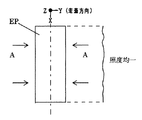
ここで、不活性ガスを走査方向に平行な方向から対向して供給する理由を図2及び図3を用いて説明する。図2及び図3において、重力方向は−Z方向、走査方向は±Y方向であり、EPは露光装置100における露光領域、矢印Aは不活性ガスの供給方向を示している。
【0037】
図2(a)は、露光領域EPの長手方向、即ち、走査方向と直交する方向に対向して不活性ガスを供給した場合を示す概略平面図、図2(b)は、走査方向における露光領域EP内の照度むらを示すグラフである。図2(a)を参照するに、露光領域EPの不活性ガスが供給される近傍と露光領域EPの長手方向の中心部付近とでは、酸素、水分等の濃度分布が異なり、図2(b)に示すような照度むらを生じる。この状態において、走査方向へ露光を行うと照度むらの影響により、露光領域EP内で適正な露光光量が得られないため、正確にパターンを露光することができない。
【0038】
図3(a)は、露光領域EPの走査方向に対向して不活性ガスを供給した場合を示す概略平面図、図3(b)は、走査方向における露光領域EP内の照度むらを示すグラフである。図3(a)を参照するに、露光領域EPの不活性ガスが供給される近傍と露光領域EPの走査方向の中心部付近とでは、酸素、水分等の濃度分布が均一となり、図3(b)に示すように照度が均一となる。この状態において、走査方向へ露光を行うと、露光領域EP内で適正な露光光量が得ることができ、正確にパターンを露光することができる。従って、走査方向に平行な2方向から不活性ガスを供給することによって、酸素、水分等の濃度分布により生じる照度むらの影響を最小限に抑え、スループットの維持、向上を図ることができる。
【0039】
ここで、図3において、ウェハステージを+Y方向に走査している場合、−Y方向から外部空間のガスを巻き込みやすくなる。それを防ぐために、−Y方向に向かって供給する不活性ガスの量を、+Y方向に向かって供給する不活性ガスの量よりも多くすることによって、外部空間からのガスの巻き込みを減らすことができる。この不活性ガスを供給する方向の関係は、ウェハステージを−Y方向に走査している場合は、勿論逆向きになることは明らかであり、ウェハステージの走査方向が切り替わる度に、不活性ガスの供給量を調整するようにすれば良い。また、ウェハステージの走査速度によっても、外部空間からのガスの巻き込み量が変わるので、ウェハステージの走査速度によって不活性ガスを供給する量を変化させても良い。
【0040】
また、空間S2において、不活性ガスを対向して供給することにより、図1に示す矢印Bのような−Z方向への不活性ガスの流れが生じ、包囲部材140とプレート170との間隙CSから不活性ガスが流れ出すため、プレート170のレジストから発生するガス等を光学部材150に寄せ付けず、光学部材150が汚染されることを最小限に抑えることが可能である。これにより、包囲部材140又は光学部材150の交換頻度が少なくなりコストを抑えることができる。
【0041】
なお、光学部材150がプレート170のレジストから発生するガス等により汚染された場合は、包囲部材140又は包囲部材140の保持部141に保持された光学部材150を交換し、光学部材150の汚染による照度劣化及びスループットの低下を防止する。
【0042】
光学部材150がプレート170のレジストから発生するガス等により汚染され、光学部材150又は包囲部材140を交換する際に、光学部材150の曲率が小さく、光学部材150の偏芯精度等が露光装置100の光学性能に多大な影響を及ぼす場合には、光学部材150の調芯作業等が必要となり時間がかかる。そこで、光学部材150を平行平板形状として、調芯作業等を必要しないようようにすることが好ましい。
【0043】
また、包囲部材140のプレート170側の端面において、光軸と直交方向の長さLは、包囲部材140とプレート170との間隙CSの径Cbより大きくなるように設置する。これは、長さLが間隙CSの径Cbより大きければ、間隙CSより空間S2に混入する酸素、水分等の割合が減少し、空間S2のパージ効率がよくなることが実験的にわかったからである。従って、空間S2を効率よくパージすることができ、所望の露光光量を短時間で得ることが可能となる。
【0044】
上述したように、投影光学系130と包囲部材140との接触面に配置した気密部材143も不純物を含んだ周囲のガスが空間S1に混入することを防止し、空間S1のシール性を向上させることで照度劣化を抑制し、スループットを維持、向上させている。
【0045】
投影光学系130の内部の空間、空間S1及びS2に供給される不活性ガスが、露光装置100の光学性能によっては異なる場合がある。かかる場合は、投影光学系130の内部の空間、空間S1及びS2に供給される不活性ガスが混合すると露光光の屈折率が変化し、光学性能の変動を招く。そこで、包囲部材140の保持部141と光学部材150とを接合部材144で接合することで、空間S1と空間S2とを遮断し、不活性ガスが混合することを防止している。
【0046】
再び、図1に戻って、プレート170は、ウェハや液晶基板などの被処理体であり、フォトレジストが塗布されている。フォトレジスト塗布工程は、前処理と、密着性向上剤塗布処理と、フォトレジスト塗布処理と、プリベーク処理とを含む。前処理は、洗浄、乾燥などを含む。密着性向上剤塗布処理は、フォトレジストと下地との密着性を高めるための表面改質(即ち、界面活性剤塗布処理による疎水性化)処理であり、HMDS(Hexamethyl−disilazane)などの有機膜をコート又は蒸気処理する。プリベークは、ベーキング(焼成)工程であるが現像後のそれよりもソフトであり、溶剤を除去する。
【0047】
プレートステージ175は、プレート170を支持する。プレートステージ175は、例えば、リニアモーターを利用してXYZ方向にプレート170を移動させる。レチクル120とプレート170は、例えば、同期走査され、両者は一定の速度比率で駆動される。プレートステージ175は、例えば、ダンパを介して床等の上に支持されるステージ定盤上に設けられる。
【0048】
露光において、光源部112から発せられた光束は、照明光学系114によりレチクル120を、例えば、ケーラー照明する。レチクル120を通過してマスクパターンを反映する光は、投影光学系130により所定の倍率(例えば、1/4又は1/5)で縮小され、プレート170上に結像される。かかる露光がプレート170上の複数の転写領域に対して繰り返し行われる。
【0049】
露光装置100は、露光光の吸収によるプレート170への露光光量の低下及び光学素子G1乃至G6及び光学部材150の汚染を防止することができるので、高い解像力とスループットで経済性よくデバイス(半導体素子、LCD素子、撮像素子(CCDなど)、薄膜磁気ヘッドなど)を提供することができる。
【0050】
次に、図4を参照して、図1に示す露光装置100の変形例である露光装置100Aについて説明する。図4は、図1に示す露光装置100の変形例である露光装置100Aの例示的一形態を示す概略構成図であって、図4(a)は、正面断面図、図4(b)は、下面断面図である。但し、図4において、照明装置110、レチクル120、レチクルステージ125、投影光学系130の内部及びガス供給手段160は図1に示す露光装置100と同じであるため省略している。また、重力方向は−Z方向、走査方向は±Y方向である。
【0051】
図4を参照するに、露光装置100Aは、図1に示す露光装置100と同様であるが、包囲部材140の構成が異なり、プレート170に光軸に対して斜めに検出光KHを照射してプレート170の位置を検出する位置検出手段180を有する。位置検出手段180は、検出光KHを射出する投光部180aと、プレート170で反射された検出光KHを受光する受光部180bから構成される。
【0052】
包囲部材140には、投光部180aから射出される検出光KH及び受光部180bに向かうプレート170で反射された検出光KHを通過させる開口部146が設けられている。しかし、包囲部材140に設けられた開口部146により酸素、水分等が空間S2に混入し、空間S2におけるパージ効率を低下させる場合がある。そこで、検出光KHを透過させると共に投影光学系130(即ち、空間S2)の気密性を維持する光透過部材147を包囲部材140に設置する構成としている。
【0053】
また、開口部146における圧力変化及び温度変化は、位置検出手段180の計測誤差を招き、プレート170の位置調整精度が悪化し、結像性能の劣化の原因となる。そのため、包囲部材140と周囲の不活性ガスの温度差が、位置検出手段180の計測精度に影響を及ぼさない所定の値以下となるように、図示しない温度制御部によって制御する。また、圧力が変動すると、光学性能の変動を招くため、図示しない圧力制御部によって開口部146の圧力が一定となるように制御する。
【0054】
次に、図5及び図6を参照して、図1に示す露光装置100の変形例である露光装置100Bについて説明する。図5は、図1に示す露光装置100の変形例である露光装置100Bの例示的一形態を示す概略構成図である。但し、図5において、照明装置110、レチクル120、レチクルステージ125及び投影光学系130の内部は図1に示す露光装置100と同じであるため省略している。また、重力方向は−Z方向、走査方向は±Y方向である。
【0055】
図5を参照するに、露光装置100Bは、図1に示す露光装置100と同様であるが、包囲部材140の構成が異なる。露光装置100においては、光学部材150の外径全周に亘って包囲部材140の保持部141で保持したが、露光装置100Bでは、光学部材150をセル部材148を介して保持する。
【0056】
セル部材148を介して光学部材150を保持することにより、包囲部材140をボルト142を用いて投影光学系130に締結する際に発生する包囲部材140の応力の光学部材150への伝播を低減させることができる。従って、包囲部材140又は光学部材150の交換前後において、光学部材150の面形状が変化することを最小限に抑え、光学性能の変動を抑制することができる。
【0057】
なお、空間S1と空間S2を遮断するために、セル部材148と光学部材150、セル部材148と包囲部材140とは、接合部材144を用いて接合することが好ましい。接合部材144は、例えば、接着剤等を用いて、酸素、水分等の脱ガスが極小であるものを選定する。
【0058】
図6は、図5に示すセル部材148の例示的一形態を示す概略上面図である。セル部材148は、図6に示すように、光学部材150の光軸を中心として円周方向に沿って等間隔で3箇所に配置された(即ち、120°ピッチで配置された)支持部148aで光学部材150を支持する。従って、光学部材150は、支持部148a上で安定すると共に、光学部材150の自重による面変形形状が予測可能となり、包囲部材140又は光学部材150の交換前後において光学性能の変動を抑えることができる。
【0059】
次に、図7及び図8を参照して、図1に示す露光装置100の変形例である露光装置100Cについて説明する。図7は、図1に示す露光装置100の変形例である露光装置100Cの例示的一形態を示す概略構成図である。但し、図7において、照明装置110、レチクル120、レチクルステージ125は、図1に示す露光装置100と同じであるため省略している。また、重力方向は−Z方向、走査方向は±Y方向である。
【0060】
図7を参照するに、露光装置100Cは、図1に示す露光装置100と同様であるが、ガス供給手段160から空間S2に供給される不活性ガスの供給経路が異なる。露光装置100はガス供給手段160と包囲部材140とを供給配管162を用いて接続し、供給口145を介して空間S2に不活性ガスを供給していたが、図7に示す露光装置100Cはガス供給手段160と鏡筒132に形成した通気孔139とを供給配管162を用いて接続し、かかる通気孔139と包囲部材140に形成した通気孔149を連結することで、通気孔139、通気孔149及び供給口145を介して空間S2に不活性ガスを供給している。これにより、供給配管162の設置によって作業スペースが制約され、包囲部材140又は光学部材150の交換作業の効率が低下することを防止することができる。
【0061】
図8は、図7に示す領域C、即ち、鏡筒132に形成した通気孔139と包囲部材140に形成した通気孔149との連結箇所を示す概略拡大図である。図8を参照するに、通気孔139と通気孔149との連結箇所(即ち、鏡筒132と包囲部材140接触面)には、通気孔139及び通気孔149を跨ぐような2箇所に気密部材143aが設置されている。これは、通気孔139と通気孔149との連結箇所における不活性ガスのもれを防ぎ、空間S2に供給する不活性ガスの圧力変動を最小限に抑えるためである。気密部材143aは、Oリング等が用いられ、材料としては、酸素、水分等の脱ガスが極小であるものを選定することが望ましい。
【0062】
次に、図9及び図10を参照して、上述の露光装置100(露光装置100A乃至100Cも含む)を利用したデバイス製造方法の実施例を説明する。図9は、デバイス(ICやLSIなどの半導体チップ、LCD、CCD等)の製造を説明するためのフローチャートである。ここでは、半導体チップの製造を例に説明する。ステップ1(回路設計)では、デバイスの回路設計を行う。ステップ2(マスク製作)では、設計した回路パターンを形成したマスクを製作する。ステップ3(ウェハ製造)では、シリコンなどの材料を用いてウェハを製造する。ステップ4(ウェハプロセス)は、前工程と呼ばれ、マスクとウェハを用いてリソグラフィー技術によってウェハ上に実際の回路を形成する。ステップ5(組み立て)は、後工程と呼ばれ、ステップ4によって作成されたウェハを半導体チップ化する工程であり、アッセンブリ工程(ダイシング、ボンディング)、パッケージング工程(チップ封入)等の工程を含む。ステップ6(検査)では、ステップ5で作成された半導体デバイスの動作確認テスト、耐久性テストなどの検査を行う。こうした工程を経て半導体デバイスが完成し、それが出荷(ステップ7)される。
【0063】
図10は、ステップ4のウェハプロセスの詳細なフローチャートである。ステップ11(酸化)では、ウェハの表面を酸化させる。ステップ12(CVD)では、ウェハの表面に絶縁膜を形成する。ステップ13(電極形成)では、ウェハ上に電極を蒸着などによって形成する。ステップ14(イオン打ち込み)では、ウェハにイオンを打ち込む。ステップ15(レジスト処理)では、ウェハに感光剤を塗布する。ステップ16(露光)では、露光装置100によってマスクの回路パターンをウェハに露光する。ステップ17(現像)では、露光したウェハを現像する。ステップ18(エッチング)では、現像したレジスト像以外の部分を削り取る。ステップ19(レジスト剥離)では、エッチングが済んで不要となったレジストを取り除く。これらのステップを繰り返し行うことによってウェハ上に多重に回路パターンが形成される。本実施形態のデバイス製造方法によれば、従来よりも高品位のデバイスを製造することができる。
【0064】
以上、本発明の好ましい実施例を説明したが、本発明はこれらに限定されずその要旨の範囲内で様々な変形や変更が可能である。例えば、本発明は、光軸から偏芯した露光領域を有する光学系を有する露光装置にも適用することができる。
【0065】
本出願は、更に以下の事項を開示する。
【0066】
〔実施態様1〕 被処理体を走査しつつ、前記被処理体に露光する走査型の露光装置であって、
前記被処理体の周辺空間を囲う包囲部材と、
前記走査方向に対して実質的に平行な2方向から、前記周辺空間にガスを供給するガス供給手段とを有することを特徴とする露光装置。
【0067】
〔実施態様2〕 前記被処理体と同期してパターンを走査する走査手段と、
前記パターンを前記被処理体に投影する投影光学系とを有しており、
前記包囲部材が、前記投影光学系と前記被処理体との間の空間を囲っていることを特徴とする実施態様1記載の露光装置。
【0068】
〔実施態様3〕 投影光学系に対してパターンが形成されたレチクルと被処理体とを走査することにより、前記パターンを前記被処理体に露光する走査型の露光装置であって、
前記投影光学系と前記被処理体との間に設けられると共に前記被処理体と間隙を形成して配置され、前記投影光学系と協同して前記被処理体の周辺空間の気密性を保持する包囲部材と、
前記周辺空間に、前記走査方向に平行な2方向からガスを供給するガス供給手段とを有することを特徴とする露光装置。
【0069】
〔実施態様4〕 前記包囲部材は、前記投影光学系に着脱可能に接続されることを特徴とする実施態様1乃至3のうちいずれか一項記載の露光装置。
【0070】
〔実施態様5〕 前記投影光学系が有する少なくとも一つの光学部材のうち前記周辺空間に接する光学部材が、平行平板であることを特徴とする実施態様1乃至4のうちいずれか一項記載の露光装置。
【0071】
〔実施態様6〕 前記投影光学系と前記包囲部材との気密性を維持する気密部材を更に有することを特徴とする実施態様2乃至5のうちいずれか一項記載の露光装置。
【0072】
〔実施態様7〕 前記被処理体に対して斜めに光を照射して当該被処理体の位置を検出する位置検出手段と、
前記包囲部材に設けられ、前記位置検出に用いる光を透過させると共に前記周辺空間の気密性を維持する光透過部材とを有することを特徴とする実施態様1乃至6のうちいずれか一項記載の露光装置。
【0073】
〔実施態様8〕 前記ガス供給手段は、前記走査方向に平行で互いに向かい合う2方向から、前記周辺空間にガスを供給することを特徴とする実施態様1乃至7のうちいずれか一項記載の露光装置。
【0074】
〔実施態様9〕 前記被処理体が走査されている方向に供給されるガスの量よりも、前記被処理体が走査されている方向と逆方向に供給されるガスの量の方が多いことを特徴とする実施態様8記載の露光装置。
【0075】
〔実施態様10〕 前記被処理体が走査されている方向に供給されるガスの量及び/又は前記被処理体が走査されている方向と逆方向に供給されるガスの量を、前記被処理体の走査方向及び/又は走査速度によって変化させるガス流量可変手段を有することを特徴とする実施態様8又は9記載の露光装置。
【0076】
〔実施態様11〕 前記ガス供給手段が供給するガスが不活性ガスであることを特徴とする実施態様1乃至10のうちいずれか一項記載の露光装置。
【0077】
〔実施態様12〕 投影光学系に対してパターンが形成されたレチクルと被処理体とを走査することにより、前記パターンを前記被処理体に露光する露光方法であって、
前記投影光学系と前記被処理体との間の周辺空間を気密状態に維持するステップと、
前記周辺空間を前記走査方向に平行な2方向からパージするステップとを有することを特徴とする露光方法。
【0078】
〔実施態様13〕 実施態様1乃至11のうちいずれか一項記載の露光装置を用いて被処理体を露光するステップと、
露光された前記被処理体に所定のプロセスを行うステップとを有することを特徴とするデバイス製造方法。
【0079】
【発明の効果】
本発明によれば、露光光の吸収による被処理体への露光光量の低下及び光学素子の汚染を防止し、スループット及び光学性能に優れた露光装置を提供することができる。
【図面の簡単な説明】
【図1】本発明の一側面としての露光装置の例示的一形態を示す概略構成図であって、図1(a)は、正面断面図、図1(b)は、下面断面図である。
【図2】図2(a)は、露光領域の長手方向、即ち、走査方向と直交する方向に対向して不活性ガスを供給した場合を示す概略平面図、図2(b)は、走査方向における露光領域内の照度むらを示すグラフである。
【図3】図3(a)は、露光領域の走査方向に対向して不活性ガスを供給した場合を示す概略平面図、図3(b)は、走査方向における露光領域内の照度むらを示すグラフである。
【図4】図1に示す露光装置の変形例である露光装置の例示的一形態を示す概略構成図であって、図4(a)は、正面断面図、図4(b)は、下面断面図である。
【図5】図1に示す露光装置の変形例である露光装置の例示的一形態を示す概略構成図である。
【図6】図5に示すセル部材の例示的一形態を示す概略上面図である。
【図7】図1に示す露光装置の変形例である露光装置の例示的一形態を示す概略構成図である。
【図8】図7に示す領域C、即ち、鏡筒に形成した通気孔と包囲部材に形成した通気孔との連結箇所を示す概略拡大図である。
【図9】デバイス(ICやLSIなどの半導体チップ、LCD、CCD等)の製造を説明するためのフローチャートである。
【図10】図9に示すステップ4のウェハプロセスの詳細なフローチャートである。
【図11】従来の露光装置の一部を示す概略構成図である。
【符号の説明】
100、100A乃至C 露光装置
110 照明装置
120 レチクル
125 レチクルステージ
130 投影光学系
132 鏡筒
134 パージ手段
134a 供給ライン
134b 排気ライン
137 接合部材
138 押さえ環
139 通気孔
140 包囲部材
141 保持部
142 ボルト
143及び143a 気密部材
144 接合部材
145 供給口
146 開口部
147 光透過部材
148 セル部材
148a 支持部
149 通気孔
150 光学部材
160 ガス供給手段
162 供給配管
170 プレート
175 プレートステージ
180 位置検出手段
G1乃至G6 光学素子
C1乃至C6 セル部材
J1乃至J5 スペーサ
CS 間隙
S1及びS2 空間[0001]
TECHNICAL FIELD OF THE INVENTION
The present invention generally relates to an exposure apparatus, and more particularly to an exposure apparatus used for exposing an object to be processed such as a single crystal substrate for a semiconductor wafer and a glass substrate for a liquid crystal display (LCD). The present invention is suitable for, for example, an exposure apparatus that uses light having a wavelength of 200 nm or less as an exposure light source.
[0002]
[Prior art]
When manufacturing fine semiconductor elements such as semiconductor memories and logic circuits using photolithography (baking) technology, a circuit pattern drawn on a reticle or a mask (in the present application, these terms are used interchangeably) is used. 2. Description of the Related Art A projection exposure apparatus that transfers a circuit pattern by projecting onto a wafer or the like by a projection optical system has been conventionally used.
[0003]
The resolution (minimum size that can be transferred) of the projection exposure apparatus is proportional to the wavelength of light used for exposure and inversely proportional to the numerical aperture (NA) of the projection optical system. Therefore, the shorter the wavelength, the better the resolution. For this reason, the wavelength of exposure light has been shortened in accordance with the recent demand for miniaturization of semiconductor elements, and the exposure light source is a conventional ultra-high pressure mercury lamp (g-line (wavelength: about 436 nm), i-line (wavelength: about 365 nm). )) To a shorter wavelength KrF excimer laser (wavelength: about 248 nm) or ArF excimer laser (wavelength: about 193 nm). 2 The practical use of lasers (wavelength: about 157 nm) is also progressing.
[0004]
In the case of exposure light having a wavelength of 200 nm or less, the emission spectrum overlaps with the oxygen absorption band, so that oxygen absorbs the exposure light and reduces the amount of exposure light to the object to be processed (decrease in the transmittance of the exposure light). This leads to a decrease in throughput. In addition, the ozone generated by oxygen absorbing the exposure light further increases the absorption of the exposure light, and various products due to the ozone adhere to the surface of the optical element, thereby improving the optical performance of the optical system. It causes deterioration. In particular, F 2 Regarding the laser exposure light, the emission spectrum also overlaps with the absorption band of moisture, moisture absorbs the exposure light like oxygen, and the transmittance of the exposure light and the throughput of the device decrease, and the optical performance of the optical system also decreases. Causes deterioration.
[0005]
Therefore, ArF excimer laser and F 2 In a projection exposure apparatus using a laser or the like as a light source, an inert gas (for example, nitrogen gas, helium gas, argon gas, or the like) is added to the atmosphere of the optical path of the exposure light including the illumination optical system, the projection optical system, and the like. ) To purge (replace) oxygen, moisture and the like present in the optical path. For example, there has been proposed an exposure apparatus in which a space from the photosensitive substrate side end of the projection optical system to the vicinity of the photosensitive substrate is a sealed space, and the sealed space, the projection optical system, and the illumination optical system are purged with an inert gas (for example, an exposure apparatus). And Patent Document 1.).
[0006]
On the other hand, the optical element of the exposure apparatus adheres to the surface by impurities contained in the surrounding atmosphere. It is known that ammonium sulfate, silicon oxide, or the like typically adheres to the surface of the optical element as such a deposit. The optical element is contaminated by these deposits, which causes deterioration of optical performance such as reduction in illuminance and uneven illuminance. One of the sources of impurities is gas generated from the resist on the photosensitive substrate, and in particular, the optical elements of the projection optical system that are closest to the photosensitive substrate are constantly exposed to the gas generated from the resist. The performance is significantly deteriorated.
[0007]
Therefore, there has been proposed an exposure apparatus in which an optical element formed of a parallel flat plate is detachably disposed in an optical path between a projection optical system and a photosensitive substrate, and is replaceable when such an optical element is contaminated ( For example, see Patent Document 2.)
[0008]
Further, there has been proposed an exposure apparatus that absorbs exposure light due to oxygen, moisture, or the like existing in an optical path and prevents contamination of an optical element due to attached matter (for example, see Patent Document 3). Such an exposure apparatus will be described with reference to FIG. FIG. 11 is a schematic configuration diagram showing a part of a conventional exposure apparatus 1000.
[0009]
Referring to FIG. 11, an image of a reticle pattern (not shown) is projected onto a wafer 1200 on a wafer stage 1250 in a wafer chamber 1300 via a projection optical system 1100 under exposure light EL in a vacuum ultraviolet region. You. Between the projection optical system 1100 and the wafer 1200, a blower plate 1400 having an opening 1410 that opens the optical path of the exposure light EL is provided, and gas in the first space H1 above the blower plate 1400 is exhausted. After the gas is exhausted from 1420, an inert gas is supplied from the air supply port 1430 into the first space H1 from a certain direction, so that the gas generated from the wafer 1200 is efficiently exhausted. Further, the inert gas is also supplied into the second space H2 below the blower plate 1400.
[0010]
[Patent Document 1]
JP-A-8-279458
[Patent Document 2]
JP-A-4-36505
[Patent Document 3]
JP 2001-118783 A
[0011]
[Problems to be solved by the invention]
However, the exposure apparatus proposed in Patent Document 1 has a slight air layer between the vicinity of the photosensitive substrate and the photosensitive substrate, and completely purges the space between the projection optical system and the photosensitive substrate with an inert gas. Therefore, the exposure light is absorbed by oxygen, moisture, and the like. In particular, F 2 When a laser is used for the exposure light, the absorption of the exposure light is remarkable even in a minute air layer, and the amount of exposure light to the object to be processed is reduced, resulting in a significant decrease in the throughput of the apparatus.
[0012]
Further, in the exposure apparatus proposed in Patent Document 2, there is no method for preventing contamination of the optical element formed of the plane-parallel plate, and the frequency of replacement of the optical element increases, which causes a problem that the replacement costs a running cost. . In particular, F 2 Glass materials that can be used in wavelength bands such as lasers are limited to calcium fluoride (fluorite), which increases the cost of the glass materials. In addition, the surface resolution of the optical element is also improved by improving the resolution. The processing cost is also high. Therefore, it is not practical unless there is a method for preventing contamination of the optical element formed of the plane-parallel plate.
[0013]
On the other hand, in the exposure apparatus proposed in Patent Document 3, an air supply port 1430 and an exhaust port 1420 are provided in the first space H1 (between the projection optical system 1100 and the blowing plate 1400) to flow gas from a certain direction. However, if the exhaust port 1420 is provided in the first space H1, there is a disadvantage that oxygen, moisture, and the like contained in the surrounding atmosphere are easily taken in, and the purge effect is reduced. Further, a configuration in which the blower plate 1400 and the exhaust port 1420 on the leeward side of the exposure region are eliminated has been proposed, but it is not practical because the surrounding gas is involved and the gas blowing effect at the opening 1410 is significantly reduced. .
[0014]
Accordingly, it is an exemplary object of the present invention to provide an exposure apparatus which is capable of preventing a reduction in the amount of exposure light to be processed and contamination of an optical element due to absorption of exposure light, and having excellent throughput and optical performance.
[0015]
[Means for Solving the Problems]
In order to achieve the above object, an exposure apparatus according to one aspect of the present invention is a scanning type exposure apparatus that exposes an object to be processed while scanning the object to be processed, and a peripheral space of the object to be processed. And gas supply means for supplying gas to the peripheral space from two directions substantially parallel to the scanning direction.
[0016]
Further objects and other features of the present invention will become apparent from preferred embodiments described below with reference to the accompanying drawings.
[0017]
BEST MODE FOR CARRYING OUT THE INVENTION
Hereinafter, an exposure apparatus as one aspect of the present invention will be described with reference to the accompanying drawings. In each of the drawings, the same members are denoted by the same reference numerals, and redundant description will be omitted. Here, FIG. 1 is a schematic configuration diagram showing an exemplary embodiment of an exposure apparatus 100 according to one aspect of the present invention. FIG. 1A is a front sectional view, and FIG. It is sectional drawing. In FIG. 1, the gravity direction is the -Z direction, and the scanning direction is the ± Y direction.
[0018]
As shown in FIG. 1, the exposure apparatus 100 includes an illumination device 110 that illuminates a reticle 120 on which a circuit pattern is formed, a projection optical system 130 that projects diffracted light generated from the illuminated reticle pattern onto a plate 170, It has a member 140, an optical member 150, a gas supply means 160, and a plate stage 170 supporting the plate 170.
[0019]
The exposure apparatus 100 is a scanning projection exposure apparatus (also referred to as a “scanner”) that exposes a circuit pattern formed on the reticle 120 to the plate 170 by a step-and-scan method. Such an exposure apparatus is suitable for a submicron or quarter micron lithography process. Here, the “step-and-scan method” means that a wafer is continuously scanned (scanned) with respect to a reticle to expose a reticle pattern to the wafer, and the wafer is step-moved after one-shot exposure is completed. This is an exposure method for moving to the next exposure area.
[0020]
The illumination device 110 illuminates the reticle 120 on which the transfer circuit pattern is formed, and includes a light source unit 112 and an illumination optical system 114.
[0021]
The light source unit 112 uses, for example, a laser as a light source. The laser is an ArF excimer laser having a wavelength of about 193 nm, a KrF excimer laser having a wavelength of about 248 nm, and an F laser having a wavelength of 153 nm. 2 A laser or the like can be used, but the type of laser is not limited to an excimer laser. For example, a YAG laser may be used, and the number of light sources is not limited. For example, if two solid-state lasers operating independently are used, there is no mutual coherence between the solid-state lasers, and speckle due to coherence is considerably reduced. The optical system may be swung linearly or rotationally to further reduce speckle. When a laser is used for the light source unit 112, a light beam shaping optical system for shaping a parallel light beam from the laser light source into a desired beam shape and an incoherent optical system for making a coherent laser light beam incoherent are used. Is preferred. The light source that can be used for the light source unit 112 is not limited to a laser, and one or more lamps such as a mercury lamp and a xenon lamp can also be used.
[0022]
The illumination optical system 114 is an optical system that illuminates the reticle 120, and includes a lens, a mirror, an optical integrator, a stop, and the like. For example, a condenser lens, a fly-eye lens, an aperture stop, a condenser lens, a slit, and an imaging optical system are arranged in this order. The illumination optical system 114 can be used regardless of on-axis light or off-axis light. The optical integrator uniformly illuminates the reticle 120 with a predetermined numerical aperture, and includes an integrator configured by stacking a fly-eye lens and two sets of cylindrical lens array (or lenticular lens) plates. It may be replaced by a diffraction element.
[0023]
The reticle 120 is made of, for example, quartz, has a circuit pattern (or image) to be transferred formed thereon, and is supported and driven by the reticle stage 125. Diffracted light emitted from the reticle 120 passes through the projection optical system 130 and is projected onto the plate 170. The reticle 120 and the plate 170 are in an optically conjugate relationship. Since the exposure apparatus 100 is a scanner, the pattern of the reticle 120 is transferred onto the plate 170 by scanning the reticle 120 and the plate 170 at a reduction ratio.
[0024]
The reticle stage 125 supports the reticle 120 and is connected to a moving mechanism (not shown). As the reticle stage 125, any configuration known in the art can be applied. The moving mechanism (not shown) is configured by a linear motor or the like, and can move the reticle 120 by driving the reticle stage 125 in at least the ± Y direction. Exposure apparatus 100 scans reticle 120 and plate 170 in a synchronized state.
[0025]
The projection optical system 130 reduces and projects the circuit pattern formed on the reticle 120 onto the plate 170. The projection optical system 130 includes an optical system including only a plurality of lens elements, an optical system including a plurality of lens elements and at least one concave mirror (catadioptric optical system), a plurality of lens elements and at least one kinoform. For example, an optical system having a diffractive optical element such as an optical system, an all-mirror optical system, or the like can be used. When chromatic aberration needs to be corrected, a plurality of lens elements made of glass materials having different dispersion values (Abbe values) from each other may be used, or the diffractive optical element may be configured to cause dispersion in a direction opposite to that of the lens element. I do.
[0026]
In this embodiment, the projection optical system 130 includes optical elements G1 to G6, cell members C1 to C6, a lens barrel 132, and a purge unit 134.
[0027]
The optical elements G1 to G6 are mounted on cell members C1 to C6 to be described later, and form an image of light using refraction, reflection, diffraction, and the like. The optical elements G1 to G6 are joined and fixed and held by the joining member 137 over the circumference of the cell members C1 to C6. However, regarding the method of fixing the optical elements G1 to G6, a leaf spring or a retaining ring (not shown) may be used.
[0028]
The cell members C1 to C6 are annular members centered on the optical axis, and are spacers J1 for adjusting the distance between the optical elements G1 and G2, and adjust the distance between the optical elements G2 and G3. J2 for adjusting the distance between the optical element G3 and the optical element G4, the spacer J4 for adjusting the distance between the optical element G4 and the optical element G5, and the spacer J2 for adjusting the distance between the optical element G4 and the optical element G6. It is held by a spacer J5 for adjusting the interval and the lens barrel 132, and is fixed to the lens barrel 132 by a retaining ring 138.
[0029]
The lens barrel 132 houses the optical elements G1 to G6 via the cell members C1 to C6. The lens barrel 132 has an airtight structure by the optical element G1 closest to the object plane and the optical element G2 closest to the image plane, and forms a space of an atmosphere different from the outside. The cell members C1 to C6 are formed with through holes (not shown), and the spaces of the optical elements G1 to G6 are communicated with the through holes.
[0030]
The purging unit 134 has a supply line 134a for supplying an inert gas to the projection optical system 130 and an exhaust line 134b for exhausting the inert gas supplied to the projection optical system 130. Is replaced with an inert gas. As the inert gas, for example, helium, nitrogen, argon and the like are used. In particular, when helium gas is used, the density is lower than that of the atmosphere. Therefore, as shown in FIG. 1, replacement is facilitated by using a flow path that flows from the upper part to the lower part of the space inside the lens barrel 132.
[0031]
The enclosing member 140 is provided between the projection optical system 130 and the plate 170 and is arranged so as to form a gap CS with the plate 170, and encloses the optical path space between the projection optical system 130 and the plate 170. The surrounding member 140 has a holding portion 141 on which an optical member 150 described later is placed, and keeps the airtightness of the projection optical system 130 in cooperation with the optical member 150.
[0032]
The surrounding member 140 is provided with a supply port 145 for introducing a gas supplied by a gas supply unit 160 described later into a space between the projection optical system 130 and the plate 170 formed by the surrounding member 140. The supply ports 145 are arranged so as to face each other in parallel with the scanning direction.
[0033]
The surrounding member 140 is fastened to the projection optical system 130 by bolts 142 and is detachable. When the surrounding member 140 is fastened to the projection optical system 130, the airtight member 143 is installed. This is for improving the sealing performance on the contact surface between the projection optical system 130 and the surrounding member 140 and maintaining the airtightness between the projection optical system 130 and the surrounding member 140. As the hermetic member 143, an O-ring or the like is used, and as the material, it is desirable to select a material that has minimal degassing such as oxygen and moisture.
[0034]
The optical member 150 is mounted on the holding unit 142 and transmits exposure light emitted from the projection optical system 130. The optical member 150 is joined to the holding portion 141 of the surrounding member 140 using the joining member 144 over the entire outer diameter. Thereby, the space between the projection optical system 130 and the plate 170 formed by the surrounding member 140 is separated into a space S1 between the projection optical system 130 and the optical member 150 and a space S2 between the optical member 150 and the plate 170. Is done. This is to prevent deterioration of illuminance caused by contamination of the optical elements G1 to G6 due to gas or the like generated from the resist of the plate 170 being mixed into the projection optical system 130.
[0035]
The gas supply unit 160 supplies gas to a space formed by the surrounding member 140 and the optical member 150 from two directions parallel to the scanning direction. In the present embodiment, the gas supply unit 160 is connected to the supply port 145 via the supply pipe 162, and supplies an inert gas whose pressure, flow rate, and temperature are controlled to the space S2. Therefore, in the space S2, the inert gas is supplied from the supply port 145 of the surrounding member 140 in a direction parallel to the scanning direction, and the inert gas supplied from the gap CS is exhausted. Oxygen, moisture, etc. remaining in the air are efficiently discharged.
[0036]
Here, the reason why the inert gas is supplied to be opposed from a direction parallel to the scanning direction will be described with reference to FIGS. 2 and 3, the gravitational direction is the -Z direction, the scanning direction is the ± Y direction, EP indicates an exposure area in the exposure apparatus 100, and an arrow A indicates a supply direction of the inert gas.
[0037]
FIG. 2A is a schematic plan view showing a case where an inert gas is supplied in the longitudinal direction of the exposure region EP, that is, in a direction orthogonal to the scanning direction. FIG. 6 is a graph showing illuminance unevenness in an area EP. Referring to FIG. 2A, the concentration distribution of oxygen, moisture, and the like is different between the vicinity of the exposure region EP to which the inert gas is supplied and the vicinity of the longitudinal center of the exposure region EP. ) Causes uneven illuminance. In this state, if exposure is performed in the scanning direction, an appropriate amount of exposure light cannot be obtained within the exposure area EP due to uneven illuminance, so that the pattern cannot be accurately exposed.
[0038]
FIG. 3A is a schematic plan view showing a case where an inert gas is supplied in the scanning direction of the exposure area EP, and FIG. 3B is a graph showing illuminance unevenness in the exposure area EP in the scanning direction. It is. Referring to FIG. 3A, the concentration distribution of oxygen, moisture, and the like becomes uniform between the vicinity of the exposure region EP to which the inert gas is supplied and the vicinity of the center of the exposure region EP in the scanning direction. Illuminance becomes uniform as shown in b). In this state, when exposure is performed in the scanning direction, an appropriate amount of exposure light can be obtained in the exposure area EP, and the pattern can be accurately exposed. Accordingly, by supplying the inert gas from two directions parallel to the scanning direction, it is possible to minimize the influence of illuminance unevenness caused by the concentration distribution of oxygen, moisture, and the like, and to maintain and improve the throughput.
[0039]
Here, in FIG. 3, when the wafer stage is scanned in the + Y direction, gas in the external space is easily entrained from the −Y direction. In order to prevent this, the amount of the inert gas supplied in the −Y direction is made larger than the amount of the inert gas supplied in the + Y direction to reduce the entrainment of the gas from the external space. it can. Obviously, the relationship between the directions in which the inert gas is supplied is reversed when the wafer stage is scanned in the −Y direction. Each time the scanning direction of the wafer stage is switched, the inert gas is switched. May be adjusted. In addition, the amount of gas entrained from the external space changes depending on the scanning speed of the wafer stage. Therefore, the amount of the inert gas to be supplied may be changed according to the scanning speed of the wafer stage.
[0040]
In addition, by supplying the inert gas in the space S2 in a facing manner, the flow of the inert gas in the −Z direction as shown by the arrow B in FIG. 1 is generated, and the gap CS between the surrounding member 140 and the plate 170 is generated. Since an inert gas flows out of the optical member 150, gas generated from the resist on the plate 170 does not approach the optical member 150, so that contamination of the optical member 150 can be minimized. Thus, the frequency of replacing the surrounding member 140 or the optical member 150 is reduced, and the cost can be reduced.
[0041]
When the optical member 150 is contaminated by gas or the like generated from the resist on the plate 170, the optical member 150 held by the surrounding member 140 or the holding portion 141 of the surrounding member 140 is replaced, and the optical member 150 is contaminated. This prevents illuminance degradation and throughput reduction.
[0042]
When the optical member 150 is contaminated by gas or the like generated from the resist on the plate 170 and the optical member 150 or the surrounding member 140 is replaced, the curvature of the optical member 150 is small, and the eccentricity and the like of the optical member 150 are reduced. When the optical performance of the optical member 150 is greatly affected, alignment work of the optical member 150 and the like are required, and it takes time. Therefore, it is preferable that the optical member 150 is formed in a parallel plate shape so that an alignment operation or the like is not required.
[0043]
In addition, on the end surface of the surrounding member 140 on the plate 170 side, the length L in the direction orthogonal to the optical axis is set to be larger than the diameter Cb of the gap CS between the surrounding member 140 and the plate 170. This is because, when the length L is larger than the diameter Cb of the gap CS, it has been experimentally found that the ratio of oxygen, moisture and the like mixed into the space S2 is reduced from the gap CS, and the purge efficiency of the space S2 is improved. . Therefore, the space S2 can be efficiently purged, and a desired exposure light amount can be obtained in a short time.
[0044]
As described above, the airtight member 143 disposed on the contact surface between the projection optical system 130 and the surrounding member 140 also prevents the surrounding gas containing impurities from entering the space S1 and improves the sealing property of the space S1. As a result, illuminance degradation is suppressed, and throughput is maintained and improved.
[0045]
The inert gas supplied to the space inside the projection optical system 130 and the spaces S1 and S2 may differ depending on the optical performance of the exposure apparatus 100. In such a case, if the inert gas supplied to the space inside the projection optical system 130 and the spaces S1 and S2 is mixed, the refractive index of the exposure light changes, causing a change in optical performance. Therefore, by joining the holding member 141 of the surrounding member 140 and the optical member 150 with the joining member 144, the space S1 and the space S2 are shut off, thereby preventing the inert gas from being mixed.
[0046]
Returning to FIG. 1 again, the plate 170 is an object to be processed such as a wafer or a liquid crystal substrate, and is coated with a photoresist. The photoresist application step includes a pretreatment, an adhesion improver application process, a photoresist application process, and a pre-bake process. The pretreatment includes washing, drying, and the like. The adhesion improver application treatment is a surface modification (that is, a hydrophobic treatment by a surfactant application treatment) for improving the adhesion between the photoresist and the base, and is an organic film such as HMDS (Hexamethyl-disilazane). Is coated or steamed. Prebaking is a baking (firing) step, but is softer than that after development, and removes the solvent.
[0047]
The plate stage 175 supports the plate 170. The plate stage 175 moves the plate 170 in the XYZ directions using, for example, a linear motor. The reticle 120 and the plate 170 are, for example, synchronously scanned, and both are driven at a constant speed ratio. The plate stage 175 is provided on a stage base supported on a floor or the like via a damper, for example.
[0048]
In the exposure, the light beam emitted from the light source unit 112 illuminates the reticle 120 with, for example, Koehler illumination by the illumination optical system 114. Light that passes through the reticle 120 and reflects the mask pattern is reduced at a predetermined magnification (for example, 倍率 or 5) by the projection optical system 130 and is imaged on the plate 170. Such exposure is repeatedly performed on a plurality of transfer areas on the plate 170.
[0049]
The exposure apparatus 100 can prevent a decrease in the amount of exposure light to the plate 170 due to absorption of exposure light and prevent contamination of the optical elements G1 to G6 and the optical member 150. , An LCD element, an imaging element (such as a CCD), a thin-film magnetic head, etc.).
[0050]
Next, an exposure apparatus 100A which is a modification of the exposure apparatus 100 shown in FIG. 1 will be described with reference to FIG. FIG. 4 is a schematic configuration diagram showing an exemplary form of an exposure apparatus 100A which is a modification of the exposure apparatus 100 shown in FIG. 1, wherein FIG. 4 (a) is a front sectional view, and FIG. FIG. However, in FIG. 4, the illumination device 110, the reticle 120, the reticle stage 125, the inside of the projection optical system 130, and the gas supply means 160 are the same as those in the exposure apparatus 100 shown in FIG. The gravity direction is the -Z direction, and the scanning direction is the ± Y direction.
[0051]
Referring to FIG. 4, an exposure apparatus 100A is similar to the exposure apparatus 100 shown in FIG. 1, but has a different configuration of a surrounding member 140, and irradiates a plate 170 with detection light KH obliquely with respect to an optical axis. It has a position detecting means 180 for detecting the position of the plate 170. The position detecting means 180 includes a light projecting unit 180a that emits the detection light KH and a light receiving unit 180b that receives the detection light KH reflected by the plate 170.
[0052]
The surrounding member 140 is provided with an opening 146 through which the detection light KH emitted from the light projecting unit 180a and the detection light KH reflected by the plate 170 toward the light receiving unit 180b pass. However, there are cases where oxygen, moisture, and the like are mixed into the space S2 by the opening 146 provided in the surrounding member 140, and the purge efficiency in the space S2 is reduced. Therefore, the light transmitting member 147 that transmits the detection light KH and maintains the airtightness of the projection optical system 130 (that is, the space S2) is provided in the surrounding member 140.
[0053]
Further, a change in pressure and a change in temperature at the opening 146 cause a measurement error of the position detection unit 180, deteriorates the position adjustment accuracy of the plate 170, and causes deterioration of the imaging performance. Therefore, the temperature control unit (not shown) controls the temperature difference between the surrounding member 140 and the surrounding inert gas to be equal to or less than a predetermined value that does not affect the measurement accuracy of the position detection unit 180. In addition, if the pressure fluctuates, the optical performance fluctuates. Therefore, a pressure control unit (not shown) controls the pressure in the opening 146 to be constant.
[0054]
Next, an exposure apparatus 100B which is a modification of the exposure apparatus 100 shown in FIG. 1 will be described with reference to FIGS. FIG. 5 is a schematic configuration diagram showing an exemplary form of an exposure apparatus 100B which is a modification of the exposure apparatus 100 shown in FIG. However, in FIG. 5, the interiors of the illumination device 110, the reticle 120, the reticle stage 125, and the projection optical system 130 are omitted because they are the same as those of the exposure apparatus 100 shown in FIG. The gravity direction is the -Z direction, and the scanning direction is the ± Y direction.
[0055]
Referring to FIG. 5, exposure apparatus 100B is similar to exposure apparatus 100 shown in FIG. 1, but the configuration of surrounding member 140 is different. In the exposure apparatus 100, the optical member 150 is held by the holding portion 141 of the surrounding member 140 over the entire outer diameter of the optical member 150. In the exposure apparatus 100B, the optical member 150 is held via the cell member 148.
[0056]
By holding the optical member 150 via the cell member 148, the propagation of the stress of the surrounding member 140 generated when the surrounding member 140 is fastened to the projection optical system 130 using the bolt 142 to the optical member 150 is reduced. be able to. Therefore, a change in the surface shape of the optical member 150 before and after the replacement of the surrounding member 140 or the optical member 150 can be minimized, and a change in optical performance can be suppressed.
[0057]
In order to block the space S1 and the space S2, it is preferable that the cell member 148 and the optical member 150 and the cell member 148 and the surrounding member 140 are joined using the joining member 144. As the joining member 144, for example, an adhesive or the like is used, and a member having minimal degassing such as oxygen and moisture is selected.
[0058]
FIG. 6 is a schematic top view showing an exemplary embodiment of the cell member 148 shown in FIG. As shown in FIG. 6, the cell members 148 are provided at three locations (ie, at 120 ° pitch) at equal intervals along the circumferential direction around the optical axis of the optical member 150 (ie, at 120 ° pitches). Supports the optical member 150. Therefore, the optical member 150 is stabilized on the support portion 148a, and the surface deformation shape due to the own weight of the optical member 150 can be predicted, and the fluctuation of the optical performance before and after the replacement of the surrounding member 140 or the optical member 150 can be suppressed. .
[0059]
Next, an exposure apparatus 100C which is a modification of the exposure apparatus 100 shown in FIG. 1 will be described with reference to FIGS. FIG. 7 is a schematic configuration diagram showing an exemplary form of an exposure apparatus 100C which is a modification of the exposure apparatus 100 shown in FIG. However, in FIG. 7, the illumination device 110, the reticle 120, and the reticle stage 125 are omitted because they are the same as the exposure device 100 shown in FIG. The gravity direction is the -Z direction, and the scanning direction is the ± Y direction.
[0060]
Referring to FIG. 7, exposure apparatus 100C is the same as exposure apparatus 100 shown in FIG. 1, but the supply path of the inert gas supplied from gas supply means 160 to space S2 is different. Exposure apparatus 100 connects gas supply means 160 and surrounding member 140 using supply pipe 162, and supplies inert gas to space S2 through supply port 145. However, exposure apparatus 100C shown in FIG. The gas supply means 160 is connected to the ventilation hole 139 formed in the lens barrel 132 using a supply pipe 162, and the ventilation hole 139 is connected to the ventilation hole 149 formed in the surrounding member 140, so that the ventilation hole 139 is formed. The inert gas is supplied to the space S2 through the pores 149 and the supply port 145. Accordingly, the work space is restricted by the installation of the supply pipe 162, and it is possible to prevent the efficiency of the replacement work of the surrounding member 140 or the optical member 150 from being reduced.
[0061]
FIG. 8 is a schematic enlarged view showing a region C shown in FIG. 7, that is, a connecting portion between a vent 139 formed in the lens barrel 132 and a vent 149 formed in the surrounding member 140. Referring to FIG. 8, the airtight member is provided at two places where the air hole 139 and the air hole 149 are connected to each other (that is, the contact surface between the lens barrel 132 and the surrounding member 140). 143a is provided. This is to prevent the leakage of the inert gas at the connection point between the vent 139 and the vent 149 and to minimize the fluctuation of the pressure of the inert gas supplied to the space S2. An O-ring or the like is used for the hermetic member 143a, and it is desirable to select a material that minimizes outgassing such as oxygen and moisture.
[0062]
Next, an embodiment of a device manufacturing method using the above-described exposure apparatus 100 (including the exposure apparatuses 100A to 100C) will be described with reference to FIGS. FIG. 9 is a flowchart for explaining the manufacture of devices (semiconductor chips such as ICs and LSIs, LCDs, CCDs, etc.). Here, the manufacture of a semiconductor chip will be described as an example. In step 1 (circuit design), the circuit of the device is designed. Step 2 (mask fabrication) forms a mask on which the designed circuit pattern is formed. In step 3 (wafer manufacturing), a wafer is manufactured using a material such as silicon. Step 4 (wafer process) is referred to as a preprocess, and an actual circuit is formed on the wafer by lithography using the mask and the wafer. Step 5 (assembly) is called a post-process, and is a process of converting the wafer created in step 4 into semiconductor chips, and includes processes such as an assembly process (dicing and bonding) and a packaging process (chip encapsulation). In step 6 (inspection), inspections such as an operation check test and a durability test of the semiconductor device created in step 5 are performed. Through these steps, a semiconductor device is completed and shipped (step 7).
[0063]
FIG. 10 is a detailed flowchart of the wafer process in Step 4. Step 11 (oxidation) oxidizes the wafer's surface. Step 12 (CVD) forms an insulating film on the surface of the wafer. Step 13 (electrode formation) forms electrodes on the wafer by vapor deposition or the like. Step 14 (ion implantation) implants ions into the wafer. In step 15 (resist processing), a photosensitive agent is applied to the wafer. Step 16 (exposure) uses the exposure apparatus 100 to expose a circuit pattern on the mask onto the wafer. Step 17 (development) develops the exposed wafer. Step 18 (etching) removes portions other than the developed resist image. Step 19 (resist stripping) removes unnecessary resist after etching. By repeating these steps, multiple circuit patterns are formed on the wafer. According to the device manufacturing method of the present embodiment, it is possible to manufacture a higher-quality device than before.
[0064]
Although the preferred embodiments of the present invention have been described above, the present invention is not limited thereto, and various modifications and changes can be made within the scope of the gist. For example, the present invention can be applied to an exposure apparatus having an optical system having an exposure area decentered from the optical axis.
[0065]
The present application further discloses the following matters.
[0066]
[Embodiment 1] A scanning type exposure apparatus that exposes an object to be processed while scanning the object to be processed,
An enclosing member surrounding a peripheral space of the object to be processed;
An exposure apparatus, comprising: gas supply means for supplying gas to the peripheral space from two directions substantially parallel to the scanning direction.
[0067]
[Embodiment 2] Scanning means for scanning a pattern in synchronization with the object to be processed,
A projection optical system for projecting the pattern onto the object to be processed,
The exposure apparatus according to claim 1, wherein the surrounding member surrounds a space between the projection optical system and the object.
[0068]
[Embodiment 3] A scanning exposure apparatus that exposes the pattern to the object by scanning the reticle having the pattern formed on the projection optical system and the object,
It is provided between the projection optical system and the object to be processed and is arranged so as to form a gap with the object to be processed, and cooperates with the projection optical system to maintain airtightness of a peripheral space of the object to be processed. An enclosing member;
An exposure apparatus, comprising: gas supply means for supplying gas to the peripheral space from two directions parallel to the scanning direction.
[0069]
[Embodiment 4] The exposure apparatus according to any one of Embodiments 1 to 3, wherein the surrounding member is detachably connected to the projection optical system.
[0070]
[Embodiment 5] The exposure according to any one of Embodiments 1 to 4, wherein an optical member in contact with the peripheral space among at least one optical member of the projection optical system is a parallel flat plate. apparatus.
[0071]
[Embodiment 6] The exposure apparatus according to any one of Embodiments 2 to 5, further comprising an airtight member for maintaining the airtightness between the projection optical system and the surrounding member.
[0072]
[Embodiment 7] Position detection means for irradiating the object to be processed with light obliquely and detecting the position of the object to be processed,
7. The light-transmitting member according to claim 1, further comprising: a light-transmitting member provided on the surrounding member to transmit light used for the position detection and maintain airtightness of the peripheral space. Exposure equipment.
[0073]
[Eighth Embodiment] The exposure according to any one of the first to seventh embodiments, wherein the gas supply unit supplies gas to the peripheral space from two directions parallel to the scanning direction and facing each other. apparatus.
[0074]
[Embodiment 9] The amount of gas supplied in the direction opposite to the direction in which the object is scanned is larger than the amount of gas supplied in the direction in which the object is scanned. The exposure apparatus according to embodiment 8, wherein:
[0075]
[Embodiment 10] The amount of gas supplied in the direction in which the object is scanned and / or the amount of gas supplied in the direction opposite to the direction in which the object is scanned is determined by the amount of the gas to be processed. The exposure apparatus according to the eighth or ninth embodiment, further comprising a gas flow rate varying unit that varies according to a scanning direction and / or a scanning speed of the body.
[0076]
[Embodiment 11] The exposure apparatus according to any one of Embodiments 1 to 10, wherein the gas supplied by the gas supply unit is an inert gas.
[0077]
[Embodiment 12] An exposure method for exposing the object to be processed by scanning the object and the reticle on which the pattern is formed with respect to a projection optical system,
Maintaining a peripheral space between the projection optical system and the processing object in an airtight state,
Purging the peripheral space from two directions parallel to the scanning direction.
[0078]
[Embodiment 13] A step of exposing a workpiece using the exposure apparatus according to any one of Embodiments 1 to 11,
Performing a predetermined process on the exposed object to be processed.
[0079]
【The invention's effect】
According to the present invention, it is possible to provide an exposure apparatus which is capable of preventing a reduction in the amount of exposure light to a workpiece and a contamination of an optical element due to absorption of exposure light, and having excellent throughput and optical performance.
[Brief description of the drawings]
FIG. 1 is a schematic configuration diagram showing an exemplary embodiment of an exposure apparatus as one aspect of the present invention, wherein FIG. 1 (a) is a front sectional view, and FIG. 1 (b) is a bottom sectional view. .
FIG. 2A is a schematic plan view showing a case where an inert gas is supplied in a direction opposite to a longitudinal direction of an exposure region, that is, a direction orthogonal to a scanning direction, and FIG. 6 is a graph showing illuminance unevenness in an exposure area in a direction.
FIG. 3A is a schematic plan view showing a case where an inert gas is supplied so as to face an exposure region in a scanning direction, and FIG. 3B shows illuminance unevenness in the exposure region in the scanning direction. It is a graph shown.
4A and 4B are schematic configuration diagrams illustrating an exemplary embodiment of an exposure apparatus that is a modified example of the exposure apparatus illustrated in FIG. 1; FIG. 4A is a front cross-sectional view, and FIG. It is sectional drawing.
FIG. 5 is a schematic configuration diagram showing an exemplary embodiment of an exposure apparatus which is a modification of the exposure apparatus shown in FIG.
FIG. 6 is a schematic top view showing an exemplary embodiment of the cell member shown in FIG.
FIG. 7 is a schematic configuration diagram illustrating an exemplary embodiment of an exposure apparatus that is a modification of the exposure apparatus illustrated in FIG.
8 is a schematic enlarged view showing a region C shown in FIG. 7, that is, a connecting portion between a vent formed in the lens barrel and a vent formed in the surrounding member.
FIG. 9 is a flowchart for explaining the manufacture of devices (semiconductor chips such as ICs and LSIs, LCDs, CCDs, and the like).
FIG. 10 is a detailed flowchart of a wafer process in Step 4 shown in FIG. 9;
FIG. 11 is a schematic configuration diagram showing a part of a conventional exposure apparatus.
[Explanation of symbols]
100, 100A-C Exposure apparatus
110 Lighting device
120 reticle
125 reticle stage
130 Projection optical system
132 lens barrel
134 purging means
134a supply line
134b exhaust line
137 Joining member
138 retaining ring
139 Vent
140 Surrounding member
141 Holder
142 volts
143 and 143a Airtight members
144 joining members
145 Supply port
146 opening
147 Light transmission member
148 cell member
148a support
149 vent
150 Optical member
160 gas supply means
162 supply piping
170 plates
175 plate stage
180 position detecting means
G1 to G6 optical element
C1 to C6 cell member
J1 to J5 spacer
CS gap
S1 and S2 space