JP2004253780A - Semiconductor device and its manufacturing method - Google Patents
Semiconductor device and its manufacturing method Download PDFInfo
- Publication number
- JP2004253780A JP2004253780A JP2003420838A JP2003420838A JP2004253780A JP 2004253780 A JP2004253780 A JP 2004253780A JP 2003420838 A JP2003420838 A JP 2003420838A JP 2003420838 A JP2003420838 A JP 2003420838A JP 2004253780 A JP2004253780 A JP 2004253780A
- Authority
- JP
- Japan
- Prior art keywords
- film
- atm
- semiconductor device
- silicon carbonitride
- interlayer insulating
- Prior art date
- Legal status (The legal status is an assumption and is not a legal conclusion. Google has not performed a legal analysis and makes no representation as to the accuracy of the status listed.)
- Pending
Links
- 239000004065 semiconductor Substances 0.000 title claims abstract description 74
- 238000004519 manufacturing process Methods 0.000 title claims description 29
- 229910052710 silicon Inorganic materials 0.000 claims abstract description 98
- 239000010703 silicon Substances 0.000 claims abstract description 93
- XUIMIQQOPSSXEZ-UHFFFAOYSA-N Silicon Chemical compound [Si] XUIMIQQOPSSXEZ-UHFFFAOYSA-N 0.000 claims abstract description 88
- IJGRMHOSHXDMSA-UHFFFAOYSA-N Atomic nitrogen Chemical compound N#N IJGRMHOSHXDMSA-UHFFFAOYSA-N 0.000 claims abstract description 76
- 239000011229 interlayer Substances 0.000 claims abstract description 63
- 229910052757 nitrogen Inorganic materials 0.000 claims abstract description 39
- 230000004888 barrier function Effects 0.000 claims description 76
- 229910052751 metal Inorganic materials 0.000 claims description 63
- 239000002184 metal Substances 0.000 claims description 63
- 239000010410 layer Substances 0.000 claims description 40
- 238000000034 method Methods 0.000 claims description 39
- -1 polysiloxane Polymers 0.000 claims description 24
- 229920001296 polysiloxane Polymers 0.000 claims description 22
- 239000000470 constituent Substances 0.000 claims description 19
- 229910052718 tin Inorganic materials 0.000 claims description 19
- 229910052739 hydrogen Inorganic materials 0.000 claims description 17
- 229910052782 aluminium Inorganic materials 0.000 claims description 16
- 239000000758 substrate Substances 0.000 claims description 12
- 238000012545 processing Methods 0.000 claims description 7
- 229910000881 Cu alloy Inorganic materials 0.000 claims description 6
- 230000007423 decrease Effects 0.000 claims description 6
- 150000004767 nitrides Chemical class 0.000 claims description 5
- 229910052790 beryllium Inorganic materials 0.000 claims description 4
- 229910052793 cadmium Inorganic materials 0.000 claims description 4
- 229910052799 carbon Inorganic materials 0.000 claims description 4
- 229910052737 gold Inorganic materials 0.000 claims description 4
- 229910052753 mercury Inorganic materials 0.000 claims description 4
- 229910052763 palladium Inorganic materials 0.000 claims description 4
- 229910052697 platinum Inorganic materials 0.000 claims description 4
- 229910052719 titanium Inorganic materials 0.000 claims description 4
- 229910052725 zinc Inorganic materials 0.000 claims description 4
- 229910052726 zirconium Inorganic materials 0.000 claims description 4
- BLRPTPMANUNPDV-UHFFFAOYSA-N Silane Chemical compound [SiH4] BLRPTPMANUNPDV-UHFFFAOYSA-N 0.000 claims description 3
- 229910000077 silane Inorganic materials 0.000 claims description 3
- 238000010521 absorption reaction Methods 0.000 abstract description 22
- 230000000694 effects Effects 0.000 abstract description 14
- 150000003376 silicon Chemical class 0.000 abstract description 5
- 230000008878 coupling Effects 0.000 abstract 2
- 238000010168 coupling process Methods 0.000 abstract 2
- 238000005859 coupling reaction Methods 0.000 abstract 2
- 230000006866 deterioration Effects 0.000 abstract 1
- 239000010408 film Substances 0.000 description 472
- 239000010949 copper Substances 0.000 description 105
- 229910004298 SiO 2 Inorganic materials 0.000 description 57
- 229920002120 photoresistant polymer Polymers 0.000 description 20
- 238000010586 diagram Methods 0.000 description 19
- 238000005268 plasma chemical vapour deposition Methods 0.000 description 16
- ATJFFYVFTNAWJD-UHFFFAOYSA-N Tin Chemical compound [Sn] ATJFFYVFTNAWJD-UHFFFAOYSA-N 0.000 description 15
- 238000005530 etching Methods 0.000 description 15
- UFHFLCQGNIYNRP-UHFFFAOYSA-N Hydrogen Chemical compound [H][H] UFHFLCQGNIYNRP-UHFFFAOYSA-N 0.000 description 13
- 230000000903 blocking effect Effects 0.000 description 13
- 239000001257 hydrogen Substances 0.000 description 13
- 238000000206 photolithography Methods 0.000 description 12
- 239000005360 phosphosilicate glass Substances 0.000 description 11
- 229910052814 silicon oxide Inorganic materials 0.000 description 11
- 239000007789 gas Substances 0.000 description 10
- 229910010271 silicon carbide Inorganic materials 0.000 description 9
- 238000004544 sputter deposition Methods 0.000 description 9
- 238000007747 plating Methods 0.000 description 8
- 238000001157 Fourier transform infrared spectrum Methods 0.000 description 7
- 238000004380 ashing Methods 0.000 description 7
- HBMJWWWQQXIZIP-UHFFFAOYSA-N silicon carbide Chemical compound [Si+]#[C-] HBMJWWWQQXIZIP-UHFFFAOYSA-N 0.000 description 7
- 238000000137 annealing Methods 0.000 description 6
- QVGXLLKOCUKJST-UHFFFAOYSA-N atomic oxygen Chemical compound [O] QVGXLLKOCUKJST-UHFFFAOYSA-N 0.000 description 6
- 238000007872 degassing Methods 0.000 description 6
- 150000002500 ions Chemical class 0.000 description 6
- 239000001301 oxygen Substances 0.000 description 6
- 229910052760 oxygen Inorganic materials 0.000 description 6
- RYGMFSIKBFXOCR-UHFFFAOYSA-N Copper Chemical group [Cu] RYGMFSIKBFXOCR-UHFFFAOYSA-N 0.000 description 5
- XAGFODPZIPBFFR-UHFFFAOYSA-N aluminium Chemical compound [Al] XAGFODPZIPBFFR-UHFFFAOYSA-N 0.000 description 5
- 150000001412 amines Chemical class 0.000 description 5
- 229910052802 copper Inorganic materials 0.000 description 5
- 238000010304 firing Methods 0.000 description 5
- 230000003647 oxidation Effects 0.000 description 5
- 238000007254 oxidation reaction Methods 0.000 description 5
- 239000002356 single layer Substances 0.000 description 5
- 238000012360 testing method Methods 0.000 description 5
- 238000005406 washing Methods 0.000 description 5
- 239000013039 cover film Substances 0.000 description 4
- NBVXSUQYWXRMNV-UHFFFAOYSA-N fluoromethane Chemical compound FC NBVXSUQYWXRMNV-UHFFFAOYSA-N 0.000 description 4
- 239000000203 mixture Substances 0.000 description 4
- 229910018182 Al—Cu Inorganic materials 0.000 description 3
- HMDDXIMCDZRSNE-UHFFFAOYSA-N [C].[Si] Chemical compound [C].[Si] HMDDXIMCDZRSNE-UHFFFAOYSA-N 0.000 description 3
- 230000009977 dual effect Effects 0.000 description 3
- 238000005001 rutherford backscattering spectroscopy Methods 0.000 description 3
- 238000005033 Fourier transform infrared spectroscopy Methods 0.000 description 2
- VYPSYNLAJGMNEJ-UHFFFAOYSA-N Silicium dioxide Chemical compound O=[Si]=O VYPSYNLAJGMNEJ-UHFFFAOYSA-N 0.000 description 2
- 238000004833 X-ray photoelectron spectroscopy Methods 0.000 description 2
- 230000007547 defect Effects 0.000 description 2
- 238000009792 diffusion process Methods 0.000 description 2
- KPUWHANPEXNPJT-UHFFFAOYSA-N disiloxane Chemical class [SiH3]O[SiH3] KPUWHANPEXNPJT-UHFFFAOYSA-N 0.000 description 2
- 238000009826 distribution Methods 0.000 description 2
- 239000000428 dust Substances 0.000 description 2
- 238000010030 laminating Methods 0.000 description 2
- 239000000463 material Substances 0.000 description 2
- 239000002245 particle Substances 0.000 description 2
- 230000002265 prevention Effects 0.000 description 2
- 238000001228 spectrum Methods 0.000 description 2
- 238000003860 storage Methods 0.000 description 2
- OKTJSMMVPCPJKN-UHFFFAOYSA-N Carbon Chemical compound [C] OKTJSMMVPCPJKN-UHFFFAOYSA-N 0.000 description 1
- 244000132059 Carica parviflora Species 0.000 description 1
- 235000014653 Carica parviflora Nutrition 0.000 description 1
- PXGOKWXKJXAPGV-UHFFFAOYSA-N Fluorine Chemical compound FF PXGOKWXKJXAPGV-UHFFFAOYSA-N 0.000 description 1
- 229910018557 Si O Inorganic materials 0.000 description 1
- 229910052581 Si3N4 Inorganic materials 0.000 description 1
- DHXVGJBLRPWPCS-UHFFFAOYSA-N Tetrahydropyran Chemical compound C1CCOCC1 DHXVGJBLRPWPCS-UHFFFAOYSA-N 0.000 description 1
- 229910045601 alloy Inorganic materials 0.000 description 1
- 239000000956 alloy Substances 0.000 description 1
- 239000005441 aurora Substances 0.000 description 1
- 238000005229 chemical vapour deposition Methods 0.000 description 1
- 238000000576 coating method Methods 0.000 description 1
- 238000007796 conventional method Methods 0.000 description 1
- 230000003247 decreasing effect Effects 0.000 description 1
- 238000013461 design Methods 0.000 description 1
- 230000002542 deteriorative effect Effects 0.000 description 1
- 239000010432 diamond Substances 0.000 description 1
- 238000002474 experimental method Methods 0.000 description 1
- 229910052731 fluorine Inorganic materials 0.000 description 1
- 239000011737 fluorine Substances 0.000 description 1
- 239000011521 glass Substances 0.000 description 1
- 239000011261 inert gas Substances 0.000 description 1
- 229910010272 inorganic material Inorganic materials 0.000 description 1
- 239000011147 inorganic material Substances 0.000 description 1
- 238000007689 inspection Methods 0.000 description 1
- 238000003475 lamination Methods 0.000 description 1
- 239000007788 liquid Substances 0.000 description 1
- 230000007774 longterm Effects 0.000 description 1
- 230000003287 optical effect Effects 0.000 description 1
- 239000011368 organic material Substances 0.000 description 1
- 238000013021 overheating Methods 0.000 description 1
- 229910052698 phosphorus Inorganic materials 0.000 description 1
- 239000002994 raw material Substances 0.000 description 1
- 229920006395 saturated elastomer Polymers 0.000 description 1
- SCPYDCQAZCOKTP-UHFFFAOYSA-N silanol Chemical compound [SiH3]O SCPYDCQAZCOKTP-UHFFFAOYSA-N 0.000 description 1
- LIVNPJMFVYWSIS-UHFFFAOYSA-N silicon monoxide Inorganic materials [Si-]#[O+] LIVNPJMFVYWSIS-UHFFFAOYSA-N 0.000 description 1
- HQVNEWCFYHHQES-UHFFFAOYSA-N silicon nitride Chemical compound N12[Si]34N5[Si]62N3[Si]51N64 HQVNEWCFYHHQES-UHFFFAOYSA-N 0.000 description 1
- 238000004611 spectroscopical analysis Methods 0.000 description 1
- 230000006641 stabilisation Effects 0.000 description 1
- 238000011105 stabilization Methods 0.000 description 1
- PQDJYEQOELDLCP-UHFFFAOYSA-N trimethylsilane Chemical compound C[SiH](C)C PQDJYEQOELDLCP-UHFFFAOYSA-N 0.000 description 1
Images


Landscapes
- Internal Circuitry In Semiconductor Integrated Circuit Devices (AREA)
Abstract
Description
本発明は、半導体装置および半導体装置の製造方法に関し、特に低誘電率層間絶縁膜および低誘電率バリア絶縁膜を用いた配線構造の信頼性の高い半導体装置および、その製造方法に関する。 The present invention relates to a semiconductor device and a method for manufacturing a semiconductor device, and more particularly to a semiconductor device having a highly reliable wiring structure using a low dielectric constant interlayer insulating film and a low dielectric constant barrier insulating film, and a method for manufacturing the same.
近年、LSIの信号処理の高速化の要求は年々増加している。LSIの信号処理速度は主にトランジスタ自体の動作速度および配線での信号伝播遅延時間の大小で決まってくる。従来、大きく影響を及ぼしてきたトランジスタの動作速度はトランジスタを縮小化することで向上させてきた。しかし設計ルールが0.25ミクロンよりも小さいLSIでは後者の配線の信号伝播遅延に関する影響が大きく現れ始めている。特に配線層が多層化を有するLSIデバイスにおいては、その影響は大きい。 In recent years, demands for high-speed LSI signal processing have been increasing year by year. The signal processing speed of the LSI is mainly determined by the operation speed of the transistor itself and the magnitude of the signal propagation delay time in the wiring. Conventionally, the operating speed of a transistor, which has had a great influence, has been improved by reducing the size of the transistor. However, in an LSI having a design rule smaller than 0.25 μm, the influence of the latter wiring on the signal propagation delay has begun to appear significantly. In particular, the effect is great in an LSI device having a multilayer wiring layer.
そこで、配線の信号伝播遅延を改善する方法として、従来より用いてきたアルミ配線が銅配線に置き換わった。また従来から用いていたシリコン酸化膜を低誘電率層間絶縁膜に置き換える検討がされている。この低誘電率膜の中で比誘電率3.0以下が実現できる膜の1つの水素化ポリシロキサンはアルミ配線では量産化が実施されており、Cu配線でも量産化が検討されている。その中でも梯子型水素化ポリシロキサンであるL−Ox(ラダーオキサイド、商標名:Ladder Oxide)はSi−O骨格にSi−H結合を一部にもつもので、無機材料で構成されているため、有機材料より配線金属との密着性に優れ、また梯子型になっているため加工後のプラズマアッシングや有機剥離液に対する耐性がすぐれ、加工面での吸湿層などの劣化層が形成されない。 Therefore, as a method of improving the signal propagation delay of the wiring, the aluminum wiring which has been conventionally used has been replaced with a copper wiring. In addition, studies are being made to replace a conventionally used silicon oxide film with a low dielectric constant interlayer insulating film. Among the low dielectric constant films, one of the films capable of realizing a relative dielectric constant of 3.0 or less has been mass-produced for aluminum wiring, and mass production of Cu wiring has been studied. Among them, L-Ox (ladder oxide, trade name: Ladder Oxide), which is a ladder-type hydrogenated polysiloxane, has a Si-H bond in a part of a Si-O skeleton and is made of an inorganic material. It has better adhesion to wiring metal than organic materials, and since it is a ladder type, it has excellent resistance to plasma ashing and organic stripping liquid after processing, and does not form a deteriorated layer such as a moisture absorbing layer on the processed surface.
一方、Cuダマシンプロセス用のCuの拡散防止兼エッチングのストッパー膜として機能するバリア絶縁膜にも低誘電率化が要求されており、従来の比誘電率が約7.0のシリコン窒化膜から比誘電率5.0以下のシリコン炭化膜(以下、SiC膜と記載)系絶縁膜への置き換えの検討が行われている。一例として、トリメチルシランと不活性ガスによるプラズマCVDで成膜する例が報告されている。特に微細化のCu/Low−k(低誘電率層間絶縁膜)構造の信頼性まで保証するとなると、上記低誘電率層間絶縁膜およびバリア絶縁膜の組み合わせの最適化ができて初めて量産化が実現できる。 On the other hand, a barrier insulating film which functions as a stopper film for Cu diffusion prevention and etching for the Cu damascene process is also required to have a low dielectric constant, which is lower than that of a conventional silicon nitride film having a relative dielectric constant of about 7.0. Consideration has been given to replacement with a silicon carbide film (hereinafter, referred to as a SiC film) based dielectric film having a dielectric constant of 5.0 or less. As an example, an example in which a film is formed by plasma CVD using trimethylsilane and an inert gas has been reported. In particular, if the reliability of the miniaturized Cu / Low-k (low dielectric constant interlayer insulating film) structure can be guaranteed, mass production is realized only after the combination of the low dielectric constant interlayer insulating film and the barrier insulating film can be optimized. it can.
次に、従来の低誘電率層間絶縁膜およびバリア絶縁膜を使用した半導体装置の構造一例を図面を参照して説明する。図14に示すように、下層絶縁膜501上にCuの拡散防止兼エッチングのストッパー膜として機能する第0のバリア絶縁膜502が形成されており、その上に第1の低誘電率膜503が形成されている。さらにその上に第1のSiO2膜504が形成されている。上記第0のバリア絶縁膜502、第1の低誘電率膜503、第1のSiO2膜504が積層されてなる層間絶縁膜には配線用溝が形成されており、この配線用溝には第1のバリアメタル膜505が形成されている。その内側に第1のCu膜506により第1のCu配線が埋め込み形成されている。このCu配線の上に第1のバリア絶縁膜507、その上に同様に第2の低誘電率膜508、第2のSiO2膜509がそれぞれ形成されている。
Next, an example of the structure of a conventional semiconductor device using a low dielectric constant interlayer insulating film and a barrier insulating film will be described with reference to the drawings. As shown in FIG. 14, a zero barrier
上記第1のバリア絶縁膜507、第2の低誘電率膜508、第2のSiO2膜509が積層されてなる層間絶縁膜にはビア用溝が形成されており、このビア用溝には上記Cu配線同様に第2のバリアメタル膜510、その内側に第2のCu膜511が埋め込み形成されている。さらにこのビアの上に第2のバリア絶縁膜512、その上に同様に第3の低誘電率膜513、第3のSiO2膜514がそれぞれ形成されている。同様に上記第2のバリア絶縁膜512、第3の低誘電率膜513、第3のSiO2膜514が積層されてなる配線層間絶縁膜中に第3のバリアメタル膜515、その内側に第3のCu膜516が埋め込まれ第2のCu配線が形成されている。この第2のCu配線上に、第3のバリア絶縁膜517が形成されている。この構造をさらに必要に応じて繰り返し、最上層配線(本形態では第2のCu溝配線に相当)上および最上層L−Ox膜(本形態では第3の低誘電率膜に相当)上にバリア絶縁膜が形成される。そして、最上層配線上にはバリア絶縁膜に設けた開口を介してSiO2膜518中に形成されたアルミボンディングパッド520(上下にTiN層519,521を有する)が接続され、このアルミボンディングパッド520の一部を除きSiO2膜522を介して吸湿ブロック性のあるカバー膜523(SiON膜またはSiN膜)で被覆され多層配線構造が形成される。
A via groove is formed in the interlayer insulating film formed by laminating the first
次に、上記従来の半導体装置の製造方法を図15から図18を参照して説明する。まず、トランジスタを含む半導体基板上に形成された下層絶縁膜601上に、50nm〜100nmの膜厚の第0のバリア絶縁膜602をプラズマCVD法により形成した。続いて、第1の低誘電率膜603の塗布・焼成を行ない、150nm〜350nmの成膜を行った。その上に、第1SiO2膜604を50nm〜200nmプラズマCVD法により成膜した(図15(a))。
Next, a method for manufacturing the above-described conventional semiconductor device will be described with reference to FIGS. First, a 0-th
この構造体上に、最小寸法0.14μmレベルのフォトリソグラフィー技術を用い、反射防止膜としてARC膜605を塗布後に、パターニングされたフォトレジストマスク606を形成した(図15(b))。これをマスクにして、ARC膜605、第1のSiO2膜604、第1の低誘電率膜603をフロロカーボン系ガスを含んだガスによりエッチングし、第0のバリア絶縁膜602上でストップさせた。
An
その後、酸素プラズマアッシングにより、フォトレジストマスクを剥離後、弱アミンの有機剥離液などで残さ等を完全に除去した。その後、全面エッチバックにて、第0のバリア絶縁膜602を除去した。さらに有機剥離液による洗浄で残さを除去した。この結果、第1配線用の溝パターンを形成した(図15(c))。
Then, after removing the photoresist mask by oxygen plasma ashing, the residue and the like were completely removed with an organic stripping solution of a weak amine or the like. After that, the 0th
次に、スパッタ装置にてデガス処理、ArイオンによるRFエッチを行なった後に第1のバリアメタル膜607を約30nm形成し、真空を破ることなく、Cuシード膜(図示省略)を約100nm形成した。次にCuめっきにて、Cuめっき膜609を約600nm形成した。その後、縦型炉アニールにて200〜400℃で焼成を行った(図16(a))。
Next, after performing degassing and RF etching with Ar ions using a sputtering apparatus, a first
次にメタルCMP技術を用い、溝以外のメタルを除去し第1のCu溝配線609を形成した(図16(b))。次に、プラズマCVD装置により、50〜100nmの第1のバリア絶縁膜610を形成した。続いて、第2の低誘電率膜611、さらに第2のSiO2膜612を順次成膜した。第1のビア形成のためにフォトリソグラフィー技術を用い、ビアのパターンとして第2のARC膜613上に第2のフォトレジストマスク614を形成した(図16(c))。
Next, using a metal CMP technique, the metal other than the groove was removed to form a first Cu groove wiring 609 (FIG. 16B). Next, a first to 100 nm thick
これをマスクにして、第2のARC膜613、 第2のSiO2膜612、第2の低誘電率膜611をエッチングし、第1のバリア絶縁膜610上でエッチストップさせ、第1のビア用溝を開口した。その後、酸素プラズマアッシングにより、フォトレジストマスクを剥離後、アミン系の有機剥離液などで残さ等を完全に除去した。
Using this as a mask, the second ARC
その後、第1のビア用溝底部の第1のバリア絶縁膜610を除去し、第1のCu溝配線との電気的な導通を取るため全面エッチバックをおこなった。さらに有機剥離液による洗浄で残さを除去し、第1のビア用の溝パターンを形成した。続いて、スパッタ装置にてデガスを行なった後、ArイオンによるRFエッチを行なった後に第2のバリアメタル膜615を約30nm形成し、真空を破ることなく、Cuシード膜(図示省略)を約100nm形成した。次にCuめっきにて、銅膜617を約300nm形成した。その後、縦型炉アニールにて200〜400℃で焼成をおこなった。次にメタルCMP技術を用い、ビア部以外のメタルを除去しビア617を形成した(図17(a))。
After that, the first
次に、プラズマCVD装置により、50〜100nmの第2のバリア絶縁膜618を形成した。続いて、第3の低誘電率膜619、さらに第3のSiO2膜620を順次成膜した(図17(b))。
Next, a second
この構造体上に、最小L/S=0.14/0.14μmレベルのフォトリソグラフィー技術を用い、第3のARC膜621塗布後に、パターニングされた第3のフォトレジストマスク622を形成した(図18(a))。
After applying the
これをマスクにして、第3のARC膜621、第3のSiO2膜620、第3の低誘電率膜619をフロロカーボン系ガスを含むエッチングガスによりでエッチングし、第2のバリア絶縁膜618上でストップさせ、第2配線用の溝パターンを開口した。その後、酸素プラズマアッシングにより、フォトレジストマスクを剥離後、アミン系の有機剥離液などで残さ等を完全に除去した。
Using this as a mask, the
その後、全面エッチバックにて、第2配線用溝底部の第2のバリア絶縁膜618を除去した。さらに有機剥離液による洗浄で残さを除去した。この結果、第2溝配線パターンを形成した。次に、第1配線と同様にしてスパッタ装置にてデガス処理、ArイオンによるRFエッチを行なった後に第3のバリアメタル膜623を約30nm形成し、真空を破ることなく、Cuシード膜を約100nm形成した。次にCuめっきにて、Cu膜624を約600nm形成した。その後、縦型炉アニールにて200〜400℃で焼成を行った。その後メタルCMPを行い第2Cu溝配線を形成し、この第2Cu溝配線の上に第3のバリア絶縁膜625が形成されている(図18(b))。
After that, the second
その後第3のバリア絶縁膜625上に300〜500nmのSiO2層間絶縁膜をプラズマCVD法により形成し、第3のバリア絶縁膜625およびSiO2層間絶縁膜にフォトリソグラフィー技術を用い第2Cu溝配線上に開口を設けるためのフォトレジストマスクを形成した。続いて露出したSiO2層間絶縁膜および第3のバリア絶縁膜625をエッチングして第2Cu溝配線とボンディングパッドとを接続するための開口部を形成した。フォトレジストマスク除去後スパッタリング法によりTiN膜519を100〜200nm,Al−Cu(0.5%)膜520を800〜1000nm、TiN膜521を50〜100nmを順次成膜した。続いて、フォトリソグラフィー技術を用いボンディングパッドを形成するためのフォトレジストマスクを形成し、エッチング工程によりボンディングパッドを形成後フォトレジストマスクを除去した。そして、ボンディングパッド上のTiN膜521を覆うようにSiO2膜522を100〜200nm、SiON膜523を100〜200nmプラズマCVD法により順次形成し、フォトリソグラフィー技術によりボンディングパッド上のSiON膜、SiO2膜およびTiN膜521の所定領域を開口しボンディングパッドを露出させ、図14の半導体装置を得た。
Thereafter, an SiO 2 interlayer insulating film having a thickness of 300 to 500 nm is formed on the third
上記従来の半導体装置の製造方法は、シングルダマシン法の一例であるが、デュアルダマシン法による製造方法も公知である。特許文献1には、低誘電率の層間絶縁膜としてフッ素をドーピングしたシリコンガラス(FSG)、低誘電率のバリア膜としてSiC膜を用いたデュアルダマシン構造の半導体装置が記載されている。また、特許文献2には、低誘電率の層間絶縁膜として炭素をドーピングした酸化シリコン、エッチングストッパーを兼ねるバリア膜としてシリコン、炭素、窒素および水素を含有するアモルファス材料を用いた半導体装置が記載されている。
上記2層配線構造の半導体装置を製造するにあたり、本発明者が低誘電率の層間絶縁膜としてL−Ox膜を、バリア絶縁膜としてSiC膜を使用したところ、製造プロセスに長時間を要することにより、電気特性上問題が発生した。また、絶縁膜の種類にかかわらず、Cu配線の表面および界面が酸化された。特に、ビア抵抗の上昇と配線間容量の増大が発生するという問題があった。 In manufacturing the semiconductor device having the above-described two-layer wiring structure, the present inventor used an L-Ox film as an interlayer insulating film having a low dielectric constant and an SiC film as a barrier insulating film. As a result, a problem occurred in the electrical characteristics. Further, regardless of the type of the insulating film, the surface and the interface of the Cu wiring were oxidized. In particular, there is a problem that the via resistance increases and the capacitance between wirings increases.
本発明は、長時間の製造プロセスを要しても配線間容量の上昇やCu配線の酸化等が抑制された半導体装置およびその製造方法を提供することを目的としている。 SUMMARY OF THE INVENTION An object of the present invention is to provide a semiconductor device in which an increase in capacitance between wirings and oxidation of Cu wirings and the like are suppressed even when a long manufacturing process is required, and a method for manufacturing the same.
本発明の半導体装置は、半導体基板を含んだ下地上に、Si−H結合を有する層間絶縁膜を有し、上記層間絶縁膜上にシリコン炭化窒化膜が形成されていることを特徴とする。また、半導体基板を含んだ下地上に、Si−H結合を有する層間絶縁膜を有し、上記層間絶縁膜に形成された溝内にCuを主たる構成元素とする導電膜が埋設され、上記導電膜上にシリコン炭化窒化膜が形成されていることを特徴とする。上記層間絶縁膜および導電膜は各々複数層形成されており、上記シリコン炭化窒化膜は最上層の上記導電膜および層間絶縁膜を各々被覆するように形成されていることを特徴とする。このシリコン炭化窒化膜の窒素濃度は、10atm%以上35atm%未満であり、より好ましくは15atm%以上30atm%未満、また、その他の組成がSiが22atm%以上27atm%以下、Cが20atm%以上25atm%以下、Hが35atm%以上45atm%以下の範囲であることが好ましい。また、シリコン炭化窒化膜は、さらにOを0.5atm%以上5atm%未満含有することを特徴とする。Si−H結合を有する層間絶縁膜は、水素化シロキサンが梯子型水素化シロキサンまたはポーラス梯子型水素化シロキサンであることを特徴とする。上記Si−H結合を有する層間絶縁膜とCuを主たる構成元素とする導電膜との間に金属窒素化膜を有し、上記Cuを主たる構成元素とする導電膜と上記金属窒化膜との間に金属膜を有することが好ましい。Cuを主たる構成元素とする導電膜は、Al、Si、Ag、W、Mg、Bi、Zn、Pd、Cd、Au、Hg、Be、Pt、Zr、Ti、またはSnの少なくとも一つを含むCuアロイ膜であることを特徴とする。また、上記Cuを主たる構成元素とする導電膜が、Siを含むCuアロイ膜であり、Si濃度が導電膜の上面で最も高く、底面方向に深くなるにつれて低くなっていることを特徴とする。 The semiconductor device of the present invention is characterized in that an interlayer insulating film having a Si-H bond is provided on a base including a semiconductor substrate, and a silicon carbonitride film is formed on the interlayer insulating film. In addition, an interlayer insulating film having a Si—H bond is provided over a base including a semiconductor substrate, and a conductive film containing Cu as a main constituent element is buried in a groove formed in the interlayer insulating film. A silicon carbonitride film is formed on the film. A plurality of interlayer insulating films and conductive films are formed, and the silicon carbonitride film is formed so as to cover the uppermost conductive film and interlayer insulating film, respectively. The nitrogen concentration of this silicon carbonitride film is 10 atm% or more and less than 35 atm%, and more preferably 15 atm% or more and less than 30 atm%. %, And H is preferably in the range of 35 atm% to 45 atm%. Further, the silicon carbonitride film is characterized by further containing O at 0.5 atm% or more and less than 5 atm%. The interlayer insulating film having a Si—H bond is characterized in that the siloxane hydride is a ladder-type hydrogenated siloxane or a porous ladder-type hydrogenated siloxane. A metal nitride film is provided between the interlayer insulating film having the Si-H bond and the conductive film containing Cu as a main constituent element, and between the conductive film containing Cu as a main constituent element and the metal nitride film. Preferably has a metal film. The conductive film containing Cu as a main constituent element includes Cu containing at least one of Al, Si, Ag, W, Mg, Bi, Zn, Pd, Cd, Au, Hg, Be, Pt, Zr, Ti, and Sn. It is an alloy film. Further, the conductive film containing Cu as a main constituent element is a Cu alloy film containing Si, wherein the Si concentration is the highest on the upper surface of the conductive film and decreases as the depth increases in the bottom direction.
本発明の半導体装置の製造方法は、半導体基板上にSi−H結合を有する層間絶縁膜を成膜する工程と、上記層間絶縁膜上にシリコン炭化窒化膜を成膜する工程と、を含むことを特徴とする。また、半導体基板上にSi−H結合を有する層間絶縁膜を成膜する第1の工程と、上記層間絶縁膜を加工する第2の工程と、バリアメタル膜を成膜する第3の工程と、Cuを主たる構成元素とする導電膜を成膜する第4の工程と、上記導電膜上にシリコン炭化窒化膜を成膜する第5の工程と、を含むことを特徴とする。上記第2の工程は、上記層間絶縁膜に溝を加工する工程であり、上記第3の工程は、上記溝の側壁および底面にバリアメタル膜を成膜する工程であり、上記第4の工程は、上記バリアメタル膜が成膜された溝内に上記導電膜を埋設する工程であり、上記第5の工程は、上記層間絶縁膜および導電膜上にシリコン炭化窒化膜を成膜する工程であることを特徴とする。上記Cuを主たる構成元素とする導電膜は、Cu膜にシラン処理を施されたSi含有膜であることを特徴とする。 The method of manufacturing a semiconductor device according to the present invention includes a step of forming an interlayer insulating film having a Si—H bond on a semiconductor substrate, and a step of forming a silicon carbonitride film on the interlayer insulating film. It is characterized by. A first step of forming an interlayer insulating film having a Si—H bond on the semiconductor substrate; a second step of processing the interlayer insulating film; and a third step of forming a barrier metal film. , A fourth step of forming a conductive film containing Cu as a main constituent element, and a fifth step of forming a silicon carbonitride film on the conductive film. The second step is a step of processing a groove in the interlayer insulating film, the third step is a step of forming a barrier metal film on a side wall and a bottom surface of the groove, and the fourth step Is a step of burying the conductive film in a groove in which the barrier metal film is formed, and the fifth step is a step of forming a silicon carbonitride film on the interlayer insulating film and the conductive film. There is a feature. The conductive film containing Cu as a main constituent element is a Si-containing film obtained by subjecting a Cu film to a silane treatment.
本発明者は、従来の半導体装置を長時間製造プロセスにより製造した際に発生した配線間容量の上昇やCu配線の酸化の原因を追求した結果、従来の半導体装置を構成するL−Ox膜、SiO2膜、SiC膜のいずれも吸湿に対してブロック性をもたないためであることをつきとめた。即ち、吸湿により、配線間容量の上昇やCu配線の酸化がもたらされたものであることをつきとめた。本発明では、L−Ox膜に代表される水素化ポリシロキサンのようなSi−H結合を有する層間絶縁膜の上層にシリコン炭化窒化膜を用いている。このシリコン炭化窒化膜は、吸湿のブロック性が有るため、下層に水素化ポリシロキサンのような耐吸湿性のない膜が存在しても、外部から湿気が耐吸湿性のない膜に浸透することを抑制し、そのため配線間容量の増大を抑制することができる。また、このシリコン炭化窒化膜は、Cuを主たる構成元素とする導電膜上に形成されている。導電膜表面が耐吸湿性を有する膜に覆われているため、導電膜の酸化が抑制される。さらに、ビア抵抗上昇などの問題も発生しない。層間絶縁膜中のSi−H結合が多いほど、上記効果は顕著に認められる。したがって、Si−H結合を有する層間絶縁膜を低誘電率膜として使用する場合、バリア絶縁膜としてシリコン炭化窒化膜を組合せて使用することが、湿度の影響による電気的特性の低下のない高い信頼性を有する半導体装置を提供するのに好適である。シリコン炭化窒化膜は、最上層の導電膜およびSi−H結合を有する層間絶縁膜を被覆するように形成することが好ましい。 The present inventor pursued a cause of an increase in inter-wiring capacitance and an oxidation of Cu wiring generated when a conventional semiconductor device was manufactured by a long-term manufacturing process, and as a result, an L-Ox film constituting the conventional semiconductor device was obtained. It has been found that neither the SiO 2 film nor the SiC film has a blocking property against moisture absorption. That is, it was found that the moisture absorption caused an increase in the capacitance between wirings and oxidation of the Cu wirings. In the present invention, a silicon carbonitride film is used as an upper layer of an interlayer insulating film having an Si-H bond such as hydrogenated polysiloxane represented by an L-Ox film. Since this silicon carbonitride film has a moisture-absorbing property, even if a film having no moisture resistance such as hydrogenated polysiloxane exists in the lower layer, moisture can penetrate from outside into the moisture-absorbing film. , And an increase in inter-wiring capacitance can be suppressed. This silicon carbonitride film is formed on a conductive film containing Cu as a main constituent element. Since the surface of the conductive film is covered with the moisture-resistant film, oxidation of the conductive film is suppressed. Further, there is no problem such as an increase in via resistance. The above effect is remarkably recognized as the number of Si—H bonds in the interlayer insulating film increases. Therefore, when an interlayer insulating film having a Si—H bond is used as a low dielectric constant film, it is highly reliable to use a combination of a silicon carbonitride film as a barrier insulating film without deteriorating electrical characteristics due to humidity. It is suitable for providing a semiconductor device having a property. The silicon carbonitride film is preferably formed so as to cover the uppermost conductive film and the interlayer insulating film having a Si—H bond.
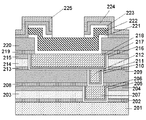
次に、本発明の半導体装置の実施の形態について図面を参照して説明する。図1は、本発明の半導体装置の第1の実施形態を示す図である。図1に示すように、下層絶縁膜101上にエッチングストッパーを兼ねるバリア絶縁膜として第0のシリコン炭化窒化膜(Si,C,N,Hを主たる構成元素として含有する絶縁膜)102が形成されており、その上に梯子型水素化ポリシロキサンである第1のL−Ox膜103が形成されている。その上に第1のSiO2膜104が形成されている。この第0のシリコン炭化窒化膜102、第1のL−Ox膜103、第1のSiO2膜104に形成された第1の配線用溝には第1のバリアメタル膜としてTa膜106/TaN膜105の積層膜(上層がTa膜、下層がTaN膜)が形成されている。その内側に第1のCu膜107が埋め込まれCu配線が形成されている。この第1のCu溝配線の上にバリア絶縁膜である第1のシリコン炭化窒化膜108、その上に同様に第2のL−Ox膜109、第2のSiO2膜110がそれぞれ積層形成され、これらにビア用溝が開口されている。
Next, embodiments of the semiconductor device of the present invention will be described with reference to the drawings. FIG. 1 is a diagram showing a first embodiment of a semiconductor device of the present invention. As shown in FIG. 1, a zeroth silicon carbonitride film (an insulating film containing Si, C, N, and H as a main constituent element) 102 is formed on a lower insulating
同様にビア部に第2のバリアメタル膜としてTa 膜112/TaN膜111、その内側に第2のCu膜113が埋め込まれビアが形成されている。さらに、そのビアの上にバリア絶縁膜である第2のシリコン炭化窒化膜114、その上に同様に第3のL−Ox膜115、第3のSiO2膜116がそれぞれ積層形成されている。同様に第2のシリコン炭化窒化膜114、第3のL−Ox膜115、第3のSiO2膜116に形成された第2の配線用溝には第3のバリアメタル膜としてTa膜118/TaN膜117、その内側に第3のCu膜119が埋め込まれ第2のCu溝配線が形成されている。この第2のCu溝配線上に、第3のシリコン炭化窒化膜120が形成されている。この構造をさらに必要に応じて繰り返し、最上層配線(本実施形態では第2のCu溝配線に相当)上および最上層L−Ox膜(本実施形態では第3のL−Ox膜に相当)上にシリコン炭化窒化膜が形成される。そして、最上層配線上にはシリコン炭化窒化膜に設けた開口を介してアルミボンディングパッド123が接続され、このアルミボンディングパッド123(一例としてアルミの上下にバリアメタル膜としてTiN層122,124を有する構造を図示しているが、この構成に限定されるものではない)の一部を除きSiO2膜125を介して吸湿ブロック性のあるカバー膜126(SiON膜またはSiN膜)で被覆され多層配線構造が形成される。得られた半導体装置は、従来の半導体装置で認められた配線間容量の増大やビア抵抗の上昇は認められなかった。
Similarly, a via is formed by burying a
第2の実施の形態による半導体装置の構造を図2に示す。第1の実施の形態との違いはビア層間絶縁膜をSiO2単層にしたことである。製造のTATが非常に長い場合に電気特性の安定、信頼性の安定にこの構造はメリットがあった。その理由は、ビア工程での吸湿が電気特性や信頼性に影響を与えているためと推定される。 FIG. 2 shows the structure of the semiconductor device according to the second embodiment. The difference from the first embodiment is that the via interlayer insulating film is a single layer of SiO 2 . This structure has an advantage in stabilization of electrical characteristics and stability of reliability when the manufactured TAT is very long. It is presumed that the reason is that moisture absorption in the via process affects electrical characteristics and reliability.
この半導体装置は下層絶縁膜201上に第0のシリコン炭化窒化膜202が形成されており、その上に梯子型水素化ポリシロキサンである第1のL−Ox膜203が形成されている。その上に第1のSiO2膜204が形成されている。第0のシリコン炭化窒化膜202、第1のL−Ox膜203、第1のSiO2膜204に形成された配線溝には第1のバリアメタル膜としてTa膜206/TaN膜205の積層膜(上層がTa膜、下層がTaN膜)が形成されている。その内側にCu膜が埋め込まれた第1のCu溝配線207が形成されている。この第1のCu溝配線の上にバリア絶縁膜である第1のシリコン炭化窒化膜208、その上に第2のSiO2膜209が形成されている。第1のシリコン炭化窒化膜208および第2のSiO2膜209にはビア用溝が形成されており、同様にビア部に第2のバリアメタル膜としてTa膜211/TaN膜210、その内側に第2のCu膜212が埋め込まれビアが形成されている。
In this semiconductor device, a zeroth
さらにそのビアの上にバリア絶縁膜である第2のシリコン炭化窒化膜213、その上に同様に第3のL−Ox膜214、第3のSiO2膜215がそれぞれ積層形成されている。同様に第2のシリコン炭化窒化膜213、第3のL−Ox膜214、第3のSiO2膜215に第3のバリアメタル膜としてTa膜217/TaN膜216、その内側に第3のCu膜218が埋め込まれ第2のCu溝配線が形成されている。この第2のCu溝配線上に、第3のシリコン炭化窒化膜219が形成されている。この構造をさらに必要に応じて繰り返し、最上層配線(本実施形態では第2のCu溝配線に相当)上および最上層L−Ox膜(本実施形態では第3のL−Ox膜に相当)上にシリコン炭化窒化膜が形成される。そして、最上層配線上にはシリコン炭化窒化膜に設けた開口を介してアルミボンディングパッド222が接続され、このアルミボンディングパッド222(一例としてアルミの上下にバリアメタル膜としてTiN層221,223を有する構造を図示しているが、この構成に限定されるものではない)の一部を除きSiO2膜224を介して吸湿ブロック性のあるカバー膜225(SiON膜またはSiN膜)で被覆され多層配線構造が形成される。得られた半導体装置は、従来の半導体装置で認められた配線間容量の増大やビア抵抗の上昇は認められなかった。
Further, a second silicon
第3の実施の形態の半導体装置を図3に示す。第1の実施の形態と異なり、デュアルダマシン(Dual Damascene)配線構造をとっている。この構造を用いることにより、製造の工程数が削減でき、製品のコスト低減が実現できた。また、ビアのCMPをなくすことができるため、コストとして非常に高いCMP工程を削減できるという大きなコストメリットがあった。この半導体装置は、下層絶縁膜301上に第0のシリコン炭化窒化膜302が形成されており、その上に梯子型水素化ポリシロキサンである第1のL−Ox膜303が形成されている。さらにその上に第1のSiO2膜304が形成されている。第0のシリコン炭化窒化膜302、第1のL−Ox膜303、第1のSiO2膜304には第1配線用溝が形成され、この配線溝には第1のバリアメタル膜としてTa膜306/TaN膜305の積層膜(上層がTa膜、下層がTaN膜)が形成されている。
FIG. 3 shows a semiconductor device according to the third embodiment. Unlike the first embodiment, a dual damascene wiring structure is employed. By using this structure, the number of manufacturing steps can be reduced, and the cost of the product can be reduced. Further, since the CMP of the via can be eliminated, there is a great cost merit that a very high CMP step can be reduced. In this semiconductor device, a zeroth
その内側に第1Cu膜307か埋め込まれ第1のCu溝配線が形成されている。この第1のCu溝配線の上にバリア絶縁膜である第1のシリコン炭化窒化膜308、その上に同様に第2のL−Ox膜309、第2のSiO2膜310が形成されている。さらにその上に第2の配線用溝のエッチングストッパーとして、第2のシリコン炭化窒化膜311、その上に第3のL−Ox膜312、第3のSiO2膜313が積層形成されている。第1のCu溝配線との電気的な接続を行なうビアと第2のCu配線は一体となっており、第2のTaN膜314上に第2のTa膜315、その内側に第2のCu膜316が埋め込まれビアと第2のCu溝配線が一体形成されており、この第2のCu溝配線の上に第3のシリコン炭化窒化膜317が形成されている。この構造をさらに必要に応じて繰り返し、最上層配線(本実施形態では第2のCu溝配線に相当)上および最上層L−Ox膜(本実施形態では第3のL−Ox膜に相当)上にシリコン炭化窒化膜が形成される。そして、最上層配線上にはシリコン炭化窒化膜に設けた開口を介してアルミボンディングパッド320が接続され、このアルミボンディングパッド320(一例としてアルミの上下にバリアメタル膜としてTiN層319,321を有する構造を図示しているが、この構成に限定されるものではない)の一部を除きSiO2膜322を介して吸湿ブロック性のあるカバー膜323(SiON膜またはSiN膜)で被覆され多層配線構造が形成される。得られた半導体装置は、従来の半導体装置で認められた配線間容量の増大やビア抵抗の上昇は認められなかった。
A
上記第1から第3の実施の形態では、配線およびビア用としてCu膜を用いたが、Al、Si、Ag、W、Mg、Bi、Zn、Pd、Cd、Au、Hg、Be、Pt、Zr、Ti、またはSnのすくなくとも一つを含むCuアロイ膜を用いた場合の方が、Cuよりも濡れ性が良好であるため、Cuアロイ膜を用いるメリットがある。特にSiを含有する場合、シリコン炭化窒化膜との密着性が優れ、Si濃度が導電膜の上面で最も高く、底面方向に深くなるにつれて低くなる分布とするとその効果は大きい。このような分布は、例えばCu膜に原料ガスとしてSiH4,Si2H6,SiH2Cl2等の無機シランガスを用い、プラズマCVD装置で250〜400℃で処理することにより得ることができる。 In the first to third embodiments, the Cu film is used for the wiring and the via, but Al, Si, Ag, W, Mg, Bi, Zn, Pd, Cd, Au, Hg, Be, Pt, When a Cu alloy film containing at least one of Zr, Ti or Sn is used, the wettability is better than that of Cu, and thus there is an advantage in using a Cu alloy film. In particular, when Si is contained, the effect is great if the distribution is such that the adhesion to the silicon carbonitride film is excellent, and the Si concentration is highest on the upper surface of the conductive film, and decreases as the depth increases in the bottom direction. Such a distribution can be obtained, for example, by performing a treatment at 250 to 400 ° C. with a plasma CVD apparatus using an inorganic silane gas such as SiH 4 , Si 2 H 6 , or SiH 2 Cl 2 as a raw material gas for a Cu film.
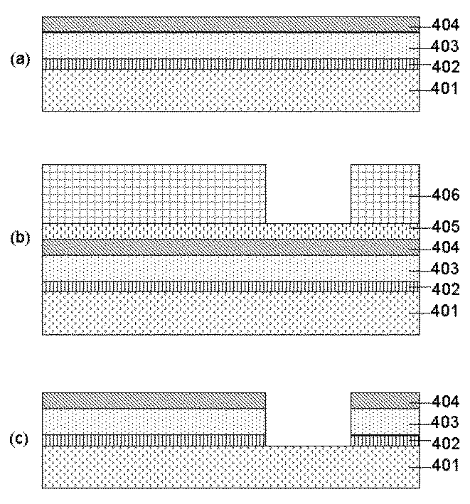
次に第1の実施の形態の半導体装置の製造方法を図4〜図7を参照して説明する。まず、トランジスタが形成された半導体基板を含む下層絶縁膜401上に、50nm〜100nmの膜厚の第0のシリコン炭化窒化膜402をプラズマCVD法により形成した。続いて、第1のL−Ox膜403の塗布・焼成を行ない、150nm〜350nmの膜厚に成膜した。その上に、第1のSiO2膜404を50nm〜200nmの膜厚にプラズマCVD法により成膜した(図4(a))。この構造体上に反射防止膜として第1のARC膜405を塗布した後に、最小L/S=0.14/0.14μmレベルのフォトリソグラフィー技術を用いパターニングされた第1のフォトレジストマスク406を形成した(図4(b))。
Next, a method of manufacturing the semiconductor device according to the first embodiment will be described with reference to FIGS. First, a 0-th silicon
これをマスクにして、第1のARC膜405、 第1のSiO2膜404、第1のL−Ox膜403をフロロカーボン系ガスを含んだエッチングガスにより順次エッチングし、第0のシリコン炭化窒化膜402上でストップさせるように第1の配線用溝を開口した。その後、酸素プラズマアッシングにより、フォトレジストマスクを剥離後、アミン系の有機剥離液などで残さ等を完全に除去した。その後、全面エッチバックにて、第1の配線用溝底部の第0のシリコン炭化窒化膜を除去した。さらに有機剥離液による洗浄で残さを除去した。この結果、第1の配線用溝パターンを形成した(図4(c))。
Using this as a mask, the
次に、スパッタ装置にてデガス処理、ArイオンによるRFエッチを行なった後に第1のバリアメタル膜としてTaN膜407を約10nm形成し、続いてTa膜408を20nmを溝内部(側壁および底面)を含めて基板(第1のSiO2膜404)表面に成膜した。真空を破ることなく、Cuシード膜(図示省略)を約100nm形成した。次にCuめっきにて、銅膜409を約600nm形成した(図5(a))。
Next, a
その後、縦型炉アニールにて200〜400℃で焼成を行った。次にメタルCMP技術を用い、溝以外のメタルを除去し溝内にCuが埋め込まれた第1Cu溝配線を形成した(図5(b))。次に、プラズマCVD装置により、50〜1000nmの第1のシリコン炭化窒化膜410を形成した。続いて、150〜350nmの第2のL−Ox膜411、さらに、50〜200nmの第2のSiO2膜412を順次成膜した。第1のビア形成のためにフォトリソグラフィー技術を用い、0.14μm径のビアのパターンとして第2のARC膜413上に第2のフォトレジストマスク414を形成した(図5(c))。
Thereafter, firing was performed at 200 to 400 ° C. by vertical furnace annealing. Next, using a metal CMP technique, a metal other than the groove was removed to form a first Cu groove wiring in which Cu was buried in the groove (FIG. 5B). Next, a first
これをマスクにして、第2のARC膜413、第2のSiO2膜412、第2のL−Ox膜411を順次エッチングし、第1のシリコン炭化窒化膜410上でエッチストップさせたビア用溝を開口した。次にフォトレジストマスクと第2のARC膜をプラズマアッシングにより除去し、有機剥離液で残渣を除去した。その後、ビア用溝底部の第1のシリコン炭化窒化膜410を除去し第1のCu溝配線との電気的な導通を採るため、全面エッチバックを行った。その後、有機剥離液を行って残渣を除去した。続いて、スパッタ装置にて、デガスを行なった後、ArイオンによるRFエッチを行なった後にビア用溝内部(側壁および底面)を含めて基板(第2のSiO2膜412)表面に第2のバリアメタル膜としてTaN膜415の膜厚約10nm形成に引き続きTa膜416を20nm形成し、真空を破ることなく、Cuシード膜(図示省略)を約100nm形成した。次にCuめっきにて、銅膜417を約300nm形成した。その後、縦型炉アニールにて200〜400℃で焼成を行った。次にメタルCMP技術を用い、ビア以外のメタルを除去し溝内にCuが埋め込まれたビアを形成した(図6(a))。
Using this as a mask, the
次に、プラズマCVD装置により、50〜100nmの第2のシリコン炭化窒化膜418を形成した。続いて、150〜350nmの第3のL−Ox膜419、さらに50〜200nmの第3のSiO2膜420を順次成膜した(図6(b))。
Next, a second
この構造体上に反射防止膜として第3のARC膜421を塗布後に、最小L/S=0.14/0.14μmレベルのフォトリソグラフィー技術を用いパターニングされた第3のフォトレジストマスク422を形成した(図7(a))。
After applying a
これをマスクにして、第3のARC膜421、第3のSiO2膜420、第3のL−Ox膜419をフロロカーボン系ガスを含むエッチングガスにより順次エッチングし、第2のシリコン炭化窒化膜418上でストップさせるように第2の配線用溝を開口した。その後、酸素プラズマアッシングにより、フォトレジストマスクを剥離後、アミン系の有機剥離液などで残さ等を完全に除去した。その後、全面エッチバックにて、第2の配線用溝底部の第2のシリコン炭化窒化膜418を除去した。さらに有機剥離液による洗浄で残さを除去した。続いて、スパッタ装置にて、デガスを行なった後、ArイオンによるRFエッチを行った後に第3のバリアメタル膜としてTaN膜423の膜厚約10nm形成に引き続きTa膜424を20nm形成し、真空を破ることなく、Cuシード膜(図示省略)を約100nm形成した。次にCuめっきにて、銅膜425を約600nm形成した。その後、縦型炉アニールにて200〜400℃で焼成を行った。次にメタルCMP技術を用い、溝以外のメタルを除去し溝内にCuが埋め込まれた第2Cu溝配線を形成した。次に、プラズマCVD装置により、50〜100nmの第3のシリコン炭化窒化膜426を形成した(図7(b))。
Using this as a mask, the
その後第3のシリコン炭化窒化膜426(図1の第3のシリコン炭化窒化膜120に相当)上に300〜500nmのSiO2層間絶縁膜121をプラズマCVD法により形成し、第3のシリコン炭化窒化膜426およびSiO2層間絶縁膜121にフォトリソグラフィー技術を用い第2Cu溝配線上に開口を設けるためのフォトレジストマスクを形成した。続いて露出したSiO2層間絶縁膜121および第3のシリコン炭化窒化膜426をエッチングして第2Cu溝配線とボンディングパッドとを接続するための開口部を形成した。フォトレジストマスク除去後スパッタリング法によりTiN膜122を100〜200nm,Al−Cu(0.5%)膜123を800〜1000nm、TiN膜124を50〜100nmを順次成膜した。続いて、フォトリソグラフィー技術を用いボンディングパッドを形成するためのフォトレジストマスクを形成し、エッチング工程によりボンディングパッドを形成後フォトレジストマスクを除去した。そして、ボンディングパッド上のTiN膜124を覆うようにSiO2膜125を100〜200nm、SiON膜126を100〜200nmをプラズマCVD法により順次形成し、フォトリソグラフィー技術によりボンディングパッド123上のSiON膜126およびSiO2膜125の所定領域を開口しボンディングパッドを露出させた。
Thereafter, an SiO 2
以上により、図1に示す2層配線構造を有する半導体装置が得られた。この2層配線構造を形成するにあたり、CMPでは剥がれは発生せず、また、測定した0.14μmスペースでの配線間容量は目標どおりの値を得られ、さらにビア抵抗も歩留まり劣化なく、かつビア抵抗の上昇が発生することもなかった。 Thus, the semiconductor device having the two-layer wiring structure shown in FIG. 1 was obtained. In forming this two-layer wiring structure, no peeling occurs by CMP, the measured inter-wiring capacitance in the 0.14 μm space can be obtained as desired, the via resistance does not deteriorate, and the via resistance does not deteriorate. No increase in resistance occurred.
さらに、本発明者の実験ではCu配線およびCuビア上に用いているシリコン炭化窒化膜の窒素濃度が吸湿のブロック性に対して大きな鍵であることを突き止めた。図8にシリコン炭化窒化膜中のRBS(ラザフォード後方散乱分光法:Backscattering Spectroscopy)で測定した窒素濃度を横軸、実施の形態1を用いた場合のライン/スペース=0.14/0.14μm間隔での配線間容量の値を縦軸とした両者の関係を示した。シリコン炭化窒化膜中の窒素濃度の上昇に伴い配線間容量は低下し、約10atm%(原子%)以上の窒素濃度では飽和している。窒素濃度が0の場合は10atm%以上の場合と比較し、15%程度配線間容量が大きいことが確認された。 Further, the inventors' experiments have found that the nitrogen concentration of the silicon carbonitride film used on the Cu wiring and the Cu via is a key to the blocking property of moisture absorption. FIG. 8 shows the nitrogen concentration measured by RBS (Backscattering Spectroscopy) in the silicon carbonitride film on the horizontal axis, and the line / space in the case of using the first embodiment = 0.14 / 0.14 μm interval. The relationship between the two values is shown with the value of the capacitance between wirings at the vertical axis as the vertical axis. As the nitrogen concentration in the silicon carbonitride film increases, the capacitance between wirings decreases, and is saturated at a nitrogen concentration of about 10 atm% (atomic%) or more. When the nitrogen concentration was 0, it was confirmed that the inter-wiring capacitance was larger by about 15% as compared with the case where the nitrogen concentration was 10 atm% or more.
また、図9に示すように、膜の組成で窒素濃度が約35atm%以上のシリコン炭化窒化膜はその膜単独の比誘電率が5.8以上と急激に値が上がってしまいそれ以下の5.0以下の領域での低誘電率化のメリットはなくなってきてしまう。以上より、シリコン炭化窒化膜の窒素濃度は10atm%以上35atm%未満であることが望ましく、膜質の安定性の点から15atm%以上30atm%以下であることがより望ましい。 Further, as shown in FIG. 9, the relative permittivity of the silicon oxynitride film having a nitrogen concentration of about 35 atm% or more in the composition of the film is sharply increased to 5.8 or more, and the value of the dielectric constant of the film is 5% or less. The advantage of lowering the dielectric constant in the region of 0.0 or less disappears. As described above, the nitrogen concentration of the silicon carbonitride film is preferably 10 atm% or more and less than 35 atm%, and more preferably 15 atm% or more and 30 atm% or less from the viewpoint of film quality stability.
シリコン炭化窒化膜中の窒素濃度以外の他の組成はSiが22〜27atm%、Cが20〜25atm%、Hが35〜45atm%の範囲の膜で特性が良好であることが確認されており、この範囲内では、上記の関係は成立するものと考えられる(H濃度以外はRBS、 HはHFS(水素前方散乱分析:Hydrogen Front Scattering Spectroscopy)で測定)。 It has been confirmed that the composition other than the nitrogen concentration in the silicon carbonitride film is good in a film in the range of 22 to 27 atm% of Si, 20 to 25 atm% of C, and 35 to 45 atm% of H. Within this range, it is considered that the above relationship is satisfied (RBS other than H concentration, H is measured by HFS (Hydrogen Front Scattering Spectroscopy)).
また、図10は下層のCu配線に対する耐性を示したものである。シリコン炭化窒化膜中の窒素濃度を横軸、第3の実施形態の場合のビアチェーン抵抗値を縦軸として両者の相関を示す。シリコン炭化窒化膜中の窒素濃度の上昇に伴い抵抗値は下がっていき、約10atm%以上の窒素濃度ではビアの抵抗値は飽和領域に入っていることが確認された。窒素濃度が0atm%の場合は、10atm%以上の場合と比較し、剥がれが発生してビアチェーンの歩留まりが悪く、ビアがオープンでないものの平均値では約30%抵抗値が高いことが確認された。 FIG. 10 shows the resistance to the lower Cu wiring. The horizontal axis represents the nitrogen concentration in the silicon carbonitride film, and the vertical axis represents the via chain resistance value in the third embodiment, and shows the correlation between the two. As the nitrogen concentration in the silicon carbonitride film increases, the resistance value decreases, and it is confirmed that the resistance value of the via enters the saturation region at a nitrogen concentration of about 10 atm% or more. In the case where the nitrogen concentration was 0 atm%, peeling occurred and the yield of the via chain was poor as compared with the case where the nitrogen concentration was 10 atm% or more, and it was confirmed that although the via was not open, the average value was about 30% higher in the average value. .
ここでは水素化ポリシロキサンを用いているが、SiO2層間絶縁膜を用いても配線間容量の上昇は明確に確認できなかったもののビア抵抗の上昇は確認でき、層間絶縁膜によらず、Cu配線上にシリコン炭化窒化膜がある場合膜中の窒素濃度が少なくなると信頼性は低下する傾向があることも確認された。シリコン炭化窒化膜中の窒素濃度以外の他の組成はSiが22〜27atm%、Cが20〜25atm%、Hが35〜45atm%の範囲の膜で特性が良好であることが確認されており、この範囲内では、上記の関係は成立するものと考えられる。 Here, hydrogenated polysiloxane is used. However, although the increase in the inter-wiring capacitance could not be clearly confirmed even when the SiO 2 interlayer insulating film was used, the increase in the via resistance could be confirmed. It was also confirmed that when a silicon carbonitride film was present on the wiring, the reliability tended to decrease as the nitrogen concentration in the film decreased. It has been confirmed that the composition other than the nitrogen concentration in the silicon carbonitride film is good in a film in the range of 22 to 27 atm% of Si, 20 to 25 atm% of C, and 35 to 45 atm% of H. It is considered that the above relationship is satisfied within this range.
また、低誘電率化の観点では、本絶縁膜中にさらに酸素が含まれている方が好ましい。Oが1atm%で、無しの場合と比較し比誘電率が0.2程度の低減できる。Oが5atm%未満であれば、上記配線間容量の上昇抑制効果に差がないことが確認できている。しかしながら、5atm%以上では上記効果は急激に低下するため、Oの含有量は5atm%未満とすることが好ましく、0.5atm%から2atm%の範囲とすることがさらに好ましい。なお、水素濃度について記載すると、水素が入っていることによりCu酸化膜の還元効果があり、Cu配線の酸化を防止できるという効果がある。水素濃度が35atm%未満の場合はCu酸化膜が形成されやすく、抵抗値は上昇する傾向になる。 From the viewpoint of lowering the dielectric constant, it is preferable that the present insulating film further contains oxygen. O is 1 atm%, and the relative dielectric constant can be reduced to about 0.2 as compared with the case without O. It has been confirmed that when O is less than 5 atm%, there is no difference in the effect of suppressing the increase in the capacitance between wirings. However, when the content is 5 atm% or more, the above effect is sharply reduced. Therefore, the O content is preferably less than 5 atm%, and more preferably in the range of 0.5 atm% to 2 atm%. In terms of hydrogen concentration, the presence of hydrogen has the effect of reducing the Cu oxide film and has the effect of preventing oxidation of the Cu wiring. When the hydrogen concentration is less than 35 atm%, a Cu oxide film is easily formed, and the resistance value tends to increase.
上記シリコン炭化窒化膜を有する効果がこの膜の有する吸湿のブロック性に起因することを確認するため、膜の吸湿ブロック性のテストを行った。サンプルとしては、全面成膜のPSG(Phospho-Silicate Glass)膜上にシリコン炭化窒化膜を成膜した。吸湿がブロックできない場合は、FTIRスペクトルを確認すれば、下層のPSG膜中のP=O結合の赤外線吸収ピークが消失する。膜の吸湿ブロック性のテストとして、PCT(Pressure Cooker Test)条件125℃、2気圧、湿度100%で保管した前後のFTIR(フーリエ変換赤外分光法:Fourier Transform Infrared Spectroscopy)スペクトルを比較した。 In order to confirm that the effect of having the silicon carbonitride film is due to the moisture blocking property of the film, a test of the moisture absorbing block property of the film was performed. As a sample, a silicon carbonitride film was formed on a PSG (Phospho-Silicate Glass) film formed on the entire surface. If moisture absorption cannot be blocked, the infrared absorption peak of the P = O bond in the lower PSG film disappears by checking the FTIR spectrum. As a test of the film's ability to block moisture absorption, FTIR (Fourier Transform Infrared Spectroscopy) spectra before and after storage under PCT (Pressure Cooker Test) conditions of 125 ° C., 2 atm, and 100% humidity were compared.
参考の為、図11に示すように、明らかに吸湿ブロック性がないプラズマCVD法によるSiO2膜をPSG膜上に成膜したサンプルのPCT前後のFTIRスペクトルを比較した。約1330cm−1の波数に存在するP=O結合はPCT前には確認されたが、PCT96時間経過後のFTIRスペクトルでは消失し、確認できなかった。すなわち、吸湿ブロック性は本方法で確認できることが確認できた。 For reference, as shown in FIG. 11, FTIR spectra before and after PCT of a sample in which an SiO 2 film was formed on a PSG film by a plasma CVD method having no apparent moisture absorption blocking property were compared. The P = O bond existing at a wavenumber of about 1330 cm −1 was confirmed before PCT, but disappeared in the FTIR spectrum after 96 hours of PCT, and could not be confirmed. That is, it was confirmed that the moisture absorption blocking property can be confirmed by this method.
この方法でPSG膜上にシリコン炭化窒化膜を成膜したサンプルを用い、窒素濃度をかえた場合の試験をおこなった。図12はSiC/PSG構造での、すなわち、窒素濃度=0atm%の場合のPCT前後のスペクトル比較である。PCT前に存在するP=O結合は96時間のPCT後では消失している。すなわち、吸湿のブロック性はない。また、図13にシリコン炭化窒化膜/PSG構造(上層がシリコン炭化窒化膜、下層がPSG)の結果を示す。このシリコン炭化窒化膜の窒素濃度は13.8atm%であった。このときにはPCT前に存在するP=O結合はPCT後でもほぼすべて残っていることが確認でき、すなわち、吸湿ブロック性が確認できた。 Using a sample in which a silicon carbonitride film was formed on a PSG film by this method, a test was performed when the nitrogen concentration was changed. FIG. 12 is a spectrum comparison before and after PCT in the SiC / PSG structure, that is, when the nitrogen concentration is 0 atm%. The P = O bonds present before PCT have disappeared after 96 hours of PCT. That is, there is no moisture absorption blocking property. FIG. 13 shows the results of a silicon carbonitride film / PSG structure (the upper layer is a silicon carbonitride film and the lower layer is PSG). The nitrogen concentration of this silicon carbonitride film was 13.8 atm%. At this time, it was confirmed that almost all P = O bonds existing before PCT remained even after PCT, that is, the moisture absorption blocking property was confirmed.
表1にシリコン炭化窒化膜中の窒素濃度とPCT後にP=O結合が存在するかの判定結果を示す。窒素濃度が10atm%では、P=O結合がほぼ残っておりこの領域では吸湿のブロック性はあると判断できる。また、約8atm%では、ややP=Oの結合のピークの減少はみられたが、存在することは確認できた。また、それ以下の窒素濃度の水準では、P=O結合はPCT後に確認できなかった。すなわち、吸湿ブロック性はない。 Table 1 shows the nitrogen concentration in the silicon carbonitride film and the results of determination as to whether or not P = O bonds exist after PCT. When the nitrogen concentration is 10 atm%, P = O bonds almost remain, and it can be determined that there is a moisture absorption blocking property in this region. At about 8 atm%, the peak of the P = O bond was slightly reduced, but it was confirmed that it was present. At a nitrogen concentration level lower than that, no P = O bond could be confirmed after PCT. That is, there is no moisture absorption blocking property.
この吸湿ブロック性と前記電気特性の結果は対応し、すなわち、シリコン炭化窒化膜の吸湿ブロック性が電気特性を支配していると推察できる。 The results of the moisture absorption blocking property and the electrical characteristics correspond to each other, that is, it can be inferred that the moisture absorption blocking property of the silicon carbonitride film controls the electrical properties.
次にバリアメタル膜と低誘電率膜である水素化ポリシロキサンとの関係を説明する。表2にバリアメタル膜として、Ta/TaN(上層がTa:20nm、下層がTaN:10nm)を使用した場合のTaNの窒素濃度とメタルCMPでのはがれの有無およびTaNスパッタ時のゴミ検査での欠陥数との関係を示した。 Next, the relationship between the barrier metal film and the hydrogenated polysiloxane, which is a low dielectric constant film, will be described. Table 2 shows that when Ta / TaN (Ta: 20 nm for the upper layer, TaN: 10 nm for the lower layer) is used as the barrier metal film, the nitrogen concentration of TaN, the presence or absence of peeling by metal CMP, and the dust inspection at the time of TaN sputtering. The relationship with the number of defects was shown.
TaNのXPS(X線光電子分光法:X-ray Photoelectron Spectroscopy)で求めた窒素濃度が約10atm%以上の膜では、第3の実施形態で行った場合では剥がれが発生しなかったが、それ以下ではCu膜のCMPで剥がれが発生した。特に5atm%以下の膜では、目視でも剥がれが確認できた。約8atm%程度では目視では確認できなかったものの、光学顕微鏡で剥がれが確認できた。ちなみに層間絶縁膜がSiO2の場合ではいずれの窒素濃度のTaNでも剥がれが発生していないことより、水素化ポリシロキサンの水素がTaNに吸蔵しているものと推定できる。また、TaNをスパッタしたときの8インチウエハ上でのゴミカウント数を示す。ゴミの粒径は0.18μm以上のものをカウントした。TaNの窒素濃度が40atm%未満のレベルでは20個以下であったが、40atm%を超えると20000個以上の個数を示し、オーバーフローした。 In a film having a nitrogen concentration of about 10 atm% or more obtained by TaN XPS (X-ray Photoelectron Spectroscopy), peeling did not occur in the case of the third embodiment, but not more than that. In this case, the Cu film was peeled off by CMP. In particular, in the case of a film of 5 atm% or less, peeling was confirmed visually. Although about 8 atm% could not be confirmed visually, peeling could be confirmed by an optical microscope. Incidentally, in the case where the interlayer insulating film is SiO 2 , it is presumed that hydrogen of the hydrogenated polysiloxane is occluded in TaN, since peeling does not occur in TaN of any nitrogen concentration. Also, the number of dust counts on an 8-inch wafer when TaN is sputtered is shown. Particles having a particle size of 0.18 μm or more were counted. When the nitrogen concentration of TaN was less than 40 atm%, the number was 20 or less, but when it exceeded 40 atm%, the number was 20,000 or more, and overflow occurred.
また表3にバリアメタルの構造による、0.14μm径の高さ0.4μmのビアへのCu埋設性およびメタルCMP時の剥がれの関係を示す。 Table 3 shows the relationship between the embedding property of Cu into a via having a diameter of 0.14 μm and a height of 0.4 μm and peeling during metal CMP, depending on the structure of the barrier metal.
Ta単層30nmの膜上に100nmのCuシード層を成膜し、その上に300nmのCuめっきを埋設し、加速試験として450℃で12時間過熱したときの埋設を確認したところ、埋設不良は確認できなかった。Ta(20nm)/TaN(10nm)の場合(その上のCuは同じ条件)でも問題はなかったが、30nmのTaN単層では埋設不良が確認された。この原因はCu膜の濡れ性の下地依存性で説明できる。Ta膜へのCu膜の濡れ性はよいが、TaNへのCu膜の濡れ性は悪い。これはCu濡れ性と窒素がなんらかの関係があると思われる。またビアCuのCMPでの剥がれは、TaN単層の場合と、Ta/TaNの積層の場合は問題がなかったが、Ta単層の場合は剥がれが確認された。この原因は水素化ポリシロキサンの水素が、Taに吸蔵し、メタルの脆弱が発生しているものと推定される。Taに窒素が含まれると水素の吸蔵が抑えられ、バリアメタル脆弱化が防止できると考えられる。 A 100-nm Cu seed layer was formed on a 30-nm Ta single layer, and a 300-nm Cu plating layer was buried thereon. As an accelerated test, embedding when overheating at 450 ° C. for 12 hours was confirmed. I could not confirm. Although there was no problem in the case of Ta (20 nm) / TaN (10 nm) (Cu on top of the same condition), a burying defect was confirmed in a TaN single layer of 30 nm. The cause can be explained by the dependence of the wettability of the Cu film on the underlayer. The wettability of the Cu film to the Ta film is good, but the wettability of the Cu film to TaN is poor. This seems to have some relationship between Cu wettability and nitrogen. There was no problem in the peeling of the via Cu by CMP in the case of the TaN single layer and in the case of the Ta / TaN lamination, but in the case of the Ta single layer, the peeling was confirmed. It is presumed that the cause of this is that hydrogen of the hydrogenated polysiloxane is occluded in Ta and the metal is brittle. It is considered that when nitrogen is contained in Ta, the occlusion of hydrogen is suppressed and barrier metal embrittlement can be prevented.
バリアメタル膜はTa/TaNの積層構造に限定されるものではない。層間絶縁膜としてSi−H結合を有する層間絶縁膜のHがバリアメタル膜に吸蔵しメタルの脆弱化をもたらさないような構成とすればよい。即ち、Si−H結合を有する層間絶縁膜と水素吸蔵性を有するバリアメタル膜を用いる場合、両者間に層間絶縁膜のHのバリアメタル膜への吸蔵を抑制する層を設ける構成とすればよい。水素吸蔵性を有するバリマタルとしては、Ta以外にTiが挙げられる。TaN同様TiNも水素の吸蔵が抑えられ、バリアメタル脆弱化が防止できると考えられる。したがって、Ta/TaN以外にTa/TiN、Ti/TaN、Ti/TiNの組合せも可能である。 The barrier metal film is not limited to the stacked structure of Ta / TaN. The interlayer insulating film may have a structure in which H of the interlayer insulating film having a Si—H bond is not absorbed into the barrier metal film and does not weaken the metal. That is, when an interlayer insulating film having a Si-H bond and a barrier metal film having a hydrogen absorbing property are used, a layer for suppressing occlusion of H of the interlayer insulating film into the barrier metal film may be provided therebetween. . Examples of barimatal having hydrogen storage properties include Ti in addition to Ta. It is considered that TiN, like TaN, suppresses the absorption of hydrogen and can prevent the barrier metal from becoming brittle. Therefore, a combination of Ta / TiN, Ti / TaN, and Ti / TiN other than Ta / TaN is also possible.
上記実施形態では、梯子型水素化ポリシロキサンであるL−Oxを低誘電率層間絶縁膜として使用した例を示したが、かご型の水素化ポリシロキサンの1種である籠型水素化シルセスキオキサンを用いてもよい。但し、梯子型水素化ポリシロキサンを用いた場合より水素吸蔵抑制層を介在させる効果はやや小さい。また比誘電率2.4のポーラス梯子型水素化ポリシロキサン(ポーラスL−Ox)を用いた場合も同等の効果が確認された。梯子型水素化ポリシロキサンまたはポーラス梯子型水素化ポリシロキサンであることが好ましい。また効果としては水素化ポリシロキサンよりも少ないがCVD法で形成した水素化オルガノポリシロキサン、即ち、Si−H結合とSi−CH3結合をともにもっている絶縁膜(この結合はFTIRスペクトルなどで確認できる)でもよい。たとえば商品名であれば、Black Diamond(商標名)、Coral(商標名)、Aurora(商標名)などでも同様な結果が得られる。塗布法で形成したMHSQなどでも同様な結果が得られた。上記効果の程度の差は、Si−CH3結合のHがSi−H結合のHよりも解離し難いことに基因すると考えられる。即ち、Si−H結合を多く有する絶縁膜材料を使用するほど水素吸蔵抑制層を介在させる効果は大きく認められた。 In the above embodiment, the example in which L-Ox, which is a ladder-type hydrogenated polysiloxane, is used as the low dielectric constant interlayer insulating film has been described. However, a cage-type hydrogenated silsesquide, which is one type of cage-type hydrogenated polysiloxane, is shown. Oxane may be used. However, the effect of interposing the hydrogen absorption suppressing layer is slightly smaller than when the ladder-type hydrogenated polysiloxane is used. The same effect was confirmed when a porous ladder-type hydrogenated polysiloxane (porous L-Ox) having a relative dielectric constant of 2.4 was used. It is preferably a ladder-type hydrogenated polysiloxane or a porous ladder-type hydrogenated polysiloxane. The effect is also lower than that of hydrogenated polysiloxane, but is a hydrogenated organopolysiloxane formed by a CVD method, that is, an insulating film having both a Si—H bond and a Si—CH 3 bond (this bond is confirmed by an FTIR spectrum or the like). Can be). For example, similar names can be obtained for Black Diamond (trade name), Coral (trade name), Aurora (trade name), and the like. Similar results were obtained with MHSQ and the like formed by the coating method. It is considered that the difference in the degree of the effect is due to the fact that H of the Si—CH 3 bond is less likely to dissociate than H of the Si—H bond. In other words, the effect of interposing the hydrogen absorption suppressing layer was larger as the insulating film material having more Si-H bonds was used.
本発明によれば、配線およびバリアメタル膜との良好な密着性を有するSi−H結合を有する低誘電率層間絶縁膜と好ましい組成のシリコン炭化窒化膜の組合せにより本発明の第1から第3の実施形態の9層配線構造の多層配線構造を10ヶ月かけて製造しても配線間容量が増加することはなかった。また、ビア抵抗が上昇することがなく、かつ膜剥がれも発生せずに製造できた。 According to the present invention, the first to third aspects of the present invention are realized by a combination of a low dielectric constant interlayer insulating film having a Si—H bond having good adhesion to a wiring and a barrier metal film and a silicon oxynitride film having a preferable composition. Even if the multilayer wiring structure of the nine-layer wiring structure of the embodiment was manufactured for 10 months, the capacitance between wirings did not increase. In addition, it was possible to manufacture without increasing the via resistance and without peeling off the film.
101・・・下地絶縁膜
102,108,114,120,202,208,213,219,302,308,311,317,402,410,418,426・・・シリコン炭化窒化膜
103,109,115,203,214,303,309,312,403,411,419・・・L−Ox膜
104,110,116,121,125,204,209,215,304,310,313,404,412,420,504,509,514,604,612,620・・・SiO2膜
105,111,117,205,210,216,305,314,407,415,423・・・TaN膜
106,112,118,206,211,217,306,315,408,416,424・・・Ta膜
107,113,119,207,211,218,307,316,409,417,425,506,511,516,609,617,624・・・Cu膜
122,124・・・TiN膜
123・・・Al−Cu膜
126・・・SiON膜
502,507,512,517,602,609,616,623・・・バリア絶縁膜503,508,513,603,611,619・・・低誘電率膜
505,510,515,607,615,623・・・バリアメタル膜
101 ... underlying insulating
Claims (23)
前記層間絶縁膜を加工する第2の工程と、
バリアメタル膜を成膜する第3の工程と、
Cuを主たる構成元素とする導電膜を成膜する第4の工程と、
前記導電膜上にシリコン炭化窒化膜を成膜する第5の工程と、
を含むことを特徴とする半導体装置の製造方法。 A first step of forming an interlayer insulating film having a Si—H bond on a semiconductor substrate;
A second step of processing the interlayer insulating film;
A third step of forming a barrier metal film;
A fourth step of forming a conductive film containing Cu as a main constituent element,
A fifth step of forming a silicon carbonitride film on the conductive film;
A method for manufacturing a semiconductor device, comprising:
前記第3の工程は、前記溝の側壁および底面にバリアメタル膜を成膜する工程であり、
前記第4の工程は、前記バリアメタルが成膜された溝内に前記導電膜を埋設する工程であり、
前記第5の工程は、前記層間絶縁膜および導電膜上にシリコン炭化窒化膜を成膜する工程であることを特徴とする請求項14記載の半導体装置の製造方法。 The second step is a step of processing a groove in the interlayer insulating film,
The third step is a step of forming a barrier metal film on a side wall and a bottom surface of the groove.
The fourth step is a step of burying the conductive film in a groove in which the barrier metal is formed,
The method according to claim 14, wherein the fifth step is a step of forming a silicon carbonitride film on the interlayer insulating film and the conductive film.
Priority Applications (3)
| Application Number | Priority Date | Filing Date | Title |
|---|---|---|---|
| JP2003420838A JP2004253780A (en) | 2003-01-31 | 2003-12-18 | Semiconductor device and its manufacturing method |
| US10/766,886 US20040183202A1 (en) | 2003-01-31 | 2004-01-30 | Semiconductor device having copper damascene interconnection and fabricating method thereof |
| US11/101,416 US20050179137A1 (en) | 2003-01-31 | 2005-04-08 | Semiconductor device having copper damascene interconnection and fabricating method thereof |
Applications Claiming Priority (2)
| Application Number | Priority Date | Filing Date | Title |
|---|---|---|---|
| JP2003024716 | 2003-01-31 | ||
| JP2003420838A JP2004253780A (en) | 2003-01-31 | 2003-12-18 | Semiconductor device and its manufacturing method |
Publications (1)
| Publication Number | Publication Date |
|---|---|
| JP2004253780A true JP2004253780A (en) | 2004-09-09 |
Family
ID=33032296
Family Applications (1)
| Application Number | Title | Priority Date | Filing Date |
|---|---|---|---|
| JP2003420838A Pending JP2004253780A (en) | 2003-01-31 | 2003-12-18 | Semiconductor device and its manufacturing method |
Country Status (1)
| Country | Link |
|---|---|
| JP (1) | JP2004253780A (en) |
Cited By (7)
| Publication number | Priority date | Publication date | Assignee | Title |
|---|---|---|---|---|
| JP2010267971A (en) * | 2009-05-13 | 2010-11-25 | Air Products & Chemicals Inc | Deposition of dielectric barriers using nitrogen-containing precursors |
| JP2012146909A (en) * | 2011-01-14 | 2012-08-02 | Renesas Electronics Corp | Semiconductor device and method for manufacturing the same |
| WO2015098812A1 (en) * | 2013-12-27 | 2015-07-02 | 富士フイルム株式会社 | Pattern formation method, method for manufacturing solid-state imaging element, and method for manufacturing color filter |
| KR20210036865A (en) * | 2018-04-05 | 2021-04-05 | 더 리서치 파운데이션 포 더 스테이트 유니버시티 오브 뉴욕 | Photonic structure optical signal transmission area fabrication |
| CN113257811A (en) * | 2020-02-11 | 2021-08-13 | 台湾积体电路制造股份有限公司 | Semiconductor device and method of forming the same |
| CN116364758A (en) * | 2023-03-30 | 2023-06-30 | 苏州龙驰半导体科技有限公司 | SiC MOS device |
| US12400975B2 (en) | 2021-06-24 | 2025-08-26 | Samsung Electronics Co., Ltd. | Interconnect structure and electronic device including the same |
Citations (3)
| Publication number | Priority date | Publication date | Assignee | Title |
|---|---|---|---|---|
| JP2000150517A (en) * | 1998-11-16 | 2000-05-30 | Hitachi Ltd | Semiconductor integrated circuit device and method of manufacturing the same |
| JP2001053077A (en) * | 1999-08-13 | 2001-02-23 | Hitachi Ltd | Semiconductor integrated circuit device and method of manufacturing the same |
| JP2002329780A (en) * | 2001-04-27 | 2002-11-15 | Hitachi Ltd | Semiconductor device manufacturing method and semiconductor device |
-
2003
- 2003-12-18 JP JP2003420838A patent/JP2004253780A/en active Pending
Patent Citations (3)
| Publication number | Priority date | Publication date | Assignee | Title |
|---|---|---|---|---|
| JP2000150517A (en) * | 1998-11-16 | 2000-05-30 | Hitachi Ltd | Semiconductor integrated circuit device and method of manufacturing the same |
| JP2001053077A (en) * | 1999-08-13 | 2001-02-23 | Hitachi Ltd | Semiconductor integrated circuit device and method of manufacturing the same |
| JP2002329780A (en) * | 2001-04-27 | 2002-11-15 | Hitachi Ltd | Semiconductor device manufacturing method and semiconductor device |
Cited By (12)
| Publication number | Priority date | Publication date | Assignee | Title |
|---|---|---|---|---|
| JP2010267971A (en) * | 2009-05-13 | 2010-11-25 | Air Products & Chemicals Inc | Deposition of dielectric barriers using nitrogen-containing precursors |
| US8889235B2 (en) | 2009-05-13 | 2014-11-18 | Air Products And Chemicals, Inc. | Dielectric barrier deposition using nitrogen containing precursor |
| JP2012146909A (en) * | 2011-01-14 | 2012-08-02 | Renesas Electronics Corp | Semiconductor device and method for manufacturing the same |
| WO2015098812A1 (en) * | 2013-12-27 | 2015-07-02 | 富士フイルム株式会社 | Pattern formation method, method for manufacturing solid-state imaging element, and method for manufacturing color filter |
| KR20210036865A (en) * | 2018-04-05 | 2021-04-05 | 더 리서치 파운데이션 포 더 스테이트 유니버시티 오브 뉴욕 | Photonic structure optical signal transmission area fabrication |
| JP2021519948A (en) * | 2018-04-05 | 2021-08-12 | ザ リサーチ ファンデーション フォー ザ ステート ユニバーシティ オブ ニューヨーク | Fabrication of photonics structure optical signal transmission region |
| US11635568B2 (en) | 2018-04-05 | 2023-04-25 | The Research Foundation For The State University Of New York | Photonics light signal transmission |
| KR102806076B1 (en) * | 2018-04-05 | 2025-05-09 | 더 리서치 파운데이션 포 더 스테이트 유니버시티 오브 뉴욕 | Manufacturing of photonic structures for optical signal transmission areas |
| CN113257811A (en) * | 2020-02-11 | 2021-08-13 | 台湾积体电路制造股份有限公司 | Semiconductor device and method of forming the same |
| US12400975B2 (en) | 2021-06-24 | 2025-08-26 | Samsung Electronics Co., Ltd. | Interconnect structure and electronic device including the same |
| CN116364758A (en) * | 2023-03-30 | 2023-06-30 | 苏州龙驰半导体科技有限公司 | SiC MOS device |
| CN116364758B (en) * | 2023-03-30 | 2023-11-14 | 苏州龙驰半导体科技有限公司 | SiC MOS devices |
Similar Documents
| Publication | Publication Date | Title |
|---|---|---|
| US7615498B2 (en) | Method of manufacturing a semiconductor device | |
| US20050179137A1 (en) | Semiconductor device having copper damascene interconnection and fabricating method thereof | |
| US7749892B2 (en) | Embedded nano UV blocking and diffusion barrier for improved reliability of copper/ultra low K interlevel dielectric electronic devices | |
| JP4086673B2 (en) | Semiconductor device and manufacturing method thereof | |
| JP5482881B2 (en) | Semiconductor device and manufacturing method of semiconductor device | |
| US10510588B2 (en) | Interconnection structure and manufacturing method thereof | |
| US20070059919A1 (en) | Method of manufacturing semiconductor device | |
| US20100196806A1 (en) | Structures and methods for low-k or ultra low-k interlayer dielectric pattern transfer | |
| JP4746829B2 (en) | Semiconductor device and manufacturing method thereof | |
| JP5380838B2 (en) | Manufacturing method of semiconductor device | |
| US7230337B2 (en) | Semiconductor device including ladder-shaped siloxane hydride and method for manufacturing same | |
| US7253524B2 (en) | Copper interconnects | |
| JP2004193544A (en) | Semiconductor device and method of manufacturing same | |
| CN1989608A (en) | Semiconductor device and semiconductor device manufacturing method | |
| US8390135B2 (en) | Semiconductor device | |
| US20060118955A1 (en) | Robust copper interconnection structure and fabrication method thereof | |
| JP2004253780A (en) | Semiconductor device and its manufacturing method | |
| KR100562630B1 (en) | Method of forming copper interconnects in integrated circuits | |
| US7579277B2 (en) | Semiconductor device and method for fabricating the same | |
| JP5200436B2 (en) | Manufacturing method of semiconductor device | |
| CN108573912B (en) | Semiconductor structure and method of forming the same | |
| JP4160489B2 (en) | Manufacturing method of semiconductor device | |
| JP2004253781A (en) | Semiconductor device and its manufacturing method | |
| CN100550366C (en) | Semiconductor chip | |
| JP2004296620A (en) | Process for fabricating semiconductor device |
Legal Events
| Date | Code | Title | Description |
|---|---|---|---|
| A621 | Written request for application examination |
Free format text: JAPANESE INTERMEDIATE CODE: A621 Effective date: 20061102 |
|
| RD01 | Notification of change of attorney |
Free format text: JAPANESE INTERMEDIATE CODE: A7421 Effective date: 20070704 |
|
| A977 | Report on retrieval |
Free format text: JAPANESE INTERMEDIATE CODE: A971007 Effective date: 20090129 |
|
| RD01 | Notification of change of attorney |
Free format text: JAPANESE INTERMEDIATE CODE: A7421 Effective date: 20100426 |
|
| A131 | Notification of reasons for refusal |
Free format text: JAPANESE INTERMEDIATE CODE: A131 Effective date: 20100727 |
|
| A02 | Decision of refusal |
Free format text: JAPANESE INTERMEDIATE CODE: A02 Effective date: 20101124 |