JP2004207687A - Semiconductor manufacturing apparatus and semiconductor manufacturing method using the same - Google Patents
Semiconductor manufacturing apparatus and semiconductor manufacturing method using the same Download PDFInfo
- Publication number
- JP2004207687A JP2004207687A JP2003365002A JP2003365002A JP2004207687A JP 2004207687 A JP2004207687 A JP 2004207687A JP 2003365002 A JP2003365002 A JP 2003365002A JP 2003365002 A JP2003365002 A JP 2003365002A JP 2004207687 A JP2004207687 A JP 2004207687A
- Authority
- JP
- Japan
- Prior art keywords
- temperature
- wafer
- signal
- chamber
- semiconductor manufacturing
- Prior art date
- Legal status (The legal status is an assumption and is not a legal conclusion. Google has not performed a legal analysis and makes no representation as to the accuracy of the status listed.)
- Pending
Links
Images


Classifications
-
- H10P72/0602—
-
- C—CHEMISTRY; METALLURGY
- C23—COATING METALLIC MATERIAL; COATING MATERIAL WITH METALLIC MATERIAL; CHEMICAL SURFACE TREATMENT; DIFFUSION TREATMENT OF METALLIC MATERIAL; COATING BY VACUUM EVAPORATION, BY SPUTTERING, BY ION IMPLANTATION OR BY CHEMICAL VAPOUR DEPOSITION, IN GENERAL; INHIBITING CORROSION OF METALLIC MATERIAL OR INCRUSTATION IN GENERAL
- C23C—COATING METALLIC MATERIAL; COATING MATERIAL WITH METALLIC MATERIAL; SURFACE TREATMENT OF METALLIC MATERIAL BY DIFFUSION INTO THE SURFACE, BY CHEMICAL CONVERSION OR SUBSTITUTION; COATING BY VACUUM EVAPORATION, BY SPUTTERING, BY ION IMPLANTATION OR BY CHEMICAL VAPOUR DEPOSITION, IN GENERAL
- C23C16/00—Chemical coating by decomposition of gaseous compounds, without leaving reaction products of surface material in the coating, i.e. chemical vapour deposition [CVD] processes
- C23C16/44—Chemical coating by decomposition of gaseous compounds, without leaving reaction products of surface material in the coating, i.e. chemical vapour deposition [CVD] processes characterised by the method of coating
- C23C16/458—Chemical coating by decomposition of gaseous compounds, without leaving reaction products of surface material in the coating, i.e. chemical vapour deposition [CVD] processes characterised by the method of coating characterised by the method used for supporting substrates in the reaction chamber
- C23C16/4582—Rigid and flat substrates, e.g. plates or discs
- C23C16/4583—Rigid and flat substrates, e.g. plates or discs the substrate being supported substantially horizontally
- C23C16/4584—Rigid and flat substrates, e.g. plates or discs the substrate being supported substantially horizontally the substrate being rotated
-
- C—CHEMISTRY; METALLURGY
- C23—COATING METALLIC MATERIAL; COATING MATERIAL WITH METALLIC MATERIAL; CHEMICAL SURFACE TREATMENT; DIFFUSION TREATMENT OF METALLIC MATERIAL; COATING BY VACUUM EVAPORATION, BY SPUTTERING, BY ION IMPLANTATION OR BY CHEMICAL VAPOUR DEPOSITION, IN GENERAL; INHIBITING CORROSION OF METALLIC MATERIAL OR INCRUSTATION IN GENERAL
- C23C—COATING METALLIC MATERIAL; COATING MATERIAL WITH METALLIC MATERIAL; SURFACE TREATMENT OF METALLIC MATERIAL BY DIFFUSION INTO THE SURFACE, BY CHEMICAL CONVERSION OR SUBSTITUTION; COATING BY VACUUM EVAPORATION, BY SPUTTERING, BY ION IMPLANTATION OR BY CHEMICAL VAPOUR DEPOSITION, IN GENERAL
- C23C16/00—Chemical coating by decomposition of gaseous compounds, without leaving reaction products of surface material in the coating, i.e. chemical vapour deposition [CVD] processes
- C23C16/44—Chemical coating by decomposition of gaseous compounds, without leaving reaction products of surface material in the coating, i.e. chemical vapour deposition [CVD] processes characterised by the method of coating
- C23C16/46—Chemical coating by decomposition of gaseous compounds, without leaving reaction products of surface material in the coating, i.e. chemical vapour deposition [CVD] processes characterised by the method of coating characterised by the method used for heating the substrate
-
- C—CHEMISTRY; METALLURGY
- C23—COATING METALLIC MATERIAL; COATING MATERIAL WITH METALLIC MATERIAL; CHEMICAL SURFACE TREATMENT; DIFFUSION TREATMENT OF METALLIC MATERIAL; COATING BY VACUUM EVAPORATION, BY SPUTTERING, BY ION IMPLANTATION OR BY CHEMICAL VAPOUR DEPOSITION, IN GENERAL; INHIBITING CORROSION OF METALLIC MATERIAL OR INCRUSTATION IN GENERAL
- C23C—COATING METALLIC MATERIAL; COATING MATERIAL WITH METALLIC MATERIAL; SURFACE TREATMENT OF METALLIC MATERIAL BY DIFFUSION INTO THE SURFACE, BY CHEMICAL CONVERSION OR SUBSTITUTION; COATING BY VACUUM EVAPORATION, BY SPUTTERING, BY ION IMPLANTATION OR BY CHEMICAL VAPOUR DEPOSITION, IN GENERAL
- C23C16/00—Chemical coating by decomposition of gaseous compounds, without leaving reaction products of surface material in the coating, i.e. chemical vapour deposition [CVD] processes
- C23C16/44—Chemical coating by decomposition of gaseous compounds, without leaving reaction products of surface material in the coating, i.e. chemical vapour deposition [CVD] processes characterised by the method of coating
- C23C16/52—Controlling or regulating the coating process
Landscapes
- Chemical & Material Sciences (AREA)
- General Chemical & Material Sciences (AREA)
- Chemical Kinetics & Catalysis (AREA)
- Engineering & Computer Science (AREA)
- Materials Engineering (AREA)
- Mechanical Engineering (AREA)
- Metallurgy (AREA)
- Organic Chemistry (AREA)
- Chemical Vapour Deposition (AREA)
- Drying Of Semiconductors (AREA)
Abstract
Description
この発明は、半導体製造装置に関し、とくにCVD装置,蒸着装置,ドライエッチング装置又はイオン注入装置のような半導体製造装置に関する。 The present invention relates to a semiconductor manufacturing apparatus, and particularly to a semiconductor manufacturing apparatus such as a CVD apparatus, a vapor deposition apparatus, a dry etching apparatus, or an ion implantation apparatus.
この発明に関連する背景技術としては、冷却手段を有する下部電極にウェハを載置し、ウェハのプラズマエッチングを行う半導体製造装置において、エッチングチャンバー壁にチャンバー内のウェハに向けて埋め込まれた赤外線温度測定器と、この温度測定器からの信号により冷媒温度を制御しウェハ温度を設定値に保つための温度コントローラとを有し、赤外温度測定器によってウェハ温度を非接触で測定するようにした半導体製造装置が知られている(例えば、特許文献1参照)。
CVD装置,蒸着装置,ドライエッチング装置又はイオン注入装置のような半導体製造装置においては、成膜の均一性を図るために、通常、ウェハを回転テーブル上に載置してヒータから受ける熱量を均一化するようにしている。また、このような装置では、ウェハの温度が成膜特性を決定する重要な制御因子であり、ウェハ温度を測定しヒータの出力を制御することによって安定した成膜特性を得ることができる。ところで、ウェハ温度を従来のように赤外線温度測定器を用いて非接触で測定すると、測定器の赤外線を受け入れる窓が曇ったり、窓に塵埃が付着することが見受けられ、常に正確にウェハ温度を測定することが難しいという問題があった。 2. Description of the Related Art In a semiconductor manufacturing apparatus such as a CVD apparatus, a vapor deposition apparatus, a dry etching apparatus, or an ion implantation apparatus, a wafer is usually placed on a rotary table and the amount of heat received from a heater is made uniform in order to achieve uniform film formation. It is trying to be. In such an apparatus, the temperature of the wafer is an important control factor for determining the film forming characteristics, and stable film forming characteristics can be obtained by measuring the wafer temperature and controlling the output of the heater. By the way, when the wafer temperature is measured in a non-contact manner using an infrared temperature measuring device as in the past, it is observed that the window for receiving the infrared light of the measuring device becomes cloudy or dust adheres to the window. There was a problem that it was difficult to measure.
この発明はこのような事情を考慮してなされたもので、回転テーブルに付設した温度検知素子によりウェハ温度を直接接触して測定し、それによって、ヒータ出力を精度よく制御することが可能な半導体製造装置およびそれを用いた半導体製造装置を提供するものである。 The present invention has been made in view of such circumstances, and a semiconductor device capable of accurately controlling a heater output by directly measuring a wafer temperature by a temperature detection element attached to a rotary table. A manufacturing apparatus and a semiconductor manufacturing apparatus using the same are provided.
この発明は、ウェハを載置して回転する回転テーブルと、回転テーブルを収容するチャンバーと、ウェハを加熱するためにチャンバー内に設けられたヒータと、ウェハに接触してウェハの温度を検知する温度検知素子と、温度検知素子の出力を測定温度を表わす信号に変換して出力する温度測定部と、温度測定部の出力をチャンバーの外から認識できる信号に変換して出力する信号生成部を備え、温度検知素子と温度測定部と信号生成部が回転テーブルに付設されてなる半導体製造装置を提供するものである。 According to the present invention, a rotary table for mounting and rotating a wafer, a chamber for housing the rotary table, a heater provided in the chamber for heating the wafer, and detecting a temperature of the wafer by contacting the wafer A temperature detecting element, a temperature measuring section for converting the output of the temperature detecting element into a signal representing the measured temperature and outputting the signal, and a signal generating section for converting the output of the temperature measuring section to a signal recognizable from outside the chamber and outputting the signal. It is an object of the present invention to provide a semiconductor manufacturing apparatus provided with a temperature detecting element, a temperature measuring section, and a signal generating section attached to a turntable.
この発明によれば、回転テーブルに付設した温度検知素子によりウェハ温度を検知し、検知されたウェハ温度がチャンバー外から認識できる信号に変換されて出力されるので、チャンバー外部でその信号を認識してヒータの出力を精度よく制御することができ、ウェハ温度を正しく管理することが可能となる。 According to the present invention, the wafer temperature is detected by the temperature detecting element attached to the rotary table, and the detected wafer temperature is converted into a signal recognizable from outside the chamber and output, so that the signal is recognized outside the chamber. As a result, the output of the heater can be accurately controlled, and the wafer temperature can be correctly managed.
この発明の半導体製造装置の特徴は、ウェハを載置して回転する回転テーブルと、回転テーブルを収容するチャンバーと、ウェハを加熱するためにチャンバー内に設けられたヒータと、ウェハの温度を検知する温度検知素子と、温度検知素子の出力を測定温度を表わ
す信号に変換して出力する温度測定部と、温度測定部の出力をチャンバーの外から認識できる信号に変換して出力する信号生成部を備え、温度検知素子と温度測定部と信号生成部が回転テーブルに付設されてなる点にある。
The features of the semiconductor manufacturing apparatus of the present invention include a rotating table on which a wafer is mounted and rotated, a chamber for accommodating the rotating table, a heater provided in the chamber for heating the wafer, and detection of the temperature of the wafer. Temperature detecting element, a temperature measuring unit for converting the output of the temperature detecting element into a signal representing the measured temperature and outputting the signal, and a signal generating unit for converting the output of the temperature measuring unit to a signal recognizable from outside the chamber and outputting the signal. And a temperature detecting element, a temperature measuring unit, and a signal generating unit are attached to the turntable.
この発明において、ウェハとは半導体の製造に一般的に用いられる高純度のSiウェハや、InPウェハなどを意味する。回転テーブルは、例えば、複数のウェハを円周上に配列して載置可能なディスクと、ディスクを回転可能に支持するシャフトと、シャフトに機械的に結合してディスクを回転させる駆動源から構成される。 In the present invention, a wafer means a high-purity Si wafer, an InP wafer, or the like generally used in the manufacture of semiconductors. The rotating table includes, for example, a disk on which a plurality of wafers can be arranged on a circumference and mounted thereon, a shaft for rotatably supporting the disk, and a drive source for mechanically coupling the shaft to rotate the disk. Is done.
この発明における温度検知素子とは、熱電対や測温抵抗体のような素子であり、測定温度範囲により適宜選択される。つまり、1000℃以下ではK熱電対、500℃以下では測温抵抗体を用いることが好ましい。
また、この発明における温度測定部は、熱電対を温度検知素子として用いる場合には、例えば、冷接点補償回路,リニアライザおよび直流増幅器などから構成される。
The temperature detecting element in the present invention is an element such as a thermocouple or a resistance thermometer, and is appropriately selected according to a measurement temperature range. That is, it is preferable to use a K thermocouple at a temperature of 1000 ° C. or less and a resistance temperature detector at a temperature of 500 ° C. or less.
In the case where a thermocouple is used as a temperature detecting element, the temperature measuring unit according to the present invention includes, for example, a cold junction compensation circuit, a linearizer, and a DC amplifier.
温度測定部の出力をチャンバーの外から認識できる信号に変換して出力する信号生成部には、温度測定部の出力を、例えばアナログ変調又はデジタル変調して電波で発信する無線送信器や、赤外線信号に変換して発信する赤外線送信器や、温度測定部の出力(温度)を対応する色や記号に変換して表示する表示装置、あるいは温度測定部の出力を温度プロファイルデータとしてフラッシュメモリに記憶させる記憶装置などを用いることができる。 The signal generation unit converts the output of the temperature measurement unit into a signal that can be recognized from outside the chamber and outputs the signal. An infrared transmitter that converts the signal into a signal and transmits it, a display device that converts the output (temperature) of the temperature measurement unit to the corresponding color or symbol and displays it, or stores the output of the temperature measurement unit in the flash memory as temperature profile data For example, a storage device that allows the storage device to be used can be used.
信号生成部が上記無線送信器の場合には、チャンバー外に受信器とヒータ制御部をさらに設け、受信信号に基づいてヒータ出力をフィードバック制御すればよい。
信号生成部が赤外線送信器の場合には、チャンバー外に赤外線受信器とヒータ制御部をさらに設け、受信した赤外線信号に基づいてヒータ出力をフィードバック制御すればよい。
信号生成部が表示素子の場合には、使用者が表示内容を認識し、それに基づいてヒータ出力を手動制御することもできる。
When the signal generator is the wireless transmitter, a receiver and a heater controller may be further provided outside the chamber, and the heater output may be feedback-controlled based on the received signal.
When the signal generator is an infrared transmitter, an infrared receiver and a heater controller may be further provided outside the chamber, and the heater output may be feedback-controlled based on the received infrared signal.
When the signal generation unit is a display element, the user can recognize the display content and manually control the heater output based on the display content.
また、信号生成部が温度測定部の出力を格納する着脱可能なフラッシュメモリのような記憶装置である場合は、加熱処理終了後に記憶装置をチャンバー外へ取り出し温度プロファイルを読み出して、ヒータの温度設定プログラムを修正するようにしてもよい。
着脱可能な記憶装置として、磁気ディスクの一種であるマイクロドライブを用いることも可能である。この場合、フラッシュメモリに比べメモリ容量が大きいので、より多段階の温度プログラム管理や、多数の温度検知素子を配した半導体製造装置内の温度勾配管理など複雑な制御を必要とする製造装置に最適なシステムを構築することが可能となる。
この発明の半導体製造装置は、温度測定部および信号生成部を冷却するための冷却部をさらに備えることが好ましい。
なお、温度測定部や信号生成部は駆動電源(例えば電池やバッテリー)を内蔵することができる。
When the signal generation unit is a storage device such as a removable flash memory for storing the output of the temperature measurement unit, the storage device is taken out of the chamber after the completion of the heating process, and the temperature profile is read to set the temperature of the heater. The program may be modified.
As a removable storage device, a microdrive, which is a type of magnetic disk, can be used. In this case, since the memory capacity is larger than that of flash memory, it is most suitable for manufacturing equipment that requires complicated control such as multi-step temperature program management and temperature gradient management in semiconductor manufacturing equipment with many temperature sensing elements. It is possible to construct a simple system.
It is preferable that the semiconductor manufacturing apparatus of the present invention further includes a cooling unit for cooling the temperature measurement unit and the signal generation unit.
Note that the temperature measurement unit and the signal generation unit can incorporate a drive power supply (for example, a battery or a battery).
また、チャンバー内に設けられるヒータは、ウェハを600〜800℃まで加熱する能力を有することが好ましく、それには、抵抗発熱体を好適に用いることができる。抵抗発熱体としては、金属発熱体、例えば、Fe−Cr−Al合金(フェライト系),Ni−Cr−Fe合金(オーステナイト系)および白金,タングステン(純金属系)などや、非金属発熱体、例えばSiC,MoSi2,LaCrO3およびグラファイトなどが挙げられる。
また、チャンバーは、半導体の製造工程に応じて必要な材料ガスを導入する導入口を備えることが好ましい。
Further, the heater provided in the chamber preferably has a capability of heating the wafer to 600 to 800 ° C., and for this, a resistance heating element can be suitably used. Examples of the resistance heating element include metal heating elements such as Fe-Cr-Al alloy (ferrite-based), Ni-Cr-Fe alloy (austenite-based), platinum and tungsten (pure metal-based), and non-metallic heating elements. For example, SiC, MoSi 2 , LaCrO 3, graphite and the like can be mentioned.
Further, it is preferable that the chamber be provided with an inlet for introducing a necessary material gas in accordance with a semiconductor manufacturing process.
この発明は、別の観点から、前記の半導体製造装置を使用し、回転テーブルにウェハを載置し、ヒータによりウェハを加熱し、チャンバー内に材料ガスを供給し、信号生成部の出力信号をチャンバーの外部から認識してヒータ出力を制御しながら半導体を製造する工程からなる半導体製造方法を提供するものである。 According to another aspect of the present invention, a wafer is placed on a rotary table, a wafer is heated by a heater, a material gas is supplied into a chamber, and an output signal of a signal generation unit is used. An object of the present invention is to provide a semiconductor manufacturing method including a step of manufacturing a semiconductor while controlling a heater output by recognizing the semiconductor from outside the chamber.
実施例
以下、図面に示す実施例に基づいてこの発明を詳述する。これによってこの発明が限定されるものではない。
第1実施例
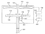
図1はIn系材料を用いるMOCVD装置の第1実施例を示す構成説明図である。
同図に示すように、円筒形のチャンバー104は、回転ディスク109を収容し、回転ディスク109はその上面に複数のウェハ101を搭載している。回転ディスク109はその中心を下方から中空シャフト110によって水平に支持され、中空シャフト110は図示しないモータに機械的に接続され、そのモータによって回転ディスク109が水平に矢印A方向に回転するようになっている。
Embodiments Hereinafter, the present invention will be described in detail based on embodiments shown in the drawings. This does not limit the present invention.
First Embodiment FIG. 1 is a structural explanatory view showing a first embodiment of a MOCVD apparatus using an In-based material.
As shown in the figure, a
また、チャンバー104は内部を外部から観察できるように周壁の少なくとも一部が透明になっている。回転ディスク109には熱電対106が埋設され、図2に示すように、その先端301は、ウェハ101の裏面に近接又は接触するようにディスク109の表面から突出して設置されている。
Further, at least a part of the peripheral wall of the
ところで、In系材料は分解しやすい特性を有するため、材料ガス導入口105から導入されるIn系ガスは、なるべくウェハ101の直近で分解させる必要がある。従って、回転ディスク109の表面中央部に導入される材料ガスの温度上昇を抑制するために、中空シャフト110内部に冷却水201を循環させ回転ディスク109の中央部を裏面から冷却するようにしている。
Incidentally, since the In-based material has a characteristic of being easily decomposed, the In-based gas introduced from the
熱電対106の起動力を測定温度に比例する温度データに変換する温度測定部107と、測定部107からの温度データを表示データに変換して測定温度を表示する表示部400とが、回転ディスク109の下側の中空シャフト110の近傍に設置され、冷却水201により冷却されるようになっている。なお、温度測定部107と表示部400は内蔵する電池で駆動する。
The rotating disk includes a
また、抵抗発熱体からなるヒータ103が、チャンバー104内の天井近傍に設置され、チャンバー104の外部に設けられたヒータ電源108に電気的に接続されている。ヒータ電源108は手動式コントローラ111に接続され、使用者がコントローラ111を操作することにより、ヒータ103の出力を制御できるようになっている。さらに、チャンバー104の天井の中央には、材料ガス導入口105が設けられている。
Further, a
なお、表示部400は、LCDやLED表示装置によって構成される。このような構成において、ヒータ電源108が駆動されると、チャンバー104内はヒータ103により加熱される。そして、表示装置400の表示するウェハ101の温度が約600℃になると、回転ディスク109が回転し、In材料ガス、例えばトリメチルインジウム(TMIn)ガスが所定時間だけ材料ガス導入口105からチャンバー104内へ導入され、InPなどの薄膜がウェハ101上に成膜される。
Note that the
この成膜工程中において、使用者はチャンバー104の側壁の透明部分を介して表示部400の表示内容を観察しながら、コントローラ111を手動操作して、ウェハ101の温度が所定の温度プロファイルに従って変化するように管理する。これによって、所望の
成膜特性を有するIn材料膜を得ることができる。
During this film forming process, the user manually operates the
第2実施例
図3はこの発明の第2実施例のMOCVD装置を示す構成説明図である。
図3に示すMOCVD装置は、図1に示す表示部400を無線送信器401に置換し、図1に示す手動式コントローラ109を無線受信器402とヒータ制御部202に置換したものであり、その他の構成は第1実施例の装置と同等である。
送信器401は温度測定部107から出力される温度データを符号化し、コードレス電話用の周波数でデジタル変調して受信器402へ無線送信するように構成されている。受信器402は、送信器401から受信した電波を検波しさらに複合化して制御部202へ出力するように構成される。
Second Embodiment FIG. 3 is a structural explanatory view showing a MOCVD apparatus according to a second embodiment of the present invention.
The MOCVD apparatus shown in FIG. 3 replaces the
The
制御部202はCPU,ROM,RAMからなるマイクロコンピュータで構成され、受信器402の出力、つまりウェハ101の温度データを受けて、RAMに予め格納されている設定温度プロファイルと、ウェハ101の温度データとが一致するように、ヒータ電源108を介してヒータ103の出力をフィードバック制御する。これによって、ウェハ101の温度が所定の温度プロファイルに基づいて管理される。
The
第3実施例
図4はこの発明の第3実施例のMOCVD装置を示す構成説明図である。
図4に示すMOCVD装置は、図3に示す送信器401を記憶部403に置換し、受信器402をメモリ読み出し装置404に置換したものであり、その他の構成は第2実施例と同等である。なお、記憶部403は、フラッシュメモリとしてのメモリカードを離脱可能に収容し温度測定部107の出力する温度データをそのメモリカードに記録できるようになっている。
Third Embodiment FIG. 4 is a structural explanatory view showing a MOCVD apparatus according to a third embodiment of the present invention.
The MOCVD apparatus shown in FIG. 4 replaces the
このような構成において、第1実施例と同様にして成膜工程を実行すると、ヒータ制御部202はRAMに予め格納している温度プロファイルに従ってヒータ電源108を介してヒータ103の出力をオープンループ制御する。
そして、ウェハ101の実測温度プロファイルが記憶部403においてメモリカードに記憶される。そして、成膜工程終了後に、使用者は記憶部403からメモリカードを取り出し、メモリ読み出し装置404に装填する。メモリ読み出し装置404はメモリカードから実測温度プロファイルを読み出す。制御部202はRAMに設定されている温度プロファイルと実測温度プロファイルを比較し、両者が一致するように、RAMに書き込まれているヒータ出力制御プログラムを修正する。これをくり返すことによって、ウェハ101の温度が所定の温度プロファイルに基づいて管理される。
In such a configuration, when the film forming process is performed in the same manner as in the first embodiment, the
Then, the measured temperature profile of the
101 ウェハ
103 ヒータ
104 チャンバー
105 材料ガス導入口
106 熱電対
107 温度測定部
108 ヒータ電源
109 回転ディスク
110 中空シャフト
111 手動式コントローラ
201 冷却水
301 先端
400 表示部
101
Claims (8)
Using the semiconductor manufacturing apparatus according to claim 1, a wafer is placed on a rotary table, the wafer is heated by a heater, a material gas is supplied into the chamber, and an output signal of the signal generation unit is recognized from outside the chamber. A semiconductor manufacturing method comprising the steps of manufacturing a semiconductor while controlling the heater output.
Priority Applications (2)
| Application Number | Priority Date | Filing Date | Title |
|---|---|---|---|
| JP2003365002A JP2004207687A (en) | 2002-12-10 | 2003-10-24 | Semiconductor manufacturing apparatus and semiconductor manufacturing method using the same |
| US10/730,358 US20040112293A1 (en) | 2002-12-10 | 2003-12-09 | Semiconductor device production apparatus, and semiconductor device production method employing the same |
Applications Claiming Priority (2)
| Application Number | Priority Date | Filing Date | Title |
|---|---|---|---|
| JP2002358055 | 2002-12-10 | ||
| JP2003365002A JP2004207687A (en) | 2002-12-10 | 2003-10-24 | Semiconductor manufacturing apparatus and semiconductor manufacturing method using the same |
Publications (1)
| Publication Number | Publication Date |
|---|---|
| JP2004207687A true JP2004207687A (en) | 2004-07-22 |
Family
ID=32510640
Family Applications (1)
| Application Number | Title | Priority Date | Filing Date |
|---|---|---|---|
| JP2003365002A Pending JP2004207687A (en) | 2002-12-10 | 2003-10-24 | Semiconductor manufacturing apparatus and semiconductor manufacturing method using the same |
Country Status (2)
| Country | Link |
|---|---|
| US (1) | US20040112293A1 (en) |
| JP (1) | JP2004207687A (en) |
Cited By (9)
| Publication number | Priority date | Publication date | Assignee | Title |
|---|---|---|---|---|
| JP2006108311A (en) * | 2004-10-04 | 2006-04-20 | Taiyo Nippon Sanso Corp | Vapor growth equipment |
| JP2006108312A (en) * | 2004-10-04 | 2006-04-20 | Taiyo Nippon Sanso Corp | Vapor growth equipment |
| JP2006253244A (en) * | 2005-03-09 | 2006-09-21 | Taiyo Nippon Sanso Corp | Vapor growth equipment |
| WO2012073765A1 (en) * | 2010-11-29 | 2012-06-07 | 株式会社日立国際電気 | Semiconductor manufacturing apparatus |
| CN105378137A (en) * | 2013-06-04 | 2016-03-02 | Sep株式会社 | Method and device for forming protrusions on surface of base material through mask |
| JP2016119412A (en) * | 2014-12-22 | 2016-06-30 | 東京エレクトロン株式会社 | Thermal treatment device |
| JP2019511111A (en) * | 2016-02-08 | 2019-04-18 | ワトロー エレクトリック マニュファクチュアリング カンパニー | Temperature sensing system for a rotating wafer support assembly |
| JP2020122707A (en) * | 2019-01-30 | 2020-08-13 | 株式会社アドバンテスト | Electronic component handling device and electronic component testing device |
| JP2020122706A (en) * | 2019-01-30 | 2020-08-13 | 株式会社アドバンテスト | Electronic component handling device and electronic component testing device |
Families Citing this family (1)
| Publication number | Priority date | Publication date | Assignee | Title |
|---|---|---|---|---|
| AT526503B1 (en) * | 2022-12-15 | 2024-04-15 | Sensideon Gmbh | Device for in-situ surface temperature measurement of coating objects in a vapor deposition process |
Family Cites Families (16)
| Publication number | Priority date | Publication date | Assignee | Title |
|---|---|---|---|---|
| DE3123427C2 (en) * | 1981-06-12 | 1985-10-24 | Siemens AG, 1000 Berlin und 8000 München | Arrangement for measuring the electrical resistance and the temperature of thin, metallically conductive layers deposited on substrates by vapor deposition or sputtering during the layer production |
| GB2162207B (en) * | 1984-07-26 | 1989-05-10 | Japan Res Dev Corp | Semiconductor crystal growth apparatus |
| US4683143A (en) * | 1986-04-08 | 1987-07-28 | Riley John A | Method and apparatus for automated polymeric film coating |
| US5147498A (en) * | 1990-04-09 | 1992-09-15 | Anelva Corporation | Apparatus for controlling temperature in the processing of a substrate |
| US5549756A (en) * | 1994-02-02 | 1996-08-27 | Applied Materials, Inc. | Optical pyrometer for a thin film deposition system |
| TW295677B (en) * | 1994-08-19 | 1997-01-11 | Tokyo Electron Co Ltd | |
| US6074696A (en) * | 1994-09-16 | 2000-06-13 | Kabushiki Kaisha Toshiba | Substrate processing method which utilizes a rotary member coupled to a substrate holder which holds a target substrate |
| US6093252A (en) * | 1995-08-03 | 2000-07-25 | Asm America, Inc. | Process chamber with inner support |
| US5969639A (en) * | 1997-07-28 | 1999-10-19 | Lockheed Martin Energy Research Corporation | Temperature measuring device |
| US6244121B1 (en) * | 1998-03-06 | 2001-06-12 | Applied Materials, Inc. | Sensor device for non-intrusive diagnosis of a semiconductor processing system |
| US6352466B1 (en) * | 1998-08-31 | 2002-03-05 | Micron Technology, Inc. | Method and apparatus for wireless transfer of chemical-mechanical planarization measurements |
| US6328802B1 (en) * | 1999-09-14 | 2001-12-11 | Lsi Logic Corporation | Method and apparatus for determining temperature of a semiconductor wafer during fabrication thereof |
| NL1017593C2 (en) * | 2001-03-14 | 2002-09-17 | Asm Int | Inspection system for process devices for treating substrates, as well as a sensor intended for such an inspection system and a method for inspecting process devices. |
| US6776872B2 (en) * | 2002-03-05 | 2004-08-17 | Hitachi, Ltd. | Data processing apparatus for semiconductor processing apparatus |
| US6830650B2 (en) * | 2002-07-12 | 2004-12-14 | Advanced Energy Industries, Inc. | Wafer probe for measuring plasma and surface characteristics in plasma processing environments |
| US6907364B2 (en) * | 2002-09-16 | 2005-06-14 | Onwafer Technologies, Inc. | Methods and apparatus for deriving thermal flux data for processing a workpiece |
-
2003
- 2003-10-24 JP JP2003365002A patent/JP2004207687A/en active Pending
- 2003-12-09 US US10/730,358 patent/US20040112293A1/en not_active Abandoned
Cited By (14)
| Publication number | Priority date | Publication date | Assignee | Title |
|---|---|---|---|---|
| JP2006108311A (en) * | 2004-10-04 | 2006-04-20 | Taiyo Nippon Sanso Corp | Vapor growth equipment |
| JP2006108312A (en) * | 2004-10-04 | 2006-04-20 | Taiyo Nippon Sanso Corp | Vapor growth equipment |
| JP2006253244A (en) * | 2005-03-09 | 2006-09-21 | Taiyo Nippon Sanso Corp | Vapor growth equipment |
| WO2012073765A1 (en) * | 2010-11-29 | 2012-06-07 | 株式会社日立国際電気 | Semiconductor manufacturing apparatus |
| CN105378137A (en) * | 2013-06-04 | 2016-03-02 | Sep株式会社 | Method and device for forming protrusions on surface of base material through mask |
| JP2016521867A (en) * | 2013-06-04 | 2016-07-25 | エスイーピー, インク.Sep, Inc. | Method and apparatus for forming protrusion by masking on surface of base material |
| KR20160076457A (en) | 2014-12-22 | 2016-06-30 | 도쿄엘렉트론가부시키가이샤 | Heat treatment apparatus |
| JP2016119412A (en) * | 2014-12-22 | 2016-06-30 | 東京エレクトロン株式会社 | Thermal treatment device |
| US10847350B2 (en) | 2014-12-22 | 2020-11-24 | Tokyo Electron Limited | Heat treatment apparatus |
| JP2019511111A (en) * | 2016-02-08 | 2019-04-18 | ワトロー エレクトリック マニュファクチュアリング カンパニー | Temperature sensing system for a rotating wafer support assembly |
| JP2020122707A (en) * | 2019-01-30 | 2020-08-13 | 株式会社アドバンテスト | Electronic component handling device and electronic component testing device |
| JP2020122706A (en) * | 2019-01-30 | 2020-08-13 | 株式会社アドバンテスト | Electronic component handling device and electronic component testing device |
| JP7316799B2 (en) | 2019-01-30 | 2023-07-28 | 株式会社アドバンテスト | Electronic component handling equipment and electronic component testing equipment |
| JP7316798B2 (en) | 2019-01-30 | 2023-07-28 | 株式会社アドバンテスト | Electronic component handling equipment and electronic component testing equipment |
Also Published As
| Publication number | Publication date |
|---|---|
| US20040112293A1 (en) | 2004-06-17 |
Similar Documents
| Publication | Publication Date | Title |
|---|---|---|
| JP2004207687A (en) | Semiconductor manufacturing apparatus and semiconductor manufacturing method using the same | |
| TWI389166B (en) | Processing module tuning | |
| US20090242545A1 (en) | Wafer thermometer, temperature measuring device, heat treatment device and method for measuring temperature of heat treatment unit | |
| JP2008530560A (en) | Differential scanning calorimeter (DSC) with temperature controlled furnace | |
| MXPA04006285A (en) | Removable programmable thermostat for air conditioning and heating systems. | |
| US7193187B2 (en) | Feedback control system and method for maintaining constant resistance operation of electrically heated elements | |
| US7675306B2 (en) | Prober apparatus and operating method therefor | |
| JP2011522370A (en) | Optical sensor device and optical control device | |
| JP2007178253A (en) | Temperature measuring apparatus and temperature measuring method | |
| CN112981521A (en) | Seeding power determination method, device and computer readable medium | |
| JP2009128066A (en) | Thermal expansion coefficient measuring method and measuring device | |
| TW200523996A (en) | Rapid temperature compensation module for semiconductor tool | |
| JPS6365318A (en) | Warmth detecting element | |
| CN107315026A (en) | Self-ignition point test instrument and its application method | |
| CN116026481B (en) | A high-temperature calibration furnace for fiber optic pyrometers and a temperature correction method | |
| JP7774062B2 (en) | Process Condition Detection Device | |
| TW416094B (en) | Automatic control system and method using same | |
| JP2016061678A (en) | Corrosion resistance test apparatus and corrosion resistance test method | |
| JP2007171046A (en) | Wafer-type temperature sensor, temperature measuring apparatus using the same, heat treatment apparatus having temperature-measuring function, and temperature-measuring method | |
| JP2006284156A (en) | Firing furnace | |
| CN117812759A (en) | Systems and methods for monitoring the condition of lamps used in semiconductor manufacturing processes | |
| US20090039070A1 (en) | Semiconductor equipment and breakdown precautionary system and method thereof | |
| JP5349741B2 (en) | Information processing apparatus, semiconductor manufacturing system, information processing method, program, and recording medium | |
| JP7641540B2 (en) | Water activity measuring device and water activity measuring method | |
| US20260011588A1 (en) | Information processing apparatus and performance measurement method |
Legal Events
| Date | Code | Title | Description |
|---|---|---|---|
| A621 | Written request for application examination |
Free format text: JAPANESE INTERMEDIATE CODE: A621 Effective date: 20060125 |
|
| A977 | Report on retrieval |
Free format text: JAPANESE INTERMEDIATE CODE: A971007 Effective date: 20080528 |
|
| A131 | Notification of reasons for refusal |
Free format text: JAPANESE INTERMEDIATE CODE: A131 Effective date: 20080603 |
|
| A521 | Request for written amendment filed |
Free format text: JAPANESE INTERMEDIATE CODE: A523 Effective date: 20080728 |
|
| A02 | Decision of refusal |
Free format text: JAPANESE INTERMEDIATE CODE: A02 Effective date: 20081104 |