JP2004172102A - Electroluminescent device - Google Patents
Electroluminescent device Download PDFInfo
- Publication number
- JP2004172102A JP2004172102A JP2003367348A JP2003367348A JP2004172102A JP 2004172102 A JP2004172102 A JP 2004172102A JP 2003367348 A JP2003367348 A JP 2003367348A JP 2003367348 A JP2003367348 A JP 2003367348A JP 2004172102 A JP2004172102 A JP 2004172102A
- Authority
- JP
- Japan
- Prior art keywords
- light emitting
- layer
- emitting layer
- compound
- electron
- Prior art date
- Legal status (The legal status is an assumption and is not a legal conclusion. Google has not performed a legal analysis and makes no representation as to the accuracy of the status listed.)
- Withdrawn
Links
Images


Landscapes
- Luminescent Compositions (AREA)
- Electroluminescent Light Sources (AREA)
Abstract
【課題】 発光特性、熱安定性に優れた電界発光素子を提供する。
【解決手段】 一対の陽極および陰極からなる電極間に発光層を有する電界発光
素子において、該発光層が高分子化合物中に半導体超微粒子を分散させてなるも
のであり、かつ陰極と発光層との間に電子輸送性化合物を含有する層を有する、
及び/又は陽極と発光層との間に、正孔輸送性化合物を含有する層を有する電界
発光素子。
【選択図】 なし
PROBLEM TO BE SOLVED: To provide an electroluminescent element excellent in light emitting characteristics and thermal stability.
SOLUTION: In an electroluminescent device having a light emitting layer between an electrode comprising a pair of anode and cathode, the light emitting layer is obtained by dispersing semiconductor ultrafine particles in a polymer compound, and the cathode and the light emitting layer Having a layer containing an electron transporting compound between,
And / or an electroluminescent element having a layer containing a hole transporting compound between an anode and a light emitting layer.
[Selection diagram] None
Description
本発明は、薄型、平面、長寿命、高コントラストなどを特徴とするフラットパネルディスプレイに使用される電界発光素子に関するものである。詳しくは、発光層に、発光性無機材料である半導体超微粒子を用いてなる電界発光素子に関する。 The present invention relates to an electroluminescent device used for a flat panel display, which is characterized by being thin, flat, long life, high contrast, and the like. More specifically, the present invention relates to an electroluminescent device in which a light emitting layer uses ultrafine semiconductor particles as a light emitting inorganic material.
近年、軽量・薄型で消費電力が少なく、かつ形状の自由度に優れた面発光型素子として、電界発光素子(EL)が注目されている。このような電界発光素子は、高輝度発光、高速応答、広視野角、薄型軽量、高解像度などの多くの優れた特徴を有し、フラットパネルディスプレイに応用されている。 2. Description of the Related Art In recent years, an electroluminescent element (EL) has attracted attention as a surface emitting element that is lightweight, thin, has low power consumption, and has excellent flexibility in shape. Such an electroluminescent device has many excellent features such as high luminance light emission, high speed response, wide viewing angle, thin and light weight, and high resolution, and is applied to a flat panel display.
電界発光素子は、大別すると直流電圧印可による電極から電子とホールを注入し、それらが発光層内で再結合することにより発光させる有機ELタイプと、交流電圧印可(106V/cmという高電界)により固有キャリヤを加速させ、無機材料のII-VI族化合物半導体、例えばZnSに発光中心であるMnや希土類元素(Eu、Tb、Ce等)をドープした発光
物質に加速電子を衝突させ、その失われる運動エネルギーを発光体の励起に使い発光させる交流駆動の無機ELタイプがある。有機ELに関しては、Tangらは有機蛍光色素を発光層とし、これと電荷輸送性の有機化合物とを積層した2層構造を有する素子を作製し、低電圧駆動、高効率、高輝度の有機電界発光素子を実現した。
Electroluminescent device, by injecting electrons and holes from the electrodes by a DC voltage applied to roughly classified, they and the organic EL type light emission by recombination in the light-emitting layer, as high as the AC voltage applied (10 6 V / cm (Electric field) accelerates intrinsic carriers, and causes accelerated electrons to collide with a luminescent material obtained by doping an inorganic II-VI compound semiconductor, for example, ZnS with Mn or a rare earth element (Eu, Tb, Ce, etc.) as a luminescent center, There is an AC-driven inorganic EL type that emits light by using the lost kinetic energy to excite the light emitter. Regarding organic EL, Tang et al. Have fabricated a device having a two-layer structure in which an organic fluorescent dye is used as a light-emitting layer and an organic compound having a charge transporting property is laminated, and an organic electric field with low voltage driving, high efficiency, and high luminance is manufactured. A light emitting device was realized.
一方、有機低分子蛍光色素を用いた電界発光素子の開発に少し遅れて、高分子量の発光材料を用いた電界発光素子がケンブリッジ大学のグループにより実現された。これはITO基板上にポリパラフェニレンビニレン前駆体をスピンコートし、熱処理によりポリパラフェニレンビニレンに変換させたものである。このような高分子型の電界発光素子は、低分子系の場合と異なり、発光層単層で動作可能であることが示された。また発光性高分子自体が有機溶媒に可溶であり、上記のような熱処理が不溶であることを特徴に有する共役系高分子が例示されている。このような有機溶媒に可溶な発光性高分子の実現により、スピンコート、塗布、インクジェット技術、印刷技術などにより、安価に素子を作製することができるという特徴がある。ところが、上述のような有機材料を用いた有機電界発光素子の問題点は、駆動時の寿命にあり、駆動時の発光輝度の低下、低電流駆動時の電圧上昇、非発光部分(ダークスポット)の発生等が挙げられる。これらの劣化原因は、例えば素子駆動時の発熱(ジュール熱)による有機材料の変性、凝集、結晶化等が原因であると考えられている。 On the other hand, a little later than the development of electroluminescent devices using organic low-molecular fluorescent dyes, an electroluminescent device using a high-molecular-weight luminescent material was realized by a group at Cambridge University. This is obtained by spin-coating a polyparaphenylenevinylene precursor on an ITO substrate and converting it to polyparaphenylenevinylene by heat treatment. It was shown that such a polymer-type electroluminescent device can operate with a single light-emitting layer, unlike the low-molecular type electroluminescent device. Further, a conjugated polymer characterized in that the luminescent polymer itself is soluble in an organic solvent and the heat treatment as described above is insoluble is described. The realization of such a light-emitting polymer soluble in an organic solvent has a feature that an element can be manufactured at low cost by spin coating, coating, inkjet technology, printing technology, or the like. However, the problems of the organic electroluminescent device using the organic material as described above are in the life during driving, a decrease in light emission luminance during driving, a voltage increase during low current driving, and a non-light emitting portion (dark spot). And the like. It is considered that these deteriorations are caused by, for example, denaturation, aggregation, crystallization, and the like of the organic material due to heat generation (Joule heat) during element driving.
一方、無機系発光材料として、ホットソープ法と呼ばれるコロイド合成法によって、粒径が約1から10nm程度の半導体超微粒子が作製されることが示された。この方法によって合成される半導体超微粒子は、有機溶媒に可溶であり、かつ発光量子効率が30%を越すことが可能である。
このような半導体超微粒子を用いた直流駆動による電界発光素子の例として、発光層がポリパラフェニレンビニレン層の上に半導体超微粒子層(CdSe)を積層させた構造が開示されている(特許文献1参照)。この方法では、半導体超微粒子からなる層の導電性が低く、陰極からの電子の注入効率も極めて低いため、更にキャリアバランスの問題もあり、発光効率はかなり低いものしか得られていない。
On the other hand, it has been shown that as an inorganic light emitting material, semiconductor ultrafine particles having a particle size of about 1 to 10 nm are produced by a colloid synthesis method called a hot soap method. The semiconductor ultrafine particles synthesized by this method are soluble in an organic solvent and can have an emission quantum efficiency of more than 30%.
As an example of an electroluminescent device driven by direct current using such semiconductor ultrafine particles, a structure in which a semiconductor ultrafine particle layer (CdSe) is stacked on a polyparaphenylenevinylene layer as a light emitting layer is disclosed (Patent document) 1). In this method, the conductivity of the layer made of semiconductor ultrafine particles is low, and the efficiency of injecting electrons from the cathode is extremely low. Therefore, there is also a problem of carrier balance, and only a very low luminous efficiency is obtained.
また発光層として、ポリビニルカルバゾール中に電子輸送性有機分子であるオキサジアゾール誘導体を混ぜることによって荷電キャリアをバイポーラにし、そこに半導体超微粒子(CdSe)を分散させた構造が開示されている(非特許文献1参照)。この例では、室温で
の発光効率が低く、77Kという低温での動作に限られていた。
Also disclosed is a structure in which an oxadiazole derivative, which is an electron-transporting organic molecule, is mixed with polyvinyl carbazole as a light-emitting layer to make the charge carriers bipolar and semiconductor ultrafine particles (CdSe) dispersed therein (non-patent document 1). Patent Document 1). In this example, the luminous efficiency at room temperature is low, and operation is limited to operation at a low temperature of 77K.
また発光層として、ポリフェニレンビニレン中に赤外で発光する半導体超微粒子(InAs)を混ぜて、赤外発光を取り出している例が開示されている(非特許文献2参照)。しかしながらこの層構成では発光効率が不十分であった。
さらに発光層が、トリフェニルアミン誘導体(TPD)中に半導体超微粒子(CdSe)を分散させたものであり、その上に電子輸送層(Alq3)を積層させた構造 を有する電界発光素子が開示されている(非特許文献3参照)。この方法では、TPDのガラス転移温度が低いために熱安定性が低く、かつTPDのような低分子の場合は、スピンコート等により発光層を形成させても、TPDの結晶化等により発光層表面の平坦性が悪いため、素子の寿命や動作安定性に問題があり、これらの課題を解決する方策を要望されていた。
Further, an electroluminescent device having a structure in which a light emitting layer is obtained by dispersing ultrafine semiconductor particles (CdSe) in a triphenylamine derivative (TPD) and an electron transport layer (Alq3) is laminated thereon is disclosed. (See Non-Patent Document 3). In this method, the thermal stability is low because the glass transition temperature of TPD is low, and in the case of a small molecule such as TPD, even if the light emitting layer is formed by spin coating or the like, the light emitting layer is crystallized by TPD or the like. Due to the poor flatness of the surface, there are problems in the life and operation stability of the device, and there has been a demand for a measure to solve these problems.
本発明の目的は、無機材料である半導体超微粒子を発光体として用い、有機電界発光素子の課題である駆動時の安定性を向上させること、つまり素子駆動時の発熱(ジュール熱)による有機材料の変性、凝集、結晶化等による駆動時の発光輝度の低下、低電流駆動時の電圧上昇、非発光部分(ダークスポット)の発生等の劣化を抑制することであり、高寿命で且つ発光効率及び熱安定性に優れた電界発光素子を提供することにある。 An object of the present invention is to use semiconductor ultrafine particles, which are inorganic materials, as a luminous body to improve the stability at the time of driving, which is a problem of an organic electroluminescent element, that is, to generate an organic material by heat generation (Joule heat) at the time of driving the element It is intended to suppress deterioration of light emission luminance during driving due to denaturation, aggregation, crystallization, etc., voltage rise during low current driving, and generation of non-light-emitting portions (dark spots). And to provide an electroluminescent element having excellent thermal stability.
本発明者等は、素子の寿命や動作安定性を向上させるべく鋭意検討を重ねた結果、半導体超微粒子を高分子ホスト中に分散させることによって、半導体超微粒子の発光の内部量子効率が高く、且つ無機材料であるが故に熱安定性に優れ大電流を流しても素子内部に発生するジュール熱による劣化に強いという特徴を生かすと同時に、ホスト材料である有機物の電流によるジュール熱発生による劣化、結晶化等を抑制する働きがあり、かつ効率的に高分子ホストから半導体超微粒子へのエネルギー移動(あるいはチャージトラッピング)を起こさせることにより半導体超微粒子からの発光効率を向上させることができ、また更に、電子(あるいは正孔)輸送層を発光層とは別に設けることでキャリアのバランスを調整し再結合領域を発光層内に閉じ込めることにより発光効率が高く熱安定性に優れた素子となることに知見し、本発明を完成するに至った。 The present inventors have conducted intensive studies to improve the life and operation stability of the device, and as a result, by dispersing semiconductor ultrafine particles in a polymer host, the internal quantum efficiency of light emission of the semiconductor ultrafine particles is high, In addition, while utilizing the characteristic that it is excellent in thermal stability because it is an inorganic material and is resistant to deterioration due to Joule heat generated inside the element even when a large current flows, deterioration due to Joule heat generation due to the current of the organic material as the host material, It has the function of suppressing crystallization and the like, and can improve the luminous efficiency from semiconductor ultrafine particles by efficiently causing energy transfer (or charge trapping) from the polymer host to the semiconductor ultrafine particles; Further, by providing an electron (or hole) transport layer separately from the light-emitting layer, the carrier balance is adjusted and the recombination region is formed in the light-emitting layer. Flip and finding that an excellent element having high luminous efficiency thermal stability by put, and have completed the present invention.
即ち本発明の第1の要旨は、一対の陽極および陰極からなる電極間に発光層を有する電界発光素子において、該発光層が高分子化合物中に半導体超微粒子を分散させてなるものであり、かつ陰極と発光層との間に電子輸送性化合物を含有する層を有することを特徴とする電界発光素子、に存する。
また本発明の第2の要旨は、一対の陽極および陰極からなる電極間に発光層を有する電界発光素子において、該発光層が高分子化合物中に半導体超微粒子を分散させてなるものであり、かつ陽極と発光層との間に、正孔輸送性化合物を含有する層を有することを特徴とする電界発光素子、に存する。
That is, the first gist of the present invention is an electroluminescent device having a light emitting layer between an electrode composed of a pair of an anode and a cathode, wherein the light emitting layer is obtained by dispersing semiconductor ultrafine particles in a polymer compound, And an electroluminescent device having a layer containing an electron transporting compound between the cathode and the light emitting layer.
A second aspect of the present invention is an electroluminescent device having a light emitting layer between a pair of anode and cathode electrodes, wherein the light emitting layer is obtained by dispersing semiconductor ultrafine particles in a polymer compound. And an electroluminescent device having a layer containing a hole transporting compound between the anode and the light emitting layer.
また、本発明の第3の要旨は、一対の陽極および陰極からなる電極間に発光層を有する電界発光素子において、該発光層が高分子化合物中に半導体超微粒子を分散させてなるものであり、かつ陰極と発光層との間に電子輸送性化合物を含有する層を有し、陽極と発光層との間に、正孔輸送性化合物を含有する層を有することを特徴とする電界発光素子、に存する。 Further, a third gist of the present invention is an electroluminescent device having a light emitting layer between a pair of anode and cathode electrodes, wherein the light emitting layer is obtained by dispersing semiconductor ultrafine particles in a polymer compound. And an electroluminescent device comprising a layer containing an electron transporting compound between the cathode and the light emitting layer, and a layer containing the hole transporting compound between the anode and the light emitting layer. , Exists.
本発明の電界発光素子は、高寿命であり、且つ発光特性及び熱安定性に優れる。 The electroluminescent device of the present invention has a long life and is excellent in light emitting characteristics and thermal stability.
以下、本発明につき更に詳細に説明する。
<電界発光素子の層構成>
本発明の電界発光素子は、一対の陽極および陰極からなる電極間に発光層を有する電界発光素子において、該発光層が高分子化合物中に半導体超微粒子を分散させてなるものであり、電極と陰極と発光層との間に、電子輸送性化合物を含有する層(以下、電子輸送層、と略称する)及び/又は正孔輸送性化合物を含有する層(以下、正孔輸送層、と略称する)を有するものである。
Hereinafter, the present invention will be described in more detail.
<Layer configuration of electroluminescent element>
The electroluminescent device of the present invention is an electroluminescent device having a light emitting layer between electrodes consisting of a pair of anodes and cathodes, wherein the light emitting layer is obtained by dispersing semiconductor ultrafine particles in a polymer compound, and Between the cathode and the light emitting layer, a layer containing an electron transporting compound (hereinafter abbreviated as an electron transporting layer) and / or a layer containing a hole transporting compound (hereinafter abbreviated as a hole transporting layer) ).
該発光層において、高分子化合物中に分散される半導体超微粒子は、2種類以上同時に分散させてもよい。例えば、緑に発光する半導体超微粒子と赤に発光する半導体超微粒子を同時に分散させ、高分子から緑に発光する半導体超微粒子にエネルギー移動し、緑の半導体超微粒子から赤の半導体超微粒子へ更にエネルギー移動させ、最終的に赤の半導体超微粒子のみを発光させる。つまりこの場合の緑の半導体超微粒子は、高分子から赤に発光する半導体超微粒子へのエネルギー移動をスムーズにおこなわせるための役割(アシストドーピング)を担う。 In the light emitting layer, two or more kinds of semiconductor ultrafine particles dispersed in a polymer compound may be simultaneously dispersed. For example, semiconductor ultrafine particles that emit green light and semiconductor ultrafine particles that emit red light are simultaneously dispersed, energy is transferred from the polymer to the semiconductor ultrafine particles that emit green light, and further from the green semiconductor ultrafine particles to the red semiconductor ultrafine particles. Energy is transferred, and finally only the red semiconductor ultrafine particles emit light. That is, the green semiconductor ultrafine particles in this case play a role (assist doping) for smoothly transferring energy from the polymer to the semiconductor ultrafine particles emitting red light.
電子輸送層は陰極と発光層との間に、また正孔輸送層は陽極と発光層との間に形成される。
この趣旨は、発光層を高分子化合物中に超微粒子を分散させた層とすることよって、該超微粒子のみからなる層の場合に比べてキャリア伝導度を向上させ、かつ電極からのキャリア注入効率を上げること、同時に、電子輸送層及び/又は正孔輸送層を別に設けることによって、陰極からの電子注入効率、輸送特性/陽極からの正孔注入効率、輸送特性を改善させることで、電子と正孔のバランスを1に近づけ(理想的には電子と正孔のバランスが1であることが望ましい)、電子と正孔の再結合確率を大幅に改善することにある。例えば、発光層が正孔輸送性である場合には、電子輸送性に乏しいため、これを補う目的で、陰極との間に電子輸送層を設ければ、陰極からの電子注入効率、輸送特性を向上させ、かつ再結合領域を発光層近傍に閉じ込めることも可能である。一方、発光層が電子輸送性である場合には、正孔輸送性に乏しいため、これを補う目的で、陽極との間に正孔輸送層を設ければ、陽極からの正孔注入効率、輸送特性を向上させ、かつ再結合領域を発光層近傍に閉じ込めることも可能である。
The electron transport layer is formed between the cathode and the light emitting layer, and the hole transport layer is formed between the anode and the light emitting layer.
The idea is that the light emitting layer is a layer in which ultrafine particles are dispersed in a polymer compound, so that the carrier conductivity is improved as compared with the case of a layer composed of only the ultrafine particles, and the carrier injection efficiency from the electrode is improved. At the same time, by separately providing an electron transporting layer and / or a hole transporting layer, the electron injection efficiency from the cathode, the transport characteristics / hole injection efficiency from the anode, and the transport characteristics are improved, so that electrons and The object is to make the hole balance close to 1 (ideally, it is desirable that the balance between electrons and holes is 1) and to greatly improve the recombination probability of electrons and holes. For example, when the light-emitting layer has a hole-transporting property, the electron-transporting property is poor. If an electron-transporting layer is provided between the light-emitting layer and the cathode for the purpose of compensating for this, the efficiency of electron injection from the cathode and the transport characteristics are improved. And the recombination region can be confined in the vicinity of the light emitting layer. On the other hand, when the light-emitting layer has an electron-transporting property, it has poor hole-transporting property. For the purpose of compensating for this, if a hole-transporting layer is provided between the light-emitting layer and the anode, the hole injection efficiency from the anode can be improved. It is also possible to improve the transport characteristics and to confine the recombination region near the light emitting layer.
電子輸送層は、主として、発光層を構成する高分子化合物が正孔輸送性を有するものである場合に、陰極からの電子注入、輸送特性を向上させるために形成される。電子輸送層に用いられる電子輸送性化合物の電子親和力が、陰極の仕事関数と発光層の電子親和力の間に位置する材料を選択することが望ましく、陰極からの発光層への電子注入効率を上げ、かつ素子の電子輸送特性を向上させることによって駆動電圧を低下させ、かつ電子輸送層のイオン化ポテンシャルが発光層のイオン化ポテンシャルよりも大きい場合には、発光層から電子輸送層への正孔の輸送の障壁となるため、再結合領域を発光層/電子輸送層界面に閉じ込められ、発光効率を向上させることが可能となる。 The electron transport layer is mainly formed to improve the characteristics of injecting and transporting electrons from the cathode when the polymer compound forming the light emitting layer has a hole transporting property. It is desirable to select a material in which the electron affinity of the electron transporting compound used in the electron transporting layer is located between the work function of the cathode and the electron affinity of the light emitting layer, thereby increasing the efficiency of electron injection from the cathode to the light emitting layer. In addition, when the driving voltage is lowered by improving the electron transport characteristics of the device, and when the ionization potential of the electron transport layer is higher than the ionization potential of the light emitting layer, the transport of holes from the light emitting layer to the electron transport layer is performed. Therefore, the recombination region is confined at the interface between the light emitting layer and the electron transport layer, and the luminous efficiency can be improved.
正孔輸送層は、主として、発光層を構成する高分子化合物が電子輸送性を有するものである場合に、陽極からの正孔注入、輸送特性を向上させるために形成される。正孔輸送層に用いられる正孔輸送性化合物のイオン化ポテンシャルが、陽極の仕事関数と発光層のイオン化ポテンシャルの間に位置する材料を選択することが望ましく、陽極からの正孔注入効率を上げ、かつ素子の正孔輸送特性を向上させることによって駆動電圧を低下させ、かつ正孔輸送層の電子親和力が発光層の電子親和力よりも小さい場合には、発光層から正孔輸送層への電子の輸送の障壁となるため、再結合領域を発光層/正孔輸送層界面に閉じ込められ、発光効率を向上させることが可能となる。 The hole transport layer is formed mainly for improving hole injection and transport characteristics from the anode when the polymer compound constituting the light emitting layer has an electron transport property. It is desirable that the ionization potential of the hole transporting compound used in the hole transporting layer be selected from a material located between the work function of the anode and the ionization potential of the light emitting layer, to increase the efficiency of hole injection from the anode, In addition, when the driving voltage is lowered by improving the hole transporting property of the device, and when the electron affinity of the hole transporting layer is smaller than the electron affinity of the light emitting layer, the electron transport from the light emitting layer to the hole transporting layer is performed. Since it serves as a transport barrier, the recombination region is confined at the interface between the light emitting layer and the hole transport layer, and the luminous efficiency can be improved.
また、本発明の素子においては、発光層と電子輸送層との間に正孔フ゛ロッキンク゛性化合物を含有する層(以下、正孔フ゛ロッキンク゛層、と称する)、発光層と正孔輸送層との間に電子フ゛ロッキンク゛性化合物を含有する層(以下、電子フ゛ロッキンク゛層、と称する)を形成することが好ましい。これは、電子輸送層が、発光層から電子輸送層への正孔輸送の障壁に十分なっていない場合、あるいは正孔輸送層が、発光層から正孔輸送層への電子輸送の障壁に十分なっていない場合に、一方のキャリアを発光層内により閉じ込め発光層内で再結合させるために使われる。
正孔ブロッキング層を形成する場合、正孔ブロッキング性化合物として発光層のイオン化ポテンシャルよりも大きく、かつ電子輸送性を有する材料を選択することによって、正孔を発光層内に閉じ込め、すなわち再結合領域を発光層内に閉じ込めることによって、発光効率を向上させることが可能となる。
Further, in the device of the present invention, a layer containing a hole blocking compound (hereinafter, referred to as a hole blocking layer) between the light emitting layer and the electron transport layer, and a layer between the light emitting layer and the hole transport layer. It is preferable to form a layer containing an electronic blocking compound (hereinafter, referred to as an electronic blocking layer). This is due to the fact that the electron transport layer is not enough to block the hole transport from the light emitting layer to the electron transport layer, or if the hole transport layer is not enough to block the electron transport from the light emitting layer to the hole transport layer. If not, it is used to confine one of the carriers in the light emitting layer and recombine in the light emitting layer.
When the hole blocking layer is formed, the hole is confined in the light emitting layer by selecting a material having an electron transporting property larger than the ionization potential of the light emitting layer as the hole blocking compound, that is, a recombination region. Is confined in the light emitting layer, so that the luminous efficiency can be improved.
電子ブロッキング層を形成する場合、電子ブロッキング性化合物として、発光層の電子親和力よりも小さく、かつ正孔輸送性を有する材料を選択することによって、電子を発光層内に閉じ込め、すなわち再結合領域を発光層内に閉じ込めることによって、発光効率を向上させることが可能となる。
さらに、本発明においては、陰極側に電子注入層、陽極側に正孔注入層を設けることができ、必要に応じてその他の任意の層を形成してもよい。
When forming the electron blocking layer, by selecting a material having a hole transporting property smaller than the electron affinity of the light emitting layer as the electron blocking compound, the electrons are confined in the light emitting layer, that is, the recombination region is formed. By confining the light-emitting layer in the light-emitting layer, the luminous efficiency can be improved.
Further, in the present invention, an electron injection layer can be provided on the cathode side, and a hole injection layer can be provided on the anode side, and other arbitrary layers may be formed as necessary.
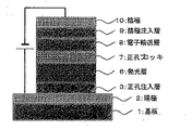
以下に図面により、本発明の電界発光素子の具体的態様の一例を説明する。
図1は、基板上に、陽極、正孔注入層、発光層、電子輸送層、陰極注入層及び陰極をこの順に形成した構造である。
ここでは陽極から正孔の注入効率を上げるために正孔注入層、一方陰極から電子の注入効率を上げるために電子注入層を挿入してある。この場合の発光機構は、陽極から正孔を注入し、陰極から電子を注入させ、それぞれが高分子化合物中をホッピング伝導し、電子は、電子輸送層を介して発光層中に入り、高分子化合物中に形成されるエキシトン(電子と正孔のペア)から半導体超微粒子へのエネルギー移動を介して、あるいは半導体超微粒子へのチャージトラッピングにより、半導体超微粒子からの発光を得る、あるいは、高分子化合物中を電子、正孔が伝導し、半導体超微粒子内に捕獲され、再結合する過程が考えられる。
An example of a specific embodiment of the electroluminescent device of the present invention will be described below with reference to the drawings.
FIG. 1 shows a structure in which an anode, a hole injection layer, a light emitting layer, an electron transport layer, a cathode injection layer, and a cathode are formed in this order on a substrate.
Here, a hole injection layer is inserted to increase the efficiency of hole injection from the anode, and an electron injection layer is inserted to increase the efficiency of electron injection from the cathode. In this case, the light emission mechanism is such that holes are injected from the anode, electrons are injected from the cathode, each conducts hopping conduction in the polymer compound, and electrons enter the light emitting layer via the electron transport layer, and the polymer Obtain luminescence from semiconductor ultrafine particles through energy transfer from exciton (electron-hole pair) formed in the compound to semiconductor ultrafine particles, or by charge trapping to semiconductor ultrafine particles, or polymer A process is considered in which electrons and holes are conducted in the compound, captured in the semiconductor ultrafine particles, and recombined.
図2は、上述した図1の構造において、更に、発光層と電子輸送層との間に、正孔ブロッキング層を形成した構造である。
図3は、基板上に、陽極、正孔注入層、正孔輸送層、発光層、電子注入層及び陰極を形成した構造である。
図4は、上述した図3の構造において、更に発光層と正孔輸送層との間に、電子ブロッキング層を形成した構造である。
FIG. 2 shows a structure in which a hole blocking layer is further formed between the light emitting layer and the electron transport layer in the structure of FIG. 1 described above.
FIG. 3 shows a structure in which an anode, a hole injection layer, a hole transport layer, a light emitting layer, an electron injection layer, and a cathode are formed on a substrate.
FIG. 4 shows a structure in which an electron blocking layer is further formed between the light emitting layer and the hole transport layer in the structure of FIG. 3 described above.
図5は、基板上に、陽極、正孔注入層、正孔輸送層、発光層、電子輸送層、電子注入層、及び陰極を形成した構造である。この構造においては、電子および正孔の輸送を、それ
ぞれ電子輸送層と正孔輸送層を設けることによって担わせ、電子および正孔の電極からの注入、輸送特性を向上させ、発光層内で効率的に再結合させることができる。
FIG. 5 shows a structure in which an anode, a hole injection layer, a hole transport layer, a light emitting layer, an electron transport layer, an electron injection layer, and a cathode are formed on a substrate. In this structure, the transport of electrons and holes is performed by providing an electron transport layer and a hole transport layer, respectively, to improve the injection and transport characteristics of the electrons and holes from the electrodes, and to improve the efficiency in the light emitting layer. Can be recombined.
以下に各層につき説明する。
<基板>
基板として用いられる材料は、固体基板であれば特に限定されるものではないが、石英やガラス板、Al、 Au等の金属板、ポリエチレンテレフタレート、ポリメタクリレート、
ポリカーボネート、ポリスルホン等の合成樹脂基板等が用いられる。
Hereinafter, each layer will be described.
<Substrate>
The material used as the substrate is not particularly limited as long as it is a solid substrate, but a quartz or glass plate, a metal plate such as Al or Au, polyethylene terephthalate, polymethacrylate,
A synthetic resin substrate such as polycarbonate and polysulfone is used.
<発光層>
発光層に用いる半導体超微粒子は、発光性物質であれば特に限定されるものではないが、、炭素(C)、ケイ素(Si)、ゲルマニウム(Ge)、錫等の周期表第IV族元素の単体、リン(黒リン)等の周期表第V族元素の単体、セレン、テルル等の周期表第VI族元素
の単体、酸化錫(IV)窒化ホウ素(BN)、リン化ホウ素(BP)、砒化ホウ素(BAs)、窒化アルミニウム(AlN)、リン化アルミニウム(AlP)、砒化アルミニウム(AlAs)、アンチモン化アルミニウム(AlSb)、窒化ガリウム(GaN)、リン化ガリウム(GaP)、砒化ガリウム(GaAs)、アンチモン化ガリウム(GaSb)、窒化インジウム(InN)、リン化インジウム(InP)、砒化インジウム(InAs)、アンチモン化インジウム(InSb)等の周期表第III族元素と周期表第V族元素との化合物、硫化アルミニウム(Al2S3)、セレン化アルミニウム(Al2Se3)、
硫化ガリウム(Ga2S3)、セレン化ガリウム(GaSe、Ga2Se3)、テルル化ガリウム(GaTe、Ga2Te3)、酸化インジウム(In2O3)、硫化インジウム(In2
S3、InS)、セレン化インジウム(In2Se3)、テルル化インジウム(In2Te3
)等の周期表第III族元素と周期表第VI族元素との化合物、酸化亜鉛(ZnO)、硫化亜
鉛(ZnS)、セレン化亜鉛(ZnSe)、テルル化亜鉛(ZnTe)、酸化カドミウム(CdO)、硫化カドミウム(CdS)、セレン化カドミウム(CdSe)、テルル化カドミウム(CdTe)、硫化水銀(HgS)、セレン化水銀(HgSe)、テルル化水銀(HgTe)等の周期表第II族元素と周期表第VI族元素との化合物、酸化銅(I)(Cu2O)等の周期表第I族元素と周期表第VI族元素との化合物、塩化銅(I)(CuCl)、臭化銅(I)(CuBr)、ヨウ化銅(I)(CuI)、塩化銀(AgCl)、臭化銀(AgBr)等の周期表第I族元素と周期表第VII族元素との化合物などが挙げられ、必要によりこれらの2種以上を併用しても良い。これらの半導体には、構成元素以外の元素が含有されていても構わない。例えばIII-V族を例にとれば、InGaP、InGaNの様な合金系であ
ってもよい。また上記材料中に、希土類元素あるいは遷移金属元素がドープされた超微粒子も使われる。例えば、ZnS:Mn、ZnS:Tb、ZnS:Ce、LaPO4:Ceなどが挙げられる。 この中
でもケイ素(Si)、ゲルマニウム(Ge)、窒化ガリウム(GaN)、リン化ガリウム(GaP)、砒化ガリウム(GaAs)、窒化インジウム(InN)、リン化インジウム(InP)、砒化インジウム(InAs)、セレン化ガリウム(GaSe、Ga2Se3)、硫化インジウム(In2S3、InS)、酸化亜鉛(ZnO)、硫化亜鉛(ZnS)、セレン化亜鉛(ZnSe)、テルル化亜鉛(ZnTe)、酸化カドミウム(CdO)、硫化カドミウム(CdS)、セレン化カドミウム(CdSe)、テルル化カドミウム(CdTe)、InGaP、InGaNなどの合金系が好ましく用いられる。
<Light-emitting layer>
The semiconductor ultrafine particles used for the light-emitting layer are not particularly limited as long as they are light-emitting substances, but may be carbon (C), silicon (Si), germanium (Ge), tin, or other group IV elements of the periodic table. Simple substance, simple substance of group V element of the periodic table such as phosphorus (black phosphorus), simple element of group VI element of the periodic table such as selenium, tellurium, tin (IV) boron nitride (BN), boron phosphide (BP), Boron arsenide (BAs), aluminum nitride (AlN), aluminum phosphide (AlP), aluminum arsenide (AlAs), aluminum antimonide (AlSb), gallium nitride (GaN), gallium phosphide (GaP), gallium arsenide (GaAs) , Gallium antimonide (GaSb), indium nitride (InN), indium phosphide (InP), indium arsenide (InAs), indium antimonide (InS) b) a compound of a group III element of the periodic table and a group V element of the periodic table, such as aluminum sulfide (Al 2 S 3 ), aluminum selenide (Al 2 Se 3 ),
Gallium sulfide (Ga 2 S 3 ), gallium selenide (GaSe, Ga 2 Se 3 ), gallium telluride (GaTe, Ga 2 Te 3 ), indium oxide (In 2 O 3 ), indium sulfide (In 2
S 3 , InS), indium selenide (In 2 Se 3 ), indium telluride (In 2 Te 3)
) And other compounds of the Periodic Table Group III and the Periodic Table Group VI, such as zinc oxide (ZnO), zinc sulfide (ZnS), zinc selenide (ZnSe), zinc telluride (ZnTe), and cadmium oxide (CdO). ), Cadmium sulfide (CdS), cadmium selenide (CdSe), cadmium telluride (CdTe), mercury sulfide (HgS), mercury selenide (HgSe), mercury telluride (HgTe), and the like. Compound with periodic table group VI element, compound of periodic table group I element with periodic table group VI element such as copper (I) oxide (Cu 2 O), copper (I) chloride (CuCl), bromide Compounds of Group I and Group VII elements of the periodic table, such as copper (I) (CuBr), copper (I) iodide (CuI), silver chloride (AgCl), and silver bromide (AgBr). If necessary, two or more of these may be used in combination. good. These semiconductors may contain elements other than the constituent elements. For example, taking the III-V group as an example, alloys such as InGaP and InGaN may be used. Ultrafine particles doped with a rare earth element or a transition metal element in the above materials are also used. For example, ZnS: Mn, ZnS: Tb, ZnS: Ce, LaPO4: Ce and the like can be mentioned. Among them, silicon (Si), germanium (Ge), gallium nitride (GaN), gallium phosphide (GaP), gallium arsenide (GaAs), indium nitride (InN), indium phosphide (InP), indium arsenide (InAs), Gallium selenide (GaSe, Ga 2 Se 3 ), indium sulfide (In 2 S 3 , InS), zinc oxide (ZnO), zinc sulfide (ZnS), zinc selenide (ZnSe), zinc telluride (ZnTe), oxide Alloys such as cadmium (CdO), cadmium sulfide (CdS), cadmium selenide (CdSe), cadmium telluride (CdTe), InGaP, and InGaN are preferably used.
また該超微粒子は、コアシェル構造を有するものであってもよい。この場合、シェル部分はコア部分を形成する半導体のバンドギャップより大きい材料である必要がある。このような例としては、CdSeコア/ZnSシェル、CdSeコア/CdSシェル、InPコア/ZnSシェル等が挙げられる。
また半導体超微粒子は、その表面、あるいは超微粒子がコアシェル構造の場合はシェル部分の表面に、有機化合物が、配位、吸着、結合等により存在していても構わない。有機化合物の存在により溶媒への溶解性が向上する。このような有機化合物としては、例えば
、トリオクチルホスフィンオキシド、トリオクチルホスフィン等のホスフィン系化合物、ヘキサデシルアミン等のアミン系化合物などが例示される。
The ultrafine particles may have a core-shell structure. In this case, the shell portion needs to be made of a material larger than the band gap of the semiconductor forming the core portion. Such examples include a CdSe core / ZnS shell, a CdSe core / CdS shell, and an InP core / ZnS shell.
In addition, the semiconductor ultrafine particles may have an organic compound present on the surface thereof, or when the ultrafine particles have a core-shell structure, by coordination, adsorption, bonding, or the like. The solubility in a solvent is improved by the presence of the organic compound. Examples of such organic compounds include phosphine compounds such as trioctylphosphine oxide and trioctylphosphine, and amine compounds such as hexadecylamine.
半導体超微粒子の平均直径の下限値は、通常、0.5nm以上、好ましくは1nm以上であり
、上限値は通常100nm以下、好ましくは10nm以下である。
発光層に用いられる高分子化合物とは、重量平均分子量が通常、2,000〜 500,000のものである。
その種類は特に限定されるものではないが、ポリパラフェニレン系高分子、ポリパラフェニレンビニレン系高分子、ポリチオフェン系高分子、ポリアニリン系高分子、ポリピロール系高分子、ポリカルバゾール系高分子、ポリビニルカルバゾール系高分子、ポリピリジン系高分子、ポリフルオレン系高分子、ポリスピロ系高分子、ポリアセチレン系高分子、ポリチエニレンビニレン系高分子、ポリフェニレンチエニレン系高分子、ポリキノン系高分子、ポリピリジン系高分子またはそれらを含む共重合体などが例示される。ただし該高分子のエネルギーギャップが、分散させる半導体超微粒子のそれよりも大きい必要がある。
The lower limit of the average diameter of the semiconductor ultrafine particles is usually 0.5 nm or more, preferably 1 nm or more, and the upper limit is usually 100 nm or less, preferably 10 nm or less.
The polymer compound used for the light emitting layer has a weight average molecular weight of usually 2,000 to 500,000.
The type is not particularly limited, but polyparaphenylene polymer, polyparaphenylene vinylene polymer, polythiophene polymer, polyaniline polymer, polypyrrole polymer, polycarbazole polymer, polyvinylcarbazole -Based polymer, polypyridine-based polymer, polyfluorene-based polymer, polyspiro-based polymer, polyacetylene-based polymer, polythienylenevinylene-based polymer, polyphenylene-enylene-based polymer, polyquinone-based polymer, polypyridine-based polymer or Copolymers containing them are exemplified. However, the energy gap of the polymer needs to be larger than that of the semiconductor ultrafine particles to be dispersed.
この中で好ましいのは、ポリパラフェニレン系高分子、ポリパラフェニレンビニレン系高分子、ポリチオフェン系高分子、ポリカルバゾール系高分子、ポリビニルカルバゾール系高分子、ポリフルオレン系高分子、ポリスピロ系高分子、ポリチエニレンビニレン系高分子、ポリフェニレンチエニレン系高分子、ポリキノン系高分子、ポリピリジン系高分子である。
また半導体超微粒子の高分子ホスト中の含有量は、発光層全量に対し、下限値が通常0.1重量%以上、好ましくは1重量%以上であり、上限値は通常30重量%以下、好ましくは20重量%以下である。
Among them, preferred are polyparaphenylene polymer, polyparaphenylenevinylene polymer, polythiophene polymer, polycarbazole polymer, polyvinylcarbazole polymer, polyfluorene polymer, polyspiro polymer, It is a polythienylenevinylene-based polymer, a polyphenylene-enylene-based polymer, a polyquinone-based polymer, or a polypyridine-based polymer.
The content of the semiconductor ultrafine particles in the polymer host has a lower limit of usually 0.1% by weight or more, preferably 1% by weight or more, and an upper limit of usually 30% by weight or less, based on the total amount of the light emitting layer. Is not more than 20% by weight.
また、発光層は主として前記した高分子化合物と半導体超微粒子で構成されるが、導電性を上げるために後述する電子輸送性化合物を少量添加するのが好ましい。
該発光層の膜厚は、特に限定されないが、通常5〜300nmの範囲が好ましく、より好ましくは20〜200nmの範囲である。
The light-emitting layer is mainly composed of the above-mentioned polymer compound and semiconductor ultrafine particles, but it is preferable to add a small amount of an electron-transporting compound described later in order to increase conductivity.
The thickness of the light emitting layer is not particularly limited, but is usually preferably in the range of 5 to 300 nm, and more preferably in the range of 20 to 200 nm.
該発光層は、塗布法、ディップコーティング法、LB法、スピンコート法、インクジェット法、ゾルゲル法、印刷法、熱昇華型印刷法などによって作製される。
<電子輸送層>
電子輸送層は、電子輸送性化合物単独で形成されてもよいし、必要により、電子輸送性化合物が高分子化合物に分散されたものであってもよい。
The light emitting layer is formed by a coating method, a dip coating method, an LB method, a spin coating method, an ink jet method, a sol-gel method, a printing method, a thermal sublimation printing method, or the like.
<Electron transport layer>
The electron transporting layer may be formed of an electron transporting compound alone, or, if necessary, an electron transporting compound dispersed in a polymer compound.
本発明に用いられる電子輸送性化合物の種類は特に限定されるものではないが、2−(4‘−tert−ブチルフェニル)−5−(4“−ビフェニル)−1,3,4−オキサジアゾールなどのオキサジアゾール化合物、3,5,3’、5‘−テトラキス−tert−ブチルジフェノキノン等のジフェノキノン化合物、 トリス(8−ヒドロキシ−キノリノ)アルミニウム(III)、ビス(8−ヒドリキソ−キノリノ)ベリリウムなどのキノリン酸錯体系化
合物、亜鉛−ビス−ベンゾキサゾール等のベンゾキサゾール化合物、亜鉛−ビス−ベンゾチアゾール等のベンゾチアゾール化合物、ルブレンなどのナフタセン系化合物、キナクドリン系化合物、ペリレン等の縮合多環芳香族系化合物、トリス(1,3−ジフェニル−1,3−プロパンジオノ)(モノフェナントロリン)ユーロピウム(III)、1−フェニル−
2−ビフェニル−5−パラ−tert−ブチルフェニル−1,3,4−トリアゾール等のトリアゾール系化合物、2,9―ジメチル−4,7−ジフェニル−1,10−フェナントロリン等のフェナントロリン系化合物などが例示され、上記化合物の中から2種以上を併用しても良い。あるいは、電子輸送性の微粒子、例えば金、銀、クロム等の金属微粒子、フラーレン、カーボンナノチューブ等を用いることもできる。これらの電子輸送性化合物を高
分子化合物中に分散させる場合の高分子化合物としては、ポリメチルメタクリレートなどが挙げられる。
Although the kind of the electron transporting compound used in the present invention is not particularly limited, 2- (4′-tert-butylphenyl) -5- (4 ″ -biphenyl) -1,3,4-oxadi Oxadiazole compounds such as azoles, diphenoquinone compounds such as 3,5,3 ', 5'-tetrakis-tert-butyldiphenoquinone, tris (8-hydroxy-quinolino) aluminum (III), bis (8-hydroxo- Quinolinic acid complex compounds such as quinolino) beryllium, benzoxazole compounds such as zinc-bis-benzoxazole, benzothiazole compounds such as zinc-bis-benzothiazole, naphthacene compounds such as rubrene, quinacdrine compounds, perylene and the like A polycondensed aromatic compound, tris (1,3-diphenyl-1,3-propanediono) (monophenanthane) Phosphorus) europium (III), 1-phenyl -
Triazole compounds such as 2-biphenyl-5-para-tert-butylphenyl-1,3,4-triazole, and phenanthroline compounds such as 2,9-dimethyl-4,7-diphenyl-1,10-phenanthroline. For example, two or more of the above compounds may be used in combination. Alternatively, electron transporting fine particles, for example, fine metal particles such as gold, silver, and chromium, fullerene, and carbon nanotubes can also be used. When the electron transporting compound is dispersed in the polymer compound, examples of the polymer compound include polymethyl methacrylate.
上記化合物によって形成される電子輸送層の膜厚は、通常5〜200nmが好ましく、より好ましくは20〜100nmである。
該電子輸送層は、塗布法、ディップコーティング法、LB法、スピンコート法、インクジェット法、ゾルゲル法、印刷法、熱昇華型印刷法あるいは真空蒸着法によって前記発光層の上に積層することにより形成する。特に塗布法、スピンコート法などの場合は、発光層を溶解させないような溶媒の選択が必要である。
The thickness of the electron transport layer formed by the above compound is generally preferably from 5 to 200 nm, more preferably from 20 to 100 nm.
The electron transport layer is formed by laminating on the light emitting layer by a coating method, a dip coating method, an LB method, a spin coating method, an inkjet method, a sol-gel method, a printing method, a thermal sublimation printing method or a vacuum evaporation method. I do. In particular, in the case of a coating method, a spin coating method, or the like, it is necessary to select a solvent that does not dissolve the light emitting layer.
<正孔輸送層>
正孔輸送層は、正孔輸送性化合物単独で形成されてもよいし、必要により、正孔輸送性化合物が高分子化合物に分散されたものであってもよい。
本発明に用いられる正孔輸送性化合物の種類は特に限定されるものではないが、N、N‘−ジフェニル−N、N’−ビス(3−メチルフェニル)1,1'−ビフェニルー4,4
‘−ジアミン、トリフェニルアミン等の芳香族第3級アミン系化合物、銅フタロシアニン等のフタロシアニン系化合物、芳香族シラン系化合物、芳香族シラザン系化合物、芳香族ホスフィン系化合物などが例示され、また高分子系では、ポリパラフェニレン系高分子、ポリパラフェニレンビニレン系高分子、ポリチオフェン系高分子、ポリアニリン系高分子、ポリピロール系高分子、ポリカルバゾール系高分子、ポリビニルカルバゾール系高分子、ポリピリジン系高分子、ポリフルオレン系高分子、ポリスピロ系高分子、ポリアセチレン系高分子、ポリチエニンレンビニレン系高分子、ポリフェニレンチエニレン系高分子またはそれらを含む共重合体などが例示される。また上記の正孔輸送性化合物からなる微粒子を用いることもできる。これらの正孔輸送性化合物は2種以上を併用してもよい。
<Hole transport layer>
The hole transporting layer may be formed of a hole transporting compound alone or, if necessary, a layer in which the hole transporting compound is dispersed in a polymer compound.
The type of the hole transporting compound used in the present invention is not particularly limited, but N, N′-diphenyl-N, N′-bis (3-methylphenyl) 1,1′-biphenyl-4,4
Aromatic tertiary amine compounds such as' -diamine and triphenylamine, phthalocyanine compounds such as copper phthalocyanine, aromatic silane compounds, aromatic silazane compounds, aromatic phosphine compounds, and the like. For molecular systems, polyparaphenylene polymers, polyparaphenylene vinylene polymers, polythiophene polymers, polyaniline polymers, polypyrrole polymers, polycarbazole polymers, polyvinylcarbazole polymers, polypyridine polymers And polyfluorene-based polymers, polyspiro-based polymers, polyacetylene-based polymers, polythienylene-lenene-based polymers, polyphenylene-enylene-based polymers, and copolymers containing them. Further, fine particles comprising the above-described hole transporting compound can also be used. These hole transporting compounds may be used in combination of two or more.
これらの正孔輸送性化合物が高分子化合物に分散される場合の高分子化合物としては、ポリメチルメタクリレートなどが挙げられる。
上記化合物によって形成される正孔輸送層の膜厚は、通常5〜200nmが好ましく、より好ましくは20〜100nmである。
該正孔輸送層は、塗布法、ディップコーティング法、LB法、スピンコート法、インクジェット法、ゾルゲル法、印刷法、熱昇華型印刷法あるいは真空蒸着法によって陽極あるいは正孔注入層(後述)の上に積層することにより形成する。特に塗布法、スピンコート法などの場合は、発光層を溶解させないような溶媒の選択が必要である。
When these hole transporting compounds are dispersed in a polymer compound, examples of the polymer compound include polymethyl methacrylate.
The thickness of the hole transport layer formed by the above compound is usually preferably from 5 to 200 nm, more preferably from 20 to 100 nm.
The hole transport layer is formed by coating, dip coating, LB, spin coating, ink jet, sol-gel, printing, thermal sublimation printing, or vacuum evaporation to form an anode or a hole injection layer (described later). It is formed by stacking on top. In particular, in the case of a coating method, a spin coating method, or the like, it is necessary to select a solvent that does not dissolve the light emitting layer.
<電子ブロッキング層>
電子ブロッキング層は、電子ブロッキング性化合物単独で形成されてもよいし、必要により、正孔輸送性化合物が高分子化合物に分散されたものであってもよい。
本発明に用いられる電子ブロッキング性を有する化合物は、正孔輸送性を有するもので、発光層の電子親和力よりも小さいものが選択される。ただし該電子ブロッキング層で用いられる材料と正孔輸送層で用いられる材料とは異なるものである必要がある。
<Electron blocking layer>
The electron blocking layer may be formed of an electron blocking compound alone or, if necessary, a hole transporting compound dispersed in a polymer compound.
As the compound having an electron blocking property used in the present invention, a compound having a hole transporting property and smaller than the electron affinity of the light emitting layer is selected. However, the material used for the electron blocking layer and the material used for the hole transport layer need to be different.
電子ブロッキング性化合物としては、例えば、N、N‘−ジフェニル−N、N’−ビス(3−メチルフェニル)1,1'−ビフェニルー4,4‘−ジアミン、トリフェニルアミ
ン等の芳香族第3級アミン系化合物、銅フタロシアニン等のフタロシアニン系化合物、芳香族シラン系化合物、芳香族シラザン系化合物、芳香族ホスフィン系化合物などが例示され、また高分子系では、ポリパラフェニレン系高分子、ポリパラフェニレンビニレン系高分子、ポリチオフェン系高分子、ポリアニリン系高分子、ポリピロール系高分子、ポリカルバゾール系高分子、ポリビニルカルバゾール系高分子、ポリピリジン系高分子、ポリフルオレン系高分子、ポリスピロ系高分子、ポリアセチレン系高分子、ポリチエニレンビニレン系高分子、ポリフェニレンチエニレン系高分子またはそれらを含む共重合体などが例
示され、2種以上を併用しても良い。また上記化合物をポリメチルメタクリレートなどの高分子化合物に分散した系でもよい。
Examples of the electron blocking compound include aromatic tertiary compounds such as N, N′-diphenyl-N, N′-bis (3-methylphenyl) 1,1′-biphenyl-4,4′-diamine and triphenylamine. Secondary amine compounds, phthalocyanine compounds such as copper phthalocyanine, aromatic silane compounds, aromatic silazane compounds, aromatic phosphine compounds, and the like. Examples of the polymer system include polyparaphenylene polymers and polyparaphenylene compounds. Phenylene vinylene polymer, polythiophene polymer, polyaniline polymer, polypyrrole polymer, polycarbazole polymer, polyvinylcarbazole polymer, polypyridine polymer, polyfluorene polymer, polyspiro polymer, polyacetylene Polymer, polythienylene vinylene polymer, polyphenyleneene Examples include a len-based polymer or a copolymer containing the same, and two or more kinds may be used in combination. Further, a system in which the above compound is dispersed in a polymer compound such as polymethyl methacrylate may be used.
上記化合物によって形成される電子ブロッキング層の膜厚は、通常1〜100nmが好ましく、より好ましくは5〜50nmである。
該電子ブロッキング層は、塗布法、ディップコーティング法、LB法、スピンコート法、インクジェット法、ゾルゲル法、印刷法、熱昇華型印刷法あるいは真空蒸着法によって前記正孔輸送層の上に積層することにより形成する。特に塗布法、スピンコート法などの場合は、発光層を溶解させないような溶媒の選択が必要である。
The thickness of the electron blocking layer formed by the above compound is usually preferably from 1 to 100 nm, more preferably from 5 to 50 nm.
The electron blocking layer is laminated on the hole transport layer by a coating method, a dip coating method, an LB method, a spin coating method, an inkjet method, a sol-gel method, a printing method, a thermal sublimation printing method or a vacuum evaporation method. Formed by In particular, in the case of a coating method, a spin coating method, or the like, it is necessary to select a solvent that does not dissolve the light emitting layer.
<正孔ブロッキング層>
正孔ブロッキング層は、正孔ブロッキング化合物単独で形成されてもよいし、必要により、正孔輸送性化合物が高分子化合物に分散されたものであってもよい。
本発明に用いられる正孔ブロッキング性を有する化合物は、電子輸送性を有するもので、かつ発光層のイオン化ポテンシャルよりも大きなものが選択される。
ただし該正孔ブロッキング層で用いられる材料と電子輸送層で用いられる材料は異なるものである必要がある。
<Hole blocking layer>
The hole blocking layer may be formed of a hole blocking compound alone, or, if necessary, a layer in which a hole transporting compound is dispersed in a polymer compound.
As the compound having a hole blocking property used in the present invention, a compound having an electron transporting property and having a higher ionization potential than the light emitting layer is selected.
However, the material used for the hole blocking layer and the material used for the electron transport layer need to be different.
正孔ブロッキング性化合物としては、例えば、2−(4‘−tert−ブチルフェニル)−5−(4“−ビフェニル)−1,3,4−オキサジアゾールなどのオキサジアゾール化合物、3,5,3’、5‘−テトラキス−tert−ブチルジフェノキノン等のジフェノキノン化合物、トリス(8−ヒドロキシ−キノリノ)アルミニウム(III)、ビス(8−ヒドリキ
ソ−キノリノ)ベリリウムなどのキノリン酸錯体系化合物、亜鉛―ビス−ベンゾキサゾール等のベンゾキサゾール化合物、亜鉛-ビス−ベンゾチアゾール等のベンゾチアゾール化
合物、トリス(1,3−ジフェニル−1,3−プロパンジオノ)(モノフェナントロリン)ユーロピウム(III)、1−フェニル−2−ビフェニル−5−パラ−tert−ブチルフェニ
ル−1,3,4−トリアゾール等のトリアゾール系化合物、2,9―ジメチル−4,7
−ジフェニル−1,10−フェナントロリン等のフェナントロリン系化合物、ポリキノン系高分子、ポリピリジン系高分子などが例示され、また金、銀、クロム等の金属微粒子、フラーレン、カーボンナノチューブ等も用いることができる。
これらは2種以上を併用してもよい。また上記化合物をポリメチルメタクリレートなどの高分子に分散した系でもよい。
上記化合物によって形成される正孔ブロッキング層の膜厚は、通常1〜100nmが好ましく、より好ましくは5〜50nmである。
Examples of the hole blocking compound include oxadiazole compounds such as 2- (4′-tert-butylphenyl) -5- (4 ″ -biphenyl) -1,3,4-oxadiazole; Diphenoquinone compounds such as 3,3 ', 5'-tetrakis-tert-butyldiphenoquinone, quinolinic acid complex compounds such as tris (8-hydroxy-quinolino) aluminum (III) and bis (8-hydroxo-quinolino) beryllium; Benzoxazole compounds such as zinc-bis-benzoxazole, benzothiazole compounds such as zinc-bis-benzothiazole, tris (1,3-diphenyl-1,3-propanediono) (monophenanthroline) europium (III), Triazols such as 1-phenyl-2-biphenyl-5-para-tert-butylphenyl-1,3,4-triazole System compounds, 2,9-dimethyl-4,7
Examples thereof include phenanthroline-based compounds such as -diphenyl-1,10-phenanthroline, polyquinone-based polymers, and polypyridine-based polymers, and fine metal particles such as gold, silver, and chromium, fullerene, and carbon nanotubes can also be used.
These may be used in combination of two or more. Further, a system in which the above compound is dispersed in a polymer such as polymethyl methacrylate may be used.
The thickness of the hole blocking layer formed by the above compound is generally preferably from 1 to 100 nm, more preferably from 5 to 50 nm.
正孔ブロッキング層は、塗布法、ディップコーティング法、LB法、スピンコート法、インクジェット法、ゾルゲル法、印刷法、熱昇華型印刷法あるいは真空蒸着法によって前記発光層の上に積層することにより形成する。特に塗布法、スピンコート法などの場合は、発光層を溶解させないような溶媒の選択が必要である。 The hole blocking layer is formed by laminating on the light emitting layer by a coating method, a dip coating method, an LB method, a spin coating method, an inkjet method, a sol-gel method, a printing method, a thermal sublimation printing method or a vacuum evaporation method. I do. In particular, in the case of a coating method, a spin coating method, or the like, it is necessary to select a solvent that does not dissolve the light emitting layer.
<陰極及び電子注入層>
本発明の陰極材料は、発光層または電子輸送層に電子を注入する役割を果たすものである。陰極として用いられる材料は、導電性のものであれば特に制限はなく使用されるが、効率よく電子注入を行うには、仕事関数の低い金属が好ましく、スズ、マグネシウム、インジウム、カルシウム、アルミニウム、銀等の適当な金属またはそれらの合金が用いられる。例えば、マグネシウム−銀合金、マグネシウム−インジウム合金、アルミニウム−リチウム合金等が例示される。更に、陰極と他の層との界面に薄い電子注入層を導入することで、陰極からの電子注入効率を増加させることが可能である。該注入層に用いられる材料として、LiF、MgF2、Li2O、MgO、Al2O3などが例示される。該電子注入層の膜厚は、通常0.1〜5nm、このましくは0.5nm〜2nm程度である。
<Cathode and electron injection layer>
The cathode material of the present invention plays a role of injecting electrons into the light emitting layer or the electron transport layer. The material used as the cathode is not particularly limited as long as it is conductive, but for efficient electron injection, a metal having a low work function is preferable, and tin, magnesium, indium, calcium, aluminum, A suitable metal such as silver or an alloy thereof is used. For example, a magnesium-silver alloy, a magnesium-indium alloy, an aluminum-lithium alloy and the like are exemplified. Further, by introducing a thin electron injection layer at the interface between the cathode and another layer, it is possible to increase the efficiency of electron injection from the cathode. Examples of the material used for the injection layer include LiF, MgF 2 , Li 2 O, MgO, and Al 2 O 3 . The thickness of the electron injection layer is usually 0.1 to 5 nm, preferably about 0.5 to 2 nm.
<陽極及び正孔注入層>
本発明に用いられる陽極材料としては、導電性のものであれば特に制限はないが、金属、金属酸化物、高分子化合物等が挙げられる。具体的には、ドープにより導電性を付与したSi、インジウム錫酸化物(ITO)、Au,Ag、Al、ポリアニリン等が挙げられる。また固体基板上に前記導電性材料を蒸着法、CVD法、スパッタ法、電子線蒸着法、イオンビーム蒸着法、分子線エピタキシー法、塗布法、ディップコーティング法、ラングミュア−ブロジェット(LB)法、自己集積(セルフアセンブリ)法、スピンコート法、インクジェット法、ゾルゲル法により積層させたものを用いても構わない。
<Anode and hole injection layer>
The anode material used in the present invention is not particularly limited as long as it is conductive, and examples thereof include metals, metal oxides, and high molecular compounds. Specific examples include Si, indium tin oxide (ITO), Au, Ag, Al, and polyaniline, which have been given conductivity by doping. The conductive material is deposited on a solid substrate by vapor deposition, CVD, sputtering, electron beam vapor deposition, ion beam vapor deposition, molecular beam epitaxy, coating, dip coating, Langmuir-Blodget (LB), Those laminated by a self-integration (self-assembly) method, a spin coating method, an inkjet method, or a sol-gel method may be used.
また陽極から正孔を注入する際の障壁を低くさせるために、陽極と他の層との界面に正孔注入層を導入してもよい。この場合、陽極の仕事関数と発光層のイオン化ポテンシャルの中間に位置するものを選択する。例えば、ポリエチレンジオキシチオフェン/ポリスチレンサルフォネート(PEDOT/PSS)、ポリアニリン、スターバーストアミン化合物、銅フ
タロシアニン、アモルファスカーボン、MoOx、SiO2などが例示される。
Further, a hole injection layer may be introduced at an interface between the anode and another layer in order to lower a barrier when holes are injected from the anode. In this case, a material located between the work function of the anode and the ionization potential of the light emitting layer is selected. For example, polyethylene dioxythiophene / polystyrene sulfonate (PEDOT / PSS), polyaniline, starburst amine compound, copper phthalocyanine, amorphous carbon, MoOx, SiO 2 and the like are exemplified.
上記化合物によって形成される正孔注入層の膜厚は、通常5〜1000nm、好ましくは10〜500nmである。 The thickness of the hole injection layer formed by the above compound is usually 5 to 1000 nm, preferably 10 to 500 nm.
以下に、実施例により本発明の具体的態様を更に詳細に説明するが、本発明はその要旨を超えない限り、これらの実施例によって限定されるものではない。
実施例1
ITO基板を、アセトンで超音波洗浄、乾燥窒素で乾燥後、使用した。半導体超微粒子は、ホットソープ法(J. Am. Chem. Soc. 115(1993) 8706, 特表2001-523758
号公報)によりCdSeコア/ZnSシェル(CdSe/ZnS)を合成した。
この方法で作製される超微粒子の表面に、トリオクチルフォスフィンオキシドが配位しており、有機溶媒に可溶である。また発光層に用いる高分子化合物としては、ポリ−N―ビニルカルバゾール(PVK)を使用した。 まずITO基板上に正孔注入層として、ポリエチレンジオキシチオフェン/ポリスチレンサルフォネート(PEDOT/PSS)水溶液を10
00rpmの条件でスピンコートにより成膜した。膜厚は30nmであった。この層の上に発光層として、クロロフォルム200mlにCdSe/ZnS 0.2mgとポリ−N―ビニル
カルバゾール 2mgを混合し、1000rpmの条件でスピンコートした。膜厚は80nmであった。
更に発光層の上に電子輸送性化合物である2−(4‘−tert−ブチルフェニル)−5−(4“−ビフェニル)−1,3,4−オキサジアゾールを真空蒸着で成膜した。この時の蒸着速度は、5nm/秒で、膜厚は30nmであった。更に該電子輸送層の上に陰極バッ
ファ層MgF2を1.5nm成膜し、その上にAlを200nm形成した。蒸着時の真空度は、1x10⁻³Torrであった。作製された素子を真空中に保持し、電界発光特性を調べた。図6に上記素子によって得られた
電界発光スペクトルを示す。バイアス電圧は24Vである。約560nmにピークを持つこのスペクトルは、CdSe/ZnSのみからの発光である。更に26Vに電圧を上げても、CdSe/ZnSからの発光強度が増加し、素子の劣化はみられなかった。
Hereinafter, specific embodiments of the present invention will be described in more detail with reference to Examples. However, the present invention is not intended to be limited to these Examples unless it exceeds the gist thereof.
Example 1
The ITO substrate was ultrasonically cleaned with acetone, dried with dry nitrogen, and then used. Semiconductor ultrafine particles can be obtained by a hot soap method (J. Am. Chem. Soc. 115 (1993) 8706, JP-T-2001-523758).
Publication), a CdSe core / ZnS shell (CdSe / ZnS) was synthesized.
Trioctylphosphine oxide is coordinated on the surface of the ultrafine particles produced by this method, and is soluble in an organic solvent. In addition, poly-N-vinylcarbazole (PVK) was used as a polymer compound used for the light emitting layer. First, an aqueous solution of polyethylene dioxythiophene / polystyrene sulfonate (PEDOT / PSS) was used as a hole injection layer on an ITO substrate.
The film was formed by spin coating under the condition of 00 rpm. The thickness was 30 nm. On this layer, as a light-emitting layer, 200 mg of chloroform was mixed with 0.2 mg of CdSe / ZnS and 2 mg of poly-N-vinylcarbazole, and spin-coated at 1000 rpm. The film thickness was 80 nm.
Further, 2- (4′-tert-butylphenyl) -5- (4 ″ -biphenyl) -1,3,4-oxadiazole as an electron transporting compound was formed on the light emitting layer by vacuum evaporation. At this time, the deposition rate was 5 nm / sec, the film thickness was 30 nm, a 1.5-nm cathode buffer layer MgF2 was formed on the electron transport layer, and 200-nm Al was formed thereon. The degree of vacuum at that time was 1 × 10 −3 Torr.The fabricated device was held in vacuum, and the electroluminescence characteristics were examined, and the electroluminescence spectrum obtained by the above device is shown in FIG. This spectrum having a peak at about 560 nm is light emission only from CdSe / ZnS.Even if the voltage is further increased to 26 V, the light emission intensity from CdSe / ZnS increases, and deterioration of the device is observed. Did not.
実施例2
発光層としてPVK中にCdSe/ZnS半導体超微粒子分散させたもので、素子の構成は実施例1と同じであるが、発光層作製のスピンコート条件を1300rpmにして、素子を作製した。この場合の発光層膜厚は約60nmであった。この素子の電界発光スペクトルをみると、PVK由来の発光とCdSe/ZnS半導体超微粒子からの発光が同時に観測され、ピーク位置はそれぞれ約420nmと約560nmであった。それぞれのピーク強度の電圧依
存性の関係を図7に示す。図から明らかなように、PVKからの発光にくらべて、CdSe/ZnS半導体超微粒子からの発光の電圧に対する発光強度の増加率が高く、高電圧(大電流)においても発光強度の低下は見られなかった。かつPVKにCdSe/ZnS半導体超微粒子が分散されていることによって、PVKからの発光の劣化の程度も比較例1の場合に比べて抑えられていることが示された。
Example 2
CdSe / ZnS semiconductor ultrafine particles were dispersed in PVK as a light emitting layer, and the structure of the device was the same as that of Example 1. However, the spin coating conditions for forming the light emitting layer were set at 1300 rpm to manufacture the device. In this case, the thickness of the light emitting layer was about 60 nm. Looking at the electroluminescence spectrum of this device, light emission derived from PVK and light emission from CdSe / ZnS semiconductor ultrafine particles were simultaneously observed, and the peak positions were about 420 nm and about 560 nm, respectively. FIG. 7 shows the voltage dependence of each peak intensity. As is apparent from the figure, the rate of increase of the light emission intensity with respect to the voltage of light emission from the CdSe / ZnS semiconductor ultrafine particles is higher than that of light emission from PVK, and the light emission intensity is reduced even at a high voltage (large current). Did not. In addition, it was shown that the degree of degradation of light emission from PVK was suppressed as compared with Comparative Example 1 by dispersing the CdSe / ZnS semiconductor ultrafine particles in PVK.
比較例1
発光層をCdSe/ZnS半導体超微粒子を用いずPVKのみとした以外、実施例1と同様の素子構成で作製した。この場合には、PVKからの発光が420nmが見られた。発光スペクトルの電圧依存性をみると、18Vでは発光強度(任意単位)が約20000であったものが、22Vでは約5000と1/4まで減少し、26Vでは約500と1/40まで減少した。実施例1のCdSe/ZnS半導体超微粒子を分散させた場合に比べて、素子の劣化が激しいことが示された。
Comparative Example 1
The light emitting layer was manufactured with the same element configuration as in Example 1 except that the light emitting layer was made of only PVK without using ultrafine CdSe / ZnS semiconductor particles. In this case, light emission from the PVK was 420 nm. Looking at the voltage dependence of the emission spectrum, the emission intensity (arbitrary unit) was about 20,000 at 18 V, but decreased to about 5000 and 1/4 at 22 V, and decreased to about 500 and 1/40 at 26 V. . As compared with the case where the ultrafine CdSe / ZnS semiconductor particles of Example 1 were dispersed, it was shown that the element was significantly deteriorated.
比較例2
実施例1において、電子輸送層を形成しない以外同様にして素子を形成し、実施例1と同様に評価した。図8に上記素子によって得られた電子発光スペクトルを示す。約440nm近傍にPVK由来のブロードな発光ピークが観測されたが、CdSe/ZnS半導体超微粒子からの発光はほとんど観測されなかった。ここでスパイク状のピークが数本観測されるが、これはノイズである。
比較例3
実施例1において、PVKの代わりにトリフェニルアミン誘導体(TPD)として、N,N′−ビス(3−メチルフェニル)−N,N′−ジフェニルベンジン(分子量516.69)を用いた以外同様に行った。マトリックスとして低分子(TPD)を用いた場合、経時的に非発光部分(ダークスポット)の発生がみられ、素子としての安定性が劣るものであった。
Comparative Example 2
A device was formed in the same manner as in Example 1 except that the electron transporting layer was not formed, and evaluated in the same manner as in Example 1. FIG. 8 shows an electroluminescence spectrum obtained by the above device. A broad emission peak derived from PVK was observed at about 440 nm, but emission from CdSe / ZnS semiconductor ultrafine particles was hardly observed. Here, several spike-shaped peaks are observed, which are noise.
Comparative Example 3
Example 1 was repeated except that N, N'-bis (3-methylphenyl) -N, N'-diphenylbenzine (molecular weight 516.69) was used as the triphenylamine derivative (TPD) in place of PVK. . When a low molecular weight (TPD) was used as the matrix, non-light-emitting portions (dark spots) were generated over time, and the stability of the device was poor.
Claims (6)
Priority Applications (1)
| Application Number | Priority Date | Filing Date | Title |
|---|---|---|---|
| JP2003367348A JP2004172102A (en) | 2002-10-29 | 2003-10-28 | Electroluminescent device |
Applications Claiming Priority (2)
| Application Number | Priority Date | Filing Date | Title |
|---|---|---|---|
| JP2002314298 | 2002-10-29 | ||
| JP2003367348A JP2004172102A (en) | 2002-10-29 | 2003-10-28 | Electroluminescent device |
Publications (1)
| Publication Number | Publication Date |
|---|---|
| JP2004172102A true JP2004172102A (en) | 2004-06-17 |
Family
ID=32715760
Family Applications (1)
| Application Number | Title | Priority Date | Filing Date |
|---|---|---|---|
| JP2003367348A Withdrawn JP2004172102A (en) | 2002-10-29 | 2003-10-28 | Electroluminescent device |
Country Status (1)
| Country | Link |
|---|---|
| JP (1) | JP2004172102A (en) |
Cited By (15)
| Publication number | Priority date | Publication date | Assignee | Title |
|---|---|---|---|---|
| WO2005020642A1 (en) * | 2003-08-20 | 2005-03-03 | Tdk Corporation | Organic el device and method for manufacturing same |
| JP2006185985A (en) * | 2004-12-27 | 2006-07-13 | Sony Corp | Light emitting device and manufacturing method thereof |
| WO2007010880A1 (en) * | 2005-07-15 | 2007-01-25 | Seiko Epson Corporation | Light emitting device and electronic equipment provided with the light emitting device |
| JP2007184516A (en) * | 2006-01-03 | 2007-07-19 | Jiaotong Univ | Method for producing nanocomposite for polymer light emitting diode |
| WO2009057317A1 (en) * | 2007-11-01 | 2009-05-07 | Panasonic Corporation | Light-emitting device and display device |
| WO2009081918A1 (en) * | 2007-12-26 | 2009-07-02 | Idemitsu Kosan Co., Ltd. | Organic/inorganic hybrid electroluminescent element |
| JP2010535262A (en) * | 2007-07-31 | 2010-11-18 | ナノコ テクノロジーズ リミテッド | Nanoparticles |
| WO2012053398A1 (en) * | 2010-10-22 | 2012-04-26 | コニカミノルタホールディングス株式会社 | Organic electroluminescent element |
| JP2012231154A (en) * | 2006-02-09 | 2012-11-22 | Qd Vision Inc | Device comprising layer including semiconductor nanocrystal and doped organic material and method of manufacturing the same |
| JP2014534581A (en) * | 2011-10-31 | 2014-12-18 | ナンヤン・テクノロジカル・ユニバーシティー | Light emitting device |
| US9096425B2 (en) | 2006-06-24 | 2015-08-04 | Qd Vision, Inc. | Methods for depositing nanomaterial, methods for fabricating a device, methods for fabricating an array of devices and compositions |
| US9120149B2 (en) | 2006-06-24 | 2015-09-01 | Qd Vision, Inc. | Methods and articles including nanomaterial |
| US9349975B2 (en) | 2006-09-12 | 2016-05-24 | Qd Vision, Inc. | Composite including nanoparticles, methods, and products including a composite |
| JP2018022862A (en) * | 2016-07-20 | 2018-02-08 | 株式会社Joled | Organic electroluminescent element, organic electroluminescent device, and electronic apparatus |
| JP2021523530A (en) * | 2018-05-11 | 2021-09-02 | ナノシス・インク. | Quantum dot LED design based on resonance energy transfer |
-
2003
- 2003-10-28 JP JP2003367348A patent/JP2004172102A/en not_active Withdrawn
Cited By (22)
| Publication number | Priority date | Publication date | Assignee | Title |
|---|---|---|---|---|
| US7897269B2 (en) | 2003-08-20 | 2011-03-01 | Tdk Corporation | Organic EL elements and process for fabrication thereof |
| WO2005020642A1 (en) * | 2003-08-20 | 2005-03-03 | Tdk Corporation | Organic el device and method for manufacturing same |
| JP2006185985A (en) * | 2004-12-27 | 2006-07-13 | Sony Corp | Light emitting device and manufacturing method thereof |
| WO2007010880A1 (en) * | 2005-07-15 | 2007-01-25 | Seiko Epson Corporation | Light emitting device and electronic equipment provided with the light emitting device |
| JP2007027355A (en) * | 2005-07-15 | 2007-02-01 | Seiko Epson Corp | Light emitting element and electronic device |
| US8212471B2 (en) | 2005-07-15 | 2012-07-03 | Seiko Epson Corporation | Light emitting device and electronic equipment provided with the light emitting device |
| JP2007184516A (en) * | 2006-01-03 | 2007-07-19 | Jiaotong Univ | Method for producing nanocomposite for polymer light emitting diode |
| JP2012231154A (en) * | 2006-02-09 | 2012-11-22 | Qd Vision Inc | Device comprising layer including semiconductor nanocrystal and doped organic material and method of manufacturing the same |
| US9120149B2 (en) | 2006-06-24 | 2015-09-01 | Qd Vision, Inc. | Methods and articles including nanomaterial |
| US9096425B2 (en) | 2006-06-24 | 2015-08-04 | Qd Vision, Inc. | Methods for depositing nanomaterial, methods for fabricating a device, methods for fabricating an array of devices and compositions |
| US9349975B2 (en) | 2006-09-12 | 2016-05-24 | Qd Vision, Inc. | Composite including nanoparticles, methods, and products including a composite |
| JP2010535262A (en) * | 2007-07-31 | 2010-11-18 | ナノコ テクノロジーズ リミテッド | Nanoparticles |
| JPWO2009057317A1 (en) * | 2007-11-01 | 2011-03-10 | パナソニック株式会社 | LIGHT EMITTING ELEMENT AND DISPLAY DEVICE |
| WO2009057317A1 (en) * | 2007-11-01 | 2009-05-07 | Panasonic Corporation | Light-emitting device and display device |
| WO2009081918A1 (en) * | 2007-12-26 | 2009-07-02 | Idemitsu Kosan Co., Ltd. | Organic/inorganic hybrid electroluminescent element |
| WO2012053398A1 (en) * | 2010-10-22 | 2012-04-26 | コニカミノルタホールディングス株式会社 | Organic electroluminescent element |
| US8759826B2 (en) | 2010-10-22 | 2014-06-24 | Konica Minolta, Inc. | Organic electroluminescent element |
| JPWO2012053398A1 (en) * | 2010-10-22 | 2014-02-24 | コニカミノルタ株式会社 | Organic electroluminescence device |
| JP2014534581A (en) * | 2011-10-31 | 2014-12-18 | ナンヤン・テクノロジカル・ユニバーシティー | Light emitting device |
| JP2018022862A (en) * | 2016-07-20 | 2018-02-08 | 株式会社Joled | Organic electroluminescent element, organic electroluminescent device, and electronic apparatus |
| JP2021523530A (en) * | 2018-05-11 | 2021-09-02 | ナノシス・インク. | Quantum dot LED design based on resonance energy transfer |
| JP2024051110A (en) * | 2018-05-11 | 2024-04-10 | 昭栄化学工業株式会社 | Illumination device and QD-LED device |
Similar Documents
| Publication | Publication Date | Title |
|---|---|---|
| CN101810055B (en) | Light emitting element | |
| Chang et al. | High-efficiency organic electroluminescent device with multiple emitting units | |
| JP3327558B2 (en) | Organic / inorganic alloys used to improve organic electroluminescent devices | |
| CN102544374B (en) | Organic semiconductor element | |
| CN100459207C (en) | organic electroluminescent element | |
| CN102176514B (en) | Intermediate electrodes for stacked oleds | |
| US6806491B2 (en) | Organic light-emitting devices | |
| US6274979B1 (en) | Organic light emitting diodes | |
| KR102191703B1 (en) | Perovskite light-emitting device having passivation layer and fabrication method therof | |
| JP2002100482A (en) | Organic electroluminescent device | |
| JP2005251587A (en) | Organic el device | |
| CN1781198A (en) | Light-emitting devices with fullerene layer | |
| JP2009088276A (en) | Light emitting element | |
| JP2004172102A (en) | Electroluminescent device | |
| JP2010103534A (en) | Organic light-emitting diode device having nano-dot and method of manufacturing same | |
| JP2004253175A (en) | Electroluminescent device | |
| JP2009087754A (en) | Light emitting element | |
| CN102017799A (en) | Electroluminescence element, display device, and lighting device | |
| US7919771B2 (en) | Composition for electron transport layer, electron transport layer manufactured thereof, and organic electroluminescent device including the electron transport layer | |
| JP2016532246A (en) | Frequency dependent light emitting device | |
| JP2009087756A (en) | Light emitting element | |
| JP2008300270A (en) | Light emitting element | |
| JP2009087755A (en) | Light emitting element | |
| Chou et al. | Hybrid white-light emitting-LED based on luminescent polyfluorene polymer and quantum dots | |
| KR100595928B1 (en) | Organic light emitting device having a light emitting layer of dotted doping structure using a mixed host material |
Legal Events
| Date | Code | Title | Description |
|---|---|---|---|
| A621 | Written request for application examination |
Free format text: JAPANESE INTERMEDIATE CODE: A621 Effective date: 20061005 |
|
| A761 | Written withdrawal of application |
Free format text: JAPANESE INTERMEDIATE CODE: A761 Effective date: 20071210 |