JP2004042493A - Mold and optical element - Google Patents
Mold and optical element Download PDFInfo
- Publication number
- JP2004042493A JP2004042493A JP2002204394A JP2002204394A JP2004042493A JP 2004042493 A JP2004042493 A JP 2004042493A JP 2002204394 A JP2002204394 A JP 2002204394A JP 2002204394 A JP2002204394 A JP 2002204394A JP 2004042493 A JP2004042493 A JP 2004042493A
- Authority
- JP
- Japan
- Prior art keywords
- molding
- mold
- molding die
- fine shape
- shape
- Prior art date
- Legal status (The legal status is an assumption and is not a legal conclusion. Google has not performed a legal analysis and makes no representation as to the accuracy of the status listed.)
- Withdrawn
Links
Images


Landscapes
- Diffracting Gratings Or Hologram Optical Elements (AREA)
- Moulds For Moulding Plastics Or The Like (AREA)
Abstract
【課題】成形品の型からの離型を高精度に行なうことができるようにする。
【解決手段】樹脂材料に所望の光学機能を有する微細形状を転写して、光学素子を成形するための成形用型6であって、微細形状を樹脂材料に転写するための第1の成形面8と、第1の成形面の有効範囲外に設けられ、微細形状の深さよりも深い凹形状部7を有する第2の成形面とを具備する。
【選択図】 図6An object of the present invention is to release a molded product from a mold with high precision.
A molding die (6) for transferring a fine shape having a desired optical function to a resin material to form an optical element, the first forming surface for transferring the fine shape to the resin material. 8 and a second molding surface provided outside the effective range of the first molding surface and having a concave portion 7 deeper than the depth of the fine shape.
[Selection] Fig. 6
Description
【0001】
【発明の属する技術分野】
本発明は、樹脂材料の表面に所望の光学機能を有する微細形状を転写するための成形用型及びその型により成形された光学素子に関するものである。
【0002】
【従来の技術】
従来、回折光学素子の成形技術のひとつとして、大面積成形性と高転写性に優れ、その成形技術の容易さから大量生産に適しているレプリカ成形技術がある。このレプリカ成形技術は、所望の光学形状の反転形状を有する型の成形面上に光硬化性樹脂を滴下し、その上からレンズブランクを圧着させて樹脂を押し広げ、所望の形状になったところで、光源からの光を照射して光硬化性樹脂を硬化させ、当該硬化樹脂をレンズブランクと共に離型することで成形を行うものである。
【0003】
このようなレプリカ成形での離型においては、硬化樹脂が型表面に密着あるいは接着してしまったり、また微細形状が離型時の応力により変形あるいは欠損するなどして、成形品を容易に精度良く離型することが困難である。
【0004】
そのため、所望形状を有する回折光学素子を成形するレプリカ成形法においては、離型性を向上させて転写性に優れた高精度な成形品を得るための離型方法が数多く提案されている。
【0005】
離型性を向上させる公知技術としては、既に一般的な手法である離型剤の型成形面への塗布、または離型剤の樹脂材料への添加などが知られている。また、より具体的な手法としては、特開平5−50442号公報において、型の光学有効径外に、疎密性物質を塗布するか又は離型時応力を最大限に有効とする所定の形状を設けることにより、型と成形品との初期密着力を低下させる方法が提案されている。また、特開平4−144718号公報においては、上下動自在な内型と外型で構成された成形型の内型と外型のどちらか一方を上下動させて外周部に亀裂を生じさせ、離型を容易にする方法が提案されている。
【0006】
【発明が解決しようとする課題】
しかしながら、上記の公報に開示されている技術は、所望の微細形状を有する回折光学素子のレプリカ離型に適応できない場合もあり、より高精度な成形性と効率的な生産性を求める場合には次に挙げるような問題が発生する。
【0007】
平面又は曲面の光学機能面上に微細形状を有する回折光学素子をレプリカ成形する場合の離型において、離型時応力による格子の変形又は欠損はある程度は避けがたいものである。レプリカ離型においては、微細形状部に複雑に分布する離型時応力が負荷され、微小な格子部等に変形や欠損を与える。これらの変形や欠損部は光学素子の光学性能を著しく低下させることは言うまでもない。
【0008】
そこで、この障害を回避するための方法の一つとして、型成形面上に離型剤を塗布して型と硬化樹脂との密着力を低下させる手法が挙げられるが、液剤塗布の表面張力による膜厚差又は液垂れなどで、極めて精密に加工された成形面上の光学微細形状が歪むことになる。
【0009】
一方、離型剤を樹脂材料そのものへ添加する手法においては、樹脂材料の耐環境性の悪化や屈折率低下等の影響が観察され、回折光学素子を成形する光学材料としては好ましくない。
【0010】
また、レプリカ離型時の初期密着力を低下させるための特開平5−50442号公報に開示される成形用型においては、離型時の初期密着力は低下させることができても光学微細形状部に負荷される離型時応力まではその効果が得られない。
【0011】
さらに、特開平4−144718号公報に開示される成形用型においても、同様に光学微細形状部に負荷される離型時応力までは低減させることができないだけでなく、型作動行程による生産タクトの長時間化、また生産装置自体の大規模化につながることから、生産性を低下させるだけでなく大幅なコストアップとなる。
【0012】
したがって、本発明は上述した課題に鑑みてなされたものであり、その目的は、成形品の型からの離型を高精度に行なえるようにすることである。
【0013】
【課題を解決するための手段】
上述した課題を解決し、目的を達成するために、本発明に係わる成形用型は、樹脂材料に所望の光学機能を有する微細形状を転写して、光学素子を成形するための成形用型であって、前記微細形状を前記樹脂材料に転写するための第1の成形面と、該第1の成形面の有効範囲外に設けられ、前記微細形状の深さよりも深い凹形状部を有する第2の成形面とを具備することを特徴としている。
【0014】
また、この発明に係わる成形用型において、前記微細形状は、前記光学機能として光回折機能を有することを特徴としている。
【0015】
また、この発明に係わる成形用型において、前記微細形状は、同心円状の凹凸から構成されていることを特徴としている。
【0016】
また、この発明に係わる成形用型において、前記凹形状部は、前記微細形状の有効径外に、前記微細形状と同心円状に形成されていることを特徴としている。
【0017】
また、この発明に係わる成形用型において、前記凹形状部は、断面形状が長方形の溝からなることを特徴としている。
【0018】
また、この発明に係わる成形用型において、前記凹形状部は、断面形状が台形の溝からなることを特徴としている。
【0019】
また、この発明に係わる成形用型において、前記凹形状部は、断面形状がV字形の溝からなることを特徴としている。
【0020】
また、本発明に係わる光学素子は、微細形状が形成された光学機能面と、該光学機能面の有効範囲外に配置され、前記微細形状よりも高さが高い凸形状部とを具備することを特徴としている。
【0021】
また、この発明に係わる光学素子において、前記微細形状は、光学機能として光回折機能を有することを特徴としている。
【0022】
【発明の実施の形態】
以下、本発明の好適な実施形態について説明する。
【0023】
まず、本実施形態の概要について説明する。
【0024】
本実施形態では、光学的所望の微細形状を有する型面上に光硬化性樹脂を滴下し、該光硬化性樹脂を、平面または曲面ガラス基板で押圧し、光照射することにより回折光学素子を成形する成形用型において、前記成形用型の光学有効部外の成形面に、所望の光学機能面における微細形状深さに比べても十分に深い溝または開口形状を設ける。
【0025】
また、所望とする回折光学素子の同心円状または縦縞状の微細形状の反転形状が型成形面に加工されており、この型面の微細形状の光硬化性樹脂による形状成形が、当該成形用型の光学有効外に設けられた所望の光学機能面における微細形状深さに比べても十分に深い溝または開口形状の光硬化性樹脂による形状成形と同時に行われるように、成形面を構成している。
【0026】
また、本実施形態の回折光学素子は、成形用型で所謂レプリカ成形により形成される成形回折光学素子であって、その光学有効部外に、所望の光学機能面における微細形状高さに比べても十分に高い凸形状が形成されている。
【0027】
上記の構成を用いることにより、以下に示すような効果を得ることができる。図1は、レプリカ成形の離型プロセスを示す模式図である。レンズブランク1と成形型2により押圧された樹脂3が硬化成形された後に、外力Fを加えて離型させるプロセスを示す。
【0028】
図2は、離型初期における成形型左端部の離型時応力状態を示している。外力Fによる左端部第1格子に負荷される離型力fの分力はそれぞれ、レンズブランク1と樹脂3の反りによる向心力f2、さらに反り曲面の接線方向における力f1に分けることができる。これらの離型時応力は、離型が進行していくと同時に各格子に連続的に負荷されるものである。
【0029】
レプリカ離型における格子の変形または欠損を発生させる応力は、図示のf1であり、本実施形態は、離型時応力f1を容易な手法で低下または分散させる構成を示す。
【0030】
図3は、本実施形態の構成によるレプリカ成形の離型プロセスを示す模式図である。
【0031】
光学有効部外の成形面に光学機能面における微細形状深さに比べても十分に深い溝または開口形状4を設けた成形型5により押圧された樹脂3が硬化成形された後の、外力Fによる離型プロセスを示す。
【0032】
図4は成形型5の離型初期における成形型左端部の離型時応力状態を示している。
【0033】
外力Fによる左端部溝形状部に負荷される離型力f3の分力はそれぞれ、レンズブランク1と樹脂3の反りによる向心力f5、さらに反り曲面の接線方向における力f4に分けることができる。さらにこのとき、光学機能面である左端第1格子部においても、格子の変形または欠損を発生させる応力f1’が多少なりとも負荷されることになる。しかし、溝形状部4への応力集中または光学機能面での応力分散により、レンズブランク1や樹脂3の離型力Fによる反りも緩和され、離型時応力f1’を変形または欠損を与えない程度の微力に十分抑えることができる。また離型時応力f1’は、離型が進行していくと同時に各格子に連続的に負荷されるが、溝形状部4の高さを光学機能面の格子高さに比べて十分に高くとることで、光学機能面の離型を溝形状部4の離型よりも先に終了させ、離型時応力を終始溝形状部4に集中させておくことができる。
【0034】
したがって、離型時応力による光学機能面格子の変形または欠損を軽減させ、微細形状を有する回折光学素子のレプリカ成形における生産性を向上し、コスト削減を図り、かつ十分な光学的機能を満たした所望形状のレプリカ成形品を得ることができる。
【0035】
(第1の実施形態)
図5は本発明の第1の実施形態に係わるレプリカ成形装置の概略構成を示す図である。
【0036】
図5において、6は所望とする光学機能形状の反転形状8と溝形状部7をその成形面に設けた成形型である。成形型6は固定されており、成形型6を嵌め込んでいるリング状のレンズブランク保持部材9上にはレンズブランク10が載置され、レンズブランク10の中心軸と成形型6の成形面の中心軸との位置合わせは、レンズブランク保持部材9の嵌合部にレンズブランク10を嵌め込むことで実現する。レンズブランク10は、ガラスまたはプラスティックの材質から成り、光学面においては平面または曲面を有する。
【0037】
リング状のレンズブランク保持部材9は上下動自在に保持されている。成形型6の成形面上には不図示のディスペンサーにより光硬化性樹脂11が供給されており、レンズブランク10の上方には紫外線照射ランプ12が成形型の光学機能面に対して紫外線が垂直に入射されるように設置されている。
【0038】
紫外線硬化性樹脂11としては、波長365nm付近をピークとして重合が開始されるアクリレート系またはメタクリレート系またはエポキシ等の光学樹脂を使用しており、紫外線照射ランプ12としては、高圧水銀ランプまたは超高圧水銀ランプ等の波長365nm付近に発振のピークを有する光源を使用する。
【0039】
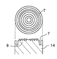
図6は、本実施形態における成形型6の上面図と側面図である。
【0040】
光学機能面8を形成する微細形状は、光学有効径20mmの範囲において、平面上に格子高さ5〜20μm、格子幅0.1〜10mmのブレーズ型回折格子を有し、上面図に示されるように中心への凸形状で同心円状に配置されている。光学有効径外の型成形面には、溝深さ80〜200μm、溝幅0.5〜1mmと光学機能面の格子高さに比べて十分に深い溝形状部7を同心円状に配置する。この溝形状部7は、図13に示されるように、レンズブランクの材質や形状、成形樹脂の特性、さらには成形型の光学機能面形状等を考慮して、その形状や大きさを選択する。具体的には、溝形状部7の断面形状は、図13に示すような台形あるいはV字形等でもよい。
【0041】
図7は、図6に示す成形型により成形された回折光学素子を示す図である。
【0042】
レンズブランク10上に形成された樹脂層の光学機能面8’は、ブレーズ型回折格子の中心への凹形状、即ち上記の成形型の反転形状として同心円状に形成される。回折光学素子の光学有効径外においては、型成形面の溝形状部7の反転形状であるブロック部7’が同心円状に形成される。
【0043】
以下、本実施形態における成形プロセスを図5、図8を参照して説明する。
【0044】
まず、成形型6の成形面上中央付近に不図示のディスペンサーにて紫外線硬化性樹脂11を適量供給し、あらかじめ樹脂との密着力を上げるためのカップリング処理を片面に施したレンズブランク10を、カップリング処理面を下にしてリング状のレンズブランク保持部材9に嵌め込む。この際に、芯だし用チャック等、さらにレンズブランク10を保持するための機構を備えても良い。その後、リング状のレンズブランク保持部材9を下降させ、成形型6とレンズブランク10を相対的に接近させ、紫外線硬化性樹脂11を所望の厚み、かつ光学有効径外の溝形状部7を有する外周まで満たすように充填させる。この時、樹脂11への気泡混入や型成形形状への樹脂未充填を防止するために、樹脂の粘度や型成形面の濡れ性を考慮して、接液速度を調整しなければならない。その後、紫外線照射ランプ12により紫外線を樹脂層に対して照射する。重合硬化が完了した後、リング状のレンズブランク保持部材9を上昇させることで、成形型6から硬化物樹脂11とレンズブランク10から成る回折光学素子を剥離させる。
【0045】
前述したように、ブレーズ型格子が中心への凸形状で同心円状に配置されているこの成形型においては、その離型方向は成形型外周から型中心に向かって進行するのが最も効果的である。しかるに、リング状のレンズブランク保持部材9の上昇によってレンズブランク10の外周部に負荷される離型力は、この外周部にできるだけ均一に負荷されなければならない。よって、成形型6の型上面とリング状のレンズブランク保持部材9の上面はできる限り高精度に平行となるように配置させる。
【0046】
また、成形型外周から進行する離型を型中心において終点とさせるために、図9に示すような押圧部材13をレンズブランク10上に設置しても良い。押圧部材13は不図示の装置により型中心光軸上に上下動自在に保持され、離型時においてはレンズブランク10を適切な力で押圧する。よって、レンズブランク10と樹脂層11を通して押圧部材13が成形型中心を押圧する力が、レンズブランク10の外周部に負荷される離型時応力を型中心へと進行させる。
【0047】
さらに、リング状のレンズブランク保持部材9の駆動機構による上昇スピードは、生産タクトを考慮した上で、できるだけモータ等を用いた連続的で緩やかなスピードに設定するのが良い。また、この駆動機構を油圧式として、リング状のレンズブランク保持部材9の下面を3点以上の作用点で同時同圧に押し上げることで、より均一な離型力を負荷させることができる。
【0048】
しかるに、本実施形態の構成においては、離型時の光学微細形状部に負荷される離型時応力を低下または分散させ、レプリカ離型を高精度に行うことができる。よって、十分な光学的機能を満たした所望形状の回折光学素子を得ることができると同時に、回折光学素子のレプリカ成形における生産性を向上させ、コスト削減を図ることができる。
【0049】
(第2の実施形態)
図10は、第2の実施形態における成形型14の上面図と側面図である。
【0050】
光学機能面8を形成する微細形状は、光学有効径20mmの範囲において、平面上に格子高さ5〜20μm、格子幅0.1〜10mmのブレーズ型回折格子を有し、上面図に示されるように中心への凹形状で同心円状に配置されている。光学有効径外の型成形面には、溝深さ80〜200μm、溝幅0.5〜1mmと光学機能面の格子高さに比べて十分に深い溝部形状7を同心円状に配置する。
【0051】
図11は、この成形型により作製される回折光学素子を示した図である。レンズブランク10上に形成された樹脂層の光学機能面8’は、ブレーズ型回折格子の中心への凸形状、即ち成形型の反転形状として同心円状に形成される。回折光学素子の光学有効径外においては、型成形面の溝形状部7の反転形状であるブロック部7’が同心円状に形成される。
【0052】
図12は、成形型14の離型初期における成形型端部の離型時応力状態を示しており、図中にある符号は図4と同様である。第1の実施形態においては、格子の垂直な側面に対して離型時応力f1’が負荷されたが、本実施形態においては、格子斜面に対して応力f1’が負荷される。よって、本実施形態における離型時応力f1’はさらに緩和され、光学機能面格子の変形や欠損をより防ぐことができる。
【0053】
本実施形態は、第1の実施形態における成形型の形状と作製される回折光学素子の形状が異なるもので、他の構成は同一であるので、その説明を省略する。
【0054】
以上説明したように、上記の実施形態によれば、レプリカ成形用型の光学有効外の成形面に所望の光学機能面における微細形状深さに比べても十分に深い溝または開口形状を設けるという容易な方法により、離型時の光学微細形状部に負荷される離型時応力を低下または分散させ、レプリカ離型を高精度に行うことができる。これにより、回折光学素子のレプリカ成形における生産性を向上させ、コスト削減を図り、かつ十分な光学的機能を満たした所望形状の回折光学素子を得ることが可能となる。
【0055】
【発明の効果】
以上説明したように、本発明によれば、成形品の型からの離型を高精度に行なうことが可能となる。
【図面の簡単な説明】
【図1】従来の離型方法を説明する図である。
【図2】従来の離型方法とその作用を説明する図である。
【図3】本発明の第1の実施形態に係わる成形型とその離型方法の説明図である。
【図4】本発明の第1の実施形態に係わる離型方法とその作用を説明する図である。
【図5】本発明の第1の実施形態に係わる成形型と成形装置の断面図である。
【図6】本発明の第1の実施形態に係わる成形型の断面図と上面図である。
【図7】本発明の第1の実施形態に係わる光学素子の断面図と上面図である。
【図8】本発明の第1の実施形態に係わる成形型と成形装置の断面図である。
【図9】本発明の第1の実施形態に係わる成形型と成形装置の断面図である。
【図10】本発明の第2の実施形態に係わる成形型の断面図と上面図である。
【図11】本発明の第2の実施形態に係わる光学素子の断面図と上面図である。
【図12】本発明の第2の実施形態に係わる離型方法とその作用を説明する図である。
【図13】溝形状部の変形例を示す図である。
【符号の説明】
1 レンズブランク
2 成形用型
3 光硬化性樹脂
4 溝形状部
5 成形用型
6 成形用型
7 成形型の溝形状部
7’ 光学素子の溝形状部
8 成形型の光学機能面
8’ 光学素子の光学機能面
9 レンズブランク保持部材
10 レンズブランク
11 光硬化性樹脂
12 紫外線照射ランプ
13 押圧部材
14 成形用型[0001]
TECHNICAL FIELD OF THE INVENTION
The present invention relates to a molding die for transferring a fine shape having a desired optical function to a surface of a resin material, and an optical element molded by the molding die.
[0002]
[Prior art]
2. Description of the Related Art Conventionally, as one of the molding techniques of a diffractive optical element, there is a replica molding technique which is excellent in large-area moldability and high transferability and is suitable for mass production due to its ease of molding technique. In this replica molding technique, a photocurable resin is dropped on a molding surface of a mold having an inverted shape of a desired optical shape, a lens blank is pressed thereon, and the resin is spread out. The molding is performed by irradiating light from a light source to cure the photocurable resin and releasing the cured resin together with the lens blank.
[0003]
In such mold release in replica molding, the cured resin easily adheres or adheres to the mold surface, or the fine shape is deformed or damaged by the stress at the time of mold release. It is difficult to release well.
[0004]
Therefore, in a replica molding method for molding a diffractive optical element having a desired shape, many mold release methods have been proposed for improving the mold release property and obtaining a high-precision molded article excellent in transferability.
[0005]
As a known technique for improving the releasability, application of a release agent to a molding surface or addition of a release agent to a resin material, which is a general technique, is already known. Further, as a more specific method, Japanese Patent Laid-Open No. 5-50442 discloses a method of applying a dense / dense substance to the outside of the optical effective diameter of the mold or forming a predetermined shape that maximizes the stress at the time of mold release. A method of reducing the initial adhesion between the mold and the molded article by providing the mold has been proposed. Further, in Japanese Patent Application Laid-Open No. 4-144718, a crack is generated in the outer peripheral portion by vertically moving one of an inner mold and an outer mold of a molding die composed of an inner mold and an outer mold that can move up and down, Methods for facilitating demolding have been proposed.
[0006]
[Problems to be solved by the invention]
However, the technology disclosed in the above-mentioned publications may not be applicable to replica mold release of a diffractive optical element having a desired fine shape, and when more precise moldability and efficient productivity are required. The following problems occur.
[0007]
In replica release of a diffractive optical element having a fine shape on a flat or curved optical function surface, deformation or loss of the lattice due to stress at the time of release is inevitable to some extent. In replica release, a stress at the time of release, which is distributed in a complicated manner, is applied to a minute shape portion, and a deformation or a defect is given to a minute lattice portion or the like. Needless to say, these deformations and defective portions significantly reduce the optical performance of the optical element.
[0008]
Therefore, as one of the methods for avoiding this obstacle, there is a method of applying a release agent on the mold molding surface to reduce the adhesion between the mold and the cured resin. Due to a difference in film thickness or dripping, the optical fine shape on the molded surface which has been extremely precisely processed is distorted.
[0009]
On the other hand, in the technique of adding a release agent to the resin material itself, effects such as deterioration of the environmental resistance of the resin material and a decrease in the refractive index are observed, which is not preferable as an optical material for forming a diffractive optical element.
[0010]
Further, in the molding die disclosed in JP-A-5-50442 for reducing the initial adhesive force at the time of replica release, even if the initial adhesive force at the time of release can be reduced, the optical fine shape can be reduced. The effect cannot be obtained up to the stress at the time of mold release applied to the part.
[0011]
Further, in the molding die disclosed in Japanese Patent Application Laid-Open No. 4-144718, not only the stress at the time of mold release imposed on the optical fine shape portion cannot be reduced, but also the production tact time due to the mold operation process. This leads to an increase in the production time and the scale of the production apparatus itself, which not only lowers productivity but also significantly increases costs.
[0012]
Therefore, the present invention has been made in view of the above-mentioned problems, and an object of the present invention is to enable a molded product to be released from a mold with high accuracy.
[0013]
[Means for Solving the Problems]
In order to solve the above-described problems and achieve the object, a molding die according to the present invention is a molding die for transferring a fine shape having a desired optical function to a resin material and molding an optical element. A first molding surface for transferring the fine shape to the resin material; and a first molding surface provided outside the effective range of the first molding surface, the concave shape portion having a depth greater than the depth of the fine shape. 2 molding surface.
[0014]
In the molding die according to the present invention, the fine shape has a light diffraction function as the optical function.
[0015]
Further, in the molding die according to the present invention, the fine shape is constituted by concentric unevenness.
[0016]
Further, in the molding die according to the present invention, the concave portion is formed concentrically with the fine shape outside the effective diameter of the fine shape.
[0017]
Further, in the molding die according to the present invention, the concave portion is formed of a groove having a rectangular cross section.
[0018]
Further, in the molding die according to the present invention, the concave portion has a trapezoidal groove in cross section.
[0019]
Further, in the molding die according to the present invention, the concave portion is formed of a V-shaped groove in cross section.
[0020]
Further, the optical element according to the present invention includes an optical function surface on which a fine shape is formed, and a convex portion which is arranged outside the effective range of the optical function surface and has a height higher than the fine shape. It is characterized by.
[0021]
Further, in the optical element according to the present invention, the fine shape has a light diffraction function as an optical function.
[0022]
BEST MODE FOR CARRYING OUT THE INVENTION
Hereinafter, a preferred embodiment of the present invention will be described.
[0023]
First, an outline of the present embodiment will be described.
[0024]
In this embodiment, a photocurable resin is dropped on a mold surface having an optically desired fine shape, and the photocurable resin is pressed with a flat or curved glass substrate, and irradiated with light to form a diffractive optical element. In a molding die to be molded, a groove or opening shape sufficiently deeper than a fine shape depth on a desired optical function surface is provided on a molding surface outside the optically effective portion of the molding die.
[0025]
In addition, the inverted shape of the concentric or vertical stripe fine shape of the desired diffractive optical element is processed on the molding surface, and the molding of the fine surface of the molding surface with the photocurable resin is performed by the molding die. The molding surface is configured so that it is performed simultaneously with the shape molding with a photocurable resin having a groove or opening shape that is sufficiently deep compared to the fine shape depth in the desired optical function surface provided outside the optical effective surface. I have.
[0026]
Further, the diffractive optical element of the present embodiment is a molded diffractive optical element formed by so-called replica molding in a molding die, and outside the optically effective portion thereof, compared with a fine shape height on a desired optical functional surface. Also, a sufficiently high convex shape is formed.
[0027]
By using the above configuration, the following effects can be obtained. FIG. 1 is a schematic view showing a mold release process of replica molding. A process of applying an external force F and releasing the
[0028]
FIG. 2 shows a stress state at the time of mold release at the left end of the mold in the initial stage of mold release. The component force of the releasing force f applied to the first lattice at the left end by the external force F can be divided into a centripetal force f2 due to the warpage of the
[0029]
The stress that causes deformation or loss of the lattice in the replica release is f1 in the drawing, and the present embodiment shows a configuration in which the stress f1 during release is reduced or dispersed by an easy method.
[0030]
FIG. 3 is a schematic diagram illustrating a mold release process of replica molding according to the configuration of the present embodiment.
[0031]
The external force F after the
[0032]
FIG. 4 shows a stress state at the time of mold release at the left end of the
[0033]
The component force of the releasing force f3 applied to the left end groove shape portion by the external force F can be divided into a centripetal force f5 due to the warpage of the
[0034]
Therefore, the deformation or loss of the optical function surface lattice due to the stress at the time of mold release is reduced, the productivity in replica molding of the diffractive optical element having a fine shape is improved, the cost is reduced, and the sufficient optical function is satisfied. A replica molded product having a desired shape can be obtained.
[0035]
(1st Embodiment)
FIG. 5 is a diagram showing a schematic configuration of a replica molding apparatus according to the first embodiment of the present invention.
[0036]
In FIG. 5,
[0037]
The ring-shaped lens
[0038]
As the UV-
[0039]
FIG. 6 is a top view and a side view of the molding die 6 in the present embodiment.
[0040]
The fine shape forming the
[0041]
FIG. 7 is a diagram showing a diffractive optical element molded by the molding die shown in FIG.
[0042]
The
[0043]
Hereinafter, the molding process in the present embodiment will be described with reference to FIGS.
[0044]
First, an appropriate amount of the ultraviolet
[0045]
As described above, in this mold in which the blazed grating is arranged concentrically in a convex shape toward the center, it is most effective that the mold releasing direction proceeds from the outer periphery of the mold toward the center of the mold. is there. However, the release force applied to the outer peripheral portion of the
[0046]
In addition, a pressing
[0047]
Further, it is preferable that the ascending speed of the ring-shaped lens
[0048]
However, in the configuration of the present embodiment, the replica release can be performed with high precision by reducing or dispersing the release stress applied to the optical fine shape portion during release. Therefore, a diffractive optical element having a desired shape that satisfies a sufficient optical function can be obtained, and at the same time, productivity in replica molding of the diffractive optical element can be improved and cost can be reduced.
[0049]
(Second embodiment)
FIG. 10 is a top view and a side view of the molding die 14 in the second embodiment.
[0050]
The fine shape forming the
[0051]
FIG. 11 is a diagram showing a diffractive optical element manufactured by this mold. The optically functional surface 8 'of the resin layer formed on the
[0052]
FIG. 12 shows a stress state at the time of mold release at the end of the mold at the initial stage of mold release of the
[0053]
This embodiment is different from the first embodiment in the shape of the molding die and the shape of the diffractive optical element to be manufactured, and the other configuration is the same.
[0054]
As described above, according to the above-described embodiment, a groove or an opening that is sufficiently deep compared to the fine shape depth of the desired optical function surface is provided on the molding surface outside the optically effective portion of the replica molding die. An easy method can reduce or disperse the stress at the time of release applied to the optical fine shape portion at the time of release, and perform replica release with high accuracy. As a result, it is possible to improve productivity in replica molding of the diffractive optical element, reduce costs, and obtain a diffractive optical element having a desired shape that satisfies a sufficient optical function.
[0055]
【The invention's effect】
As described above, according to the present invention, a molded product can be released from a mold with high accuracy.
[Brief description of the drawings]
FIG. 1 is a diagram illustrating a conventional mold release method.
FIG. 2 is a diagram illustrating a conventional mold release method and its operation.
FIG. 3 is an explanatory diagram of a mold and a method of releasing the mold according to the first embodiment of the present invention.
FIG. 4 is a diagram illustrating a mold release method according to the first embodiment of the present invention and its operation.
FIG. 5 is a cross-sectional view of a forming die and a forming apparatus according to the first embodiment of the present invention.
FIG. 6 is a cross-sectional view and a top view of a molding die according to the first embodiment of the present invention.
FIG. 7 is a sectional view and a top view of the optical element according to the first embodiment of the present invention.
FIG. 8 is a sectional view of a molding die and a molding apparatus according to the first embodiment of the present invention.
FIG. 9 is a sectional view of a molding die and a molding device according to the first embodiment of the present invention.
FIG. 10 is a cross-sectional view and a top view of a molding die according to a second embodiment of the present invention.
FIG. 11 is a sectional view and a top view of an optical element according to a second embodiment of the present invention.
FIG. 12 is a diagram illustrating a mold release method according to a second embodiment of the present invention and its operation.
FIG. 13 is a view showing a modification of the groove portion.
[Explanation of symbols]
REFERENCE SIGNS
Claims (9)
前記微細形状を前記樹脂材料に転写するための第1の成形面と、
該第1の成形面の有効範囲外に設けられ、前記微細形状の深さよりも深い凹形状部を有する第2の成形面とを具備することを特徴とする成形用型。A molding die for molding an optical element by transferring a fine shape having a desired optical function to a resin material,
A first molding surface for transferring the fine shape to the resin material;
A second molding surface provided outside the effective range of the first molding surface and having a concave portion deeper than the depth of the fine shape.
該光学機能面の有効範囲外に配置され、前記微細形状よりも高さが高い凸形状部とを具備することを特徴とする光学素子。An optical function surface on which a fine shape is formed,
An optical element comprising: a convex portion that is arranged outside an effective range of the optical function surface and that is higher than the fine shape.
Priority Applications (1)
| Application Number | Priority Date | Filing Date | Title |
|---|---|---|---|
| JP2002204394A JP2004042493A (en) | 2002-07-12 | 2002-07-12 | Mold and optical element |
Applications Claiming Priority (1)
| Application Number | Priority Date | Filing Date | Title |
|---|---|---|---|
| JP2002204394A JP2004042493A (en) | 2002-07-12 | 2002-07-12 | Mold and optical element |
Publications (1)
| Publication Number | Publication Date |
|---|---|
| JP2004042493A true JP2004042493A (en) | 2004-02-12 |
Family
ID=31710009
Family Applications (1)
| Application Number | Title | Priority Date | Filing Date |
|---|---|---|---|
| JP2002204394A Withdrawn JP2004042493A (en) | 2002-07-12 | 2002-07-12 | Mold and optical element |
Country Status (1)
| Country | Link |
|---|---|
| JP (1) | JP2004042493A (en) |
Cited By (3)
| Publication number | Priority date | Publication date | Assignee | Title |
|---|---|---|---|---|
| EP2469252A4 (en) * | 2009-08-19 | 2014-12-24 | Hamamatsu Photonics Kk | SPECTROSCOPY MODULE AND METHOD OF MANUFACTURE |
| JP2016206688A (en) * | 2016-08-31 | 2016-12-08 | キヤノン株式会社 | Manufacturing method of diffraction optical element, and diffraction optical element |
| WO2017146203A1 (en) * | 2016-02-25 | 2017-08-31 | コニカミノルタ株式会社 | Method for producing molded resin article, and molded resin article |
-
2002
- 2002-07-12 JP JP2002204394A patent/JP2004042493A/en not_active Withdrawn
Cited By (5)
| Publication number | Priority date | Publication date | Assignee | Title |
|---|---|---|---|---|
| EP2469252A4 (en) * | 2009-08-19 | 2014-12-24 | Hamamatsu Photonics Kk | SPECTROSCOPY MODULE AND METHOD OF MANUFACTURE |
| US9075193B2 (en) | 2009-08-19 | 2015-07-07 | Hamamatsu Photonics K.K. | Spectroscopy module and manufacturing method therefor |
| US9797773B2 (en) | 2009-08-19 | 2017-10-24 | Hamamatsu Photonics K.K. | Spectroscopy module and manufacturing method therefor |
| WO2017146203A1 (en) * | 2016-02-25 | 2017-08-31 | コニカミノルタ株式会社 | Method for producing molded resin article, and molded resin article |
| JP2016206688A (en) * | 2016-08-31 | 2016-12-08 | キヤノン株式会社 | Manufacturing method of diffraction optical element, and diffraction optical element |
Similar Documents
| Publication | Publication Date | Title |
|---|---|---|
| JP5411557B2 (en) | Microstructure transfer device | |
| US7964135B2 (en) | Method and apparatus for imprinting energy ray-setting resin, and discs and semiconductor devices with imprinted resin layer | |
| CN101027138B (en) | Method for forming resin layer, apparatus for forming resin layer, disk, and method for manufacturing disk | |
| JP2006337985A (en) | Method of manufacturing high sag lens and lens manufactured by using the same method | |
| JP2008213210A (en) | Transfer method and optical element manufactured thereby | |
| JP4371777B2 (en) | Resin curing method and resin molded product manufacturing method | |
| JPH02126434A (en) | Optical disk substrate molding method | |
| JP2849299B2 (en) | Manufacturing method of composite precision molded products | |
| JP2003291159A (en) | Resin curing method, manufacturing method for resin molding, etc., appliance used for them, and product to be obtained | |
| JP3731017B2 (en) | Optical device manufacturing method | |
| JP2004042493A (en) | Mold and optical element | |
| JP3239598B2 (en) | Method for manufacturing diffractive optical element | |
| CN100395614C (en) | Light guide plate manufacturing method | |
| JP2009066827A (en) | Optical element molding method | |
| JP2007326330A (en) | Mold for molding composite optical element and composite optical element | |
| JP2800898B2 (en) | Manufacturing method of aspherical optical element | |
| JP2004205924A (en) | Transfer method of fine shape | |
| JP4171936B2 (en) | Resin-molding mold for resin-bonded optical element and manufacturing method | |
| JP5499553B2 (en) | Nanoimprint pattern forming method and substrate used therefor | |
| JP2859695B2 (en) | Method and apparatus for forming aspherical optical element | |
| JP3941478B2 (en) | Manufacturing method of optical waveguide | |
| JP2006113339A (en) | Method for molding diffractive optical element and diffractive optical element molded using the same | |
| JP4419665B2 (en) | Optical element manufacturing method | |
| JP2006110882A (en) | Method for manufacturing composite optical element and composite optical element | |
| JP2010201621A (en) | Method of manufacturing plastic lens, and the plastic lens |
Legal Events
| Date | Code | Title | Description |
|---|---|---|---|
| A300 | Withdrawal of application because of no request for examination |
Free format text: JAPANESE INTERMEDIATE CODE: A300 Effective date: 20051004 |