【発明の名称】発光素子、及び表示装置
【特許請求の範囲】
【請求項1】反射部材と、発光層と、位相差板と、偏光板とをこの順に備える発光素子であって、前記発光層と前記位相差板との間に、偏光分離手段を設け、前記偏光分離手段は、前記発光層の発光波長範囲の一部または全部を含み、なおかつ可視波長範囲よりも狭い波長範囲の光であって、前記発光層側から前記偏光分離手段側へ向かう光のうち、前記位相差板の作用により前記偏光板で吸収される直線偏光に変換される偏光成分は反射し、それ以外の光は透過するものであり、前記反射部材は少なくとも垂直入射した円偏光は回転方向が逆の円偏光として反射する反射面であることを特徴とする発光素子。
【請求項2】前記偏光分離手段がコレステリック液層層であり、前記位相差板が1/4波長板であることを特徴とする請求項1に記載の発光素子。
【請求項3】反射部材と、発光層と、位相差板と、偏光板とをこの順に備える発光素子であって、前記位相差板と前記偏光板との間に、偏光分離手段を設け、前記偏光分離手段は、前記発光層の発光波長範囲の一部または全部を含み、なおかつ可視波長範囲よりも狭い波長範囲の光であって、前記発光層側から前記偏光分離手段へ向かう光のうち、前記偏光板で吸収される直線偏光成分は反射し、それ以外の光は透過する直線偏光分離手段であり、前記位相差板は1/4波長板であり、前記反射部材は少なくとも垂直入射した円偏光を回転方向が逆の円偏光として反射する反射面であることを特徴とする発光素子。
【請求項4】前記発光層が透明電極と金属電極とに挟まれた有機薄膜であり、前記金属電極が前記反射部材を兼ねた反射性の金属電極であることを特徴とする請求項1から請求項3のいずれかに記載の発光素子。
【請求項5】マトリクス状に配置された複数の発光素子と、前記発光素子の発光動作を画像情報に基づいて制御する制御手段を有する表示装置であって、前記発光素子として請求項1から4のいずれかに記載の発光素子を使用したことを特徴とする表示装置。
【請求項6】マトリクス状に配置した複数の画素を構成する発光素子と、該発光素子の発光動作を画像情報に基づいて制御する制御手段を有する表示装置において、前記発光素子は反射部材を兼ねる金属電極と、有機薄膜からなる発光層と、透明電極とを積層した構造の有機エレクトロルミネッセンス素子と、位相差板と、偏光板とをこの順に備える発光素子であって、前記発光層と前記位相差板との間に、偏光分離手段を設け、前記偏光分離手段は、前記発光層の発光波長範囲の一部または全部を含み、なおかつ可視波長範囲よりも狭い波長範囲の光であって、前記発光層側から前記偏光分離手段側へ向かう光のうち、前記位相差板の作用により前記偏光板で吸収される直線偏光に変換される偏光成分は反射し、それ以外の光は透過するものであり、前記反射部材は少なくとも垂直入射した円偏光は回転方向が逆の円偏光として反射する反射面であることを特徴とする表示装置。
【請求項7】前記偏光分離手段がコレステリック液層層であり、前記位相差板が1/4波長板であることを特徴とする請求項6に記載の表示装置。
【請求項8】前記発光層の発光色が画素により異なり、前記偏光分離手段が反射する光の波長範囲が、該発光色に対応して画素により異なることを特徴とする請求項6または7に記載の表示装置。
【請求項9】前記複数の画素を構成する発光層が、それぞれ赤色発光の発光層、緑色発光の発光層、及び青色発光の発光層のいずれかから構成されるカラー表示を行う表示装置であって、該赤色発光の発光層に対応する位置には赤色光を反射する偏光分離手段、該緑色発光の発光層に対応する位置には緑色光を反射する偏光分離手段、該青色発光の発光層に対応する位置には青色光を反射する偏光分離手段をそれぞれパターン形成したことを特徴とする請求項6または7に記載の表示装置。
【請求項10】前記偏光分離手段が前記画素を構成する前記発光層の発光領域に対応してマトリクス状にパターン形成され、前記偏光分離手段のパターンの間にブラックマトリクスが形成されていることを特徴とする請求項6から請求項9のいずれか1項に記載の表示装置。
【請求項11】前記ブラックマトリクスの開口部が、前記画素を構成する前記発光層の発光領域よりも広いことを特徴とする請求項10に記載の表示装置。
【請求項12】前記画素を構成する発光層が白色光を発光する発光層であり、該画素を構成する発光層の発光領域に対応する位置にそれぞれ赤色光を反射する偏光分離手段、緑色光を反射する偏光分離手段、青色光を反射する偏光分離手段をパターン形成し、さらに赤色光を反射する偏光分離手段と偏光板との間には赤色光を透過するカラーフィルターを、緑色光を反射する偏光分離手段と偏光板との間には緑色光を透過するカラーフィルターを、青色光を反射する偏光分離手段と偏光板との間には青色光を透過するカラーフィルターをそれぞれパターン形成したことを特徴とする請求項6に記載の表示装置。
【発明の詳細な説明】
【発明の属する技術分野】
本発明は発光素子とこの発光素子の発光動作を制御して表示を行う表示装置に関し、特に発光層の裏面に光反射部材を有する有機エレクトロルミネッセンス素子などの発光素子と、これを備える表示装置に利用して有効な技術に関するものである。
【従来の技術】
有機エレクトロルミネッセンス素子(以下有機EL素子と称する)は、有機薄膜からなる発光層に電流を注入することにより、電気エネルギーを光エネルギーに変換して発光する素子である。有機EL素子から構成される表示装置は液晶表示装置に代表される非発光型の表示装置とは異なり、自発光型であるためバックライトなどの補助光源が不要なことから、薄型、軽量であり、さらに視野角が広く、表示の応答速度が早いといった特徴を有する。
図19は従来の有機EL素子の一例を示す概略断面図である。この有機EL素子は透明基板400に陽極である透明電極200、ホール輸送層102、発光層100、電子輸送層101、光反射機能を有する金属電極からなる陰極300を順次積層した構造となっている。
陽極である透明電極200と陰極300との間に直流電圧を印加すると、透明電極200から注入されたホールがホール輸送層102を経由して、また、陰極300から注入された電子が電子輸送層101を経由して、それぞれが発光層100に到達し、電子−ホールの再結合が生じて、ここから所定の波長分布を有する発光が生じる。
発光層100から出射した光のうち透明電極200側に向かった光は透明電極200を通過し、透明基板400から出射する。また、陰極300に向かった光は陰極300で反射して、発光層100、透明電極200等を通過して同じく透明基板400から出射する。
従って、このような有機EL素子の発光動作を制御することで表示を行う表示装置では、陰極を反射率の高い電極にして透明電極側から出射する光量を増やすことが、明るい画像を得るために重要である。
ところで、このような素子構造では発光していない状態では、陰極が反射率の高い鏡のような状態であるため、周囲の景色等が写り込み、黒(暗)表示が十分に暗くならない。つまり、周囲が明るい環境下では黒表示が暗くならず、コントラスト比が低下するという課題を生ずる。この課題を解決する方法として透明基板400の光出射面側に円偏光板800を配置した構造が実用化されている。円偏光板は偏光板600と1/4波長板700から構成される。
円偏光板800は以下の通り作用する。周囲から有機EL素子に入射する外光2000は一般に非偏光であり、偏光板600を通過する際、特定の直線偏光は透過し、これと直交する直線偏光は吸収される。偏光板600を透過した直線偏光は1/4波長板700の作用を受けて、円偏光(ここでは例えば右回りの円偏光)となる。1/4波長板700を通過した光は陰極300で反射する際、位相がπずれて回転方向が逆の円偏光(左回りの円偏光)になる。陰極300で反射した光2000Rは再び1/4波長板700に入射し、これを通過する際、その作用を受けて今度は偏光板600で吸収される直線偏光に変換されて、偏光板600で吸収されるため外部には戻らなくなる。つまり、外光の陰極300での反射はカットされるため黒表示が暗くなり、コントラスト比が著しく改善される。このような構造は特表平8−509834号公報、特開平9−127885号公報等に記載されている。
ところで、有機EL素子を用いた表示装置のフルカラー化に関しては、いくつかの方式が提案・実証されている。例えば青色発光素子と蛍光性の色変換層(CCM:color changing mediums)を組み合わせた方式(以下、CCM法)、白色発光と赤色(R),緑色(G),青色(B)の3原色のカラーフィルタを組み合わせた方式(以下、RGB by white法)、3原色(R,G,B)の発光素子からなる画素を直接パターニングする方式(以下、RGB並置型)などが提案されている。
CCM法は青色発光層で発生した光で蛍光性の色変換用蛍光色素層を励起し、青色から緑色、赤色へ変換し3原色発光を得るものである。この方式は色変換効率が低いと素子効率が低くなる。さらに明るい環境下では外光により色変換層が励起されて明るくなり、黒表示が暗くならないためコントラスト比が低下する。
RGB by white法は作成する発光素子が白色の1種類だけなので、製造が最も容易という特長を有するが、カラーフィルターを用いることから、原理的に光の利用効率が1/3以下に低下する。
RGB並置型は同一基板上に3種の素子をそれぞれ作成する必要があるため、製造プロセスがやや複雑になるが、光の損失が最も少なく、発光効率の面からは理想的な方式といわれている。また、RGBのパターニング(塗り分け)については、分子量の低い蛍光色素や金属錯体などのいわゆる低分子系の材料を用いる場合は、シャドウマスクを用いた有機層の真空蒸着によりRGBを微細な塗り分けする技術が提案されている。
また、π共役ポリマーや色素を高分子化した色素含有ポリマーなどのポリマー系の材料を用いる場合は、フォトエッチングでポリイミドの土手を形成することで、画素領域を分離し、インクジェットにより有機材料を印刷することで、RGBを微細な塗り分ける技術が提案されている(情報映像メディア学会誌Vol.54,No8,pp1115〜1120)。
【発明が解決しようとする課題】
円偏光板を備えた従来技術によれば、有機EL素子の光反射機能を有する電極(陰極)での外光反射が円偏光板の作用により低減できるため、明るい環境下でも高いコントラスト比を実現することができる。しかし、発光時は発光層から出射した光の一部が円偏光板で吸収されるため、表示が暗くなるという課題を有する。これは、一般に発光層から出射する光は非偏光であるため、円偏光板を構成する偏光板で少なくとも1/2の光が吸収されるためである。
また、有機EL素子でフルカラーの表示装置を実現する場合、RGB並置型が素子効率の面から最も好ましい。しかし、現状の有機EL素子は色によっては発光の波長範囲が広く、色純度が高いとはいえない。各原色の色純度を高くするためにカラーフィルタを併用するということが考えられるが、この場合はカラーフィルターで光が吸収されるため、光の利用効率が低下して表示が暗くなる。
本発明は上記実状を鑑み成されたもので、その目的は発光層から出射した光を効率良く表示に寄与させることで、明るい表示を実現すると同時に、発光層裏面の電極などの反射部材による外光の反射を低減することで、明るい環境下でも高いコントラスト比の表示を実現する有機EL素子などの発光素子、及びこの発光素子の発光動作を制御して表示を行う表示装置を提供することにある。
さらに、明るさを損なうことなく色純度を高めた発光素子、及びこの発光素子の発光動作を制御して表示を行う表示装置を提供することにある。この他の目的については以下の記述から明らかになるであろう。
【課題を解決するための手段】
上記目的を達成するため本発明の発光素子は、発光層と位相差板との間に偏光分離手段(コレステリック液晶層)を配置する。偏光分離手段は発光層の発光波長範囲の一部または全部を含み、なおかつ可視波長範囲よりも狭い波長範囲の光であって、前記発光層側から前記偏光分離手段側へ向かう光のうち、前記位相差板の作用により前記偏光板で吸収される直線偏光に変換される偏光成分は反射し、それ以外の光は透過するものとする。
また、発光層の裏面側に位置する反射部材は少なくとも垂直入射した円偏光は回転方向が逆の円偏光として反射する反射面とする。発光層から出射した光のうち、従来、偏光板で吸収されていた偏光成分は偏光板で吸収される前に偏光分離手段で反射して、反射部材へ向かう。偏光分離手段で反射し、反射部材へ向かう光は円偏光であり、反射部材での反射により偏光分離手段を透過する円偏光、すなわち、位相差板の作用により偏光板を透過する直線偏光に変換される円偏光となるため、偏光板で吸収されることなく利用される。
つまり、従来、発光層から出射し、偏光板で吸収され、無駄となっていた光を偏光板で吸収される前に偏光分離手段で反射して、再利用することで発光素子を明るくすることができる。
【発明の実施の形態】
即ち、上記目的を達成するため本発明の発光素子は、発光層とこの発光層の裏面に配置した光反射部材とを有する発光素子において、前記発光層の表面側に発光層から出射する光に対応した所定の波長範囲の光を反射と透過により2種類の円偏光成分に分離する偏光分離手段と、位相差板と偏光板とを配置したものである。
偏光分離手段としては例えばコレステリック液晶層を用いることができ、この際、コレステリック液晶層の選択反射の波長範囲は、発光層の発光波長範囲と同じ、或いはこれよりも狭くする。また、位相差板としては1/4波長板を用いる。
この構造の発光素子では発光層から出射した光は直接、あるいは発光層の裏面に配置した反射部材で反射した後、偏光分離手段を構成するコレステリック液晶層に入射する。コレステリック液晶層に入射した光は、コレステリック液晶の選択反射により一方の回転方向の円偏光(例えば、ここでは左回りの円偏光)成分は反射し、これとは逆回りの円偏光(右回りの円偏光)成分は透過する。コレステリック液晶層を透過した光は位相差板の作用により円偏光から直線偏光に変換され、偏光板で吸収されることなく透過して観察者へ向かう。
一方、コレステリック液晶層で反射した光は、発光層裏面の反射部材で反射して再びコレステリック液晶層に向うが、反射部材での反射の際、位相がπずれて回転方向が逆の円偏光(右回りの円偏光)となる。このため今度はコレステリック液晶層を透過して位相差板の作用により、偏光板を透過する直線偏光に変換された後、偏光板を透過して観察者へ向う。つまり、従来、偏光板で吸収され、無駄となっていた光を偏光板で吸収される前に偏光分離手段(コレステリック液晶層)で反射して、再利用することで発光素子を明るくすることができる。
さらに偏光分離手段(コレステリック液晶層)で反射して再利用される光の波長範囲が、発光層の発光波長範囲よりも狭ければ、実際に素子から出射する光の波長分布は発光層の発光波長分布よりも急峻な分布になるため、発光層の発光自体よりも色純度の高い色光となる。
また、明るい環境下において発光素子に入射する外光は一般に非偏光であるため、偏光板を通過する際、少なくともその半分が吸収される。偏光板を通過した光は位相差板を透過する際、その作用を受け、円偏光(例えば右回りの円偏光)となりコレステリック液晶層を透過する。コレステリック液晶層を透過した光は反射部材で反射する際、回転方向が逆の円偏光(左回りの円偏光)となり、再びコレステリック液晶層に入射する。コレステリック液晶層に入射した光のうち、選択反射波長以外の波長の光はそのまま透過して、位相差板の作用を受けて偏光板で吸収される直線偏光となり、偏光板で吸収されるため外部には透過しない。
一方、選択反射波長に相当する波長の光はコレステリック液晶層で反射して、再び反射部材でも反射した後、コレステリック液晶層、位相差板、偏光板を通過して外部に出る。この光はわずかなため明るい環境下であっても、黒(暗)表示が暗くなり高いコントラスト比が実現できる。
以下、本発明の具体的な実施例を参照図面により説明する。図1は本発明の発光素子の基本構成と動作原理を説明するための概略断面図である。図1に示す通り、本発明に係る発光素子24は図示しない基板上に形成された透明電極200からなる陽極と、鏡面反射手段を兼ねる陰極300と、陽極と陰極の間に形成した有機層110とから構成される有機EL素子150と、有機EL素子150の透明電極200側に順に配置した偏光分離手段500と、位相差板700と、偏光板600とから構成される。
有機EL素子150の有機層110は陽極(透明電極200)と陰極300との間に陰極300側から順に電子輸送層101、発光層100、ホール輸送層102を積層配置したものを用いることができる。
尚、発光層100と電子輸送層101は兼用できる材料を用いることで1層としても良い。また、有機EL素子150の構造としては、この他に陽極(透明電極200)とホール輸送層102の間に陽極バッファ層を配置したものを用いてもよい。陽極バッファ層としてはCuPcを用いることができる。CuPcは陽極とホール輸送層のコンタクトを向上する役割を果たすものと考えられる。
陽極(透明電極200)には仕事関数の高い透明な電極材料を用いれば良く、例えばITO(Indium Tin Oxide)が好適である。また、将来的にはInZnOを用いることができるようになるであろう。
陰極300には仕事関数の低いAl,Mg,Mg-Ag合金やAl-Li合金などを用いることができる。Al単体では駆動電圧が高く、寿命が短いことから有機層との間に極薄いLi化合物(酸化リチウムLi2O ,LiFフッ化リチウムなど)を挿入してAl−Li合金に匹敵する特性を得るようにしたものを用いても良い。
また、陰極に接する部分の有機層をリチウムやストリンチウムなどの反応性の高い金属でドーピングして、駆動電圧を低くするようにしても良い。尚、陰極300は光の反射率が高い材料から構成されることが、発光層から出射した光の利用効率向上の面から望ましい。
さらに、陰極300は後述する理由から少なくとも垂直入射した円偏光を回転方向が逆の円偏光として反射する鏡面であることが、外光反射の低減、及び発光層から出射した光の利用効率向上という面から望ましい。
有機層110は陽極(透明電極200)と陰極300との間に所定の電圧が印加されたとき所望の色で発光する材料を用いる。
赤色発光用の材料としては、例えばホール輸送層102はα−NPD( N、N'−ジ(α−ナフチル)−N、N'-ジフェニル1、1'−ビフェニル−4、4'−ジアミン)や、トリフェニルジアミン誘導体TPD(N,N'−ビス(3−メチルフェニル)1,1'−ビフェニル−4,4'−ジアミン)、電子輸送性発光層(電子輸送層101と発光層100を兼用)は、Alq3「トリス(8−キノリノレート)アルミニウム)」にDCM−1「4−(ジシアノメチレン)−2−メチル−6−(p−ジメチルアミノスチリル」−4H−ピランを分散したものを用いることができる。
緑色発光用の材料としては、例えばホール輸送層102はα-NPDや、トリフェニルジアミン誘導体TPD、電子輸送性発光層(電子輸送層101と発光層100を兼用)はAlq3や、Bebqや、キナクリドンでドーピングしたAlq3を用いることができる。
青色発光用の材料としては、例えばホール輸送層102はα−NPDや、トリフェニルジアミン誘導体TPD、発光層100はDPVBi「4,4’−ビス(2,2−ジフェニルビニル)ビフェニル」や、これとBCzVBi「(4,4’−ビス(2−カルバゾールビニレン)ビフェニル」からなる材料、或いはジスチリルアリレーン誘導体をホストとし、ジスチリルアミン誘導体をゲストとしてドーピングしたもの、電子輸送層102としてはAlq3を用いることができる。
また、電子輸送性発光層(電子輸送層101と発光層100を兼用)として、Zn(oxz)2「2−(o−ヒドロキシフェニル)−ベンズオキサゾールの亜鉛錯体」を用いることができる。
さらに、上記低分子系の材料の他にポリマー系の材料を用いることができる。ポリマー系の材料としてはPEDT/PSS(Polyethylene dioxythiopheneとPolystyrene sulphonateの混合層)とPPV「(Poly(p−Phenylene Vinylene)」の積層膜をホール輸送層102、発光層として用いることができる。また、緑色の発光はPPVに緑インクを調合したもの、赤色の発光は緑インクに赤発光ドーパントとしてローダミン101を添加調合したもので実現でき、青色の発光層としてはF8「Poly(dioctylfluorene)」を用いることができる。尚、F8は電子輸送層101としても機能する。
また、ポリマー系の材料としてはこの他にPVK(ポリビニルカルバゾール)のような色素含有ポリマーを用いることができる。
いずれにしても有機層110を構成する各層は数十nm程度と薄く、これを透過する光の偏光状態はほぼ維持されるものである。
以上から構成される有機EL素子150では、陽極である透明電極200と陰極300とに直流電源900を接続し、透明電極200と陰極300との間に直流電圧を印加すると、透明電極200から注入されたホールがホール輸送層102を経由して、また、陰極300から注入された電子が電子輸送層101を経由して、それぞれが発光層に到達し、電子-ホールの再結合が生じてここから所定の波長の発光が生じると考えられるものである。
透明電極200の有機層110とは反対側には順に偏光分離手段500、位相差板700、偏光板600が積層配置される。偏光分離手段500は所定の波長範囲の光を反射と透過により、2種類の円偏光成分に分離する機能を有するものである。偏光分離手段500としてはコレステリック液晶層が好適である。
コレステリック液晶層はヘリカルな分子配列に基づく特異な光学特性を示すもので、ヘリカル軸に平行に入射した光はコレステリック螺旋のピッチに対応する波長において、螺旋の回転方向に応じて一方の回転方向の円偏光成分は反射し、他方は透過するという選択反射を示すものである。
コレステリック液晶層による選択反射の中心波長λ0と、その波長帯域Δλはそれぞれ式(1)、式(2)で表される。
λ0=nm・p …(1)
Δλ=Δn・p …(2)
ここで、pはコレステリック液晶層の螺旋ピッチ、nmは液晶の平均屈折率、Δnは液晶の複屈折であり、液晶分子の長軸に平行及び垂直な方向の屈折率をそれぞれne、nOとするとnmと、Δnはそれぞれ式(3)、式(4)で表される。
nm=√((ne 2+nO 2)/2) …(3)
Δn=ne−nO …(4)
ここで、例えば、複数の発光素子24を整列配置し、これらの発光動作を制御してフルカラー表示を行う表示装置を実現しようとする場合、発光素子24を構成する有機EL素子150の発光のピーク波長(最大強度となる波長)は、赤色(R),緑色(G),青色(B)の3原色に対応したものとするとよい。つまり、画素毎に有機EL素子150の発光のピーク波長を3原色に対応させて異なったものとする。これに対応してコレステリック液晶層の選択反射の波長範囲、あるいは選択反射の中心波長λOを有機EL素子150の発光波長範囲や発光のピーク波長に対応させる。
図2はコレステリック液晶層に非偏光の光を入射した場合のコレステリック液晶層における透過率の波長依存性を示すグラフであり、それぞれR,G,Bの3原色に対応した選択反射の一例を示したものである。
例えば有機EL素子150の発光色が青色の場合は偏光分離手段500として、図2で示すB反射の特性を示すコレステリック液晶層を配置すれば良い。つまり、偏光分離手段500は有機EL素子150の発光色に対応した選択反射の波長範囲を有するコレステリック液晶層で構成するようにすれば良い。
位相差板700及び偏光板600は従来技術において、所謂円偏光板を構成するものである。つまり、偏光板600はこれを通過する光のうち特定の直線偏光は透過し、これと直交する直線偏光は吸収するものである。
また、位相差板700は偏光板600を通過した直線偏光を、円偏光に変換する1/4波長板として機能するものを用いる。偏光板600は延伸させたポリビニルアルコールにヨウ素を吸収させて、偏光機能を付与した膜の両面にトリアセチルセルロースの保護層を施したものを用いることができる。
位相差板700は透明な一軸延伸した高分子フィルム、例えばポリビニルアルコール、ポリカーボネート、ポリサルフォン、ポリスチレン、ポリアリレート等を用いることができる。尚、一般に位相差板を構成する透明体には屈折率の波長依存性(波長分散)があるため、太陽光や照明光などの外光のように波長範囲が広い光に対しては、一種類の位相差板では十分な性能が得られない。このため波長分散の異なる2種類の位相差フィルムを、その光学軸をずらして張り合わせ、広い波長範囲で1/4波長板として機能する位相差板を構成するようにしてもよい。
尚、偏光板600を透過し、位相差板700を通過した光の円偏光の回転方向が、偏光分離手段500を構成するコレステリック液晶層が選択反射を示す円偏光(例えば左回りの円偏光)とは、逆回りの円偏光(右回りの円偏光)となるように位相差板700の遅相軸の向きを決定することが重要である。
次に本発光素子の動作を図1により説明する。
透明電極200と陰極300とに直流電源900を接続し、電流を流すと発光層100から所定の波長の発光が生じる。発光層100から出射した光のうち透明電極200側に向かった光1000は、そのまま透明電極200を透過して偏光分離手段500に入射する。また、発光層100から出射した光のうち陰極300側に向かった光1001は、陰極300で反射した後、同じく透明電極200を透過して偏光分離手段500に入射する。
この際、発光層100から出射した光は非偏光であるため、偏光分離手段500に入射する光は偏光分離手段500であるコレステリック液晶層の選択反射により、一方の回転方向の円偏光(例えば、ここでは右回りの円偏光)成分は透過し、これとは逆回りの円偏光(左回りの円偏光)成分は反射する。
偏光分離手段500を透過した光1002は、位相差板700の作用により偏光板600を透過する直線偏光に変換され、偏光板600を透過して観察者1000の方向へ向かう。
一方、偏光分離手段500で反射した光1003は、陰極300で反射して再び偏光分離手段500に向かうが、陰極300での反射の際、位相がπずれて回転方向が逆の円偏光(右回りの円偏光)となるため、今度は偏光分離手段500を透過する。偏光分離手段500を透過した光1003は、位相差板700の作用により偏光板600を透過する直線偏光に変換され、偏光板600を透過して観察者1000の方向へ向う。
従って、発光層100から出射した光は、大部分が偏光板で吸収されることなく、観察者1000に向う。つまり、従来、偏光板で吸収され、無駄となっていた光を有効に再利用することで、発光素子の輝度が向上するという効果がある。
また光取出方法としては偏光分離手段500を透過した光1002と偏光分離手段500で反射した光1003とを取り出すことができるので、光の効率が良い。
次に、明るい環境下で周囲から発光素子24に入射する外光について説明する。周囲から発光素子24に入射する外光3000は一般に非偏光であるが、偏光板600を通過する際に所定の直線偏光は吸収され、これと偏光面が直交する直線偏光は透過する。偏光板600を透過した直線偏光は位相差板700の作用を受け、円偏光(ここでは例えば右回りの円偏光)となる。
位相差板700を通過した光は偏光分離手段500を透過して、陰極300で反射する際、位相がπずれて回転方向が逆の円偏光(左回りの円偏光)になる。陰極300で反射した光は偏光分離手段500に入射するが、偏光分離手段500であるコレステリック液晶層における選択反射における波長範囲以外の波長の光3001は、そのまま透過し、選択反射の波長範囲に相当する波長の光は反射する。偏光分離手段500を透過した光(左回りの円偏光)は、位相差板700の作用を受けて偏光板600で吸収される直線偏光となり、偏光板600で吸収されるため外部には戻らない。
一方、偏光分離手段500で反射した光3002は、陰極300で反射して再び偏光分離手段500に向かうが、陰極300での反射の際、位相がπずれて回転方向が逆の円偏光(右回りの円偏光)となるため、今度は偏光分離手段500を透過する。偏光分離手段500を透過した光3002(右回りの円偏光)は、位相差板700の作用により、偏光板600を透過する直線偏光に変換され、偏光板600を透過して観察者1000の方向へ向う。
つまり、発光素子24に入射した外光3000は、まずそのうちの少なくとも半分が偏光板600で吸収される。更に偏光板600を透過した光は陰極300で反射して、偏光分離手段500に入射するが、このうち偏光分離手段500を透過した光3001は偏光板600で吸収される。従って、外部へ出射する光は偏光分離手段500の選択反射の波長範囲に相当するわずかな光3002のみである。
つまり、本発明の発光素子では明るい環境下であっても、外光の大部分がカットされるため、黒表示が暗くなり高いコントラスト比が実現できるという効果がある。
尚、図2に例示した通り、偏光分離手段500を構成するコレステリック液晶層の選択反射の波長分布は、一般に急峻な分布をしており、選択反射の波長範囲は採用する液晶のΔnと螺旋ピッチpにより、有機EL素子の発光の波長範囲よりも小さくすることが可能である。
ここで、一般に発光の中心波長が同じであっても、発光の波長範囲が広く、なだらかな波長分布の場合には、色純度(色度図上での白色光源からの距離の比)が低くなる。従って、偏光分離手段500で反射して再利用される光の波長範囲を、発光層の発光の波長範囲よりも狭く、急峻な分布にすれば、実際に素子から出射する光の波長分布は、発光層の発光波長分布よりも狭く、急峻になるため、発光層からの発光よりも色純度を高くすることができる。
つまり、本発明の発光素子では有機EL素子150自体の発光の色純度に対して、偏光分離手段500で反射して再利用される光の分だけ、色純度を高くすることができるという効果がある。
また、この発光素子を複数整列配置し、個々の発光素子の発光動作を制御して表示を行う表示装置の場合には、R,G,Bの3原色に対応する発光素子の色純度をそれぞれ高めることで、表色範囲の広い表示装置が実現できるという効果もある。
さらに、明るい環境下での外光の反射は、偏光分離手段500であるコレステリック液晶層の選択反射の波長範囲が狭ければ、小さくなるためより高いコントラスト比が得られるという効果がある。
図3及び図4はそれぞれ本発明に係わる発光素子の出射光の相対強度と波長の関係を示すグラフと、色度を示すxy色度図であり、青色発光の有機EL素子150に、偏光分離手段500として図2で例示した青色の波長に選択反射の波長範囲(B反射)を有するコレステリック液晶層を用いた場合の結果である。また、両図とも比較のため、同じ有機EL素子を用い円偏光板を配置した従来方式の結果を併記し、さらに図4には参考のためNTSCの色度を併記した。
図3に示す通り、本発明では従来偏光板で吸収されていた光を再利用することで、光の強度が増加する。特に、青色の光として有効な波長範囲の光の強度が増加しており、図4の色度図に示す通り、色純度は従来(54%)から3%向上し、色度がNTSCの青色の値により近づいている。また、本実施例では輝度が従来の約1.5倍に向上した。
図5及び図6は同じく本発明における発光素子の光の相対強度と波長の関係を示すグラフと、色度を示すxy色度図であり、緑色発光の有機EL素子150に、偏光分離手段500として図2で例示した緑色の波長に選択反射の波長範囲(G反射)を有するコレステリック液晶層を用いた場合の結果である。また、両図とも比較のため、同じ有機EL素子を用い円偏光板を配置した従来方式の結果を併記し、さらに図6には参考のためNTSCの色度を併記した。
図5に示す通り、本発明では従来偏光板で吸収されていた光を再利用することで光の強度が増加する。特に、緑色の光として有効な波長範囲の光の強度が増加しており、図6の色度図に示す通り、色純度は従来(94.5%)から1.5%向上し、色度がNTSCの緑色の値に近づいている。また、本実施例では輝度が従来の約1.6倍に向上した。さらに、明るい環境下(垂直照度180lxの条件)でのコントラスト比は有機EL素子150単体の場合が19であるのに対し、本発光素子では36に向上した。
赤色に関しても赤色発光の有機EL素子150に偏光分離手段500として、赤色の波長に選択反射の波長範囲を有するコレステリック液晶層を用いることで、青色、緑色と同様、色純度の向上、輝度の向上といった効果が得られる。
尚、有機EL素子150の発光の波長範囲と、偏光分離手段500を構成するコレステリック液晶層の選択反射の波長範囲との関係が本発明の発光素子では重要である。
つまり、重視する特性によってその関係を変えても良い。例えば、色純度と明るい環境下でのコントラスト比を重視する場合は、有機EL素子150の発光の波長範囲よりも、偏光分離手段500を構成するコレステリック液晶層の選択反射の波長範囲を狭くすることが望ましい。この場合、選択反射の波長範囲が狭ければ狭いほど外光の反射が減り、コントラスト比は向上するが、その分輝度の向上効果が減るので、使用環境(想定される周囲の明るさ)を考慮した上で、選択反射帯域を決定するようにすると良い。
また、絶対的な輝度を重視する場合は有機EL素子150の発光の波長範囲と、偏光分離手段500を構成するコレステリック液晶層の選択反射の波長範囲を略一致させ、再利用できる光量を最大にすることが有効である。
コントラスト比と輝度を両立するには、有機EL素子の発光の波長範囲を狭くした上で、有機EL素子150の発光の波長範囲と偏光分離手段500を構成するコレステリック液晶層の選択反射の波長範囲を略一致させる。ここで、有機EL素子の発光の分布を半値幅が75nmのガウス型と仮定して計算すると、R,G,Bともに十分な色度(色純度)が得られる(映像メディア学会誌Vol.54,No8,p1116)。従って、コントラスト比と輝度を両立するには有機EL素子の発光波長の半値幅と、偏光分離手段500を構成するコレステリック液晶層の選択反射波長の半値幅を75nm以下とすると良いだろう。
尚、偏光分離手段500であるコレステリック液晶層にR,G,Bで同じ液晶材料を使用する場合、選択反射の波長範囲は原理的に選択反射の中心波長が長くなるほど広くなる。つまり、赤色光に対応したコレステリック液晶層は青色や緑色に対応したコレステリック液晶層に比べて、原理的に選択反射の波長範囲が広くなりコントラスト比の向上効果や、色純度の向上効果が小さくなる。
従って、この場合には赤色光に対応したコレステリック液晶層の選択反射の中心波長は、有機EL素子の発光ピーク波長あるいは中心波長より長波長側に設定して可視波長範囲における選択反射の波長範囲が、有機EL素子の発光の波長範囲と略一致するようにすると良い。
尚、本発明は発光層の裏面に反射部材を有する発光素子において、この前面に偏光分離手段と、位相差板と、偏光板とを配置したものであり、この要件を満たすものであれば、上記実施例に記載のない構成であっても同様な効果が得られることは明らかであろう。
(表示装置の実施例1)
次に本発明の発光素子を複数整列配置し、これら複数の発光素子の発光動作を制御して表示を行う表示装置について説明する。図7は本発明にかかる表示装置1の全体のレイアウトを模式的に示すブロック図であり、図8はその表示部2に構成されたアクティブマトリクスの等価回路図である。
図7に示すように,表示装置1は、基板6のほぼ中央部に表示部2が設けられる。表示部2の上側には、データ線7に対して画像信号を出力するデータ駆動回路3、左側にはゲート線8に対して走査信号を出力する走査駆動回路4が設置されている。これらの駆動回路3,4はNチャネル型とPチャネル型のTFT(Thin Film Transistor)による相補型回路から構成されるシフトレジスタ回路,レベルシフタ回路,アナログスイッチ回路などから構成される。
表示装置1では、液晶表示装置のアクティブマトリクスと同様、第1の基板6上に複数のゲート線と、該ゲート線の延在方向に対して交差する方向に延在させた複数のデータ線が設けられており、図8に示すようにそれらのゲート線G1,G2,…,Gmとデータ線D1,D2,…,Dnとの交差するところにマトリクス状に画素20が配置される。
各画素は発光素子24と、蓄積容量23と、ゲート電極がゲート線に接続し、ソース・ドレイン電極の一方がデータ線に接続され、他方が蓄積容量23に接続されているNチャネル型のTFTからなるスイッチトランジスタ21と、ゲート電極が該蓄積容量23に接続し、ソース電極が上記データ線と同じ方向に延在する共通電位線9に接続され、ドレイン電極が発光素子24を構成する有機EL素子の一方の電極(陰極)に接続されているNチャネル型のTFTからなるドライバトランジスタ22とから構成されている。
また、発光素子24を構成する有機EL素子の他方の電極(陽極)は、画素共通の電流供給線に接続されて一定の電位Vaに保たれる。発光素子24はR,G,Bのいずれかの色光を発するものが、所定の順序でマトリクス状に配置される。
上記構成によれば、走査信号によってスイッチトランジスタ21がオン状態になると、データ線から画像信号がスイッチトランジスタ21を介して蓄積容量23に書き込まれる。従って、ドライバトランジスタ22のゲート電極は、スイッチトランジスタ21がオフ状態になっても、蓄積容量23により画像信号に相当する電位に保持される。
ドライバトランジスタ22は、定電流性に優れるソース接地モードでの駆動状態に保たれ続けて,電流供給線からの電流が発光素子24を構成する有機EL素子を流れるので、発光素子24は発光状態に維持される。このときの発光輝度は、蓄積容量23に書き込まれるデータに依存する。発光の停止は,ドライバトランジスタ22をオフ状態とすることで実現する。
次に図9及び図10を用いて表示装置1の構造を説明する。図9は表示装置1における画素部の平面構造の一部概略図を示し、図10は図9上のA−A’に沿った断面構造を示す。ガラスなどの平坦な第1の基板6上に、スイッチトランジスタ21,ドライバトランジスタ22を形成するための島状のシリコン膜が形成され、その表面にゲート絶縁膜が形成されている。ゲート絶縁膜上には,ゲート電極,ゲート線,蓄積容量用電極が形成され、その後ゲート電極に自己整合的にソース・ドレイン領域が形成されている。さらに第1の層間絶縁膜50が設けられ、コンタクトホールを介してデータ線,共通電位線,蓄積容量用電極が形成されている。
さらに第2の層間絶縁膜51と絶縁材料からなる平坦化膜52が積層形成され、その上に発光素子24の陰極300となる光反射機能を有する電極がしま状にパターン形成されている。陰極300は第2の層間絶縁膜51及び平坦化膜52のコンタクトホールを介してドライバトランジスタ22のドレインと接続されている。平坦化膜52の上には、陰極300が形成された領域を取り囲むように光吸収性の黒色顔料を分散した感光性樹脂材料からなる隔壁60が形成されている。隔壁60はフォトリソグラフィ法により形成される。
陰極300にはR,G,Bいずれかの色に発光する発光層を有する有機層110が所定の配置でパターン形成される。有機層110は上述の構成及び材料から選択すれば良い。有機層110のパターニングは有機層110が低分子系の場合には、公知のシャドーマスクによる真空蒸着有機膜のパターニング成膜技術(例えばS.Miyaguchi,et al,"Organic LED Fullcolor Passive−matrix Display", Journal of the SID,vol.7, No.3,pp221−226(1999)に記載)を用いれば良い。この工程の際、隔壁60はシャドウマスクの突き当て部材として使用することができる。
また、有機層110をポリマー系の材料で構成する場合は公知のインクジェットパターニング技術(例えば、T.Shimoda,et al "Multicolor Pixel Patterning of Light−Emitting Polymers by Ink−Jet Printing",SID99, Digest,pp.376(1999)に記載)を用いれば良い。この工程の際、隔壁60は画素領域を分離する土手として機能する。
有機層110の上には対向電極である陽極(透明電極200)が全面的に形成されている。透明電極200は図示しない電流供給線と接続される。透明電極200の上には透明な絶縁材料からなる平坦化膜70が形成される。平坦化膜70は透明電極200を保護すると同時に、この上に配置する部材の積層を容易にするためのものである。
平坦化膜70としては透明なアクリル系樹脂、カルド系樹脂、ベンゾシクロブテン樹脂、ポリイミド系樹脂等の有機材料を用いれば良い。これらの有機材料はスピンコート法などで成膜することで、その表面が比較的容易に平坦化できる。
平坦化膜70の上には光学的に等方で透明かつ平坦な基板からなる第2の基板90が配置される。
第2の基板90には一方の面にブラックマトリクス層(BM層)80と偏光分離手段500が形成され、他方の面に位相差板700と偏光板600が積層配置されている。第2の基板90は偏光分離手段500が形成された面が、第1の基板6の有機層110形成面と対向するように配置する。第2の基板90上に形成された偏光分離手段500は、有機層110の発光層の発光色に対応した選択反射の波長範囲を有するコレステリック液晶層がパターン形成されており、コレステリック液晶層の選択反射の波長範囲と有機層110における発光の波長範囲の関係は上記説明の通りとする。
第1の基板6と第2の基板90はパターン形成された有機層110の位置と、パターン形成されたコレステリック液晶層の位置が略一致するように重合せて、透明粘着材により全面を密着するか、表示部の周囲を枠状のシール材でシールし,窒素を封入して、密閉接着する。
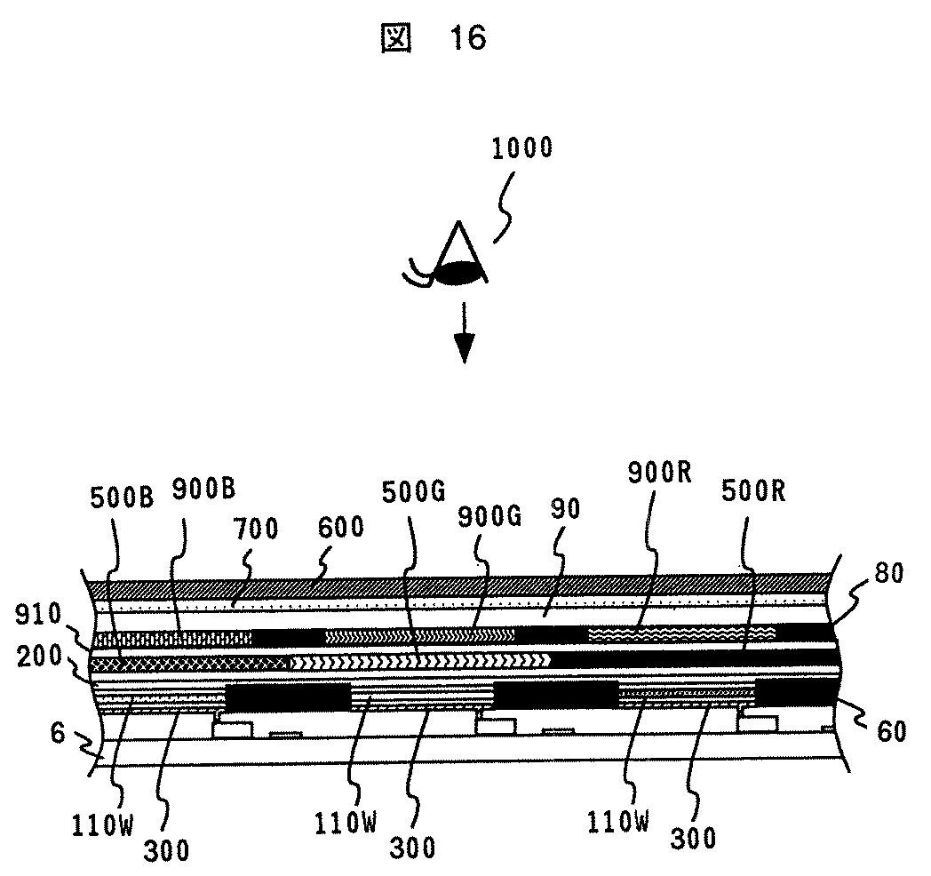
図11は表示装置1の一部断面を示す概略構成図である。また、図12は表示装置1の一部正面図である。図11に示す通り、赤色(R)発光の有機層110Rの上には、赤色に対応した選択反射の波長範囲を有するR反射のコレステリック液晶層500Rを、緑色 ( G ) 発光の有機層110Gの上には緑色に対応した選択反射の波長範囲を有するG反射のコレステリック液晶層500Gを、青色(B)発光の有機層110Bの上には青色に対応した選択反射の波長範囲を有するB反射のコレステリック液晶層500Bを配置する。
また、図12に示す通り、第2の基板90に形成したBM層80は第1の基板6に形成された隔壁60よりも小さく形成する。これは、BM層80を隔壁よりも小さくすることで有機層110からの発光がBM層80で遮られて表示が暗くなることを避けるためであり、位置合わせの際のマージンを確保するためでもある。
次に第2の基板90のBM層80及び偏光分離手段500の形成方法について説明する。
BM層80としては液晶表示装置に使用されているものと同様、金属クロム、酸化クロム、カーボンブラックなどの遮光性顔料を分散させた感光性樹脂を用いることが出来る。本発明の発光素子では特にBM層に外光反射の低減による画質の向上(明環境下での高コントラスト比の維持)が要求されるため、低い反射率が要求される。この要求からBM層としては最も反射率が低くできる遮光性顔料を分散させた感光性樹脂を用いたものが望ましい。
しかし、本発明の発光素子ではBM層80より外側、つまり観察者側には位相差板700と偏光板600が配置され、これらが円偏光板として機能するため反射率が高い金属クロムであっても、金属クロムでの外光反射は抑制されるため使用してもかまわない。
次に第2の基板90にBM層80を形成する工程の一例を説明する。図13は遮光性顔料を分散させた感光性樹脂によるBM層80の形成工程の説明図である。
(a)まず光学的に等方で透明、かつ平坦な第2の基板90上にカーボンブラックを分散したネガ型感光性樹脂85をスピンコーターやダイコーターなどにより塗布する。この際、第2の基板90上にあらかじめ密着性を向上させる薄膜を形成しておいても良い。
第2の基板90としてはガラスの他、キャスティング法(溶液流延法)により成膜したポリカーボネートフィルムや、トリアセチルセルロースフィルム等のポリマーフィルム、或いは射出成形により形成した脂環式アクリル樹脂(商品名オプトレッツ:日立化成製)等の光学的に等方なプラスチックシートやプラスチックフィルムなどを用いることができる。
(b)次に塗布された層をホットプレートなどを用いて仮硬化し、ネガ型感光性樹脂85の感度に合致した波長を有する露光装置により所定のパターンを有するマスク86を用いて露光する。(c)その後、現像することで露光された部分がBM層80として残り、マスクにより遮光された部分は溶出し、基板面が露出する。(d)引き続き洗浄、乾燥を行い、アクリル樹脂、あるいはポリイミド系樹脂などの透明樹脂を塗布して、表面を平坦化する平坦化膜88を構成する。
次にBM層80が形成された第2の基板90にコレステリック液晶層からなる偏光分離手段500を形成する方法の例を説明する。
面内にR,G,Bに対応した選択反射の波長範囲を有するコレステリック液晶層を形成する方法は、公知の技術を用いればよく、例えば異なる液晶材料を印刷する方法や、液晶ポリマーを一面に塗工してから何らかの方法でR反射,G反射,B反射をパターン形成する方法がある。
液晶ポリマーを一面に塗工してから何らかの方法でR,G,Bをパターン形成する方法としては、選択反射波長の温度依存性を利用して温度を変えながら、架橋により構造を固定する方法「例えばR.Maurer,etale,SID94, Digest,pp399−402(1994)に記載」や、選択反射波長を光照射により制御する方法(例えば特開2000−147236号公報)などがある。
面内にR,G,Bに対応した選択反射の波長帯域を有するコレステリック液晶層をパターン形成する方法は、所望の選択反射が得られる領域がパターン形成される方法であれば、いずれの方法であっても良い。
図14はBM層80が形成された第2の基板90にパターン形成されたコレステリック液晶層からなる偏光分離手段500を、形成する方法の一例を説明するための図である。
ここでは選択反射波長を光照射により制御する方法について説明する。この方法は、シッフ塩基を介して光学活性基を結合したモノマーユニットを一成分とする側鎖型液晶ポリマーに光酸発生剤を添加した系において、紫外線照射により光学活性基を切断することで選択反射波長を制御する方法である。つまり、液晶ポリマー(共重合体)は光学活性基を含有するモノマー単位の含有率に基づいて、コレステリック液晶の螺旋ピッチが変化し、選択反射波長は当該ピッチで決定されるため、前記含有率の制御で選択反射波長を制御する方法である。光学活性基を含有するモノマー単位の含有率が高いほどピッチが小さくなり、選択反射の波長範囲は短波長側にシフトする。
このため、青色以下の選択反射波長を示す液晶ポリマーをベースに用い、適宜フォトマスクを介して、まず緑色、赤色の選択反射を示すべき領域に紫外線を照射し、加熱配向処理を施した後、改めて赤色の選択反射を示すべき領域に緑色から赤色へ選択反射波長をシフトするだけの紫外線照射を行い、加熱配向処理することによって目的のR反射,G反射,B反射にパターン形成されたコレステリック液晶層を形成する。
次に図14を参照しながら工程の一例を説明する。(e)まず、第2の基板90のBM層80が形成された面に図示しない配向膜としてポリビニルアルコール層を設け、それをレーヨン布でラビング処理した処理面に液晶ポリマーを塗布する。液晶ポリマーとしては、(化1)に示されるネマチック性の液晶モノマーと、(化2)に示される光学活性基を含有するモノマーとの共重合体からなる側鎖型コレステリック液晶ポリマーを使用することができる。
【化1】
【化2】
この液晶ポリマーを溶解させたシクロヘキサノン溶液に2,4−ビス(トリクロロメチル)−6−(3'−クロロ−4'−メトキシ−β−スチリル)トリアジンを加えたものを基板90上に塗布し、乾燥後、160℃で5分間加熱配向処理した後、室温にて放冷して、選択反射における中心波長440nmの非流動性のコレステリック液晶層500Bを得る。
(f)次に非流動性の液晶層500Bに透過率100%と0%の2領域を有するフォトマスク550を介して緑色、赤色の選択反射を示すべき領域に紫外線を照射し、再度160℃、5分間加熱配向処理した後、室温にて放冷して、パターニングされた選択反射の中心波長が540nmの非流動性のコレステリック液晶層500Gを得る。
(g)さらにフォトマスク551を介して赤色の選択反射を示すべき領域に紫外線を照射した後、再度160℃、5分間加熱配向処理した後、室温にて放冷してパターニングされた選択反射における中心波長630nmの非流動性のコレステリック液晶層500Rを得る。
上によりR反射,G反射,B反射にパターン形成されたコレステリック液晶層が形成される。尚、コレステリック液晶層の表面には必要に応じて透明な保護層を設けても良い。
BM層80と偏光分離手段500が形成された第2の基板90は偏光分離手段500が形成された面が、第1の基板6の有機層110形成面と対向するように配置する。この際、第1の基板6と第2の基板90はパターン形成された有機層110の位置と、パターン形成されたコレステリック液晶層の位置が略一致するように位置合せをした上で、重ね合わせて透明粘着材により全面を密閉接着するか、表示部以外の領域を枠状のシール材により接着して、空間に窒素を封入した状態で密閉する。
第2の基板90の偏光分離手段500が形成された面とは逆の面には位相差板700及び偏光板600が積層配置される。位相差板700及び偏光板600は上記説明の通りであり、それぞれアクリル系の透明接着剤により光学的に結合されるよう接着される。
尚、第2の基板の代わりに位相差板に直接偏光分離手段を形成しても良い。この場合はコレステリック液晶層をパターン形成する工程で熱などにより、位相差などの特性が変化しない材質を用いると良い。
次に表示装置1の表示動作を図8、図15を用いて説明する。図15(a)はゲート線G1,G2,…,Gmに順次印加される電圧VG1,VG2,…,VGmのタイムチャートである。また、図15(b)は1行1列に位置するゲート電圧VG1とデータ電圧VD1,及び蓄積容量23の電圧状態を例示する図である。
図15(a)に示すとおりゲート線G1,G2,…Gmには順次スイッチトランジスタ21をターンオンする電圧VG1,VG2,…VGmが印加される。時刻t=t0にゲート線G1にスイッチトランジスタ21をターンオンする電圧VG1が印加されると、1フレーム期間Tf内に垂直方向の走査を1回終えて、再びゲート線G1にターンオン電圧が印加されるのは時刻t=t0+Tfである。
この駆動スキームでは,1本のゲート線にターンオン電圧が印加される時間は、Tf/m以下となる。一般的に、Tfの値としては、1/60秒程度が用いられる。
あるゲート線にターンオン電圧が印加されているときは、そのゲート線に接続されたスイッチトランジスタは全てオン状態となり、これに同期してデータ線D1,D2,…,Dnには画像信号に応じたデータ電圧が印加される。これは所謂線順次走査方式と呼ばれ、アクティブマトリクス液晶では一般的に用いられている方式である。
次に1行1列に位置する画素20に着目し、ゲート電圧VG1とデータ電圧VD1、及び蓄積容量23の電圧状態を図15(b)を参照しながら説明する。t=t0において、VG1に同期したデータ電圧VD1の値をd1とし、次フレームt=t0+Tfにおいてのデータ電圧をd2とする。この場合、ゲート線G1にターンオン電圧が印加されている間に、これらのデータ電圧は蓄積容量23に蓄えられ、1フレーム期間はほぼそれらの値に保たれる。これらの電圧値は,ドライバトランジスタ22のゲート電圧を規定し、これによりトランジスタを流れる電流値が制御されるので、これらと共通電位配線によって印加される電圧(一定)と、発光素子24の透明電極に印加されている電圧Va(一定)とで決まる一定の電流が発光素子24を流れ、所定の発光を生じる。
つまり、発光量を制御すべき画素に対応したゲート線にターンオン電圧が印加されるのに同期して、画像情報に対応した電圧をデータ線に印加することで、画素の発光量を制御することができる。従って、表示部2を構成する複数の画素の発光量を画像情報に応じて制御することで、所望の画像を表示することができる。尚、発光素子24の陰極及び陽極の両端に電圧が印加されてから、発光が始まるまでの応答時間は通常1μs以下であるため、動きの速い画像にも追随できる画像表示を実現できる。
ここで、一般に有機EL素子はこれに流れる電流を大きくすると、その発光量が大きくなり明るい表示が得られるが、その分消費電力が大きくなり、素子の寿命(例えば、発光量が初期の半分になるまでの時間)が短くなる。
本発明の表示装置1の発光素子24は上述の通り、偏光分離手段の作用により、従来、偏光板で吸収され損失となっていた光も表示光として利用できるため、輝度が1.6倍以上に向上する。このため、同じ消費電力であれば、より輝度が高く、明るい表示の表示装置を実現できるという効果が有る。或いは、同じ輝度(明るさ)であれば、発光素子に流れる電流を小さくできるので、消費電力が小さくなり、さらに寿命が長い表示装置を実現できるという効果がある。
さらに表示装置1は上述において発光素子24の偏光分離手段の作用により、発光層からの発光色自体より、観察者側へ出射する色光の色純度が向上するという効果がある。このため、表示装置の表示色範囲が広がるという効果がある。
また、表示装置1では各画素の発光素子の周囲に光吸収性の顔料を分散した隔壁を設けた。この隔壁により発光層から基板面に平行な方向へ出射する光は遮断されるため、画素のぼやけが無い表示が得られる。さらにこの隔壁は、発光層から出射して偏光分離手段で反射した光が、別の画素へ漏れることを防ぐため、混色やぼやけを防止する効果がある。つまり、各画素は隔壁により光学的に分離されるため混色やぼやけのない高品位な表示が得られる。
また、この隔壁を偏光分離手段側に設けたBM層よりも広い領域に形成することで、パターン形成された発光層と、パターン形成された偏光分離手段の位置合せのマージン確保による生産性の向上、及び外光反射の低減による明環境下でのコントラスト比の向上といった効果を得られる。
さらに、この隔壁は有機EL素子が形成された第1の基板と、偏光分離手段が形成された第2の基板を重ね合わせる際のスペーサーとして機能させることができ、この場合は有機EL素子と偏光分離手段との接触による欠陥の発生を防止する効果がある。
尚、本実施例では偏光分離手段と、有機EL素子を異なる基板上に形成し、最後に重ね合わせるようにした。これは、同一の基板に両者を形成する場合、例えば有機層が既に形成された基板に偏光分離手段をパターニングする場合、偏光分離手段のパターニング工程において基板の温度が上がり有機層が劣化するなどの不具合が生じるからである。
つまり、偏光分離手段と有機EL素子を異なる基板に形成するようにすれば、それぞれの工程の自由度は広がり、互いに劣化させることがないのでより高性能な素子を構成できる。ただし、本発明は例えば将来、耐熱性の高い有機材料が開発されれば、偏光分離手段と有機EL素子を同一の基板に形成することを拒むものではない。
尚、本発明の表示装置では偏光分離手段と陰極との距離が長いと偏光分離手段で反射した光が本来の画素とは、別の画素の陰極へ漏れて解像度が低下したり、発光層から出射した光や、偏光分離手段で反射した光が隔壁などで吸収されて観察者へ向かう光が、減ってしまうなどの弊害を生じる。このため、偏光分離手段と陰極との距離はできるだけ短いことが、画質及び発光層から出射した光の利用効率向上の面から望ましい。
ここで、有機EL素子と偏光分離手段の間に基板が介在する場合、基板がガラスであれば、基板の厚さだけで数百μm、プラスチックフィルムであっても数十μm以上となり、偏光分離手段と陰極の距離が長くなってしまう。
これに対し、本表示装置では有機EL素子からの光の取り出しを有機EL素子が形成された第1の基板とは逆の方向からとし、さらに透明で薄い平坦化膜や絶縁膜を介して偏光分離手段を重ね合わせる構成とした。この構成により偏光分離手段と陰極との距離は10μm以下と短くできるため、隔壁などで吸収され、損失となる光が減り、発光光の利用効率が向上してより明るい表示が得られる。さらにこの場合は、偏光分離手段で反射した光が異なる画素へ漏れて、解像度の低下や、混色などを起すことがないので、高品位な表示が得られるという効果がある。
表示装置の表示部を構成する画素の配置は、ストライプ配置、モザイク配置、デルタ配置等のいずれの配置でもよく、表示装置の仕様に合せて適切な配置を選択すれば良い。尚、上記実施例ではアクティブマトリクス駆動の表示装置について説明したが、本発明はこれに限定されるものではない。即ち、TFTを設けずに本発明の発光素子の陽極及び陰極をそれぞれ垂直走査線、水平走査線に直結して駆動する単純マトリクス駆動の表示装置に適用しても良い。
(表示装置の実施例2)
次に本発明における表示装置の他の実施例について説明する。図16は本発明の表示装置の概略を示す一部断面図である。この表示装置は有機層110Wの発光色が白色であることと、カラーフィルタ−を有すること以外、基本的な構成は上記実施例と同じであるため、同じ部分には同じ符号を付け詳細な説明は省略する。
図16に示すとおり、本表示装置は図11を参照して説明した上記実施例において、R,G,Bにパターン形成されていた有機層を全て白色発光の有機層110Wに変更し、第2の基板90と偏光分離手段500との間に、それぞれR,G,Bに相当する光を透過するカラーフィルタ−900R,900G,900Bをパターン形成したものである。
白色発光を実現する有機層としては、発光色の異なる複数の発光層を積層する構成と、一つの発光層中に発光色が異なる色素をドーピングする構成がある。
前者の構成としては、例えばTPD、Alq3のAlq3を部分的にナイルレッドでドープし、1,2,4−トリアゾール誘導体(TAZ)を組合せたものがある。また、後者としては、PVKに3種類の色素、例えば1,1,4,4−テトラフェニル−1,3−ブタジエン(TPB)、クマリン6、DCM1をドープしたものがある。いずれにせよ、白色発光の有機層としては発光効率が高く、寿命の長い白色発光が得られるものを用いることが望ましい。
次にカラーフィルター及び偏光分離手段の作製工程について説明する。図17は第2の基板90上にカラーフィルター及び偏光分離手段を作製する際の工程を説明するための図である。以下、カラーフィルター及び偏光分離手段の作製工程について図面を参照しながら説明する。(A)光学的に等方で透明、かつ平坦な第2の基板90上に、金属クロム、酸化クロム、あるいは光吸収性の顔料を分散した感光性樹脂からなるBM層80をパターン形成する。
(B)BM層が形成された基板90に染色法、顔料分散法、あるいは印刷法などの公知の技術(次世代液晶ディスプレイ技術、内田龍男編著、工業調査会)により、R,G,Bの各色光を透過するカラーフィルターをパターン形成する。
(C)さらにこの上に、透明な樹脂材料からなるオーバーコート層910を形成する。
(D)オーバーコート層910の上に図示しない配向膜としてポリビニルアルコール層を設け、ラビング処理した処理面に上記実施例と同様、液晶ポリマーの溶液を塗布し、乾燥後、160℃で5分間加熱配向処理した後、室温にて放冷して、青色に選択反射の中心波長を有する非流動性のコレステリック液晶層500Bを得る。
(E)次に非流動性の液晶層500Bに透過率100%と0%の2領域を有するフォトマスク550を介して、緑色、赤色の選択反射を示すべき領域、つまり緑色光を透過するカラーフィルター900G、及び赤色光を透過するカラーフィルタ900Rに対応する位置に紫外線を照射し、再度160℃、5分間加熱配向処理して室温にて放冷して、パターン形成された緑色に選択反射の中心波長を有する非流動性のコレステリック液晶層500Gを得る。
(F)さらにフォトマスク551を介して赤色の選択反射を示すべき領域、つまりに赤色光を透過するカラーフィルタ900Rに対応する位置に紫外線を照射した後、再度160℃、5分間加熱配向処理した後、室温にて放冷してパターン形成された赤色に選択反射の中心波長を有するコレステリック液晶層500Rを得る。以上により、R反射,G反射,B反射にパターン形成されたコレステリック液晶層が形成される。コレステリック液晶層には必要に応じて透明な保護層を設けても良い。
このようにBM層80とカラーフィルター、及びコレステリック液晶層からなる偏光分離手段500が形成された第2の基板90は偏光分離手段500が形成された面が第1の基板6の有機層110Wを形成した面が対向するよう重ね合わせる。この際、第1の基板6と第2の基板90はパターン形成された有機層110Wの位置と、パターン形成されたコレステリック液晶層の位置が略一致するように位置合せをした上で、透明粘着材により全面を密着するか、表示部を囲む枠状のシール材により窒素を封入して密閉接着する。
尚、パターン形成された有機層と、パターン形成された偏光分離手段の位置合せは、赤色を表示すべき画素の有機層の位置には、赤色に選択反射波長を有するコレステリック液晶層及び赤色のカラーフィルターを配置し、緑色を表示すべき画素の有機層の位置には、緑色に選択反射波長を有するコレステリック液晶層及び緑色のカラーフィルターを配置し、青色を表示すべき画素の有機層の位置には、青色に選択反射波長を有するコレステリック液晶層及び青色のカラーフィルターを配置する。
また、第2の基板90の偏光分離手段500が形成された面とは、逆の面には位相差板700及び偏光板600をアクリル系の透明接着剤により光学的に結合されるよう接着する。
次にこの表示装置の動作を説明する。この表示装置の発光動作は上記実施例と同じである。つまり、発光量を制御すべき画素に対応したゲート線にターンオン電圧が印加されるのに同期して、画像情報に対応した電圧をデータ線に印加することで画素の発光量を制御するものであり、表示部を構成する複数の画素の発光量を画像情報に応じて制御することで、所望の画像を表示するものである。
有機層110Wから出射した光は直接、または陰極で反射した後、偏光分離手段に入射する。偏光分離手段は各画素が表示すべき色光に選択反射波長を有するコレステリック液晶層がパターン形成されたものである。このため、赤色を表示すべき画素の有機層110Wから出射して偏光分離手段500Rに入射した光は、偏光分離手段500Rを構成するコレステリック液晶層の選択反射により、赤色に対応する所定の波長範囲であって、なおかつ一方の回転方向の円偏光(例えば、ここでは左回りの円偏光)成分は反射し、これ以外の光は透過する。
偏光分離手段500Rを透過した光のうち、赤色に対応する所定の波長範囲の光は右回りの円偏光のみとなっており、これ以外の波長の光は非偏光である。
偏光分離手段500Rを透過した光は、赤色光を透過する赤色カラーフィルター900Rに入射して、赤色に対応する所定の波長範囲以外の光は、赤色カラーフィルター900Rでほとんど吸収される。
偏光分離手段500Rを透過した光のうち赤色に対応する所定の波長範囲の光は、赤色カラーフィルタ900Rを透過し、位相差板700の作用により円偏光から直線偏光に変換され、偏光板600で吸収されることなく透過して観察者1000の方向へ向う。
一方、偏光分離手段500で反射した光は、陰極300で反射して再び偏光分離手段500Rに向うが、陰極300での反射の際、位相がπずれて回転方向が逆の円偏光(ここでは右回りの円偏光)となるため、今度は偏光分離手段500Rを透過する。偏光分離手段500を透過した光は赤色カラーフィルタ900Rも透過して、位相差板700の作用により偏光板600を透過する直線偏光に変換され、偏光板600を透過して観察者1000の方向へ向かう。
つまり、赤色を表示する画素に対応する有機層110Wから出射した白色光のうち、赤色に対応する所定の波長範囲の光のみが、カラーフィルタ500Rや偏光板600で吸収されることなく、観察者1000に向かうため明るい赤色光が得られる。
緑色、(あるいは青色)を表示する画素に対応する有機層110Wから出射した白色光に関しても同様に、緑色(あるいは青色)に対応する所定の波長範囲の光のみが、カラーフィルタ500G(あるいはカラーフィルタ500B)や、偏光板600で吸収されることなく、観察者1000に向かうため明るい緑色光(あるいは青色光)が得られる。
つまり従来、偏光板で吸収され、無駄となっていた光を有効に利用することで、発光素子の輝度が向上し、明るい表示ができるという効果がある。
また、明るい環境下で表示装置の発光素子に入射する外光は、偏光板600を通過する際、少なくともその半分が吸収される。偏光板600を透過した光は位相差板700を透過する際、その作用を受け、円偏光となり、カラーフィルタを通過する際、さらにその2/3が吸収される。カラーフィルタを透過した光は陰極300で反射し、さらに偏光分離手段で反射した後、再び陰極300で反射して、偏光選択手段、カラーフィルタ、位相差板、偏光板を透過して観察者1000の方向へ向かう。従って、明るい環境下であっても外光の大部分がカットされるため、暗表示が暗くなり高いコントラスト比が実現できるという効果がある。
ここで、一般に発光の中心波長が同じである場合、発光の波長範囲が狭く、急峻な分布の場合には色純度が高くなる。また、コレステリック液晶層の選択反射の波長分布は、顔料や染料を使用した通常のカラーフィルターの透過波長分布よりも、波長範囲を狭くすることができ、波長分布が急峻である。
このため、本表示装置は、従来の白色発光有機EL素子にR,G,Bのカラーフィルターを組み合わせたカラー表示装置に比べて、R,G,B単色の色純度が高く、表示色範囲が広い表示装置を実現することができる。また、本実施例の表示装置においても上記実施例と同様な構造部分については同じ効果が得られることは、云うまでもない。
(発光素子の他の実施例)
次に本発明における発光素子の他の実施例を示す図面を参照しながら説明する。図18は本発明における発光素子の他の実施例における基本構成と動作原理を説明するための一部概略断面図である。この発光素子は上記実施例において、偏光分離手段として用いたコレステリック液晶層の代わりに、所定の波長範囲の直線円偏光成分は反射し、他の成分は透過する偏光分離手段(以下、直線偏光分離手段と呼ぶ)555を用いたものである。このため上記実施例と共通な部分には同じ符号を付け、詳細な説明は省略する。
図18に示す通り、本発光素子は図示しない基板上に形成された透明電極200からなる陽極と、鏡面反射手段を兼ねる陰極300と、陽極と陰極の間に形成した有機層110とから構成される有機EL素子150と、有機EL素子150の透明電極200側から順に積層配置した位相差板700と、直線偏光分離手段555と、偏光板600から構成される。
直線偏光分離手段555はシート状でこれに入射する光のうちの所定の波長範囲における直線偏光成分は反射し、これ以外の光は透過する機能を有するものである。偏光分離手段555の構成は種々考えられ、例えば、国際出願の国際公開番号:WO95/27919に記載の複屈折反射型偏光フィルムやSID92、Digest、p427に記載の頂角が略90度のプリズムアレイを2枚重ね、その重ね合わせ部に誘電体多層膜による偏光分離面を形成したものを使用することができる。この際、直線偏光分離手段で反射する波長範囲は、有機EL素子の発光の波長範囲と略一致させる。
位相差板700及び偏光板600は従来技術における、いわゆる円偏光板を構成するものを用いれば良い。つまり、偏光板600はこれを通過する光のうち特定の直線偏光は透過し、これと直交する直線偏光は吸収するものである。また、位相差板700は偏光板600を通過した直線偏光を円偏光に変換する1/4波長板として機能するものを用いる。
直線偏光分離手段555はこの円偏光板を構成する偏光板600と位相差板700の間に配置するが、この際、偏光分離手段555の直線偏光の透過軸は偏光板600の直線偏光の透過軸と一致するように配置する。
次に本発光素子の動作を図18により説明する。透明電極200と陰極300とに直流電源900を接続し、透明電極200と陰極300との間に直流電圧を印加すると発光層100から所定の波長の発光が生じる。発光層100から出射した光のうち透明電極200側に向かった光1100はそのまま透明電極200、及び位相差板700を透過して直線偏光分離手段555に入射する。
また、発光層100から出射した光のうち陰極300側に向った光1101は陰極300で反射して、同じく透明電極200及び位相差板700を透過して直線偏光分離手段555に入射する。この際、発光層100から出射し、直線偏光分離手段555に入射する光は非偏光であるため、偏光板600で吸収されるべき直線偏光成分は反射し、偏光板600を透過する直線円偏光成分は透過する。偏光分離手段555を透過した光1102は偏光板600を透過して観察者1000の方向へ向かう。
一方、直線偏光分離手段555で反射した直線偏光光1103は、位相差板700を通過して陰極300へ向うが、位相差板700を通過する際、その作用を受けて円偏光(ここでは例えば左回りの円偏光)に変換される。陰極300へ向かった光1103は陰極300での反射の際、位相がπずれて回転方向が逆の円偏光(右回りの円偏光)となり、再び位相差板700を通過する際に、その作用を受けて今度は直線偏光分離手段555を透過する直線偏光に変換される。このため直線偏光分離手段555及び偏光板600を透過して観察者1000の方向へ向かう。
つまり、本発光素子では発光層100から出射した光のうち、従来、光板で吸収され、損失となっていた光を有効に再利用するため観察者1000へ向かう光量が増加し、輝度が向上するという効果がある。
次に、周囲が明るい環境下で外部から発光素子に入射する外光の挙動について説明する。周囲から発光素子に入射する外光3100は非偏光であるが、偏光板600を通過する際に所定の直線偏光は吸収され、これと直交する直線偏光のみが透過する。偏光板600を透過した直線偏光は直線偏光分離手段555も透過し、位相差板700の作用を受け、円偏光(ここでは例えば右回りの円偏光)となる。
位相差板700を通過した光は陰極300で反射する際、位相がπずれて回転方向が逆の円偏光(左回りの円偏光)になる。陰極300で反射した光は再び位相差板700を通過する際、今度は偏光板600で吸収される直線偏光に変換された後、直線偏光分離手段555に入射する。直線偏光分離手段555では有機EL素子の発光波長範囲に相当する波長範囲の光は反射し、それ以外の波長の光は透過する。直線偏光分離手段555を透過した光3101は偏光板600で吸収されるため外部には戻らない。
一方、直線偏光分離手段555で反射した光3102は位相差板700を通過する際、その作用を受け、左回りの円偏光に変換され、陰極300で再度反射する際、位相がπずれて回転方向が逆の右回りの円偏光となる。陰極300で再度反射した光は位相差板700を通過する際、今度は偏光板600を透過する直線偏光に変換されるため、直線偏光分離手段555及び偏光板600を透過して観察者1000の方向へ向かう。
つまり、発光素子に入射した外光3100のうち少なくとも半分が偏光板600で吸収される。偏光板600を透過した光は、直線偏光分離手段555及び位相差板700等を透過して、陰極300で反射して、再び直線偏光分離手段555に入射するが、このうち直線偏光分離手段555を透過する光3101は偏光板600で吸収される。従って、外部へ出射する光は直線偏光分離手段555で反射される波長範囲のわずかな光3102のみである。つまり、本発明の発光素子においても上記実施例と同様、明るい環境下であっても外光の大部分がカットされるため、暗表示が暗くなり高いコントラスト比が実現できるという効果がある。
また、直線偏光分離手段555の直線偏光の反射波長範囲を有機EL素子の発光の波長範囲よりも狭くすることで観察者1000へ向かう色光の色純度を向上したり、明るい環境下でのコントラスト比をさらに向上することができるといった効果がある。
【発明の効果】
上記の通り、本発明によれば、発光素子はコレステリック液晶層などから構成される偏光分離手段の作用により、従来、偏光板で吸収され、損失となっていた光を有効に再利用することで、観察者へ向かう光量が増加し、輝度が向上するという効果がある。そのうえ、偏光分離手段で反射して再利用される光の波長範囲の制御により、発光層からの発光自体よりも高い色純度の色光が得られるという効果がある。
さらに明るい環境下であっても外光の反射の大部分がカットされるため、黒表示が暗くなり高いコントラスト比が実現できるという効果がある。
また、本発明の表示装置ではこれを構成する発光素子が偏光分離手段の作用により、従来、偏光板で吸収され損失となっていた光も表示光として利用できるため輝度が向上する。
このため、同じ消費電力であれば、より輝度が高く、明るい表示の表示装置を実現できるという効果がある。或いは、同じ輝度(明るさ)であれば、発光素子に流れる電流を小さくできるので、消費電力が小さくなり、さらに寿命が長い表示装置を実現できるという効果がある。
さらに本発明の表示装置では表示装置を構成する発光素子から出射する色光の色純度が高いため、表示装置の表色範囲が広い高品位な表示が実現できるという効果がある。
さらに本発明の表示装置では各画素の発光素子の周囲に設けた光吸収性の隔壁により、各画素が光学的に分離されるため、混色やぼやけのない高品位な表示が得られるという効果がある。また、本発明の表示装置では有機EL素子と偏光分離手段の間に基板が介在しない構成とすることで光の利用効率が向上し、さらに混色やぼやけのない高品位な表示が得られるという効果がある。
【図面の簡単な説明】
【図1】本発明の一実施例である発光素子の一部を示す概略断面図である。
【図2】本発明の発光素子に係るコレステリック液晶層の透過スペクトルの一例を示すグラフである。
【図3】本発明の発光素子における光の相対強度と波長の関係の一例を示すグラフである。
【図4】本発明の発光素子における色度の一例を示す色度図である。
【図5】本発明の発光素子における光の相対強度と波長の関係の一例を示すグラフである。
【図6】本発明の発光素子における色度の一例を示す色度図である。
【図7】本発明の表示装置である全体のレイアウトを模式的に示すブロック図である。
【図8】本発明の表示装置の表示部を構成するアクティブマトリクスの等価回路図である。
【図9】本発明の表示装置の画素部における構造の一部を示す平面図である。
【図10】図9のA−A´線断面図である。
【図11】本発明の表示装置の一部断面を示す概略構成図である。
【図12】本発明の表示装置の一部平面図である。
【図13】本発明におけるブラックマトリクス層の形成工程を説明する断面図である。
【図14】本発明における偏光分離手段のパターン形成工程を説明する断面図である。
【図15】本発明の表示装置の表示動作を説明するためのタイムチャートである。
【図16】本発明の表示装置における概略構成の一部を示す断面図である。
【図17】本発明の他の実施例であるカラーフィルター及び偏光分離手段の形成工程を説
明する断面図である。
【図18】本発明の他の実施例としての発光素子の一部を示す概略断面図である。
【図19】従来の発光素子の一部を示す概略断面図である。
【符号の説明】
1…表示装置、2…表示部、3…データ駆動回路、4…走査駆動回路、6…第1の基板、20…画素、21…スイッチトランジスタ、22…ドライバトランジスタ、23…蓄積容量、24…発光素子、60…隔壁、70…平坦化膜、80…ブラックマトリクス(BM)層、90…第2の基板、100…発光層、101…電荷輸送層、102…ホール輸送層、110,110R,110G,110B,10W…有機層、150…有機EL素子、200…透明電極(陽極)、300…陰極、400…透明基板、500,500R,500G,500B…偏光分離手段(コレステリック液晶層)、600…偏光板、700…位相差板(1/4波長版)、900R,900G,900B…カラーフィルター。[Title of the Invention] Light-emitting element and display device
[Claims]
1. A light-emitting element comprising a reflecting member, a light-emitting layer, a phase difference plate, and a polarizing plate in this order, wherein a polarization separation means is provided between the light-emitting layer and the phase difference plate, The polarization separation unit includes a part or the whole of the emission wavelength range of the light emitting layer, and is a light having a wavelength range narrower than a visible wavelength range, and is a light of a light traveling from the light emission layer side to the polarization separation unit side. Among them, it is converted into linearly polarized light absorbed by the polarizing plate by the action of the retardation platesideA light-emitting element, wherein a light component is reflected and other light is transmitted, and the reflecting member is a reflecting surface that reflects at least vertically polarized circularly polarized light as circularly polarized light having a reverse rotation direction.
2. The light emitting device according to claim 1, wherein said polarization separation means is a cholesteric liquid layer, and said retardation plate is a 波長 wavelength plate.
3. A light-emitting element comprising a reflecting member, a light-emitting layer, a phase difference plate, and a polarizing plate in this order, wherein a polarization separation means is provided between the phase difference plate and the polarizing plate, The polarization separation unit includes a part or the whole of the emission wavelength range of the light emitting layer, and is light in a wavelength range narrower than the visible wavelength range, among light traveling from the light emission layer side to the polarization separation unit. The linearly polarized light component absorbed by the polarizing plate is a linearly polarized light separating means for reflecting and transmitting other light, the retardation plate is a 波長 wavelength plate, and the reflecting member is at least vertically incident. A light-emitting element having a reflection surface that reflects circularly polarized light as circularly polarized light having the opposite rotation direction.
4. The method according to claim 1, wherein the light emitting layer is an organic thin film sandwiched between a transparent electrode and a metal electrode, and the metal electrode is a reflective metal electrode serving also as the reflection member. The light emitting device according to claim 3.
5. A display device comprising: a plurality of light emitting elements arranged in a matrix; and control means for controlling light emitting operation of the light emitting elements based on image information, wherein the light emitting elements are used as the light emitting elements. A display device using the light-emitting element according to any one of the above.
6. A display device comprising a light emitting element constituting a plurality of pixels arranged in a matrix and control means for controlling a light emitting operation of the light emitting element based on image information, wherein the light emitting element also serves as a reflecting member. An organic electroluminescent element having a structure in which a metal electrode, a light emitting layer made of an organic thin film, and a transparent electrode are laminated, a retardation plate, and a polarizing plate in this order. Provided between the retardation plate, a polarization separation means, the polarization separation means includes a part or all of the emission wavelength range of the light emitting layer, and is a light in a wavelength range narrower than the visible wavelength range, Of the light traveling from the light-emitting layer side to the polarization separation means side, the light is converted into linearly polarized light absorbed by the polarizing plate by the action of the phase difference plate.sideA display device, wherein a light component is reflected, and other light is transmitted, and the reflecting member is a reflecting surface that reflects at least circularly polarized light that is vertically incident as circularly polarized light having a reverse rotation direction.
7. The display device according to claim 6, wherein said polarization separation means is a cholesteric liquid layer, and said retardation plate is a 波長 wavelength plate.
8. The light emitting device according to claim 6, wherein a color of light emitted from said light emitting layer is different for each pixel, and a wavelength range of light reflected by said polarization separation means is different for each pixel corresponding to said light emitting color. The display device according to the above.
9. A display device for performing color display, wherein the light emitting layers constituting the plurality of pixels are each composed of one of a red light emitting layer, a green light emitting layer, and a blue light emitting layer. A polarization separating unit that reflects red light at a position corresponding to the red light emitting layer, a polarization separating unit that reflects green light at a position corresponding to the green light emitting layer, and the blue light emitting layer 8. The display device according to claim 6, wherein polarization separating means for reflecting blue light is pattern-formed at positions corresponding to.
10. A method according to claim 1, wherein said polarized light separating means is formed in a matrix pattern corresponding to a light emitting area of said light emitting layer constituting said pixel, and a black matrix is formed between said polarized light separating means patterns. The display device according to claim 6, wherein the display device is a display device.
11. The display device according to claim 10, wherein an opening of said black matrix is wider than a light emitting region of said light emitting layer forming said pixel.
12. A light-emitting layer that constitutes the pixel is a light-emitting layer that emits white light, and a polarization separation unit that reflects red light at a position corresponding to a light-emitting region of the light-emitting layer that constitutes the pixel. A polarization filter that reflects red light, a polarization separator that reflects blue light, and a color filter that transmits red light between the polarization separator and the polarizing plate that reflects red light, and reflects green light. A color filter that transmits green light is formed between the polarized light separating means and the polarizing plate, and a color filter that transmits blue light is formed between the polarized light separating means and the polarizing plate that reflects blue light. The display device according to claim 6, wherein:
DETAILED DESCRIPTION OF THE INVENTION
TECHNICAL FIELD OF THE INVENTION
The present invention relates to a light-emitting element and a display device that performs display by controlling the light-emitting operation of the light-emitting element, and particularly to a light-emitting element such as an organic electroluminescence element having a light reflecting member on the back surface of a light-emitting layer, and a display device including the same. It is about effective technology to use.
[Prior art]
An organic electroluminescence element (hereinafter referred to as an organic EL element) is an element that converts electric energy into light energy and emits light by injecting a current into a light emitting layer formed of an organic thin film. Unlike a non-light-emitting display device represented by a liquid crystal display device, a display device constituted by an organic EL element is a self-luminous type, and therefore does not require an auxiliary light source such as a backlight. And a wide viewing angle and a high display response speed.
FIG. 19 is a schematic sectional view showing an example of a conventional organic EL element. This organic EL device has a structure in which a transparent electrode 200 serving as an anode, a hole transport layer 102, a light emitting layer 100, an electron transport layer 101, and a cathode 300 composed of a metal electrode having a light reflecting function are sequentially laminated on a transparent substrate 400. .
When a DC voltage is applied between the transparent electrode 200 serving as an anode and the cathode 300, holes injected from the transparent electrode 200 pass through the hole transport layer 102, and electrons injected from the cathode 300 move to the electron transport layer. Each of them reaches the light emitting layer 100 via 101, and recombination of electrons and holes occurs, and light emission having a predetermined wavelength distribution is generated therefrom.
Light emitted from the light emitting layer 100 toward the transparent electrode 200 passes through the transparent electrode 200 and is emitted from the transparent substrate 400. In addition, light traveling toward the cathode 300 is reflected by the cathode 300, passes through the light emitting layer 100, the transparent electrode 200, and the like, and exits from the transparent substrate 400.
Therefore, in a display device that performs display by controlling the light emitting operation of such an organic EL element, it is necessary to increase the amount of light emitted from the transparent electrode by using the cathode as an electrode having a high reflectance in order to obtain a bright image. is important.
By the way, in a state where no light is emitted in such an element structure, since the cathode is in a mirror-like state having a high reflectance, the surrounding scenery and the like are reflected and the black (dark) display is not sufficiently darkened. In other words, there is a problem that the black display is not darkened in a bright environment, and the contrast ratio is reduced. As a method for solving this problem, a structure in which a circularly polarizing plate 800 is arranged on the light emission surface side of the transparent substrate 400 has been put to practical use. The circularly polarizing plate includes a polarizing plate 600 and a quarter-wave plate 700.
The circularly polarizing plate 800 operates as follows. External light 2000 incident on the organic EL element from the surroundings is generally non-polarized light. When passing through the polarizing plate 600, specific linearly polarized light is transmitted, and linearly polarized light orthogonal to this is absorbed. The linearly polarized light transmitted through the polarizing plate 600 becomes circularly polarized light (here, for example, clockwise circularly polarized light) under the action of the quarter-wave plate 700. When the light that has passed through the 板 wavelength plate 700 is reflected by the cathode 300, the light is shifted in phase by π and becomes circularly polarized light (counterclockwise circularly polarized light) having the opposite rotation direction. The light 2000R reflected by the cathode 300 is again incident on the quarter-wave plate 700, and when passing through it, is converted into linearly polarized light which is absorbed by the polarizing plate 600 due to its action. It will not return to the outside because it is absorbed. That is, since the reflection of the external light on the cathode 300 is cut, the black display becomes dark, and the contrast ratio is remarkably improved. Such a structure is described in JP-T-8-509834, JP-A-9-127885, and the like.
By the way, several schemes have been proposed and verified for full-color display devices using organic EL elements. For example, a blue light-emitting device and a fluorescent color conversion layer (CCM: color changing media)ms) (hereinafter referred to as CCM method), and a method (hereinafter referred to as RG) combining white light emission with three primary color filters of red (R), green (G) and blue (B).B A method of directly patterning pixels composed of light emitting elements of three primary colors (R, G, B) (hereinafter referred to as an RGB side-by-side type) has been proposed.
In the CCM method, a fluorescent color conversion fluorescent dye layer is excited by light generated in a blue light-emitting layer and converted from blue to green and red to obtain three primary colors. In this method, when the color conversion efficiency is low, the element efficiency is low. Further, in a bright environment, the color conversion layer is excited by external light and becomes bright, and a black display is not darkened, so that the contrast ratio is lowered.
The RGB by white method has the feature that the light-emitting element to be produced is only one type of white light and thus is the easiest to manufacture. However, since a color filter is used, the light use efficiency is reduced to 1/3 or less in principle.
The RGB juxtaposition type requires three types of elements to be formed on the same substrate, respectively, which complicates the manufacturing process somewhat. However, it is said that the loss of light is the smallest and that it is an ideal method in terms of luminous efficiency. I have. In the case of using a so-called low molecular weight material such as a fluorescent dye or a metal complex having a low molecular weight, RGB is finely divided by vacuum evaporation of an organic layer using a shadow mask. A technique has been proposed.
When using a polymer material such as a π-conjugated polymer or a dye-containing polymer obtained by polymerizing a dye, the pixel area is separated by forming a polyimide bank by photoetching, and an organic material is printed by inkjet. By doing so, a technique for finely separating RGB has been proposed (Journal of the Institute of Information and Image Technology Vol. 54, No. 8, pp. 1115 to 1120).
[Problems to be solved by the invention]
According to the conventional technology including a circularly polarizing plate, reflection of external light from an electrode (cathode) having a light reflecting function of an organic EL element can be reduced by the operation of the circularly polarizing plate, thereby realizing a high contrast ratio even in a bright environment. can do. However, at the time of light emission, a part of light emitted from the light emitting layer is absorbed by the circularly polarizing plate, so that there is a problem that the display becomes dark. This is because light emitted from the light emitting layer is generally non-polarized light, so that at least 1/2 of the light is absorbed by the polarizing plate constituting the circularly polarizing plate.
When realizing a full-color display device using organic EL elements, the RGB juxtaposition type is the most preferable in terms of element efficiency. However, the current organic EL element has a wide emission wavelength range depending on the color, and cannot be said to have high color purity. It is conceivable to use a color filter in combination to increase the color purity of each primary color. However, in this case, since light is absorbed by the color filter, the light use efficiency is reduced and the display becomes dark.
SUMMARY OF THE INVENTION The present invention has been made in view of the above-mentioned circumstances, and an object of the present invention is to efficiently contribute light emitted from a light emitting layer to a display, thereby realizing a bright display and, at the same time, realizing a bright display by a reflective member such as an electrode on the back surface of the light emitting layer. It is an object to provide a light-emitting element such as an organic EL element which realizes a display with a high contrast ratio even under a bright environment by reducing light reflection, and a display device which performs display by controlling the light-emitting operation of the light-emitting element. is there.
It is still another object of the present invention to provide a light-emitting element in which color purity is increased without deteriorating brightness, and a display device which performs display by controlling a light-emitting operation of the light-emitting element. Other objects will be apparent from the description below.
[Means for Solving the Problems]
In order to achieve the above object, in the light emitting device of the present invention, a polarization separation means (cholesteric liquid crystal layer) is arranged between the light emitting layer and the retardation plate. The polarization separation means includes a part or the whole of the emission wavelength range of the light-emitting layer, and is light in a wavelength range narrower than the visible wavelength range, among the light traveling from the light-emitting layer side to the polarization separation means side, It is converted into linearly polarized light absorbed by the polarizing plate by the action of the retardation platesideThe light component is reflected, and the other light is transmitted.
The reflecting member located on the back surface side of the light emitting layer is a reflecting surface that reflects at least circularly polarized light that is vertically incident as circularly polarized light having the opposite rotation direction. Of the light emitted from the light emitting layer, the polarized light component that has been conventionally absorbed by the polarizing plate is reflected by the polarization separating means before being absorbed by the polarizing plate, and travels toward the reflecting member. The light reflected by the polarization separation means and traveling toward the reflection member is circularly polarized light, and is converted into circularly polarized light transmitted through the polarization separation means by reflection at the reflection member, that is, linearly polarized light transmitted through the polarization plate by the action of the retardation plate. It is used without being absorbed by the polarizing plate.
In other words, the light emitted from the light emitting layer, absorbed by the polarizing plate, and wasted by being reflected by the polarization separating means before being absorbed by the polarizing plate and reused to make the light emitting element brighter. Can be.
BEST MODE FOR CARRYING OUT THE INVENTION
That is, in order to achieve the above object, the light emitting device of the present invention is a light emitting device having a light emitting layer and a light reflecting member disposed on the back surface of the light emitting layer. A polarization separating means for separating light of a predetermined wavelength range corresponding thereto into two types of circularly polarized light components by reflection and transmission, a retardation plate and a polarizing plate are arranged.
As the polarization separation means, for example, a cholesteric liquid crystal layer can be used. In this case, the wavelength range of the selective reflection of the cholesteric liquid crystal layer is the same as or narrower than the emission wavelength range of the light emitting layer. In addition, a quarter wave plate is used as the phase difference plate.
In the light-emitting element having this structure, light emitted from the light-emitting layer is reflected directly or after being reflected by a reflection member disposed on the back surface of the light-emitting layer, and then enters the cholesteric liquid crystal layer constituting the polarization separation means. The light incident on the cholesteric liquid crystal layer reflects circularly polarized light (for example, left-handed circularly polarized light) in one rotational direction due to selective reflection of the cholesteric liquid crystal, and reversely circularly polarized light (right-handed circularly polarized light). (Circularly polarized light) component is transmitted. The light transmitted through the cholesteric liquid crystal layer is converted from circularly polarized light into linearly polarized light by the action of the phase difference plate, and transmitted to the viewer without being absorbed by the polarizing plate.
On the other hand, the light reflected by the cholesteric liquid crystal layer is reflected by the reflecting member on the back surface of the light emitting layer and returns to the cholesteric liquid crystal layer. However, when the light is reflected by the reflecting member, the phase is shifted by π and the rotation direction is circularly polarized light ( Clockwise circularly polarized light). For this reason, the light passes through the cholesteric liquid crystal layer and is converted into linearly polarized light that passes through the polarizing plate by the action of the retardation plate, and then passes through the polarizing plate to the observer. In other words, light that has been conventionally absorbed and wasted by the polarizing plate is reflected by the polarization separating means (cholesteric liquid crystal layer) before being absorbed by the polarizing plate, and can be reused to brighten the light emitting element. it can.
Further, if the wavelength range of the light that is reflected and reused by the polarization separation means (cholesteric liquid crystal layer) is narrower than the emission wavelength range of the light emitting layer, the wavelength distribution of the light actually emitted from the element is equal to the light emission of the light emitting layer. Since the distribution becomes steeper than the wavelength distribution, the color light has higher color purity than the light emission itself of the light emitting layer.
In addition, in a bright environment, external light incident on a light-emitting element is generally non-polarized light, and therefore, when passing through a polarizing plate, at least half of the light is absorbed. The light that has passed through the polarizing plate receives the action when transmitting through the phase difference plate, becomes circularly polarized light (for example, clockwise circularly polarized light), and transmits through the cholesteric liquid crystal layer. When the light transmitted through the cholesteric liquid crystal layer is reflected by the reflection member, the light becomes circularly polarized light having the opposite rotation direction (counterclockwise circularly polarized light), and enters the cholesteric liquid crystal layer again. Of the light incident on the cholesteric liquid crystal layer, light having a wavelength other than the selective reflection wavelength is transmitted as it is, becomes linearly polarized light that is absorbed by the polarizing plate by the action of the retardation plate, and is absorbed by the polarizing plate. Does not pass through.
On the other hand, light having a wavelength corresponding to the selective reflection wavelength is reflected by the cholesteric liquid crystal layer, reflected again by the reflection member, and then passes through the cholesteric liquid crystal layer, the retardation plate, and the polarizing plate and exits to the outside. Since this light is slight, even in a bright environment, the black (dark) display becomes dark and a high contrast ratio can be realized.
Hereinafter, specific embodiments of the present invention will be described with reference to the accompanying drawings. FIG. 1 is a schematic sectional view for explaining the basic structure and operation principle of the light emitting device of the present invention. As shown in FIG. 1, a light emitting device 24 according to the present invention includes an anode composed of a transparent electrode 200 formed on a substrate (not shown), a cathode 300 serving also as a mirror reflection unit, and an organic layer 110 formed between the anode and the cathode. , An organic EL element 150, polarization separating means 500 sequentially arranged on the transparent electrode 200 side of the organic EL element 150, a retardation plate 700, and a polarizing plate 600.
As the organic layer 110 of the organic EL element 150, a layer in which an electron transport layer 101, a light emitting layer 100, and a hole transport layer 102 are stacked between an anode (transparent electrode 200) and a cathode 300 in this order from the cathode 300 side can be used. .
Note that the light-emitting layer 100 and the electron transport layer 101 may be formed as a single layer by using a material that can be used in combination. In addition, as the structure of the organic EL element 150, a structure in which an anode buffer layer is arranged between the anode (transparent electrode 200) and the hole transport layer 102 may be used. CuPc can be used as the anode buffer layer. CuPc is considered to play a role in improving the contact between the anode and the hole transport layer.
For the anode (transparent electrode 200), a transparent electrode material having a high work function may be used, for example, ITO (Indi).umTinOxide) is preferred. In the future, InZnO will be able to be used.
The cathode 300 has Al, Mg, Mg-A having a low work function.gAn alloy or an Al-Li alloy can be used. Al alone has a high driving voltage and a short life, so an extremely thin Li compound (lithium oxide LiTwoO, LiF lithium fluoride, etc.) may be used to obtain characteristics comparable to those of an Al-Li alloy.
The driving voltage may be reduced by doping the organic layer in the portion in contact with the cathode with a highly reactive metal such as lithium or stringium. It is desirable that the cathode 300 be made of a material having a high light reflectance from the viewpoint of improving the use efficiency of light emitted from the light emitting layer.
Further, the cathode 300 is a mirror surface that reflects at least circularly polarized light vertically incident as circularly polarized light having the opposite rotation direction for the reason described below, which reduces external light reflection and improves the use efficiency of light emitted from the light emitting layer. Desirable from the aspect.
The organic layer 110 is made of a material that emits light of a desired color when a predetermined voltage is applied between the anode (transparent electrode 200) and the cathode 300.
As a material for emitting red light, for example, the hole transport layer 102 is formed of α-NPD (N, N′-di (α-naphthyl) -N, N′-diphenyl1,1′-biphenyl-4,4′-diamine) Or a triphenyldiamine derivative TPD (N, N′-bis (3-methylphenyl) 1,1′-biphenyl-4,4′-diamine), an electron transporting light emitting layer (the electron transporting layer 101 and the light emitting layer 100 are DCM-1 for Alq3 "Tris (8-quinolinolate) aluminum)""4A dispersion of-(dicyanomethylene) -2-methyl-6- (p-dimethylaminostyryl) -4H-pyran can be used.
As a material for emitting green light, for example, α-NPD or a triphenyldiamine derivative TPD is used for the hole transport layer 102, and Alq3, Bebq, or quinacridone is used for the electron transportable light-emitting layer (also used as the electron transport layer 101 and the light-emitting layer 100). Can be used.
As a material for emitting blue light, for example, the hole transport layer 102 is α-NPD or a triphenyldiamine derivative TPD, the light emitting layer 100 is DPVBi “4,4′-bis (2,2-diphenylvinyl) biphenyl”, or And BCzVBi “(4,4′-bis (2-carbazolevinylene) biphenyl”), or a material obtained by doping a distyrylamine derivative with a distyrylamine derivative as a host. Can be used.
As the electron-transporting light-emitting layer (also serving as the electron-transporting layer 101 and the light-emitting layer 100), Zn (oxz) 2 "a zinc complex of 2- (o-hydroxyphenyl) -benzoxazole" can be used.
Further, a polymer material can be used in addition to the low molecular material. As a polymer material, PEDT / PSS (Polyethylene dioxythiophene and Polystyrene sulfonate) and PPV “(Poly (p-Phenylen Vinylene)) Can be used as the hole transport layer 102 and the light emitting layer. Green light emission can be realized by mixing PPV with green ink, and red light emission can be realized by mixing and adding rhodamine 101 as a red light emitting dopant to green ink. Can be used. Note that F8 also functions as the electron transport layer 101.
In addition, a dye-containing polymer such as PVK (polyvinyl carbazole) can be used as the polymer material.
In any case, each layer constituting the organic layer 110 is as thin as about several tens of nm, and the polarization state of light passing therethrough is substantially maintained.
In the organic EL device 150 configured as described above, when a DC power supply 900 is connected to the transparent electrode 200 and the cathode 300 as an anode, and a DC voltage is applied between the transparent electrode 200 and the cathode 300, injection is performed from the transparent electrode 200. The injected holes reach the light emitting layer via the hole transport layer 102 and the electrons injected from the cathode 300 pass through the electron transport layer 101, and recombination of the electron-hole occurs. It is considered that light emission of a predetermined wavelength is generated from.
On the side opposite to the organic layer 110 of the transparent electrode 200, a polarization separating means 500, a retardation plate 700, and a polarizing plate 600 are sequentially laminated. The polarized light separating means 500 has a function of separating light in a predetermined wavelength range into two kinds of circularly polarized light components by reflection and transmission. As the polarization separation means 500, a cholesteric liquid crystal layer is preferable.
The cholesteric liquid crystal layer exhibits unique optical characteristics based on the helical molecular arrangement, and the light incident parallel to the helical axis has a wavelength corresponding to the pitch of the cholesteric helix in one of the rotation directions according to the rotation direction of the helix. The circularly polarized light component is reflected and the other is transmitted, indicating selective reflection.
Central wavelength λ of selective reflection by cholesteric liquid crystal layer0And its wavelength band Δλ are expressed by Expressions (1) and (2), respectively.
λ0= Nm・ P… (1)
Δλ = Δn · p (2)
Here, p is the helical pitch of the cholesteric liquid crystal layer, nmIs the average refractive index of the liquid crystal, and Δn is the birefringence of the liquid crystal.e, NOThen nmAnd Δn are represented by equations (3) and (4), respectively.
nm= √ ((ne Two+ NO Two) / 2)… (3)
Δn = ne-NO … (4)
Here, for example, when a plurality of light-emitting elements 24 are arranged and arranged to realize a display device that performs full-color display by controlling the light-emitting operations, the peak of light emission of the organic EL element 150 constituting the light-emitting elements 24 is considered. The wavelength (the wavelength at which the intensity is maximum) may correspond to the three primary colors of red (R), green (G), and blue (B). That is, it is assumed that the peak wavelength of light emission of the organic EL element 150 is different for each of the three primary colors. Correspondingly, the wavelength range of the selective reflection of the cholesteric liquid crystal layer or the central wavelength λ of the selective reflection.OCorrespond to the emission wavelength range and the emission peak wavelength of the organic EL element 150.
FIG. 2 is a graph showing the wavelength dependence of the transmittance of the cholesteric liquid crystal layer when unpolarized light is incident on the cholesteric liquid crystal layer, and shows an example of selective reflection corresponding to the three primary colors of R, G, and B, respectively. It is a thing.
For example, when the emission color of the organic EL element 150 is blue, a cholesteric liquid crystal layer having the B reflection characteristic shown in FIG. In other words, the polarization separation means 500 may be constituted by a cholesteric liquid crystal layer having a selective reflection wavelength range corresponding to the emission color of the organic EL element 150.
The retardation plate 700 and the polarizing plate 600 constitute a so-called circular polarizing plate in the related art. That is, the polarizing plate 600 transmits a specific linearly polarized light among the light passing therethrough, and absorbs the linearly polarized light orthogonal to the specific linearly polarized light.
As the retardation plate 700, one that functions as a quarter-wave plate that converts linearly polarized light that has passed through the polarizing plate 600 into circularly polarized light is used. As the polarizing plate 600, a film in which iodine is absorbed in stretched polyvinyl alcohol and a polarizing function is provided, and a protective layer of triacetyl cellulose is provided on both surfaces of the film can be used.
For the retardation plate 700, a transparent uniaxially stretched polymer film, for example, polyvinyl alcohol, polycarbonate, polysulfone, polystyrene, polyarylate, or the like can be used. In general, since a transparent body constituting a retardation plate has a wavelength dependency (wavelength dispersion) of a refractive index, it is not suitable for light having a wide wavelength range such as external light such as sunlight or illumination light. Sufficient performance cannot be obtained with any type of retardation plate. For this reason, two types of retardation films having different wavelength dispersions may be stuck together with their optical axes shifted to constitute a retardation plate functioning as a quarter-wave plate in a wide wavelength range.
The direction of rotation of circularly polarized light transmitted through the polarizing plate 600 and passed through the phase difference plate 700 is circularly polarized light (for example, counterclockwise circularly polarized light) in which the cholesteric liquid crystal layer constituting the polarization separating means 500 exhibits selective reflection. It is important to determine the direction of the slow axis of the phase difference plate 700 so as to be reverse circularly polarized light (clockwise circularly polarized light).
Next, the operation of the light emitting device will be described with reference to FIG.
When a DC power supply 900 is connected to the transparent electrode 200 and the cathode 300 and an electric current is applied, the light emitting layer 100 emits light of a predetermined wavelength. Of the light emitted from the light emitting layer 100, the light 1000 directed to the transparent electrode 200 side passes through the transparent electrode 200 as it is and enters the polarization separation unit 500. The light 1001 emitted from the light emitting layer 100 toward the cathode 300 is reflected by the cathode 300, then transmitted through the transparent electrode 200, and enters the polarization separation unit 500.
At this time, since the light emitted from the light emitting layer 100 is non-polarized light, the light incident on the polarization separation means 500 is circularly polarized in one rotation direction (for example, due to selective reflection of the cholesteric liquid crystal layer as the polarization separation means 500). Here, the clockwise circularly polarized light component is transmitted, and the counterclockwise circularly polarized light component (counterclockwise circularly polarized light) is reflected.
The light 1002 transmitted through the polarization separating means 500 is converted into linearly polarized light transmitted through the polarizing plate 600 by the action of the phase difference plate 700, and transmitted through the polarizing plate 600 toward the viewer 1000.
On the other hand, the light 1003 reflected by the polarization separation means 500 is reflected by the cathode 300 and travels again to the polarization separation means 500. However, when reflected by the cathode 300, circularly polarized light (right (Circularly polarized light around), and then passes through the polarization separation means 500. The light 1003 transmitted through the polarization separating means 500 is converted into linearly polarized light transmitted through the polarizing plate 600 by the action of the retardation plate 700, and transmitted through the polarizing plate 600 toward the observer 1000.
Therefore, most of the light emitted from the light emitting layer 100 is directed to the observer 1000 without being absorbed by the polarizing plate. That is, there is an effect that the luminance of the light emitting element is improved by effectively reusing the light that has been absorbed and wasted in the conventional polarizing plate.
As a light extraction method, the light 1002 transmitted through the polarization separation means 500 and the light 1003 reflected by the polarization separation means 500 can be extracted, so that light efficiency is high.
Next, external light that enters the light emitting element 24 from the surroundings in a bright environment will be described. External light 3000 incident on the light emitting element 24 from the surroundings is generally non-polarized light, but when passing through the polarizing plate 600, predetermined linearly polarized light is absorbed, and linearly polarized light whose polarization plane is orthogonal to this is transmitted. The linearly polarized light transmitted through the polarizing plate 600 receives the action of the phase difference plate 700 and becomes circularly polarized light (here, for example, clockwise circularly polarized light).
When the light that has passed through the phase difference plate 700 passes through the polarization splitting means 500 and is reflected by the cathode 300, the light becomes circularly polarized light (counterclockwise circularly polarized light) whose phase is shifted by π and whose rotation direction is opposite. The light reflected by the cathode 300 is incident on the polarization separation means 500, but the light 3001 having a wavelength other than the wavelength range in the selective reflection in the cholesteric liquid crystal layer as the polarization separation means 500 is transmitted as it is and corresponds to the wavelength range of the selective reflection. Light of a given wavelength is reflected. The light transmitted through the polarization separating means 500 (counterclockwise circularly polarized light) becomes linearly polarized light absorbed by the polarizing plate 600 under the action of the phase difference plate 700, and is not returned to the outside because it is absorbed by the polarizing plate 600. .
On the other hand, the light 3002 reflected by the polarization separation means 500 is reflected by the cathode 300 and travels again to the polarization separation means 500. However, when reflected by the cathode 300, circularly polarized light (right (Circularly polarized light around), and then passes through the polarization separation means 500. Polarization separation means500The light 3002 (clockwise circularly polarized light) that has passed through is converted into linearly polarized light that passes through the polarizing plate 600 by the action of the phase difference plate 700, passes through the polarizing plate 600, and moves toward the observer 1000.
That is, at least half of the external light 3000 incident on the light emitting element 24 is first absorbed by the polarizing plate 600. Further, the light transmitted through the polarizing plate 600 is reflected by the cathode 300 and enters the polarized light separating means 500, and the light 3001 transmitted through the polarized light separating means 500 is absorbed by the polarizing plate 600. Therefore, the light emitted to the outside is only a small amount of light 3002 corresponding to the wavelength range of the selective reflection of the polarization separation means 500.
That is, the light emitting element of the present invention has an effect that even in a bright environment, most of the external light is cut off, so that the black display becomes dark and a high contrast ratio can be realized.
In addition, as illustrated in FIG. 2, the wavelength distribution of the selective reflection of the cholesteric liquid crystal layer constituting the polarization separating means 500 generally has a steep distribution, and the wavelength range of the selective reflection is Δn and the helical pitch of the adopted liquid crystal. With p, it is possible to make the emission wavelength range smaller than the emission wavelength range of the organic EL element.
Here, even if the center wavelength of light emission is generally the same, the wavelength range of light emission is wide, and in the case of a gentle wavelength distribution, the color purity (the ratio of the distance from the white light source on the chromaticity diagram) is low. Become. Therefore, if the wavelength range of the light reflected and reused by the polarization separation means 500 is narrower and steeper than the wavelength range of the light emission of the light emitting layer, the wavelength distribution of the light actually emitted from the element becomes Since the emission wavelength distribution is narrower and steeper than the emission wavelength distribution of the emission layer, the color purity can be higher than that of the emission from the emission layer.
That is, in the light emitting element of the present invention, the color purity of the light emitted from the organic EL element 150 itself can be increased by the amount of light reflected by the polarization separation means 500 and reused. is there.
In the case of a display device in which a plurality of light emitting elements are arranged and the light emitting operation of each light emitting element is controlled to perform display, the color purities of the light emitting elements corresponding to the three primary colors of R, G, and B are respectively adjusted. By increasing the height, there is also an effect that a display device having a wide color specification range can be realized.
Further, the reflection of external light in a bright environment is reduced if the wavelength range of the selective reflection of the cholesteric liquid crystal layer as the polarization separating means 500 is narrow, so that a higher contrast ratio can be obtained.
3 and 4 are a graph showing the relationship between the relative intensity and the wavelength of the emitted light of the light emitting device according to the present invention, and an xy chromaticity diagram showing the chromaticity, respectively. This is the result when a cholesteric liquid crystal layer having a selective reflection wavelength range (B reflection) in the blue wavelength illustrated in FIG. For comparison, both figures also show the results of the conventional method in which the same organic EL element was used and a circularly polarizing plate was arranged, and FIG. 4 also shows the chromaticity of NTSC for reference.
As shown in FIG. 3, in the present invention, the intensity of light is increased by reusing light that has been conventionally absorbed by the polarizing plate. In particular, the intensity of light in a wavelength range effective as blue light is increasing. As shown in the chromaticity diagram of FIG. 4, the color purity is improved by 3% from the conventional (54%) and the chromaticity is NTSC blue. Closer to the value of. Further, in the present embodiment, the luminance was improved about 1.5 times that of the related art.
5 and 6 are a graph showing the relationship between the relative intensity of light and the wavelength of the light-emitting element according to the present invention and an xy chromaticity diagram showing the chromaticity. FIG. 2 shows a result when a cholesteric liquid crystal layer having a selective reflection wavelength range (G reflection) in a green wavelength illustrated in FIG. 2 is used. For comparison, both figures also show the results of the conventional method in which the same organic EL element was used and a circularly polarizing plate was arranged, and FIG. 6 also shows the chromaticity of NTSC for reference.
As shown in FIG. 5, in the present invention, the intensity of light is increased by reusing light that has been conventionally absorbed by the polarizing plate. In particular, the intensity of light in a wavelength range effective as green light is increasing, and as shown in the chromaticity diagram of FIG. 6, the color purity is improved by 1.5% from the conventional (94.5%), and the chromaticity is improved. Is approaching the green value of NTSC. Further, in this embodiment, the luminance was improved to about 1.6 times that of the related art. Further, the contrast ratio in a bright environment (the condition of the vertical illuminance of 180 lx) was 19 in the case of the organic EL element 150 alone, and was improved to 36 in the present light emitting element.
For the red color, the use of a cholesteric liquid crystal layer having a wavelength range of selective reflection at the red wavelength as the polarization separation means 500 in the organic EL element 150 for emitting red light improves color purity and luminance as well as blue and green. Such an effect can be obtained.
The relationship between the wavelength range of light emission of the organic EL element 150 and the wavelength range of selective reflection of the cholesteric liquid crystal layer constituting the polarization separation means 500 is important in the light emitting element of the present invention.
That is, the relationship may be changed depending on the characteristic to be emphasized. For example, when importance is attached to the color purity and the contrast ratio under a bright environment, the wavelength range of the selective reflection of the cholesteric liquid crystal layer constituting the polarization separating means 500 should be narrower than the wavelength range of the light emission of the organic EL element 150. Is desirable. In this case, as the wavelength range of the selective reflection is narrower, the reflection of external light is reduced and the contrast ratio is improved, but the effect of improving the brightness is reduced correspondingly, so that the use environment (assumed ambient brightness) is reduced. It is advisable to determine the selective reflection band in consideration of this.
When importance is placed on absolute brightness, the wavelength range of light emission of the organic EL element 150 and the wavelength range of selective reflection of the cholesteric liquid crystal layer constituting the polarization separation means 500 are made substantially coincident to maximize the amount of reusable light. It is effective to do.
In order to achieve both the contrast ratio and the luminance, the wavelength range of the light emission of the organic EL element 150 is narrowed, and then the wavelength range of the light emission of the organic EL element 150 and the wavelength range of the selective reflection of the cholesteric liquid crystal layer constituting the polarization separation means 500. Approximately match. Here, if the distribution of light emission of the organic EL element is calculated assuming a Gaussian shape with a half-value width of 75 nm, sufficient chromaticity (color purity) can be obtained for all of R, G, and B (Journal of the Institute of Image Media, Vol. 54). , No8, p1116). Therefore, in order to achieve both the contrast ratio and the luminance, it is preferable that the half width of the emission wavelength of the organic EL element and the half width of the selective reflection wavelength of the cholesteric liquid crystal layer constituting the polarization separating means 500 be 75 nm or less.Iright.
When the same liquid crystal material is used for R, G, and B in the cholesteric liquid crystal layer serving as the polarization separation means 500, the wavelength range of selective reflection becomes wider in principle as the central wavelength of selective reflection becomes longer. In other words, the cholesteric liquid crystal layer corresponding to red light has a wider wavelength range of selective reflection in principle than the cholesteric liquid crystal layer corresponding to blue and green, and the effect of improving the contrast ratio and the effect of improving the color purity are reduced. .
Therefore, in this case, the central wavelength of the selective reflection of the cholesteric liquid crystal layer corresponding to the red light is set to a longer wavelength side than the emission peak wavelength or the central wavelength of the organic EL element, so that the wavelength range of the selective reflection in the visible wavelength range is reduced. It is preferable that the wavelength range substantially coincides with the emission wavelength range of the organic EL element.
Note that the present invention is a light emitting device having a reflection member on the back surface of the light emitting layer, in which a polarization separating means, a retardation plate, and a polarizing plate are arranged on the front surface.RequiredAs long as the conditions are satisfied, it will be apparent that similar effects can be obtained even with a configuration not described in the above embodiment.
(Example 1 of display device)
Next, a display device in which a plurality of light-emitting elements of the present invention are arranged and arranged, and a light-emitting operation of the plurality of light-emitting elements is controlled to perform display will be described. FIG. 7 is a block diagram schematically showing the entire layout of the display device 1 according to the present invention, and FIG. 8 is an equivalent circuit diagram of an active matrix provided in the display unit 2.
As shown in FIG. 7, the display device 1 is provided with the display unit 2 substantially at the center of the substrate 6. A data drive circuit 3 for outputting an image signal to the data line 7 is provided above the display unit 2, and a scan drive circuit 4 for outputting a scan signal to the gate line 8 is provided on the left side. These drive circuits 3 and 4 are composed of a shift register circuit, a level shifter circuit, an analog switch circuit, and the like, which are composed of complementary circuits including N-channel and P-channel TFTs (Thin Film Transistors).
In the display device 1, similarly to the active matrix of the liquid crystal display device, a plurality of gate lines and a plurality of data lines extending in a direction intersecting the extending direction of the gate lines are formed on the first substrate 6. The pixels 20 are arranged in a matrix at the intersections of the gate lines G1, G2,..., Gm and the data lines D1, D2,.
Each pixel has an N-channel TFT in which a light emitting element 24, a storage capacitor 23, a gate electrode is connected to a gate line, one of source and drain electrodes is connected to a data line, and the other is connected to the storage capacitor 23. , A gate electrode is connected to the storage capacitor 23, a source electrode is connected to the common potential line 9 extending in the same direction as the data line, and a drain electrode is an organic EL constituting the light emitting element 24. And a driver transistor 22 composed of an N-channel TFT connected to one electrode (cathode) of the element.
Further, the other electrode (anode) of the organic EL element constituting the light emitting element 24 is connected to a current supply line common to pixels and is kept at a constant potential Va. The light-emitting elements 24 that emit any of R, G, and B color lights are arranged in a matrix in a predetermined order.
According to the above configuration, when the switching transistor 21 is turned on by the scanning signal, an image signal is written from the data line to the storage capacitor 23 via the switching transistor 21. Therefore, the gate electrode of the driver transistor 22 is held at the potential corresponding to the image signal by the storage capacitor 23 even when the switch transistor 21 is turned off.
The driver transistor 22 is kept in the driving state in the common source mode, which is excellent in constant current, and the current from the current supply line flows through the organic EL element constituting the light emitting element 24. Will be maintained. The emission luminance at this time depends on the data written in the storage capacitor 23. The stop of light emission is realized by turning off the driver transistor 22.
Next, the structure of the display device 1 will be described with reference to FIGS. FIG. 9 shows a partial schematic view of a planar structure of a pixel portion in the display device 1, and FIG. 10 shows a sectional structure along A-A 'in FIG. An island-shaped silicon film for forming the switch transistor 21 and the driver transistor 22 is formed on a flat first substrate 6 such as glass, and a gate insulating film is formed on the surface thereof. On the gate insulating film, a gate electrode, a gate line, and an electrode for a storage capacitor are formed, and thereafter, source / drain regions are formed in self-alignment with the gate electrode. Further, a first interlayer insulating film 50 is provided, and a data line, a common potential line, and an electrode for a storage capacitor are formed through a contact hole.
Further, a second interlayer insulating film 51 and a flattening film 52 made of an insulating material are laminated, and an electrode having a light reflecting function as a cathode 300 of the light emitting element 24 is patterned and formed thereon. The cathode 300 is connected to the drain of the driver transistor 22 via the contact holes in the second interlayer insulating film 51 and the flattening film 52. A partition wall 60 made of a photosensitive resin material in which a light-absorbing black pigment is dispersed is formed on the flattening film 52 so as to surround a region where the cathode 300 is formed. The partition wall 60 is formed by a photolithography method.
On the cathode 300, an organic layer 110 having a light emitting layer that emits light of any of the colors R, G, and B is formed in a predetermined pattern. The organic layer 110 may be selected from the above configurations and materials. When the organic layer 110 is a low-molecular-weight system, the organic layer 110 is patterned using a well-known shadow mask to form a vacuum-deposited organic film by patterning (for example, S. Miyaguchi, et al, “Organic LED Fullcolor Passive-matrix”).x Display ", Journal of the SID,vol.7, No.3, pp. 221-226 (1999)). In this step, the partition wall 60 can be used as an abutting member for the shadow mask.
When the organic layer 110 is made of a polymer material, a known inkjet patterning technique is used.(For example, T. Shimoda, et al "Multicolor Pixel Patterning of Light-Emitting Polymers by Ink-Jet Printing", SID99, Dimage, pp.376 (1999))May be used. In this step, the partition wall 60 functions as a bank for separating the pixel region.
On the organic layer 110, an anode (transparent electrode 200) as a counter electrode is entirely formed. The transparent electrode 200 is connected to a current supply line (not shown). A flattening film 70 made of a transparent insulating material is formed on the transparent electrode 200. The flattening film 70 protects the transparent electrode 200 and at the same time facilitates the lamination of members disposed thereon.
As the planarizing film 70, a transparent organic material such as an acrylic resin, a cardo resin, a benzocyclobutene resin, or a polyimide resin may be used. The surface of these organic materials can be relatively easily planarized by forming a film by a spin coating method or the like.
A second substrate 90 made of an optically isotropic transparent and flat substrate is arranged on the flattening film 70.
On the second substrate 90, a black matrix layer (BM layer) 80 and polarization separation means 500 are formed on one surface, and a retardation plate 700 and a polarization plate 600 are laminated on the other surface. The second substrate 90 is arranged so that the surface on which the polarization separation means 500 is formed faces the organic layer 110 forming surface of the first substrate 6. In the polarization separation means 500 formed on the second substrate 90, a cholesteric liquid crystal layer having a selective reflection wavelength range corresponding to the emission color of the light emitting layer of the organic layer 110 is pattern-formed, and the cholesteric liquid crystal layer is selected. The relationship between the wavelength range of reflection and the wavelength range of light emission in the organic layer 110 is as described above.
The first substrate 6 and the second substrate 90 are superimposed so that the position of the patterned organic layer 110 and the position of the patterned cholesteric liquid crystal layer substantially coincide with each other, and the whole surface is adhered by a transparent adhesive material. Alternatively, the periphery of the display portion is sealed with a frame-shaped sealing material, nitrogen is sealed, and hermetically sealed.
FIG. 11 is a schematic configuration diagram showing a partial cross section of the display device 1. FIG. 12 is a partial front view of the display device 1. As shown in FIG. 11, an R-reflecting cholesteric liquid crystal layer 500R having a selective reflection wavelength range corresponding to red is formed on a red (R) light emitting organic layer 110R.( G ) DepartureA G-reflecting cholesteric liquid crystal layer 500G having a selective reflection wavelength range corresponding to green is provided on the organic layer 110G for light, and a selective reflection wavelength corresponding to blue is provided on the organic layer 110B for emitting blue (B) light. A B-reflecting cholesteric liquid crystal layer 500B having a range is arranged.
Further, as shown in FIG. 12, the BM layer 80 formed on the secondofsubstrate6Partition wall formed on60It is formed smaller than. This is to prevent the light from the organic layer 110 from being blocked by the BM layer 80 to make the display dark by making the BM layer 80 smaller than the partition walls, and also to secure a margin at the time of alignment. is there.
Then the secondofA method for forming the BM layer 80 of the substrate 90 and the polarization separation means 500 will be described.
As the BM layer 80, a photosensitive resin in which a light-shielding pigment such as chromium metal, chromium oxide, or carbon black is dispersed can be used as in the case of the liquid crystal display device. In the light emitting device of the present invention, in particular, since the BM layer is required to improve image quality (maintain a high contrast ratio under a bright environment) by reducing external light reflection, a low reflectance is required. From this requirement, it is desirable that the BM layer be made of a photosensitive resin in which a light-shielding pigment capable of having the lowest reflectance is dispersed.
However, in the light emitting device of the present invention, the retardation plate 700 and the polarizing plate 600 are disposed outside the BM layer 80, that is, on the observer side, and since these function as a circular polarizing plate, they are metallic chromium having high reflectance. However, since external light reflection on metallic chromium is suppressed, it may be used.
Next, an example of a process of forming the BM layer 80 on the second substrate 90 will be described. FIG. 13 is an explanatory diagram of a step of forming the BM layer 80 using a photosensitive resin in which a light-shielding pigment is dispersed.
(A) First, a negative photosensitive resin 85 in which carbon black is dispersed is applied by a spin coater or a die coater on a second substrate 90 that is optically isotropic and transparent and flat. At this time, a thin film for improving the adhesion may be formed on the second substrate 90 in advance.
As the second substrate 90, in addition to glass, a polycarbonate film formed by a casting method (solution casting method), a polymer film such as a triacetyl cellulose film, or an alicyclic acrylic resin (trade name) formed by injection molding An optically isotropic plastic sheet or plastic film such as Optrez (manufactured by Hitachi Chemical) can be used.
(B) Next, the applied layer is temporarily cured using a hot plate or the like, and is exposed using a mask 86 having a predetermined pattern by an exposure apparatus having a wavelength matching the sensitivity of the negative photosensitive resin 85. (C) Thereafter, the portion exposed by development remains as the BM layer 80, and the portion shielded by the mask elutes, exposing the substrate surface. (D) Continue washing and drying, and use acrylic resin,Or a flattening film that applies a transparent resin such as a polyimide resin to flatten the surface88Is composed.
Next, an example of a method of forming the polarization separation means 500 composed of a cholesteric liquid crystal layer on the second substrate 90 on which the BM layer 80 has been formed will be described.
As a method of forming a cholesteric liquid crystal layer having a selective reflection wavelength range corresponding to R, G, and B in a plane, a known technique may be used. For example, a method of printing a different liquid crystal material, a method of forming a liquid crystal polymer on one surface, or the like. There is a method in which R reflection, G reflection, and B reflection are pattern-formed by some method after coating.
As a method for forming a pattern of R, G, and B by applying a liquid crystal polymer on one surface and then changing the temperature using the temperature dependence of the selective reflection wavelength, a method of fixing the structure by cross-linking is used. For example, R. Maurer, et al., SID94, Digest, pp 399-402 (1994) ", and a method of controlling the selective reflection wavelength by light irradiation (for example, JP-A-2000-147236).
A method of patterning a cholesteric liquid crystal layer having a selective reflection wavelength band corresponding to R, G, and B in a plane can be performed by any method as long as an area where desired selective reflection is obtained is patterned. There may be.
FIG. 14 is a view for explaining an example of a method of forming the polarization separation means 500 composed of a cholesteric liquid crystal layer patterned on the second substrate 90 on which the BM layer 80 is formed.
Here, a method of controlling the selective reflection wavelength by light irradiation will be described. This method cleaves an optically active group by irradiation with ultraviolet light in a system in which a photoacid generator is added to a side chain type liquid crystal polymer having a monomer unit having an optically active group bonded via a Schiff base as a component.ToThis is a method for controlling the selective reflection wavelength. That is, in the liquid crystal polymer (copolymer), the helical pitch of the cholesteric liquid crystal changes based on the content of the monomer unit containing the optically active group, and the selective reflection wavelength is determined by the pitch. This is a method of controlling the selective reflection wavelength by control. The higher the content of the monomer unit containing an optically active group, the smaller the pitch, and the wavelength range of selective reflection shifts to the shorter wavelength side.
For this reason, using a liquid crystal polymer having a selective reflection wavelength of blue or less as a base, through a photomask as appropriate, first irradiate ultraviolet light to a region to show selective reflection of green and red, and after performing a heating alignment treatment, The cholesteric liquid crystal is patterned again to the desired R reflection, G reflection, and B reflection by irradiating ultraviolet rays only to shift the selective reflection wavelength from green to red to the region where red selective reflection is to be exhibited, and performing heat alignment treatment. Form a layer.
Next, an example of the process will be described with reference to FIG. (E) First, a polyvinyl alcohol layer is provided as an alignment film (not shown) on the surface of the second substrate 90 on which the BM layer 80 is formed, and a liquid crystal polymer is applied to a rubbed surface of the polyvinyl alcohol layer. As a liquid crystal polymer, Shown in (Formula 1)A nematic liquid crystal monomer;Shown in (Formula 2)Monomers containing optically active groupsWhenofA side chain type cholesteric liquid crystal polymer composed of a copolymer can be used.
Embedded image
Embedded image
A solution obtained by adding 2,4-bis (trichloromethyl) -6- (3′-chloro-4′-methoxy-β-styryl) triazine to a cyclohexanone solution in which the liquid crystal polymer is dissolved is applied on the substrate 90, After drying, the film is heated and aligned at 160 ° C. for 5 minutes, and then left to cool at room temperature to obtain a non-fluid cholesteric liquid crystal layer 500B having a central wavelength of 440 nm in selective reflection.
(F) Next, the non-fluid liquid crystal layer 500B is irradiated with ultraviolet rays through a photomask 550 having two regions of 100% and 0% transmittance to green and red selective reflections, and again at 160 ° C. After performing the heat alignment treatment for 5 minutes, the mixture is allowed to cool at room temperature to obtain a patterned non-fluid cholesteric liquid crystal layer 500G having a central wavelength of selective reflection of 540 nm.
(G) Further, after irradiating ultraviolet rays to a region where red selective reflection is to be exhibited via the photomask 551, the substrate is again heated and aligned at 160 ° C. for 5 minutes, and then allowed to cool at room temperature to obtain patterned selective reflection. A non-fluid cholesteric liquid crystal layer 500R having a center wavelength of 630 nm is obtained.
As a result, a cholesteric liquid crystal layer having a pattern of R reflection, G reflection, and B reflection is formed. Incidentally, a transparent protective layer may be provided on the surface of the cholesteric liquid crystal layer, if necessary.
The second substrate 90 on which the BM layer 80 and the polarization separation means 500 are formed is arranged such that the surface on which the polarization separation means 500 is formed faces the organic layer 110 formation surface of the first substrate 6. At this time, the first substrate 6 and the second substrate 90 are aligned so that the position of the patterned organic layer 110 and the position of the patterned cholesteric liquid crystal layer substantially coincide with each other. The whole surface is hermetically sealed with a transparent adhesive material, or the area other than the display portion is bonded with a frame-shaped sealing material, and the space is hermetically sealed with nitrogen sealed therein.
On the surface of the second substrate 90 opposite to the surface on which the polarization separation means 500 is formed, the retardation plate 700 and the polarizing plate 600 are stacked and arranged. The retardation plate 700 and the polarizing plate 600 are as described above, and are bonded so as to be optically coupled by an acrylic transparent adhesive.
Incidentally, instead of the second substrate, the polarization splitting means may be formed directly on the retardation plate. In this case, it is preferable to use a material whose characteristics such as phase difference do not change due to heat or the like in the step of forming a pattern of the cholesteric liquid crystal layer.
Next, the display operation of the display device 1 will be described with reference to FIGS. FIG. 15A is a time chart of voltages VG1, VG2,..., VGm sequentially applied to the gate lines G1, G2,. FIG. 15B is a diagram illustrating the voltage states of the gate voltage VG1, the data voltage VD1, and the storage capacitor 23 located in one row and one column.
As shown in FIG. 15A, voltages VG1, VG2,... VGm for sequentially turning on the switch transistors 21 are applied to the gate lines G1, G2,. Time t = t0When the voltage VG1 for turning on the switch transistor 21 is applied to the gate line G1, the vertical scanning is completed once within one frame period Tf, and the turn-on voltage is applied to the gate line G1 again at time t. = T0+ Tf.
In this driving scheme, the time during which the turn-on voltage is applied to one gate line is Tf / m or less. Generally, about 1/60 second is used as the value of Tf.
When a turn-on voltage is applied to a certain gate line, all the switch transistors connected to that gate line are turned on, and in synchronization with this, the data lines D1, D2,... Data voltage is applied. This is called a so-called line-sequential scanning method, and is a method generally used in active matrix liquid crystals.
Next, paying attention to the pixel 20 located in one row and one column, the voltage states of the gate voltage VG1, the data voltage VD1, and the storage capacitor 23 will be described with reference to FIG. t = t0, The value of the data voltage VD1 synchronized with VG1 is d1, and the next frame t = t0The data voltage at + Tf is d2. In this case, while the turn-on voltage is being applied to the gate line G1, these data voltages are stored in the storage capacitor 23, and are substantially maintained at those values during one frame period. These voltage values define the gate voltage of the driver transistor 22, and the current value flowing through the transistor is controlled by this. Therefore, the voltage (constant) applied by these and the common potential wiring and the transparent electrode of the light emitting element 24 , A constant current determined by the voltage Va (constant) applied to the light-emitting element 24 flows through the light-emitting element 24 to generate a predetermined light emission.
In other words, in synchronization with the application of the turn-on voltage to the gate line corresponding to the pixel whose light emission amount is to be controlled, the light emission amount of the pixel is controlled by applying a voltage corresponding to the image information to the data line. Can be. Therefore, a desired image can be displayed by controlling the light emission amounts of the plurality of pixels constituting the display unit 2 according to the image information. Note that the response time from when a voltage is applied to both ends of the cathode and anode of the light emitting element 24 to when light emission starts is usually 1 μs or less, so that an image display that can follow a fast moving image can be realized.
Here, in general, when the current flowing through the organic EL element is increased, the amount of light emission is increased and a bright display is obtained. However, the power consumption is correspondingly increased and the life of the element (for example, the amount of light emitted is reduced to half of the initial amount). Time until it becomes shorter).
As described above, the light-emitting element 24 of the display device 1 of the present invention can use light that has been absorbed and lost by the polarizing plate as display light by the action of the polarization separation means, and thus has a luminance of 1.6 times or more. To improve. Therefore, with the same power consumption, there is an effect that a display device with higher luminance and brighter display can be realized. Alternatively, at the same luminance (brightness), the current flowing to the light-emitting element can be reduced, so that there is an effect that power consumption is reduced and a display device having a longer life can be realized.
Furthermore, the display device 1 has an effect that the color purity of the color light emitted to the observer side is improved by the action of the polarization separation means of the light emitting element 24 as compared with the emission color itself from the light emitting layer. Therefore, there is an effect that the display color range of the display device is widened.
In the display device 1, a partition wall in which a light-absorbing pigment is dispersed is provided around the light emitting element of each pixel. Since light emitted from the light emitting layer in a direction parallel to the substrate surface is blocked by the partition walls, a display without blurring of pixels can be obtained. Further, the partition wall has an effect of preventing color mixture and blurring in order to prevent light emitted from the light emitting layer and reflected by the polarization separation means from leaking to another pixel. That is, since each pixel is optically separated by the partition, a high-quality display without color mixture or blur can be obtained.
Further, by forming the partition in a region wider than the BM layer provided on the side of the polarized light separating means, the productivity is improved by securing a margin for alignment between the patterned light emitting layer and the patterned polarized light separating means. And an effect of improving the contrast ratio in a bright environment by reducing the reflection of external light.
Furthermore, this partition can function as a spacer when the first substrate on which the organic EL element is formed and the second substrate on which the polarization separation means is formed. In this case, the organic EL element and the polarization This has the effect of preventing the occurrence of defects due to contact with the separating means.
In this embodiment, the polarization splitting means and the organic EL element are formed on different substrates, and are finally overlapped. This is because when both are formed on the same substrate, for example, when the polarization separation means is patterned on the substrate on which the organic layer has already been formed, the temperature of the substrate rises in the patterning step of the polarization separation means, and the organic layer is deteriorated. This is because a defect occurs.
In other words, if the polarization splitting means and the organic EL element are formed on different substrates, the degree of freedom of each step is increased and the elements are not deteriorated with each other, so that a higher performance element can be configured. However, the present invention does not refuse to form the polarization separating means and the organic EL element on the same substrate, for example, if an organic material having high heat resistance is developed in the future.
In the display device of the present invention, if the distance between the polarization separation means and the cathode is long, the light reflected by the polarization separation means leaks to the cathode of another pixel from the original pixel to lower the resolution, or the light from the light emitting layer is reduced. The emitted light and the light reflected by the polarization splitting means are absorbed by the partition walls and the like, so that there is an adverse effect such that the amount of light directed to the observer is reduced. For this reason, it is desirable that the distance between the polarization splitting means and the cathode is as short as possible from the viewpoint of improving the image quality and the use efficiency of the light emitted from the light emitting layer.
Here, when a substrate is interposed between the organic EL element and the polarization separation means, if the substrate is glass, the thickness of the substrate alone is several hundred μm, and even if it is a plastic film, it is several tens μm or more. The distance between the means and the cathode becomes long.
On the other hand, in the present display device, light is extracted from the organic EL element in a direction opposite to that of the first substrate on which the organic EL element is formed, and the light is polarized through a transparent and thin flattening film or insulating film. Separating means are superposed. With this configuration, the distance between the polarization splitting means and the cathode can be reduced to 10 μm or less, so that light absorbed by the partition walls and the like and loss is reduced, the use efficiency of emitted light is improved, and a brighter display is obtained. Further, in this case, since the light reflected by the polarization separation means does not leak to different pixels and does not cause a reduction in resolution or color mixing, there is an effect that a high-quality display can be obtained.
The arrangement of pixels constituting the display section of the display device can be any of stripe arrangement, mosaic arrangement, delta arrangement, etc.RenoThe arrangement may be used, and an appropriate arrangement may be selected according to the specifications of the display device. In the above embodiment, the display device driven by the active matrix has been described, but the present invention is not limited to this. That is, the present invention may be applied to a display device of a simple matrix drive in which an anode and a cathode of the light emitting element of the present invention are directly connected to a vertical scanning line and a horizontal scanning line and driven without providing a TFT.
(Example 2 of display device)
Next, another embodiment of the display device according to the present invention will be described. FIG. 16 is a partial cross-sectional view schematically showing the display device of the present invention. This display device has the same basic configuration as that of the above-described embodiment except that the organic layer 110W emits white light and has a color filter. Is omitted.
As shown in FIG. 16, the present display device is different from the above-described embodiment described with reference to FIG. 11 in that all the organic layers patterned in R, G, and B are changed to white light-emitting organic layers 110W. A color filter 900R, 900G, 900B that transmits light corresponding to R, G, B is pattern-formed between the substrate 90 and the polarization separating means 500.
As an organic layer for realizing white light emission, there are a structure in which a plurality of light-emitting layers having different light-emitting colors are stacked, and a structure in which one light-emitting layer is doped with a dye having a different light-emitting color.
As the former configuration, for example, there is a configuration in which Alq3 of TPD or Alq3 is partially doped with Nile Red and combined with a 1,2,4-triazole derivative (TAZ). As the latter, PVK is obtained by doping three kinds of dyes, for example, 1,1,4,4-tetraphenyl-1,3-butadiene (TPB), coumarin 6, and DCM1. In any case, it is desirable to use an organic layer that emits white light with high luminous efficiency and long life as the organic layer that emits white light.
Next, the steps of manufacturing the color filter and the polarization separation means will be described. FIG. 17 is a diagram for explaining a process for manufacturing a color filter and a polarization separation unit on the second substrate 90. Hereinafter, the steps of manufacturing the color filter and the polarization separation unit will be described with reference to the drawings. (A) A BM layer 80 made of a photosensitive resin in which chromium metal, chromium oxide, or a light-absorbing pigment is dispersed is formed on a second substrate 90 which is optically isotropic and transparent and flat.
(B) R, G, and B of the substrate 90 on which the BM layer is formed are formed by a known technique such as a dyeing method, a pigment dispersion method, or a printing method (next-generation liquid crystal display technology, edited by Tatsuo Uchida, Industrial Research Committee). A color filter that transmits each color light is patterned.
(C) An overcoat layer 910 made of a transparent resin material is further formed thereon.
(D) A polyvinyl alcohol layer is provided as an alignment film (not shown) on the overcoat layer 910, and a liquid crystal polymer solution is applied to the rubbed surface in the same manner as in the above example, dried, and heated at 160 ° C. for 5 minutes. After the alignment treatment, the mixture is allowed to cool at room temperature to obtain a non-fluid cholesteric liquid crystal layer 500B having a central wavelength of selective reflection in blue.
(E) Next, through a photomask 550 having two regions of 100% and 0% transmittance in the non-fluid liquid crystal layer 500B, a region to show selective reflection of green and red, that is, a color transmitting green light. UV light is applied to the position corresponding to the filter 900G and the color filter 900R that transmits red light, heated again at 160 ° C. for 5 minutes, allowed to cool at room temperature, and selectively reflected in the patterned green color. A non-fluid cholesteric liquid crystal layer 500G having a center wavelength is obtained.
(F) Further, after irradiating ultraviolet rays to a region which should show selective reflection of red light via the photomask 551, that is, a position corresponding to the color filter 900R which transmits red light, the film was heated and aligned again at 160 ° C. for 5 minutes. Thereafter, the cholesteric liquid crystal layer 500R having the central wavelength of selective reflection in red is formed by cooling at room temperature. As described above, a cholesteric liquid crystal layer patterned into R reflection, G reflection, and B reflection is formed. The cholesteric liquid crystal layer may be provided with a transparent protective layer as needed.
As described above, the second substrate 90 on which the polarization separation means 500 composed of the BM layer 80, the color filter, and the cholesteric liquid crystal layer is formed has the surface on which the polarization separation means 500 is formed is the organic layer 110W of the first substrate 6. Lays so that the formed surfaces face each other. At this time, the first substrate 6 and the second substrate 90 are aligned so that the position of the patterned organic layer 110W and the position of the patterned cholesteric liquid crystal layer substantially coincide with each other. The whole surface is adhered by a material, or nitrogen is sealed in a frame-like sealing material surrounding the display unit and hermetically sealed.
The alignment between the patterned organic layer and the patterned polarized light separating means is performed in such a manner that the cholesteric liquid crystal layer having a selective reflection wavelength in red and the red color A filter is arranged, and a cholesteric liquid crystal layer having a selective reflection wavelength for green and a green color filter are arranged at a position of an organic layer of a pixel to display green, and at a position of an organic layer of a pixel to display blue. Has a cholesteric liquid crystal layer having a selective reflection wavelength in blue and a blue color filter.
In addition, the phase difference plate 700 and the polarizing plate 600 are adhered to the surface of the second substrate 90 opposite to the surface on which the polarization separation means 500 is formed, so as to be optically coupled with an acrylic transparent adhesive. .
Next, the operation of the display device will be described. The light emitting operation of this display device is the same as in the above embodiment. That is, in synchronization with the application of the turn-on voltage to the gate line corresponding to the pixel whose light emission amount is to be controlled, the light emission amount of the pixel is controlled by applying a voltage corresponding to the image information to the data line. In addition, a desired image is displayed by controlling the light emission amount of a plurality of pixels constituting the display unit according to image information.
Light emitted from the organic layer 110W is directly or after being reflected by the cathode, enters the polarization separation means. The polarization separating means is formed by pattern-forming a cholesteric liquid crystal layer having a selective reflection wavelength for color light to be displayed by each pixel. For this reason, the light emitted from the organic layer 110W of the pixel to display red and incident on the polarization separation unit 500R is reflected by the cholesteric liquid crystal layer constituting the polarization separation unit 500R due to the selective reflection. In addition, a circularly polarized light component in one rotation direction (for example, counterclockwise circularly polarized light in this case) is reflected, and the other light is transmitted.
Of the light transmitted through the polarization separation means 500R, light in a predetermined wavelength range corresponding to red is only clockwise circularly polarized light, and light of other wavelengths is non-polarized light.
The light transmitted through the polarization separation unit 500R is incident on a red color filter 900R that transmits red light, and light outside the predetermined wavelength range corresponding to red is almost absorbed by the red color filter 900R.
Of the light transmitted through the polarization separation means 500R, light in a predetermined wavelength range corresponding to red is transmitted through the red color filter 900R, and is converted from circularly polarized light into linearly polarized light by the action of the phase difference plate 700. The light is transmitted without being absorbed and directed toward the observer 1000.
On the other hand, the light reflected by the polarization separation means 500 is reflected by the cathode 300 and returns to the polarization separation means 500R. However, when the light is reflected by the cathode 300, the phase is shifted by π and the rotation direction is circularly polarized light (here, circularly polarized light). Then, the light is transmitted through the polarization separation unit 500R. The light that has passed through the polarization separating means 500 also passes through the red color filter 900R, is converted into linearly polarized light that passes through the polarizing plate 600 by the action of the phase difference plate 700, passes through the polarizing plate 600, and travels toward the viewer 1000. Heading.
That is, of the white light emitted from the organic layer 110W corresponding to the pixel displaying red, only the light in the predetermined wavelength range corresponding to red is not absorbed by the color filter 500R or the polarizing plate 600, and the observer does not. A bright red light is obtained because the light travels to 1000.
Similarly, for white light emitted from the organic layer 110W corresponding to the pixel displaying green (or blue), only light in a predetermined wavelength range corresponding to green (or blue) is emitted from the color filter 500G (or the color filter 500G). 500B) and bright green light (or blue light) is obtained because the light goes to the observer 1000 without being absorbed by the polarizing plate 600.
That is, by effectively utilizing the light that has been absorbed and wasted by the polarizing plate in the related art, the luminance of the light emitting element is improved, and there is an effect that a bright display can be performed.
In addition, at least half of external light that enters the light-emitting element of the display device in a bright environment is absorbed when passing through the polarizing plate 600. The light transmitted through the polarizing plate 600 receives the action when transmitting through the phase difference plate 700, becomes circularly polarized light, and when passing through the color filter, 2 of the light is further absorbed. The light transmitted through the color filter is reflected by the cathode 300 and further polarized.SeparationAfter being reflected by the means, the light is again reflected by the cathode 300, passes through the polarization selecting means, the color filter, the retardation plate, and the polarizing plate, and travels toward the observer 1000. Therefore, even in a bright environment, most of the external light is cut off, so that there is an effect that dark display becomes dark and a high contrast ratio can be realized.
Here, in general, when the center wavelength of light emission is the same, the wavelength range of light emission is narrow, and when the distribution is steep, the color purity is high. Further, the wavelength distribution of the selective reflection of the cholesteric liquid crystal layer can be narrower than the transmission wavelength distribution of a normal color filter using a pigment or a dye, and the wavelength distribution is steep.
For this reason, the present display device has higher color purity of R, G, and B single colors and a wider display color range than a conventional color display device in which R, G, and B color filters are combined with a white light-emitting organic EL element. A wide display device can be realized. Further, it goes without saying that the same effect can be obtained in the display device of the present embodiment for the same structural parts as in the above embodiment.
(Other Examples of Light-Emitting Element)
Next, a light emitting device according to another embodiment of the present invention will be described with reference to the drawings. FIG. 18 is a partial schematic cross-sectional view for explaining a basic configuration and an operation principle in another embodiment of the light emitting device of the present invention. In this embodiment, the light-emitting element is replaced with a cholesteric liquid crystal layer used as a polarization separating means in the above-mentioned embodiment. 555). Therefore, the same reference numerals are given to the same parts as those in the above embodiment, and the detailed description is omitted.
As shown in FIG. 18, the present light emitting device includes an anode composed of a transparent electrode 200 formed on a substrate (not shown), a cathode 300 also serving as a mirror reflection means, and an organic layer 110 formed between the anode and the cathode. An organic EL element 150, a retardation plate 700 laminated in order from the transparent electrode 200 side of the organic EL element 150, a linearly polarized light separating means 555, and a polarizing plate 600.
The linearly polarized light separating means 555 is a sheet-like lightofThe linearly polarized light component in the predetermined wavelength range is reflected, and the other light is transmitted. Various configurations of the polarization separation means 555 are conceivable, for example, described in International Publication No. WO95 / 27919 of an international application.ofBirefringenceReflective polarizing filmSID92,Digest, p. 427, two prism arrays each having an apex angle of about 90 degrees are stacked, and a polarization separation surface formed of a dielectric multilayer film is formed at the overlapping portion. At this time, the wavelength range reflected by the linearly polarized light separating means is made substantially equal to the wavelength range of light emission of the organic EL element.
As the retardation plate 700 and the polarizing plate 600, those constituting a so-called circular polarizing plate in the related art may be used. That is, the polarizing plate 600 transmits a specific linearly polarized light among the light passing therethrough, and absorbs the linearly polarized light orthogonal to the specific linearly polarized light. As the retardation plate 700, one that functions as a quarter-wave plate that converts linearly polarized light that has passed through the polarizing plate 600 into circularly polarized light is used.
The linearly polarized light separating means 555 is disposed between the polarizing plate 600 constituting the circularly polarizing plate and the phase difference plate 700. At this time, the transmission axis of the linearly polarized light of the polarized light separating means 555 is the transmission of the linearly polarized light of the polarizing plate 600. Arrange so that it matches the axis.
Next, the operation of the light emitting device will be described with reference to FIG. When a DC power supply 900 is connected to the transparent electrode 200 and the cathode 300 and a DC voltage is applied between the transparent electrode 200 and the cathode 300, light emission of a predetermined wavelength is generated from the light emitting layer 100. Of the light emitted from the light emitting layer 100, the light 1100 directed to the transparent electrode 200 side passes through the transparent electrode 200 and the retardation plate 700 and enters the linearly polarized light separating means 555 as it is.
Further, light 1101 directed to the cathode 300 side of the light emitted from the light emitting layer 100 is reflected by the cathode 300, transmitted through the transparent electrode 200 and the retardation plate 700, and is incident on the linearly polarized light separating means 555. At this time, the light emitted from the light emitting layer 100 and incident on the linearly polarized light separating means 555 is non-polarized light,Linear deviationThe light component is reflected, and the linearly circularly polarized light component transmitted through the polarizing plate 600 is transmitted. The light 1102 transmitted through the polarization separation unit 555 is transmitted through the polarizing plate 600 and travels toward the observer 1000.
On the other hand, the linearly polarized light 1103 reflected by the linearly polarized light separating means 555 passes through the phase difference plate 700 and travels to the cathode 300. When passing through the phase difference plate 700, the linearly polarized light 1103 receives circular polarization (here, for example, It is converted to left-handed circularly polarized light. At the time of reflection at the cathode 300, the light 1103 that has traveled to the cathode 300 has a phase shift of π and becomes a circularly polarized light (clockwise circularly polarized light) having the opposite rotation direction. Then, the light is converted into linearly polarized light transmitted through the linearly polarized light separating means 555. Therefore, the light passes through the linearly polarized light separating means 555 and the polarizing plate 600 and travels toward the observer 1000.
That is, in the present light emitting element, of the light emitted from the light emitting layer 100, the light amount directed to the observer 1000 increases to effectively reuse the light that has been absorbed and lost by the light plate in the past, and the luminance improves. This has the effect.
Next, the behavior of external light incident on the light emitting element from the outside in a bright environment is described. External light 3100 incident on the light emitting element from the surroundings is unpolarized light, but when passing through the polarizing plate 600, predetermined linearly polarized light is absorbed, and only linearly polarized light orthogonal to this is transmitted. The linearly polarized light transmitted through the polarizing plate 600 is a linearly polarized light.SeparationThe means 555 also transmits and receives the action of the retardation plate 700 to become circularly polarized light (here, for example, clockwise circularly polarized light).
When the light that has passed through the phase difference plate 700 is reflected by the cathode 300, the phase is shifted by π and becomes circularly polarized light (counterclockwise circularly polarized light) having the opposite rotation direction. When the light reflected by the cathode 300 passes through the phase difference plate 700 again, it is converted into linearly polarized light which is absorbed by the polarizing plate 600 and then enters the linearly polarized light separating means 555. The linearly polarized light separating means 555 reflects light in a wavelength range corresponding to the emission wavelength range of the organic EL element, and transmits light of other wavelengths. The light 3101 transmitted through the linearly polarized light separating means 555 is absorbed by the polarizing plate 600 and does not return to the outside.
On the other hand, when the light 3102 reflected by the linearly polarized light separating means 555 passes through the phase difference plate 700, the light 3102 is converted to left-handed circularly polarized light, and when reflected again by the cathode 300, the phase is shifted by π and rotated. It becomes clockwise circularly polarized light in the opposite direction. When the light reflected again by the cathode 300 passes through the phase difference plate 700, it is converted into linearly polarized light that passes through the polarizing plate 600. Head in the direction.
That is, at least half of the external light 3100 incident on the light emitting element is a polarizing plate.600Is absorbed by. Polarizer600Is transmitted through the linearly polarized light separating means 555 and the phase difference plate 700 and the like, is reflected by the cathode 300, and is incident again on the linearly polarized light separating means 555, of which the transmitted light is transmitted through the linearly polarized light separating means 555. Light 3101 is absorbed by the polarizing plate 600. Therefore, the light emitted to the outside is only the light 3102 having a small wavelength range reflected by the linearly polarized light separating means 555. That is, also in the light emitting device of the present invention, most of the external light is cut off even in a bright environment, as in the above embodiment, so that there is an effect that dark display becomes dark and a high contrast ratio can be realized.
Further, by making the reflection wavelength range of the linearly polarized light of the linearly polarized light separating means 555 narrower than the emission wavelength range of the organic EL element, the color purity of the color light toward the observer 1000 can be improved, and the contrast ratio in a bright environment can be improved. Can be further improved.
【The invention's effect】
As described above, according to the present invention, the light-emitting element can be effectively reused by the light, which has been conventionally absorbed by the polarizing plate and lost, by the action of the polarization separation means composed of the cholesteric liquid crystal layer and the like. This has the effect of increasing the amount of light directed to the observer and improving the luminance. In addition, by controlling the wavelength range of light that is reflected and reused by the polarization separation means, there is an effect that color light having a higher color purity than light emission itself from the light emitting layer can be obtained.
Further, even in a bright environment, most of the reflection of external light is cut, so that there is an effect that black display becomes dark and a high contrast ratio can be realized.
Further, in the display device of the present invention, light emitted from the light-emitting element constituting the display device can be used as the display light by the function of the polarization separating means, so that the light, which has been absorbed and lost by the polarizing plate, can be used as the display light.
Therefore, with the same power consumption, there is an effect that a display device with higher luminance and brighter display can be realized. Alternatively, at the same luminance (brightness), the current flowing to the light-emitting element can be reduced, so that there is an effect that power consumption is reduced and a display device having a longer life can be realized.
Further, in the display device of the present invention, since the color purity of the color light emitted from the light emitting element included in the display device is high, there is an effect that a high-quality display with a wide color specification range of the display device can be realized.
Furthermore, in the display device of the present invention, since the pixels are optically separated by the light-absorbing partitions provided around the light-emitting elements of the pixels, a high-quality display without color mixing or blurring can be obtained. is there. Further, in the display device of the present invention, the use efficiency of light is improved by adopting a configuration in which a substrate is not interposed between the organic EL element and the polarization separation means, and a high-quality display without color mixing or blurring can be obtained. There is.
[Brief description of the drawings]
FIG. 1 is a schematic sectional view showing a part of a light emitting device according to an embodiment of the present invention.
FIG. 2 is a graph showing an example of a transmission spectrum of a cholesteric liquid crystal layer according to the light emitting device of the present invention.
FIG. 3 is a graph showing an example of the relationship between the relative intensity of light and the wavelength in the light emitting device of the present invention.
FIG. 4 is a chromaticity diagram showing an example of chromaticity in the light emitting device of the present invention.
FIG. 5 is a graph showing an example of the relationship between the relative intensity of light and the wavelength in the light emitting device of the present invention.
FIG. 6 is a chromaticity diagram showing an example of chromaticity in the light emitting device of the present invention.
FIG. 7 is a block diagram schematically showing the entire layout of the display device of the present invention.
FIG. 8 is an equivalent circuit diagram of an active matrix forming a display unit of the display device of the present invention.
FIG. 9 is a plan view showing a part of a structure in a pixel portion of a display device of the present invention.
FIG. 10 is a sectional view taken along line AA ′ of FIG. 9;
FIG. 11 is a schematic configuration diagram showing a partial cross section of a display device of the present invention.
FIG. 12 is a partial plan view of the display device of the present invention.
FIG. 13 is a cross-sectional view illustrating a step of forming a black matrix layer in the present invention.
FIG. 14 is a cross-sectional view illustrating a pattern forming step of the polarization beam splitting means in the present invention.
FIG. 15 is a time chart for explaining a display operation of the display device of the present invention.
FIG. 16 is a cross-sectional view showing a part of a schematic configuration of a display device of the present invention.
FIG. 17 illustrates a process of forming a color filter and polarized light separating means according to another embodiment of the present invention.
It is sectional drawing which clarifies.
FIG. 18 is a schematic sectional view showing a part of a light emitting device as another embodiment of the present invention.
FIG. 19 is a schematic sectional view showing a part of a conventional light emitting device.
[Explanation of symbols]
DESCRIPTION OF SYMBOLS 1 ... Display apparatus, 2 ... Display part, 3 ... Data drive circuit, 4 ... Scan drive circuit, 6 ... First substrate, 20 ... Pixel, 21 ... Switch transistor, 22 ... Driver transistor, 23 ... Storage capacitor, 24 ... Light emitting element, 60: partition wall, 70: flattening film, 80: black matrix (BM) layer, 90: second substrate, 100: light emitting layer, 101: charge transport layer, 102: hole transport layer, 110, 110R, 110G, 110B, 10W: organic layer, 150: organic EL element, 200: transparent electrode (anode), 300: cathode, 400: transparent substrate, 500, 500R, 500G, 500B: polarization separating means (cholesteric liquid crystal layer), 600 ... Polarizing plate, 700 ... Phase plate (1/4 wavelength plate), 900R, 900G, 900B ... Color filter.