FR2832843A1 - Method for improvement of the light yield of matrix-type displays that are controlled using pulse width modulation, such as LCOS and LCD displays, is based on adjustment of pixel time-shifts and color values - Google Patents
Method for improvement of the light yield of matrix-type displays that are controlled using pulse width modulation, such as LCOS and LCD displays, is based on adjustment of pixel time-shifts and color values Download PDFInfo
- Publication number
- FR2832843A1 FR2832843A1 FR0115425A FR0115425A FR2832843A1 FR 2832843 A1 FR2832843 A1 FR 2832843A1 FR 0115425 A FR0115425 A FR 0115425A FR 0115425 A FR0115425 A FR 0115425A FR 2832843 A1 FR2832843 A1 FR 2832843A1
- Authority
- FR
- France
- Prior art keywords
- value
- pixel
- subframe
- color
- color value
- Prior art date
- Legal status (The legal status is an assumption and is not a legal conclusion. Google has not performed a legal analysis and makes no representation as to the accuracy of the status listed.)
- Pending
Links
- 238000000034 method Methods 0.000 title claims abstract description 40
- 238000011084 recovery Methods 0.000 claims abstract description 7
- 239000011159 matrix material Substances 0.000 claims description 15
- 239000003086 colorant Substances 0.000 claims description 14
- 230000004044 response Effects 0.000 claims description 11
- 239000000463 material Substances 0.000 claims description 8
- 230000008569 process Effects 0.000 claims description 5
- 230000006870 function Effects 0.000 description 21
- 239000004973 liquid crystal related substance Substances 0.000 description 14
- 239000003990 capacitor Substances 0.000 description 11
- 101100021996 Arabidopsis thaliana CYP97C1 gene Proteins 0.000 description 5
- 229920006395 saturated elastomer Polymers 0.000 description 5
- 101100510695 Arabidopsis thaliana LUT2 gene Proteins 0.000 description 3
- 230000008901 benefit Effects 0.000 description 3
- 238000010586 diagram Methods 0.000 description 3
- 230000003247 decreasing effect Effects 0.000 description 2
- 238000005286 illumination Methods 0.000 description 2
- 201000005569 Gout Diseases 0.000 description 1
- 238000007796 conventional method Methods 0.000 description 1
- 239000013078 crystal Substances 0.000 description 1
- 210000002858 crystal cell Anatomy 0.000 description 1
- 230000007423 decrease Effects 0.000 description 1
- 239000007788 liquid Substances 0.000 description 1
- 230000003287 optical effect Effects 0.000 description 1
- 230000010287 polarization Effects 0.000 description 1
- 230000000717 retained effect Effects 0.000 description 1
- 229910052710 silicon Inorganic materials 0.000 description 1
- 239000010703 silicon Substances 0.000 description 1
- 239000007787 solid Substances 0.000 description 1
- 230000007704 transition Effects 0.000 description 1
Classifications
-
- G—PHYSICS
- G09—EDUCATION; CRYPTOGRAPHY; DISPLAY; ADVERTISING; SEALS
- G09G—ARRANGEMENTS OR CIRCUITS FOR CONTROL OF INDICATING DEVICES USING STATIC MEANS TO PRESENT VARIABLE INFORMATION
- G09G3/00—Control arrangements or circuits, of interest only in connection with visual indicators other than cathode-ray tubes
- G09G3/20—Control arrangements or circuits, of interest only in connection with visual indicators other than cathode-ray tubes for presentation of an assembly of a number of characters, e.g. a page, by composing the assembly by combination of individual elements arranged in a matrix no fixed position being assigned to or needed to be assigned to the individual characters or partial characters
- G09G3/34—Control arrangements or circuits, of interest only in connection with visual indicators other than cathode-ray tubes for presentation of an assembly of a number of characters, e.g. a page, by composing the assembly by combination of individual elements arranged in a matrix no fixed position being assigned to or needed to be assigned to the individual characters or partial characters by control of light from an independent source
- G09G3/36—Control arrangements or circuits, of interest only in connection with visual indicators other than cathode-ray tubes for presentation of an assembly of a number of characters, e.g. a page, by composing the assembly by combination of individual elements arranged in a matrix no fixed position being assigned to or needed to be assigned to the individual characters or partial characters by control of light from an independent source using liquid crystals
- G09G3/3611—Control of matrices with row and column drivers
-
- G—PHYSICS
- G09—EDUCATION; CRYPTOGRAPHY; DISPLAY; ADVERTISING; SEALS
- G09G—ARRANGEMENTS OR CIRCUITS FOR CONTROL OF INDICATING DEVICES USING STATIC MEANS TO PRESENT VARIABLE INFORMATION
- G09G2310/00—Command of the display device
- G09G2310/02—Addressing, scanning or driving the display screen or processing steps related thereto
- G09G2310/0235—Field-sequential colour display
-
- G—PHYSICS
- G09—EDUCATION; CRYPTOGRAPHY; DISPLAY; ADVERTISING; SEALS
- G09G—ARRANGEMENTS OR CIRCUITS FOR CONTROL OF INDICATING DEVICES USING STATIC MEANS TO PRESENT VARIABLE INFORMATION
- G09G3/00—Control arrangements or circuits, of interest only in connection with visual indicators other than cathode-ray tubes
- G09G3/20—Control arrangements or circuits, of interest only in connection with visual indicators other than cathode-ray tubes for presentation of an assembly of a number of characters, e.g. a page, by composing the assembly by combination of individual elements arranged in a matrix no fixed position being assigned to or needed to be assigned to the individual characters or partial characters
- G09G3/2007—Display of intermediate tones
- G09G3/2014—Display of intermediate tones by modulation of the duration of a single pulse during which the logic level remains constant
Landscapes
- Engineering & Computer Science (AREA)
- Chemical & Material Sciences (AREA)
- Crystallography & Structural Chemistry (AREA)
- Physics & Mathematics (AREA)
- Computer Hardware Design (AREA)
- General Physics & Mathematics (AREA)
- Theoretical Computer Science (AREA)
- Control Of Indicators Other Than Cathode Ray Tubes (AREA)
- Liquid Crystal Display Device Control (AREA)
- Liquid Crystal (AREA)
Abstract
Description
<Desc/Clms Page number 1> <Desc / Clms Page number 1>
La présente invention concerne un procédé pour améliorer le rendement lumineux d'un afficheur matriciel à affichage séquentiel des couleurs. Elle concerne notamment les afficheurs matriciels dans lequel la valve électro-optique est constituée par une valve à cristaux liquides, plus particulièrement une valve de type LCOS pour Liquid Crystal on Silicon en langue anglaise. The present invention relates to a method for improving the light output of a matrix display with sequential display of colors. It particularly concerns matrix displays in which the electro-optical valve is constituted by a liquid crystal valve, more particularly an LCOS valve for Liquid Crystal on Silicon in English language.
Les panneaux à cristaux liquides ou LCD utilisés dans les afficheurs en vision directe ou en projection sont basés sur un schéma matriciel avec un élément actif au niveau de chaque pixel. Différentes méthodes d'adressage sont utilisées pour générer les niveaux de gris correspondant à la luminance à afficher au niveau du pixel sélectionné. La méthode la plus classique est une méthode analogique selon laquelle l'élément actif est commuté pendant une période ligne pour transférer la valeur analogique de la vidéo sur la capacité du pixel. Dans ce cas, le matériau cristal liquide s'oriente dans une direction dépendant de la valeur de la tension stockée sur la capacité du pixel. La polarisation lumineuse entrante est alors modifiée et analysée par un polariseur de manière à créer les niveaux de gris. Un des problèmes de cette méthode provient du temps de réponse du cristal liquide qui est fonction des niveaux de gris à générer. The liquid crystal or LCD panels used in the live view or projection displays are based on a matrix scheme with an active element at each pixel. Different addressing methods are used to generate the gray levels corresponding to the luminance to be displayed at the selected pixel. The most conventional method is an analog method in which the active element is switched during a line period to transfer the analog value of the video to the pixel capacity. In this case, the liquid crystal material is oriented in a direction depending on the value of the voltage stored on the capacitance of the pixel. The incoming light polarization is then modified and analyzed by a polarizer to create the gray levels. One of the problems of this method comes from the response time of the liquid crystal which is a function of the gray levels to be generated.
Ainsi, lorsqu'on utilise cette méthode pour commander la valve électrooptique d'un afficheur matriciel à affichage séquentiel des couleurs dans lequel la valve électro-optique, notamment la valve LCOS, est successivement éclairée avec des filtres de couleur rouge, verte et bleue, le temps de réponse très faible entre les niveaux de gris intermédiaires conduit à une très mauvaise saturation des couleurs dans l'image lorsqu'une couleur n'est pas complètement éliminée lors de l'éclairage par la couleur suivante. Thus, when this method is used to control the electro-optical valve of a matrix display with sequential color display in which the electro-optical valve, in particular the LCOS valve, is successively illuminated with red, green and blue color filters, the very low response time between the intermediate gray levels leads to a very poor saturation of the colors in the image when a color is not completely eliminated during illumination by the following color.
Pour remédier à ce type d'inconvénient, il a été proposé dans l'art antérieur, notamment dans le brevet US 6,239, 780, un procédé de commande d'un afficheur matriciel utilisant une technique de modulation par impulsions de largeur variable ou PWM. Dans ce cas, les pixels de l'afficheur à cristaux liquides sont adressés en tout ou rien, le mode tout ou ON correspondant à la saturation du cristal liquide. Les niveaux de gris sont To remedy this type of disadvantage, it has been proposed in the prior art, in particular in US Pat. No. 6,239,780, a method for controlling a matrix display using a PWMA pulse width modulation technique. In this case, the pixels of the liquid crystal display are addressed in all or nothing, all or ON mode corresponding to the saturation of the liquid crystal. The gray levels are
<Desc/Clms Page number 2><Desc / Clms Page number 2>
donnés par la largeur de l'impulsion. Avec un tel procédé d'adressage, on améliore la dynamique du panneau car les temps de transition ne représentent plus qu'une faible proportion du temps total d'ouverture de la cellule à cristal liquide quelle que soit la valeur de la luminance. given by the width of the pulse. With such an addressing method, the dynamics of the panel are improved because the transition times only represent a small proportion of the total opening time of the liquid crystal cell regardless of the value of the luminance.
Ce procédé d'adressage est particulièrement intéressant lorsqu'il est utilisé avec un moteur optique à couleur séquentiel utilisant une seule valve électro-optique, plus particulièrement une valve LCOS, qui est éclairée successivement avec les couleurs rouge, verte et bleue. Avec ce procédé, puisque l'on utilise un mode tout ou rien, on bénéficie d'un temps de réponse plus rapide et qui est constant quel que soit le niveau de gris qui doit être rendu. This method of addressing is particularly interesting when used with a sequential color optical engine using a single electro-optical valve, more particularly an LCOS valve, which is illuminated successively with the colors red, green and blue. With this method, since we use an all or nothing mode, we benefit from a faster response time and is constant regardless of the gray level that must be rendered.
Toutefois, si ce procédé présente l'avantage d'améliorer le temps de réponse du cristal liquide et d'obtenir ainsi une saturation de couleur optimale pour le contenu vidéo, néanmoins le rendement lumineux diminue d'une quantité proportionnelle au temps de réponse du cristal liquide. However, if this method has the advantage of improving the response time of the liquid crystal and thus obtaining an optimal color saturation for the video content, nevertheless the light output decreases by an amount proportional to the response time of the crystal liquid.
La présente invention a donc pour but de proposer un procédé permettant d'améliorer ce rendement dans le cas d'un afficheur matriciel à affichage séquentiel des couleurs dans lequel l'affichage est commandé par un procédé d'adressage du type modulation par impulsions de largeur variable ou PWM. It is therefore an object of the present invention to provide a method for improving this efficiency in the case of a sequential color display matrix display in which the display is controlled by a pulse width modulation addressing method. variable or PWM.
En conséquence, la présente invention a pour objet un procédé pour améliorer le rendement lumineux d'un afficheur matriciel à affichage séquentiel des couleurs, l'afficheur étant commandé par un procédé d'adressage du type modulation par impulsions de largeur variable ou PWM, caractérisé par les étapes suivantes : pour chaque pixel d'une sous-trame, - comparaison de la valeur de couleur du pixel de la sous-trame précédente à une valeur de référence de manière à fournir une valeur de recouvrement en fonction du temps de recouvrement sur la sous-trame courante, Accordingly, a subject of the present invention is a method for improving the luminous efficiency of a sequential color display matrix display, the display being controlled by a variable width pulse width modulation or PWM addressing method, characterized by the following steps: for each pixel of a subframe, - comparing the color value of the pixel of the preceding subframe with a reference value so as to provide a recovery value as a function of the recovery time on the current subframe,
<Desc/Clms Page number 3><Desc / Clms Page number 3>
- si la valeur de couleur du pixel de la sous-trame courante moins la valeur de recouvrement donne une valeur positive, un décalage de temps est à ajouter à la valeur de couleur du pixel de la sous-trame courante, - si la valeur de couleur du pixel de la sous-trame courante moins la valeur de recouvrement donne une valeur négative, la valeur de couleur du pixel de la sous-trame courante est forcée à zéro. if the color value of the pixel of the current subframe minus the overlay value gives a positive value, a time offset is to be added to the color value of the pixel of the current subframe, if the value of pixel color of the current subframe minus the overlay value gives a negative value, the color value of the pixel of the current subframe is forced to zero.
Selon une autre caractéristique de la présente invention, si la valeur de couleur du pixel de la sous-trame courante moins la valeur de recouvrement donne une valeur négative, la valeur de couleur du pixel de la sous-trame précédente et la valeur de couleur de la sous-trame suivante sont modifiées de manière à maintenir la teinte d'origine tout en réduisant la luminosité. According to another feature of the present invention, if the color value of the pixel of the current subframe minus the overlay value gives a negative value, the color value of the pixel of the previous subframe and the color value of the next subframe are modified to maintain the original hue while reducing the brightness.
Conformément à la présente invention, les étapes décrites cidessus s'appliquent successivement à chaque couleur séquentielle d'une trame. D'autre part, la valeur de couleur du pixel d'une sous-trame est fonction de la largeur de l'impulsion d'adressage de type PWM. La valeur de référence est fonction du temps de réponse du matériau formant l'afficheur et le décalage de temps est une valeur fonction du temps de réponse du matériau formant l'afficheur et de la durée de la sous-trame. According to the present invention, the steps described above apply successively to each sequential color of a frame. On the other hand, the color value of the pixel of a subframe is a function of the width of the PWM addressing pulse. The reference value is a function of the response time of the material forming the display and the time offset is a value depending on the response time of the material forming the display and the duration of the subframe.
D'autres caractéristiques et avantages de la présente invention apparaîtront à la lecture de la description faite ci-après, d'un mode de réalisation de la présente invention, cette description étant faite avec référence aux dessins ci-annexés dans lesquels :
Figure 1 est une représentation schématique d'un afficheur matriciel commandé par un procédé d'adressage du type modulation par impulsions de largeur variable ou PWM auquel peut s'appliquer la présente invention,
Figures 2a à 2e représentent les différents signaux de commande de l'afficheur de figure 1, Other features and advantages of the present invention will appear on reading the following description of an embodiment of the present invention, this description being made with reference to the accompanying drawings in which:
FIG. 1 is a diagrammatic representation of a matrix display controlled by an addressing method of the pulse width modulation or PWM type to which the present invention can be applied,
FIGS. 2a to 2e represent the various control signals of the display of FIG. 1,
<Desc/Clms Page number 4> <Desc / Clms Page number 4>
Figures 3a à 3c sont des courbes donnant la valeur de la luminance dans le cas d'un afficheur commandé par un procédé d'adressage de type PWM avec lequel la saturation est conservée,
Figures 4a à 4c sont des figures semblables aux figures 3a à 3c dans le cas où la priorité est donnée à la luminosité par rapport à la saturation des couleurs,
Figures 5a à 5c sont des figures identiques aux figures 3a à 3c et 4a à 4c donnant la luminance obtenue dans le cas du procédé de la présente invention,
Figure 6 est un schéma sous forme de blocs d'un circuit pour la mise en oeuvre du procédé de la présente invention,
Figure 7 est un schéma sous forme de blocs représentant le circuit de figure 6 appliqué aux trois couleurs rouge, bleue et verte,
Figure 8 est un schéma donnant la luminance en fonction du temps permettant d'expliquer le principe appliqué dans la présente invention. FIGS. 3a to 3c are curves giving the value of the luminance in the case of a display controlled by a PWM addressing method with which the saturation is preserved,
FIGS. 4a to 4c are figures similar to FIGS. 3a to 3c in the case where the priority is given to the brightness with respect to the saturation of the colors,
FIGS. 5a to 5c are figures identical to FIGS. 3a to 3c and 4a to 4c giving the luminance obtained in the case of the method of the present invention,
Figure 6 is a block diagram of a circuit for carrying out the method of the present invention,
Figure 7 is a block diagram showing the circuit of Figure 6 applied to the three colors red, blue and green,
Figure 8 is a diagram giving the luminance as a function of time to explain the principle applied in the present invention.
Figure 9 et 10 sont des courbes de luminance expliquant la fonction de correction appliquée dans la présente invention. Figure 9 and 10 are luminance curves explaining the correction function applied in the present invention.
Pour simplifier la description dans les figures, les mêmes éléments ou éléments similaires auront les mêmes références. To simplify the description in the figures, the same elements or similar elements will have the same references.
On décrira tout d'abord avec référence à la figure 1, un mode de réalisation d'un afficheur matriciel auquel peut s'appliquer la présente invention. Cet afficheur matriciel comporte une valve électro-optique, plus particulièrement un panneau de type LCOS. Sur la figure 1, on a représenté très schématiquement un point image ou pixel 1 du panneau de l'afficheur. We will firstly describe with reference to Figure 1, an embodiment of a matrix display to which the present invention can be applied. This matrix display comprises an electro-optical valve, more particularly an LCOS-type panel. In Figure 1, there is shown very schematically an image point or pixel 1 of the panel of the display.
Ce point image 1 est symbolisé par une capacité Cpixel connectée entre la contre-électrode CE et, dans le mode de réalisation représenté, la sortie d'un convertisseur tension-temps 2 permettant la mise en oeuvre d'un procédé d'adressage du type modulation par impulsions à largeur variable ou PWM. This image point 1 is symbolized by a capacitance Cpixel connected between the counter-electrode CE and, in the embodiment shown, the output of a voltage-time converter 2 allowing the implementation of an addressing method of the type pulse width modulation or PWM.
Comme représenté schématiquement, le convertisseur tensiontemps 2 comporte un amplificateur opérationnel 20 dont l'entrée négative reçoit un signal en forme de rampe référencée Ramp et dont l'autre entrée As shown schematically, the voltage-time converter 2 comprises an operational amplifier 20 whose negative input receives a ramp-shaped signal referenced Ramp and whose other input
<Desc/Clms Page number 5><Desc / Clms Page number 5>
reçoit une tension positive correspondant à la charge d'une capacité 21. La charge de la capacité 21 est commandée par un système de commutation, plus particulièrement un transistor 22 monté entre une électrode de la capacité et l'entrée du convertisseur tension-temps. Ce dispositif de commutation est constitué par un transistor dont la grille reçoit une impulsion référencée Dxfer
Comme représenté sur la figure 1, le point image ou pixel 1 est connecté à une ligne N et une colonne M de la matrice par l'intermédiaire d'un circuit de commutation tel qu'un transistor 3. De manière plus spécifique, la grille du transistor 3 est reliée à une ligne N de la matrice, ellemême connectée à un circuit de commande 4 de lignes. D'autre part, une des électrodes du transistor, par exemple la source, est connectée en entrée du convertisseur tension-temps 2 tandis que l'autre électrode ou drain est connectée à l'une des colonnes M de la matrice, cette colonne étant reliée à un circuit de commande 5 de colonnes qui reçoit le signal vidéo à afficher. receives a positive voltage corresponding to the load of a capacitor 21. The charge of the capacitor 21 is controlled by a switching system, more particularly a transistor 22 connected between an electrode of the capacitor and the input of the voltage-time converter. This switching device consists of a transistor whose gate receives a pulse referenced Dxfer
As represented in FIG. 1, the image point or pixel 1 is connected to a line N and a column M of the matrix via a switching circuit such as a transistor 3. More specifically, the gate of transistor 3 is connected to a line N of the matrix, itself connected to a control circuit 4 of lines. On the other hand, one of the electrodes of the transistor, for example the source, is connected to the input of the voltage-time converter 2 while the other electrode or drain is connected to one of the columns M of the matrix, this column being connected to a column control circuit 5 which receives the video signal to be displayed.
D'autre part, une capacité Cs est montée parallèlement à la capacité pixel en entrée du convertisseur tension-temps pour stocker la valeur du signal vidéo lorsque ledit pixel est sélectionné. Les circuits de commande de colonnes 5 et de lignes 4 sont des circuits classiques. Le circuit de commande de colonnes 5 reçoit le signal vidéo à afficher Video in et est commandé par une horloge Cclk et une impulsion de démarrage Hstart. Le circuit de commande de lignes 4 permet d'adresser les lignes séquentiellement et reçoit une horloge Rclk et une impulsion de démarrage Vstart. On the other hand, a capacitor Cs is mounted parallel to the pixel capacitance input of the voltage-time converter for storing the value of the video signal when said pixel is selected. The control circuits of columns 5 and lines 4 are conventional circuits. Column control circuit 5 receives the video signal to display Video in and is controlled by a clock Cclk and a start pulse Hstart. The line control circuit 4 makes it possible to address the lines sequentially and receives a clock Rclk and a start pulse Vstart.
On expliquera avec référence aux différentes figures 2, le mode de fonctionnement du panneau lorsqu'il est utilisé dans un afficheur séquentiel couleur à savoir lorsque pendant une trame T, une roue portant trois filtres colorés vert, bleu, rouge fait un tour complet pour réaliser un éclairage séquentiel de la valve. With reference to the various FIGS. 2, the operating mode of the panel when it is used in a color sequential display is explained, namely when, during a frame T, a wheel carrying three green, blue and red color filters makes a complete turn to realize sequential illumination of the valve.
Comme représenté sur la figure 2a, une impulsion 1 est appliquée en début de chaque sous-trame T/3 sur la ligne N de manière à rendre passant le transistor de commutation 3. Lorsque le transistor de commutation As shown in FIG. 2a, a pulse 1 is applied at the beginning of each sub-frame T / 3 on the line N so as to turn on the switching transistor 3. When the switching transistor
<Desc/Clms Page number 6><Desc / Clms Page number 6>
3 est rendu passant, la capacité Cs se charge à une tension correspondant à la vidéo présente sur la colonne M. A savoir, si un filtre coloré vert se trouve devant l'afficheur pendant la première sous-trame T/3, la capacité Cs se charge à une valeur référencée Vgreen sur la figure 2b. Lors de la soustrame suivante, à savoir au temps T/3, une nouvelle impulsion 1 est appliquée sur la ligne N permettant à la capacité Cs de se charger à une tension référencée Vblue correspondant à la couleur bleue se trouvant à ce moment devant l'afficheur. De même, au temps de 2T/3, une nouvelle impulsion 1 est appliquée sur la ligne N et la capacité Cs se charge à une tension référencée Vred sur la figure 2b. Avec l'afficheur de la figure 1 commandé par un procédé d'adressage PWM, les valeurs vgreen, vblue, vred successivement stockées sur la capacité Cs sont appliquées sur la capacité cpixel par l'intermédiaire du convertisseur tension-temps 2 qui fonctionne de la manière suivante. 3 is turned on, the capacitor Cs charges at a voltage corresponding to the video present on the column M. Namely, if a green color filter is in front of the display during the first sub-frame T / 3, the capacitance Cs loads at a value referenced Vgreen in Figure 2b. At the following subframe, namely at time T / 3, a new pulse 1 is applied on the line N allowing the capacitor Cs to charge at a voltage referenced Vblue corresponding to the blue color at that moment before the display. Likewise, at the time of 2T / 3, a new pulse 1 is applied on the line N and the capacitor Cs charges at a voltage referenced Vred in FIG. 2b. With the display of FIG. 1 controlled by a PWM addressing method, the values vgreen, vblue, vred successively stored on the capacitor Cs are applied to the capacitance cpixel via the voltage-time converter 2 which operates from the following way.
Une impulsion l'est appliquée à l'intérieur d'une sous-trame sur la grille Dxfer du transistor de commutation 22 de manière à le rendre passant. A pulse is applied within a sub-frame on the Dxfer gate of the switching transistor 22 so as to turn it on.
Dans ce cas, la tension stockée sur la capacité Cs est transférée sur la capacité 21 montée en parallèle et connectée à une des bornes d'entrée de l'amplificateur opérationnel 20. Comme représenté sur la figure 2d, à la fin de l'impulsion l'appliquée sur la grille Dxfer, une rampe r est appliquée sur l'entrée-de l'amplificateur opérationnel 20. De ce fait, on obtient en sortie de l'amplificateur opérationnel 20, une tension Vpixel dont la durée correspond à la tension Vgreen stockée sur la capacité 21, comme représenté sur les figures 2d et 2e. Il en est de même pour les sous-trames qui correspondent aux passages des filtres colorés bleu et rouge dans le cas où l'afficheur de la figure 1 est utilisé pour un affichage séquentiel des couleurs. In this case, the voltage stored on the capacitor Cs is transferred to the capacitor 21 connected in parallel and connected to one of the input terminals of the operational amplifier 20. As shown in FIG. 2d, at the end of the pulse applied on the Dxfer gate, a ramp r is applied to the input-of the operational amplifier 20. Thus, at the output of the operational amplifier 20, a voltage Vpixel is obtained whose duration corresponds to the voltage Vgreen stored on the capacitor 21, as shown in Figures 2d and 2e. It is the same for the subframes which correspond to the passages of the blue and red color filters in the case where the display of FIG. 1 is used for a sequential display of the colors.
On expliquera maintenant avec référence aux figures 3a à 3c, 4a à 4c, 5a à 5c le problème que cherche à résoudre le procédé de la présente invention qui s'applique notamment à un afficheur matriciel tel que décrit avec référence à la figure 1. Reference will now be made to FIGS. 3a to 3c, 4a to 4c, 5a to 5c of the problem that the process of the present invention seeks to solve, which applies in particular to a matrix display as described with reference to FIG. 1.
<Desc/Clms Page number 7> <Desc / Clms Page number 7>
Les figures 3a à 3c représentent les valeurs de luminance obtenues lorsque l'on souhaite avoir des couleurs saturées. Dans ce cas, on voit clairement que la perte de rendement lumineux est due au fait que le cristal liquide dans le cas d'une valve LCOS nécessite des temps de montée et de descente importants, à savoir de quelques millisecondes. Ainsi, sur la figure 3a qui représente l'adressage d'un pixel rouge saturé à 100%, la soustrame référencée RED reçoit un signal de luminance R1 à 100% pendant la durée de la sous-trame tandis que les sous-trames référencées BLUE et GREEN ne reçoivent aucun signal. Il n'y a aucun chevauchement entre les couleurs et la saturation de couleur est maintenue. Sur la figure 3b, on a représenté l'adressage d'un pixel rouge pastel. Dans ce cas, la sous-trame RED est adressée par une impulsion R1 pendant toute la durée de la soustrame tandis que les sous-trames BLUE et GREEN sont adressées par des impulsions R2, R3 pendant un temps plus court. Dans ce cas aussi, pour conserver la saturation des couleurs, il n'y a aucun chevauchement des couleurs d'une sous-trame à l'autre. La figure 3c représente l'adressage d'un pixel blanc. Dans ce cas, chaque sous-trame RED, BLUE, GREEN est adressée par des impulsions identiques R1, R2, R3 pendant l'ensemble de chaque sous-trame. Du fait des temps de montée et de descente d'impulsions, on observe une perte de rendement lumineux symbolisé par les traits gras entre chaque impulsion sur la figure 3c. Figures 3a to 3c show the luminance values obtained when it is desired to have saturated colors. In this case, it is clear that the loss of light output is due to the fact that the liquid crystal in the case of an LCOS valve requires significant rise and fall times, namely a few milliseconds. Thus, in FIG. 3a, which represents the addressing of a red pixel saturated at 100%, the subframe referenced RED receives a luminance signal R1 at 100% during the duration of the subframe while the subframes referenced BLUE. and GREEN receive no signal. There is no overlap between the colors and the color saturation is maintained. In Figure 3b, there is shown the addressing of a pastel red pixel. In this case, the RED subframe is addressed by a pulse R1 for the duration of the subframe while the subframes BLUE and GREEN are addressed by pulses R2, R3 for a shorter time. In this case too, to maintain color saturation, there is no overlap of colors from one subframe to another. Figure 3c shows the addressing of a white pixel. In this case, each RED, BLUE, GREEN subframe is addressed by identical pulses R1, R2, R3 during the whole of each subframe. Due to the rise and fall times of pulses, there is a loss of light output symbolized by the bold lines between each pulse in Figure 3c.
Les figures 4a, 4b et 4c sont des figures identiques aux figures 3a, 3b et 3c mais dans le cas où la priorité a été donnée à la luminosité et non à la saturation des couleurs. Dans le cas d'un adressage d'un pixel rouge saturé à 100% comme représenté sur la figure 4a, l'impulsion R1 est donc appliquée pendant la sous-trame RED sur une durée t1 supérieure au temps T/3, de sorte que le temps de descente de l'impulsion chevauche la soustrame reférencée BLUE. De ce fait, une partie de la lumière bleue passe à travers le rouge entraînant un pixel rosé. La figure 4b représente le cas d'un adressage d'un pixel rouge pastel. De manière identique, la sous-trame RED est adressée par une impulsion R1 à 100%, mais avec un temps de descente d'impulsion commencant à la fin de la sous-trame et chevauchant FIGS. 4a, 4b and 4c are figures identical to FIGS. 3a, 3b and 3c but in the case where the priority has been given to the brightness and not to the saturation of the colors. In the case of addressing a 100% saturated red pixel as shown in FIG. 4a, the pulse R1 is therefore applied during the RED subframe over a period t1 greater than the time T / 3, so that the pulse descent time overlaps the BLUE referenced subframe. As a result, a portion of the blue light passes through the red resulting in a pinkish pixel. Figure 4b shows the case of addressing a pastel red pixel. Similarly, the RED subframe is addressed by a 100% R1 pulse, but with a pulse descent time starting at the end of the subframe and overlapping
<Desc/Clms Page number 8><Desc / Clms Page number 8>
la sous-trame BLUE. La sous-trame BLUE est adressée par une impulsion R2 à 30% et la sous-trame GREEN par une impulsion R3 à 30%. Comme l'impulsion GREEN n'a pas le même point de départ, un décalage de temps t2 doit être ajouté pour compenser le temps de montée du cristal liquide, comme représenté par les traits pleins et en pointillé sur la figure 4b. the BLUE subframe. The BLUE subframe is addressed by a pulse R2 at 30% and the GREEN subframe by a pulse R3 at 30%. Since the GREEN pulse does not have the same starting point, a time offset t2 must be added to compensate for the rise time of the liquid crystal, as represented by the solid and dashed lines in Figure 4b.
La figure 4c représente l'adressage d'un pixel blanc. Dans ce cas, on obtient pour les sous-trames RED, BLUE, GREEN un blanc parfait comme représenté par l'impulsion unique R. Figure 4c shows the addressing of a white pixel. In this case, we obtain for RED, BLUE, GREEN subframes a perfect white as represented by the single pulse R.
On décrira maintenant, avec référence aux figures 5a, 5b, 5c, les résultats obtenus avec le procédé mis en oeuvre dans la présente invention, pour améliorer le rendement lumineux. We will now describe, with reference to FIGS. 5a, 5b, 5c, the results obtained with the method used in the present invention, to improve the luminous efficiency.
Dans ce cas, le procédé mis en oeuvre consiste pour chaque pixel d'une sous-trame à comparer la valeur de couleur du pixel de la sous-trame précédente à une valeur de référence de manière à fournir une valeur de recouvrement en fonction du temps de recouvrement sur la sous-trame courante puis, si la valeur de couleur de pixel de la sous-trame courante moins la valeur de recouvrement donne une valeur positive, un décalage de temps est à ajouter à la valeur de couleur de pixel de la sous-trame courante et si la valeur de couleur du pixel de la sous-trame courante moins la valeur de recouvrement donne une valeur négative, la valeur de couleur du pixel de la sous-trame courante est forcée à zéro. In this case, the method used consists for each pixel of a sub-frame to compare the color value of the pixel of the preceding sub-frame with a reference value so as to provide a recovery value as a function of time. on the current subframe and then, if the pixel color value of the current subframe minus the overlay value gives a positive value, a time offset is to be added to the pixel color value of the subframe. current frame and if the color value of the pixel of the current subframe minus the overlay value gives a negative value, the color value of the pixel of the current subframe is forced to zero.
Les résultats de ce procédé sont représentés par exemple sur la figure 5a dans laquelle, pendant la sous-trame référencée RED, un signal de luminance R1 de 100% est appliqué et la partie pointillée R'montre que la saturation de couleur est conservée lorsque l'on adresse la sous-trame RED en réduisant légèrement la luminosité d'une quantité équivalente au temps de chevauchement représenté par la partie en tiretets. The results of this method are represented for example in FIG. 5a in which, during the subframe referenced RED, a luminance signal R1 of 100% is applied and the dotted part shows that the color saturation is retained when the the RED subframe is addressed by slightly reducing the brightness of an amount equivalent to the overlap time represented by the dashed portion.
Selon une variante du procédé, si la valeur de couleur du pixel de la sous-trame courante moins la valeur de recouvrement donne une valeur négative, la valeur de couleur du pixel de la sous-trame précédente et la valeur de couleur de la sous-trame suivante sont modifiées de manière à maintenir la teinte d'origine tout en réduisant la luminosité. Cela est According to a variant of the method, if the color value of the pixel of the current subframe minus the overlay value gives a negative value, the color value of the pixel of the preceding sub-frame and the color value of the sub-frame, Next frame are changed to maintain the original hue while reducing the brightness. That is
<Desc/Clms Page number 9><Desc / Clms Page number 9>
représenté notamment sur la figure 5b qui donne un exemple d'adressage d'un pixel rouge pastel. Dans ce cas, la sous-trame RED est adressée par une impulsion R1 qui chevauche la sous-trame bleue adressée par une impulsion R2 comme dans le cas de la figure 4b et la sous-trame GREEN est adressée par une impulsion R3. Conformément au procédé, les couleurs pastels gardent leur niveau de luminosité d'origine. shown in particular in Figure 5b which gives an example of addressing a pastel red pixel. In this case, the RED subframe is addressed by a pulse R1 which overlaps the blue sub-frame addressed by a pulse R2 as in the case of Figure 4b and the GREEN sub-frame is addressed by a pulse R3. In accordance with the process, the pastel colors maintain their original brightness level.
Sur la figure 5c, on a représenté un exemple de l'adressage d'un pixel complètement blanc ou présentant un niveau de gris à 60% ou 90%, comme représenté. Dans ce cas, les impulsions pour les sous-trames RED, BLUE, GREEN sont identiques et de même durée, la durée variant en fonction du niveau de gris souhaité. FIG. 5c shows an example of addressing a pixel that is completely white or has a gray level of 60% or 90%, as shown. In this case, the pulses for the RED, BLUE, GREEN sub-frames are identical and of the same duration, the duration varying according to the desired gray level.
On décrira maintenant avec référence aux figures 6,7 et 8, un exemple d'implémentation d'un circuit électronique permettant de mettre en oeuvre le procédé décrit ci-dessus. We will now describe with reference to FIGS. 6, 7 and 8, an example of implementation of an electronic circuit making it possible to implement the method described above.
Comme représenté plus particulièrement sur la figure 6, qui représente un circuit 100 mettant en oeuvre l'invention pour la couleur rouge, la valeur de la couleur précédente, à savoir la valeur R2, est envoyée sur une table de vérité ou look up table référencée LUT1 101 qui sort une donnée de chevauchement ou overlap proportionnelle au temps de chevauchement présent sur la sous-trame BLUE. Cette donnée est envoyée en entrée d'un circuit 102 qui réalise la soustraction de la valeur overlap à la valeur de couleur bleue actuelle référencée B1. En sortie du circuit 102, on obtient une valeur B-overlap. Cette valeur est envoyée en entrée d'un comparateur 103, plus particulièrement sur la borne + du comparateur 103 dont la borne-est connectée à la masse. La sortie du comparateur 103 est envoyée sur deux circuits de commutation 105,106, 107 comme valeur de déclenchement des commutateurs 105,106 et 107. D'autre part, une des entrées du commutateur 105 reçoit la valeur de couleur préalable R2 qui est aussi envoyée sur un circuit 104 réalisant une fonction de correction qui sera décrite ultérieurement. Le circuit 104 reçoit aussi la valeur B-overlap. As shown more particularly in FIG. 6, which represents a circuit 100 embodying the invention for the red color, the value of the previous color, namely the value R2, is sent on a referenced truth table or look up table. LUT1 101 which outputs an overlap or overlap data proportional to the overlap time present on the BLUE subframe. This data is sent to the input of a circuit 102 which subtracts the overlap value from the current blue color value referenced B1. At the output of the circuit 102, a B-overlap value is obtained. This value is sent to the input of a comparator 103, more particularly to the + terminal of the comparator 103 whose terminal is connected to ground. The output of the comparator 103 is sent to two switching circuits 105, 106, 107 as the trigger value of the switches 105, 106 and 107. On the other hand, one of the inputs of the switch 105 receives the prior color value R2 which is also sent to a circuit 104 performing a correction function which will be described later. The circuit 104 also receives the B-overlap value.
La sortie du circuit de correction 104 est envoyée sur l'autre borne d'entrée du circuit de commutation 105 qui donne en sortie une valeur ROUT The output of the correction circuit 104 is sent to the other input terminal of the switching circuit 105 which outputs a value ROUT
<Desc/Clms Page number 10><Desc / Clms Page number 10>
pour la valeur rouge de sortie. D'autre part, la valeur de couleur préalable R2 est envoyée sur une seconde table de vérité LUT2 102 qui donne en sortie une valeur de décalage référencée Offset. Cette valeur de décalage Offset est envoyée sur une borne d'entrée d'un additionneur 108 dont l'autre borne reçoit une valeur de couleur bleue B1 de manière à donner en sortie une valeur de couleur B+Offset qui est envoyée sur une des entrées du circuit de commutation 106 dont l'autre entrée est connectée à la masse. On obtient en sortie du circuit de commutation 106, une valeur de couleur bleue référencée B2. for the red output value. On the other hand, the previous color value R2 is sent to a second truth table LUT2 102 which outputs a offset value referenced Offset. This offset offset value is sent to an input terminal of an adder 108 whose other terminal receives a blue color value B1 so as to output a color value B + Offset which is sent to one of the inputs switching circuit 106 whose other input is connected to ground. At the output of the switching circuit 106, a blue color value referenced B2 is obtained.
D'autre part, un signal de couleur vert référencé GIN est envoyé sur un circuit 109 réalisant une fonction de correction qui reçoit en entrée le signal B-overlap. La sortie du circuit de correction 109 est envoyée sur une des entrées d'un circuit de commutation 107 tandis que l'autre entrée du circuit de commutation 107 reçoit la valeur de couleur GIN. Le circuit de commutation 107 est commandé par le signal issu du comparateur 103 et donne en sortie un signal de valeur de couleur G1. On the other hand, a green color signal referenced GIN is sent on a circuit 109 performing a correction function which receives as input the B-overlap signal. The output of the correction circuit 109 is sent to one of the inputs of a switching circuit 107 while the other input of the switching circuit 107 receives the color value GIN. The switching circuit 107 is controlled by the signal from the comparator 103 and outputs a color value signal G1.
La figure 7 représente trois circuits 100,200, 300 identiques au circuit représenté sur la figure 6 permettant de réaliser successivement le procédé décrit ci-dessus pour les couleurs rouge, FR, bleue, FB, verte, FG. FIG. 7 represents three circuits 100, 200 and 300 identical to the circuit represented in FIG. 6, making it possible successively to carry out the method described above for the colors red, FR, blue, FB, green, FG.
Comme représenté sur la figure 7, la sortie B2 et la sortie G1 provenant du circuit 100 sont envoyées sur le circuit 200 et une valeur de couleur rouge RIN est entrée sur le circuit 200. Le circuit 200 permet d'obtenir la valeur de couleur bleue BouT-De même pour le circuit 300 qui reçoit en entrée les valeurs de couleurs verte G2 et rouge R1 issues du circuit 200 et une valeur de couleur bleue BIN et qui donne en sortie la valeur de couleur verte GOUT et les valeurs de couleurs rouge R2, et bleue B1 qui sont rebouclées sur le circuit 100 effectuant la fonction d'amélioration pour la couleur rouge ROUT-
On expliquera le fonctionnement des circuits des figures 6 et 7 ciaprès. Ainsi, la valeur de couleur rouge R2 est envoyée respectivement vers la table LUT1 100 qui comporte des valeurs de référence fonction du temps de réponse du matériau formant l'afficheur, la teneur de cette table étant expliquée ci-après. As shown in FIG. 7, the output B2 and the output G1 from the circuit 100 are sent to the circuit 200 and a red color value RIN is inputted to the circuit 200. The circuit 200 makes it possible to obtain the blue color value. BouT-The same for the circuit 300 which receives as input the green color values G2 and red R1 coming from the circuit 200 and a blue color value BIN and which outputs the green color value GOUT and the red color values R2. , and blue B1 which are looped back on the circuit 100 performing the enhancement function for the red color ROUT-
The operation of the circuits of FIGS. 6 and 7 below will be explained. Thus, the red color value R2 is sent respectively to the table LUT1 100 which includes reference values depending on the response time of the material forming the display, the content of this table being explained below.
<Desc/Clms Page number 11> <Desc / Clms Page number 11>
La valeur overlap est soustraite à la valeur de couleur bleue 81 de manière à donner 8-overlap. Si cette valeur est supérieure à zéro, l'élément de commutation 105 sort la valeur de couleur R2 sur ROUT et la valeur B+Offset est ajoutée sur le canal bleu 82, le commutateur 106 étant positionné comme représenté sur la figure 6. La valeur verte G1 en sortie est aussi égale à la valeur GIN d'entrée, le commutateur 107 étant positionné comme représenté sur la figure 6. Si la valeur 8-overlap est inférieure à zéro, le commutateur 106 bascule sur l'entrée mise à la masse et la valeur bleue B2 est positionnée à zéro. Dans ce cas, les commutateurs 105 et 107 commutent sur leur entrée connectée respectivement aux circuits de fonction de correction 104 et 109 et les valeurs sur les sorties ROUT et G1 sont réduites d'une quantité conservant la valeur de teinte originale en réduisant la luminosité. The overlap value is subtracted from the blue color value 81 to give 8-overlap. If this value is greater than zero, the switching element 105 outputs the color value R2 on ROUT and the value B + Offset is added on the blue channel 82, the switch 106 being positioned as shown in FIG. green G1 output is also equal to the input GIN value, the switch 107 being positioned as shown in Figure 6. If the value 8-overlap is less than zero, the switch 106 switches to the input grounded and the blue value B2 is set to zero. In this case, the switches 105 and 107 switch to their input respectively connected to the correction function circuits 104 and 109 and the values on the outputs ROUT and G1 are reduced by an amount retaining the original hue value by reducing the brightness.
Comme cela sera expliqué ci-après, la fonction de correction est constituée par un bloc basé sur des multiplicateurs diminuant les valeurs rouge et verte, dans le cas de la figure 6, en fonction de la valeur bleue- overlap. As will be explained hereinafter, the correction function is constituted by a block based on multipliers decreasing the red and green values, in the case of FIG. 6, as a function of the blue-overlap value.
Dans le mode de réalisation de la figure 6, les données de chevauchement et les données de décalage, à savoir overlap et offset, sont obtenues à partir de deux tables LUT1 101 et LUT2 102. Toutefois, ces données pourraient être calculées l'une à partir de l'autre, en résolvant par exemle, le système de 2 équations à 2 inconnues ci-après
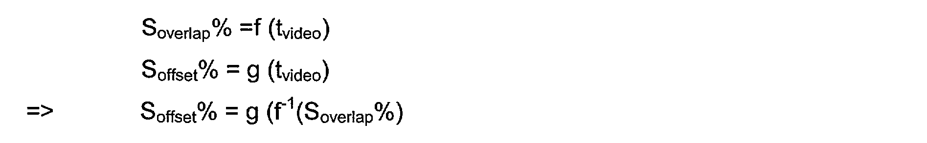
0 Soverlap ap% =f (tvideo) Soffset% = g (video) = > 0 0 = > Soffset% = g (f (Soverlap%)
Comme expliqué ci-après, les valeurs Overlap et Offset dépendent du temps de réponse du matériau cristal liquide et de la durée de la soustrame. In the embodiment of FIG. 6, the overlap data and the offset data, namely overlap and offset, are obtained from two tables LUT1 101 and LUT2 102. However, these data could be calculated one to from the other, solving for example the system of 2 equations with 2 unknowns hereafter
0 Soverlap ap% = f (tvideo) Soffset% = g (video) => 0 0 => Soffset% = g (f (Soverlap%)
As explained below, the values Overlap and Offset depend on the response time of the liquid crystal material and the duration of the subframe.
On donnera donc, avec référence à la figure 8, un exemple de réalisation des valeurs contenues dans la table LUT1 101. La figure 8 caractérise un exemple d'un matériau cristal liquide LC présentant des temps de montée et de descente linéaires pour simplifier la démonstration. With reference to FIG. 8, an exemplary embodiment of the values contained in the LUT1 table 101 will thus be given. FIG. 8 illustrates an example of a LC liquid crystal material having linear rise and fall times to simplify the demonstration. .
<Desc/Clms Page number 12> <Desc / Clms Page number 12>
La référence SOFFSET correspond à un manque de luminance dans la sous-trame bleue référence BLUE, induit par les caractéristiques de temps de montée et de descente du cristal liquide. Pour corriger cela, il est nécessaire d'ajouter un décalage de temps à la valeur bleue. Ce décalage est référencé tOFFSET'
OVERLAP correspond à la pollution de la valeur verte par la valeur bleue. Deux cas peuvent se produire comme décrits ci-avant :
La couleur de pixel n'est pas saturée. Dans ce cas, la valeur bleue n'est pas modifiée ni la valeur verte. The reference SOFFSET corresponds to a lack of luminance in the BLUE blue subframe, induced by the rise and fall time characteristics of the liquid crystal. To correct this, it is necessary to add a time offset to the blue value. This offset is referenced tOFFSET '
OVERLAP corresponds to the pollution of the green value by the blue value. Two cases may occur as described above:
The pixel color is not saturated. In this case, the blue value is not changed or the green value.
La couleur de pixel doit être saturée. Alors la valeur bleu doit être diminuée d'une valeur correspondant à SOVERLAP = valeur verte. The pixel color must be saturated. Then the blue value must be reduced by a value corresponding to SOVERLAP = green value.
En conséquence, les deux autres valeurs de couleur doivent être diminuées de la même valeur pour maintenir la teinte constante. Ceci est le rôle des fonctions de correction dans la figure 6. Si l'on calcule Soverlap et Soffset comme une fonction du signal vidéo de la sous-trame précédente Tvidéo, les temps de montée et de descente (Tr, Tf) et la période de soustrame T, le calcul conduit à :

<Desc/Clms Page number 13> <Desc / Clms Page number 13>
OVERLAP et SOFFSET sont chargés dans les tables LUT1 101 et LUT2 102. Si la vidéo est codée avec Nbit, la valeur de pourcentage doit être multipliée par 2N~1. OVERLAP and SOFFSET are loaded into the LUT1 101 and LUT2 102 tables. If the video is encoded with Nbit, the percentage value must be multiplied by 2N ~ 1.
On décrira maintenant avec référence aux figures 9 et 10, un mode de réalisation de la fonction de correction qui peut être implémentée dans les circuits 104 et 109 de la figure 6. La partie supérieure de la figure 9 représente un signal vidéo théorique présentant une première impulsion Rv de durée égale à une sous-trame, une seconde impulsion Bv très courte pendant la sous-trame suivante et une troisième impulsion Gv de durée inférieure à la durée de la troisième sous-trame. Dans ce cas, au niveau de la luminance et comme représenté sur la partie B de la figure 9, il y a une valeur overlap venant de la première sous-trame, à savoir la sous-trame RED dans le mode de réalisation représenté, sur la seconde sous-trame ou BLUE. Comme la valeur de la couleur bleue est très faible, on observe une erreur qui ne permet pas de garder la teinte. Ceci est représenté par la ligne en tireté T qui croise le front descendant de l'impulsion de luminance RED. Il en est de même pour la couleur verte. Dans ce cas, une fonction de correction doit être active pour garder la teinte. Cette fonction de correction réduit la valeur de la couleur précédente (à savoir rouge dans le mode de réalisation représenté) de telle sorte que la valeur overlap égale la valeur voulue pour la couleur bleue. Ceci est représenté sur la figure 10 sur laquelle on voit que la ligne en tireté T croise le front descendant lorsque la valeur bleue est sensiblement égale à 0. Cette fonction de correction peut être mise en oeuvre avec des additionneurs et des multiplicateurs selon la fonction de transfert ci-après en prenant comme hypothèse que les données sont codées sur 8 bits. An embodiment of the correction function which can be implemented in the circuits 104 and 109 of FIG. 6 will now be described with reference to FIGS. 9 and 10. The upper part of FIG. 9 represents a theoretical video signal presenting a first pulse Rv of duration equal to one subframe, a second pulse Bv very short during the next subframe and a third pulse Gv of duration less than the duration of the third subframe. In this case, at the luminance level and as shown in part B of FIG. 9, there is an overlap value coming from the first subframe, namely the RED subframe in the embodiment shown, on the second sub-frame or BLUE. As the value of the blue color is very low, we observe an error that does not allow to keep the hue. This is represented by the dashed line T which crosses the falling edge of the luminance pulse RED. It is the same for the green color. In this case, a correction function must be active to keep the hue. This correction function reduces the value of the previous color (ie red in the embodiment shown) so that the value overlap equals the desired value for the blue color. This is shown in FIG. 10 on which it can be seen that the dashed line T crosses the falling edge when the blue value is substantially equal to 0. This correction function can be implemented with adders and multipliers according to the function of FIG. transfer below assuming that the data is encoded on 8 bits.
Lorsque Bleue-Overlap < 0 :

<Desc/Clms Page number 14> <Desc / Clms Page number 14>
La même fonction est applicable aux autres couleurs. The same function is applicable to other colors.
Il est évident pour l'homme de l'art que les exemples ci-dessus n'ont été donnés qu'à titre illustratif. It is obvious to those skilled in the art that the above examples have been given for illustrative purposes only.
Claims (8)
Priority Applications (8)
| Application Number | Priority Date | Filing Date | Title |
|---|---|---|---|
| FR0115425A FR2832843A1 (en) | 2001-11-29 | 2001-11-29 | Method for improvement of the light yield of matrix-type displays that are controlled using pulse width modulation, such as LCOS and LCD displays, is based on adjustment of pixel time-shifts and color values |
| AU2002350704A AU2002350704A1 (en) | 2001-11-29 | 2002-11-19 | Method of improving the luminous efficiency of a sequential-colour matrix display |
| US10/496,812 US7123222B2 (en) | 2001-11-29 | 2002-11-19 | Method of improving the luminous efficiency of a sequential-color matrix display |
| JP2003548223A JP4364642B2 (en) | 2001-11-29 | 2002-11-19 | Method to improve the luminous efficiency of sequential color matrix display |
| PCT/EP2002/012941 WO2003046879A1 (en) | 2001-11-29 | 2002-11-19 | Method of improving the luminous efficiency of a sequential-colour matrix display |
| EP02785397.7A EP1449194B1 (en) | 2001-11-29 | 2002-11-19 | Method of improving the luminous efficiency of a sequential-colour matrix display |
| KR1020047007874A KR100909517B1 (en) | 2001-11-29 | 2002-11-19 | How to improve the luminous efficiency of sequential color matrix displays |
| CNB028236084A CN100347738C (en) | 2001-11-29 | 2002-11-19 | Method for Improving Luminous Efficiency of Sequential Color Matrix Display |
Applications Claiming Priority (1)
| Application Number | Priority Date | Filing Date | Title |
|---|---|---|---|
| FR0115425A FR2832843A1 (en) | 2001-11-29 | 2001-11-29 | Method for improvement of the light yield of matrix-type displays that are controlled using pulse width modulation, such as LCOS and LCD displays, is based on adjustment of pixel time-shifts and color values |
Publications (1)
| Publication Number | Publication Date |
|---|---|
| FR2832843A1 true FR2832843A1 (en) | 2003-05-30 |
Family
ID=8869905
Family Applications (1)
| Application Number | Title | Priority Date | Filing Date |
|---|---|---|---|
| FR0115425A Pending FR2832843A1 (en) | 2001-11-29 | 2001-11-29 | Method for improvement of the light yield of matrix-type displays that are controlled using pulse width modulation, such as LCOS and LCD displays, is based on adjustment of pixel time-shifts and color values |
Country Status (8)
| Country | Link |
|---|---|
| US (1) | US7123222B2 (en) |
| EP (1) | EP1449194B1 (en) |
| JP (1) | JP4364642B2 (en) |
| KR (1) | KR100909517B1 (en) |
| CN (1) | CN100347738C (en) |
| AU (1) | AU2002350704A1 (en) |
| FR (1) | FR2832843A1 (en) |
| WO (1) | WO2003046879A1 (en) |
Cited By (1)
| Publication number | Priority date | Publication date | Assignee | Title |
|---|---|---|---|---|
| WO2009089968A3 (en) * | 2008-01-16 | 2009-10-15 | Robert Bosch Gmbh | Display device for a motor vehicle, and method for representing an image |
Families Citing this family (34)
| Publication number | Priority date | Publication date | Assignee | Title |
|---|---|---|---|---|
| US7064740B2 (en) | 2001-11-09 | 2006-06-20 | Sharp Laboratories Of America, Inc. | Backlit display with improved dynamic range |
| WO2005052673A2 (en) * | 2003-11-21 | 2005-06-09 | Sharp Laboratories Of America, Inc. | Liquid crystal display with adaptive color |
| US7872631B2 (en) * | 2004-05-04 | 2011-01-18 | Sharp Laboratories Of America, Inc. | Liquid crystal display with temporal black point |
| US8395577B2 (en) * | 2004-05-04 | 2013-03-12 | Sharp Laboratories Of America, Inc. | Liquid crystal display with illumination control |
| US7602369B2 (en) | 2004-05-04 | 2009-10-13 | Sharp Laboratories Of America, Inc. | Liquid crystal display with colored backlight |
| US7612757B2 (en) * | 2004-05-04 | 2009-11-03 | Sharp Laboratories Of America, Inc. | Liquid crystal display with modulated black point |
| US7505018B2 (en) | 2004-05-04 | 2009-03-17 | Sharp Laboratories Of America, Inc. | Liquid crystal display with reduced black level insertion |
| US7532192B2 (en) | 2004-05-04 | 2009-05-12 | Sharp Laboratories Of America, Inc. | Liquid crystal display with filtered black point |
| US7777714B2 (en) * | 2004-05-04 | 2010-08-17 | Sharp Laboratories Of America, Inc. | Liquid crystal display with adaptive width |
| US7898519B2 (en) | 2005-02-17 | 2011-03-01 | Sharp Laboratories Of America, Inc. | Method for overdriving a backlit display |
| US8050512B2 (en) | 2004-11-16 | 2011-11-01 | Sharp Laboratories Of America, Inc. | High dynamic range images from low dynamic range images |
| US7525528B2 (en) | 2004-11-16 | 2009-04-28 | Sharp Laboratories Of America, Inc. | Technique that preserves specular highlights |
| US8050511B2 (en) | 2004-11-16 | 2011-11-01 | Sharp Laboratories Of America, Inc. | High dynamic range images from low dynamic range images |
| TWI288568B (en) * | 2004-12-10 | 2007-10-11 | Seiko Epson Corp | Image display method and device, and projector |
| CN101107647B (en) * | 2005-01-20 | 2010-06-02 | 皇家飞利浦电子股份有限公司 | Color sequential display device |
| US7701451B1 (en) * | 2005-07-29 | 2010-04-20 | Pixelworks, Inc. | Boost look up table compression system and method |
| US20070030294A1 (en) * | 2005-08-05 | 2007-02-08 | Texas Instruments Incorporated | System and method for implementation of transition zone associated with an actuator for an optical device in a display system |
| US8121401B2 (en) | 2006-01-24 | 2012-02-21 | Sharp Labortories of America, Inc. | Method for reducing enhancement of artifacts and noise in image color enhancement |
| US9143657B2 (en) | 2006-01-24 | 2015-09-22 | Sharp Laboratories Of America, Inc. | Color enhancement technique using skin color detection |
| US8111271B2 (en) * | 2006-04-27 | 2012-02-07 | Jasper Display Corporation | Gray scale drive sequences for pulse width modulated displays |
| US7852307B2 (en) * | 2006-04-28 | 2010-12-14 | Jasper Display Corp. | Multi-mode pulse width modulated displays |
| US8941580B2 (en) | 2006-11-30 | 2015-01-27 | Sharp Laboratories Of America, Inc. | Liquid crystal display with area adaptive backlight |
| CN101308631B (en) * | 2007-05-14 | 2012-03-21 | 奇美电子股份有限公司 | Driving unit with timing controller and driving method thereof |
| US9767757B2 (en) | 2013-01-24 | 2017-09-19 | Finisar Corporation | Pipelined pixel applications in liquid crystal on silicon chip |
| US11030942B2 (en) | 2017-10-13 | 2021-06-08 | Jasper Display Corporation | Backplane adaptable to drive emissive pixel arrays of differing pitches |
| US10951875B2 (en) | 2018-07-03 | 2021-03-16 | Raxium, Inc. | Display processing circuitry |
| US11710445B2 (en) | 2019-01-24 | 2023-07-25 | Google Llc | Backplane configurations and operations |
| US11637219B2 (en) | 2019-04-12 | 2023-04-25 | Google Llc | Monolithic integration of different light emitting structures on a same substrate |
| US11238782B2 (en) | 2019-06-28 | 2022-02-01 | Jasper Display Corp. | Backplane for an array of emissive elements |
| US11626062B2 (en) | 2020-02-18 | 2023-04-11 | Google Llc | System and method for modulating an array of emissive elements |
| WO2021207129A1 (en) | 2020-04-06 | 2021-10-14 | Raxium, Inc. | Display assemblies |
| US11538431B2 (en) | 2020-06-29 | 2022-12-27 | Google Llc | Larger backplane suitable for high speed applications |
| CN116601547A (en) | 2020-12-21 | 2023-08-15 | 谷歌有限责任公司 | High-density pixel arrays for free-viewing 3D displays |
| US11810509B2 (en) | 2021-07-14 | 2023-11-07 | Google Llc | Backplane and method for pulse width modulation |
Citations (3)
| Publication number | Priority date | Publication date | Assignee | Title |
|---|---|---|---|---|
| US4907862A (en) * | 1985-03-05 | 1990-03-13 | Oy Lohja Ab | Method for generating elecronically controllable color elements and color display based on the method |
| US5461397A (en) * | 1992-10-08 | 1995-10-24 | Panocorp Display Systems | Display device with a light shutter front end unit and gas discharge back end unit |
| US5767828A (en) * | 1995-07-20 | 1998-06-16 | The Regents Of The University Of Colorado | Method and apparatus for displaying grey-scale or color images from binary images |
Family Cites Families (5)
| Publication number | Priority date | Publication date | Assignee | Title |
|---|---|---|---|---|
| CN1089040A (en) * | 1992-10-08 | 1994-07-06 | 潘诺科普显示系统公司 | The display device of forming by preposition unit of grating and gas discharge back unit |
| JP3617206B2 (en) * | 1996-08-16 | 2005-02-02 | セイコーエプソン株式会社 | Display device, electronic apparatus, and driving method |
| JPH1063225A (en) * | 1996-08-19 | 1998-03-06 | Citizen Watch Co Ltd | Display device |
| US5977942A (en) | 1996-12-20 | 1999-11-02 | Compaq Computer Corporation | Multiplexed display element sequential color LCD panel |
| US6573951B1 (en) * | 1998-10-09 | 2003-06-03 | Texas Instruments Incorporated | Non-terminating pulse width modulation for displays |
-
2001
- 2001-11-29 FR FR0115425A patent/FR2832843A1/en active Pending
-
2002
- 2002-11-19 JP JP2003548223A patent/JP4364642B2/en not_active Expired - Fee Related
- 2002-11-19 CN CNB028236084A patent/CN100347738C/en not_active Expired - Fee Related
- 2002-11-19 KR KR1020047007874A patent/KR100909517B1/en not_active Expired - Fee Related
- 2002-11-19 WO PCT/EP2002/012941 patent/WO2003046879A1/en not_active Ceased
- 2002-11-19 EP EP02785397.7A patent/EP1449194B1/en not_active Expired - Lifetime
- 2002-11-19 AU AU2002350704A patent/AU2002350704A1/en not_active Abandoned
- 2002-11-19 US US10/496,812 patent/US7123222B2/en not_active Expired - Lifetime
Patent Citations (3)
| Publication number | Priority date | Publication date | Assignee | Title |
|---|---|---|---|---|
| US4907862A (en) * | 1985-03-05 | 1990-03-13 | Oy Lohja Ab | Method for generating elecronically controllable color elements and color display based on the method |
| US5461397A (en) * | 1992-10-08 | 1995-10-24 | Panocorp Display Systems | Display device with a light shutter front end unit and gas discharge back end unit |
| US5767828A (en) * | 1995-07-20 | 1998-06-16 | The Regents Of The University Of Colorado | Method and apparatus for displaying grey-scale or color images from binary images |
Cited By (1)
| Publication number | Priority date | Publication date | Assignee | Title |
|---|---|---|---|---|
| WO2009089968A3 (en) * | 2008-01-16 | 2009-10-15 | Robert Bosch Gmbh | Display device for a motor vehicle, and method for representing an image |
Also Published As
| Publication number | Publication date |
|---|---|
| KR20040064284A (en) | 2004-07-16 |
| US20050088462A1 (en) | 2005-04-28 |
| KR100909517B1 (en) | 2009-07-27 |
| CN100347738C (en) | 2007-11-07 |
| AU2002350704A1 (en) | 2003-06-10 |
| WO2003046879A1 (en) | 2003-06-05 |
| EP1449194B1 (en) | 2016-05-25 |
| JP4364642B2 (en) | 2009-11-18 |
| EP1449194A1 (en) | 2004-08-25 |
| US7123222B2 (en) | 2006-10-17 |
| CN1596431A (en) | 2005-03-16 |
| JP2005510770A (en) | 2005-04-21 |
Similar Documents
| Publication | Publication Date | Title |
|---|---|---|
| FR2832843A1 (en) | Method for improvement of the light yield of matrix-type displays that are controlled using pulse width modulation, such as LCOS and LCD displays, is based on adjustment of pixel time-shifts and color values | |
| FR2862420A1 (en) | METHOD AND DEVICE FOR CONTROLLING A LIQUID CRYSTAL DISPLAY | |
| FR2805380A1 (en) | APPARATUS FOR CONTROLLING A PLASMA DISPLAY PANEL AND CONTROL METHOD | |
| FR2857147A1 (en) | METHOD FOR PROCESSING A SEQUENCE OF VIDEO IMAGES IN A LIQUID CRYSTAL DISPLAY PANEL | |
| EP3079142B1 (en) | Method for displaying images on a matrix screen | |
| FR2880460A1 (en) | METHOD AND DISPLAY DEVICE FOR REDUCING THE EFFECTS OF FLOU | |
| FR2890776A1 (en) | DISPLAY DEVICE AND METHOD FOR CONTROLLING THE SAME | |
| EP0641475B1 (en) | Method for displaying different levels of gray and system for implementing such method | |
| FR2884640A1 (en) | METHOD FOR DISPLAYING A VIDEO IMAGE AND DISPLAY PANEL USING THE METHOD | |
| FR2656757A1 (en) | METHOD FOR ADDRESSING EACH COLUMN OF A MATRIX TYPE LCD SCREEN. | |
| FR2708371A1 (en) | High persistence display circuit and associated method. | |
| EP2022037B1 (en) | Methods for sequential color display by modulation of pulses | |
| EP0774746A1 (en) | Control method for a panel display and display device for carrying out the method | |
| EP1958182B1 (en) | Video system including a liquid crystal matrix display with improved addressing method | |
| FR2903203A1 (en) | LIQUID CRYSTAL DISPLAY DEVICE | |
| EP1774505B1 (en) | Liquid-crystal matrix display | |
| EP0907945B1 (en) | Method for activating the cells of an image displaying screen, and image displaying device using same | |
| EP1958183B1 (en) | Colour sequential liquid crystal matrix display | |
| FR2698202A1 (en) | Electronic display screen control circuit for e.g. liquid crystal display - uses sample=hold circuits and multiplexer to control individual rows and columns of liquid crystal display | |
| FR2889763A1 (en) | MATRIX DISPLAY WITH SEQUENTIAL COLOR DISPLAY AND ADDRESSING METHOD | |
| EP1964094A1 (en) | Method for controlling a display panel by capacitive coupling | |
| EP0793212B1 (en) | Control method for a display screen with gradation display and display device for carrying out the same | |
| CA2536216A1 (en) | Liquid crystal microdisplay and control method thereof | |
| EP0793213A1 (en) | Driving method for an image display screen using the principle of modulation of the light emission duration, and display device using this method | |
| FR2866465A1 (en) | Front/rear projector type image display device stores specific and common values associated with video data to be displayed by each liquid crystal element of valve and group of at least two adjacent elements respectively |