FR2832542A1 - MAGNETIC DEVICE WITH MAGNETIC TUNNEL JUNCTION, MEMORY AND WRITING AND READING METHODS USING THE SAME - Google Patents
MAGNETIC DEVICE WITH MAGNETIC TUNNEL JUNCTION, MEMORY AND WRITING AND READING METHODS USING THE SAME Download PDFInfo
- Publication number
- FR2832542A1 FR2832542A1 FR0114840A FR0114840A FR2832542A1 FR 2832542 A1 FR2832542 A1 FR 2832542A1 FR 0114840 A FR0114840 A FR 0114840A FR 0114840 A FR0114840 A FR 0114840A FR 2832542 A1 FR2832542 A1 FR 2832542A1
- Authority
- FR
- France
- Prior art keywords
- layer
- magnetization
- magnetic
- storage layer
- layers
- Prior art date
- Legal status (The legal status is an assumption and is not a legal conclusion. Google has not performed a legal analysis and makes no representation as to the accuracy of the status listed.)
- Granted
Links
- 230000005291 magnetic effect Effects 0.000 title claims abstract description 148
- 230000015654 memory Effects 0.000 title claims abstract description 68
- 238000000034 method Methods 0.000 title claims abstract description 18
- 238000003860 storage Methods 0.000 claims abstract description 133
- 230000005415 magnetization Effects 0.000 claims abstract description 122
- 230000000903 blocking effect Effects 0.000 claims abstract description 51
- 238000010438 heat treatment Methods 0.000 claims abstract description 23
- 239000010410 layer Substances 0.000 claims description 332
- 230000005290 antiferromagnetic effect Effects 0.000 claims description 33
- BASFCYQUMIYNBI-UHFFFAOYSA-N platinum Substances [Pt] BASFCYQUMIYNBI-UHFFFAOYSA-N 0.000 claims description 25
- 238000001816 cooling Methods 0.000 claims description 23
- 229910045601 alloy Inorganic materials 0.000 claims description 13
- 239000000956 alloy Substances 0.000 claims description 13
- PXHVJJICTQNCMI-UHFFFAOYSA-N Nickel Chemical compound [Ni] PXHVJJICTQNCMI-UHFFFAOYSA-N 0.000 claims description 12
- 230000007423 decrease Effects 0.000 claims description 12
- XEEYBQQBJWHFJM-UHFFFAOYSA-N Iron Chemical compound [Fe] XEEYBQQBJWHFJM-UHFFFAOYSA-N 0.000 claims description 10
- 229910052697 platinum Inorganic materials 0.000 claims description 10
- KDLHZDBZIXYQEI-UHFFFAOYSA-N palladium Substances [Pd] KDLHZDBZIXYQEI-UHFFFAOYSA-N 0.000 claims description 9
- 229910017052 cobalt Inorganic materials 0.000 claims description 7
- 239000010941 cobalt Substances 0.000 claims description 7
- GUTLYIVDDKVIGB-UHFFFAOYSA-N cobalt atom Chemical compound [Co] GUTLYIVDDKVIGB-UHFFFAOYSA-N 0.000 claims description 7
- 229910052759 nickel Inorganic materials 0.000 claims description 7
- 229910052763 palladium Inorganic materials 0.000 claims description 7
- 229910052742 iron Inorganic materials 0.000 claims description 6
- 229910052804 chromium Inorganic materials 0.000 claims description 5
- 239000011651 chromium Substances 0.000 claims description 5
- VYZAMTAEIAYCRO-UHFFFAOYSA-N Chromium Chemical compound [Cr] VYZAMTAEIAYCRO-UHFFFAOYSA-N 0.000 claims description 4
- 230000003993 interaction Effects 0.000 claims description 4
- 239000011159 matrix material Substances 0.000 claims description 4
- 239000002356 single layer Substances 0.000 claims description 4
- 229910020708 Co—Pd Inorganic materials 0.000 claims description 2
- 229910020707 Co—Pt Inorganic materials 0.000 claims description 2
- 229910052741 iridium Inorganic materials 0.000 claims description 2
- 229910052702 rhenium Inorganic materials 0.000 claims description 2
- 229910052707 ruthenium Inorganic materials 0.000 claims description 2
- 229910052703 rhodium Inorganic materials 0.000 claims 1
- 239000004065 semiconductor Substances 0.000 abstract description 3
- 239000000463 material Substances 0.000 description 25
- 230000004888 barrier function Effects 0.000 description 11
- 230000000694 effects Effects 0.000 description 8
- 230000006870 function Effects 0.000 description 8
- 229910005335 FePt Inorganic materials 0.000 description 7
- 229910019041 PtMn Inorganic materials 0.000 description 7
- 230000008901 benefit Effects 0.000 description 6
- 239000004020 conductor Substances 0.000 description 6
- 230000008878 coupling Effects 0.000 description 6
- 238000010168 coupling process Methods 0.000 description 6
- 238000005859 coupling reaction Methods 0.000 description 6
- 238000002347 injection Methods 0.000 description 6
- 239000007924 injection Substances 0.000 description 6
- 239000002885 antiferromagnetic material Substances 0.000 description 4
- 229920006395 saturated elastomer Polymers 0.000 description 4
- PNEYBMLMFCGWSK-UHFFFAOYSA-N aluminium oxide Inorganic materials [O-2].[O-2].[O-2].[Al+3].[Al+3] PNEYBMLMFCGWSK-UHFFFAOYSA-N 0.000 description 3
- 238000009826 distribution Methods 0.000 description 3
- 230000010354 integration Effects 0.000 description 3
- 229910052802 copper Inorganic materials 0.000 description 2
- 239000010949 copper Substances 0.000 description 2
- 230000005294 ferromagnetic effect Effects 0.000 description 2
- 239000000696 magnetic material Substances 0.000 description 2
- 238000004519 manufacturing process Methods 0.000 description 2
- 230000007246 mechanism Effects 0.000 description 2
- 230000010287 polarization Effects 0.000 description 2
- 101100450272 Caenorhabditis elegans hcf-1 gene Proteins 0.000 description 1
- 229910018979 CoPt Inorganic materials 0.000 description 1
- RYGMFSIKBFXOCR-UHFFFAOYSA-N Copper Chemical compound [Cu] RYGMFSIKBFXOCR-UHFFFAOYSA-N 0.000 description 1
- 229910015136 FeMn Inorganic materials 0.000 description 1
- 229910015187 FePd Inorganic materials 0.000 description 1
- 229910003289 NiMn Inorganic materials 0.000 description 1
- 238000009825 accumulation Methods 0.000 description 1
- 238000003491 array Methods 0.000 description 1
- 230000002457 bidirectional effect Effects 0.000 description 1
- 230000003247 decreasing effect Effects 0.000 description 1
- 230000001419 dependent effect Effects 0.000 description 1
- 238000005265 energy consumption Methods 0.000 description 1
- 238000005530 etching Methods 0.000 description 1
- 238000001459 lithography Methods 0.000 description 1
- 230000008569 process Effects 0.000 description 1
- 230000001902 propagating effect Effects 0.000 description 1
- 230000009467 reduction Effects 0.000 description 1
- 230000007306 turnover Effects 0.000 description 1
- 229910052720 vanadium Inorganic materials 0.000 description 1
Classifications
-
- H—ELECTRICITY
- H01—ELECTRIC ELEMENTS
- H01F—MAGNETS; INDUCTANCES; TRANSFORMERS; SELECTION OF MATERIALS FOR THEIR MAGNETIC PROPERTIES
- H01F10/00—Thin magnetic films, e.g. of one-domain structure
- H01F10/32—Spin-exchange-coupled multilayers, e.g. nanostructured superlattices
- H01F10/324—Exchange coupling of magnetic film pairs via a very thin non-magnetic spacer, e.g. by exchange with conduction electrons of the spacer
- H01F10/3254—Exchange coupling of magnetic film pairs via a very thin non-magnetic spacer, e.g. by exchange with conduction electrons of the spacer the spacer being semiconducting or insulating, e.g. for spin tunnel junction [STJ]
-
- B—PERFORMING OPERATIONS; TRANSPORTING
- B82—NANOTECHNOLOGY
- B82Y—SPECIFIC USES OR APPLICATIONS OF NANOSTRUCTURES; MEASUREMENT OR ANALYSIS OF NANOSTRUCTURES; MANUFACTURE OR TREATMENT OF NANOSTRUCTURES
- B82Y25/00—Nanomagnetism, e.g. magnetoimpedance, anisotropic magnetoresistance, giant magnetoresistance or tunneling magnetoresistance
-
- G—PHYSICS
- G11—INFORMATION STORAGE
- G11C—STATIC STORES
- G11C11/00—Digital stores characterised by the use of particular electric or magnetic storage elements; Storage elements therefor
- G11C11/02—Digital stores characterised by the use of particular electric or magnetic storage elements; Storage elements therefor using magnetic elements
- G11C11/16—Digital stores characterised by the use of particular electric or magnetic storage elements; Storage elements therefor using magnetic elements using elements in which the storage effect is based on magnetic spin effect
- G11C11/161—Digital stores characterised by the use of particular electric or magnetic storage elements; Storage elements therefor using magnetic elements using elements in which the storage effect is based on magnetic spin effect details concerning the memory cell structure, e.g. the layers of the ferromagnetic memory cell
-
- G—PHYSICS
- G11—INFORMATION STORAGE
- G11C—STATIC STORES
- G11C11/00—Digital stores characterised by the use of particular electric or magnetic storage elements; Storage elements therefor
- G11C11/02—Digital stores characterised by the use of particular electric or magnetic storage elements; Storage elements therefor using magnetic elements
- G11C11/16—Digital stores characterised by the use of particular electric or magnetic storage elements; Storage elements therefor using magnetic elements using elements in which the storage effect is based on magnetic spin effect
- G11C11/165—Auxiliary circuits
- G11C11/1659—Cell access
-
- G—PHYSICS
- G11—INFORMATION STORAGE
- G11C—STATIC STORES
- G11C11/00—Digital stores characterised by the use of particular electric or magnetic storage elements; Storage elements therefor
- G11C11/02—Digital stores characterised by the use of particular electric or magnetic storage elements; Storage elements therefor using magnetic elements
- G11C11/16—Digital stores characterised by the use of particular electric or magnetic storage elements; Storage elements therefor using magnetic elements using elements in which the storage effect is based on magnetic spin effect
- G11C11/165—Auxiliary circuits
- G11C11/1675—Writing or programming circuits or methods
-
- G—PHYSICS
- G11—INFORMATION STORAGE
- G11C—STATIC STORES
- G11C11/00—Digital stores characterised by the use of particular electric or magnetic storage elements; Storage elements therefor
- G11C11/56—Digital stores characterised by the use of particular electric or magnetic storage elements; Storage elements therefor using storage elements with more than two stable states represented by steps, e.g. of voltage, current, phase, frequency
- G11C11/5607—Digital stores characterised by the use of particular electric or magnetic storage elements; Storage elements therefor using storage elements with more than two stable states represented by steps, e.g. of voltage, current, phase, frequency using magnetic storage elements
-
- H—ELECTRICITY
- H01—ELECTRIC ELEMENTS
- H01F—MAGNETS; INDUCTANCES; TRANSFORMERS; SELECTION OF MATERIALS FOR THEIR MAGNETIC PROPERTIES
- H01F10/00—Thin magnetic films, e.g. of one-domain structure
- H01F10/32—Spin-exchange-coupled multilayers, e.g. nanostructured superlattices
- H01F10/324—Exchange coupling of magnetic film pairs via a very thin non-magnetic spacer, e.g. by exchange with conduction electrons of the spacer
- H01F10/3286—Spin-exchange coupled multilayers having at least one layer with perpendicular magnetic anisotropy
-
- H—ELECTRICITY
- H01—ELECTRIC ELEMENTS
- H01F—MAGNETS; INDUCTANCES; TRANSFORMERS; SELECTION OF MATERIALS FOR THEIR MAGNETIC PROPERTIES
- H01F10/00—Thin magnetic films, e.g. of one-domain structure
- H01F10/32—Spin-exchange-coupled multilayers, e.g. nanostructured superlattices
- H01F10/324—Exchange coupling of magnetic film pairs via a very thin non-magnetic spacer, e.g. by exchange with conduction electrons of the spacer
- H01F10/329—Spin-exchange coupled multilayers wherein the magnetisation of the free layer is switched by a spin-polarised current, e.g. spin torque effect
-
- H—ELECTRICITY
- H10—SEMICONDUCTOR DEVICES; ELECTRIC SOLID-STATE DEVICES NOT OTHERWISE PROVIDED FOR
- H10B—ELECTRONIC MEMORY DEVICES
- H10B61/00—Magnetic memory devices, e.g. magnetoresistive RAM [MRAM] devices
- H10B61/20—Magnetic memory devices, e.g. magnetoresistive RAM [MRAM] devices comprising components having three or more electrodes, e.g. transistors
- H10B61/22—Magnetic memory devices, e.g. magnetoresistive RAM [MRAM] devices comprising components having three or more electrodes, e.g. transistors of the field-effect transistor [FET] type
-
- H—ELECTRICITY
- H10—SEMICONDUCTOR DEVICES; ELECTRIC SOLID-STATE DEVICES NOT OTHERWISE PROVIDED FOR
- H10N—ELECTRIC SOLID-STATE DEVICES NOT OTHERWISE PROVIDED FOR
- H10N50/00—Galvanomagnetic devices
- H10N50/10—Magnetoresistive devices
-
- H—ELECTRICITY
- H01—ELECTRIC ELEMENTS
- H01F—MAGNETS; INDUCTANCES; TRANSFORMERS; SELECTION OF MATERIALS FOR THEIR MAGNETIC PROPERTIES
- H01F10/00—Thin magnetic films, e.g. of one-domain structure
- H01F10/32—Spin-exchange-coupled multilayers, e.g. nanostructured superlattices
- H01F10/324—Exchange coupling of magnetic film pairs via a very thin non-magnetic spacer, e.g. by exchange with conduction electrons of the spacer
- H01F10/3268—Exchange coupling of magnetic film pairs via a very thin non-magnetic spacer, e.g. by exchange with conduction electrons of the spacer the exchange coupling being asymmetric, e.g. by use of additional pinning, by using antiferromagnetic or ferromagnetic coupling interface, i.e. so-called spin-valve [SV] structure, e.g. NiFe/Cu/NiFe/FeMn
- H01F10/3272—Exchange coupling of magnetic film pairs via a very thin non-magnetic spacer, e.g. by exchange with conduction electrons of the spacer the exchange coupling being asymmetric, e.g. by use of additional pinning, by using antiferromagnetic or ferromagnetic coupling interface, i.e. so-called spin-valve [SV] structure, e.g. NiFe/Cu/NiFe/FeMn by use of anti-parallel coupled [APC] ferromagnetic layers, e.g. artificial ferrimagnets [AFI], artificial [AAF] or synthetic [SAF] anti-ferromagnets
Landscapes
- Engineering & Computer Science (AREA)
- Chemical & Material Sciences (AREA)
- Crystallography & Structural Chemistry (AREA)
- Computer Hardware Design (AREA)
- Power Engineering (AREA)
- Nanotechnology (AREA)
- Mram Or Spin Memory Techniques (AREA)
- Hall/Mr Elements (AREA)
- Semiconductor Memories (AREA)
- Thin Magnetic Films (AREA)
Abstract
Description
<Desc/Clms Page number 1> <Desc / Clms Page number 1>
DISPOSITIF MAGNETIQUE A JONCTION TUNNEL MAGNETIQUE, MEMOIRE ET PROCEDES D'ECRITURE ET DE LECTURE UTILISANT
CE DISPOSITIF
DESCRIPTION DOMAINE TECHNIQUE
La présente invention concerne un dispositif magnétique à jonction tunnel ainsi qu'une mémoire utilisant ce dispositif. MAGNETIC DEVICE WITH MAGNETIC TUNNEL JUNCTION, MEMORY AND METHODS OF WRITING AND READING USING
THESE MEASURES
DESCRIPTION TECHNICAL FIELD
The present invention relates to a magnetic device with tunnel junction and a memory using this device.
L'invention concerne aussi un procédé d'écriture thermomagnétique dans ce dispositif ainsi qu'un procédé de lecture du dispositif. The invention also relates to a thermomagnetic writing method in this device as well as to a device reading method.
L'invention trouve une application en électronique et notamment dans la réalisation de points mémoires et de mémoires de type MRAM ("Magnetic Random Access Memory"ou mémoire magnétique à accès direct (ou aléatoire)). The invention finds an application in electronics and in particular in the production of memory points and memories of the MRAM type ("Magnetic Random Access Memory" or magnetic memory with direct (or random) access).
ETAT DE LA TECHNIQUE ANTÉRIEURE
Les mémoires magnétiques MRAM ont connu un regain d'intérêt avec la mise au point de jonctions tunnel magnétiques (en abrégé MTJ pour"Magnetic Tunnel Junction") présentant une forte magnétorésistance à température ambiante. PRIOR STATE OF THE ART
MRAM magnetic memories have seen a renewed interest with the development of magnetic tunnel junctions (abbreviated as MTJ for "Magnetic Tunnel Junction") having a strong magnetoresistance at room temperature.
Au sujet des mémoires magnétiques utilisant des jonctions tunnel magnétiques, on consultera par exemple les documents suivants : [1] US 5 640 343 A (Gallagher et al.) [2] S. S. P. Parkin et al., J. Appl. Phys., vol. 85 n08, 1999, pp. 5828-5833. With regard to magnetic memories using magnetic tunnel junctions, the following documents are for example: [1] US 5,640,343 A (Gallagher et al.) [2] S.S.P. Parkin et al., J. Appl. Phys., Vol. 85 n08, 1999, pp. 5828-5833.
<Desc/Clms Page number 2> <Desc / Clms Page number 2>
Les figures 1A et 1B annexées illustrent schématiquement la structure et la fonction d'une jonction tunnel magnétique connue. FIGS. 1A and 1B annexed schematically illustrate the structure and the function of a known magnetic tunnel junction.
La jonction porte la référence 2. Il s'agit d'un empilement comprenant une couche d'oxyde 3b en sandwich entre deux couches magnétiques. Ce système fonctionne comme une vanne de spin, à la différence que le courant circule perpendiculairement aux plans des couches. The junction bears the reference 2. It is a stack comprising an oxide layer 3b sandwiched between two magnetic layers. This system functions as a spin valve, with the difference that the current flows perpendicular to the plane of the layers.
L'une 3a des couches magnétiques est dite "libre"ou"de stockage"car on peut orienter son aimantation dans la direction désirée à l'aide d'un champ magnétique extérieur (flèche bidirectionnelle) ; l'autre couche magnétique 3c est dite "piégée" ou "de référence'car sa direction d'aimantation est fixée par couplage d'échange avec une couche antiferromagnétique (flèche unidirectionnelle). One of the magnetic layers 3a is said to be "free" or "storage" because its magnetization can be oriented in the desired direction by means of an external magnetic field (bidirectional arrow); the other magnetic layer 3c is said to be "trapped" or "referenced" because its direction of magnetization is fixed by exchange coupling with an antiferromagnetic layer (unidirectional arrow).
Lorsque les aimantations des couches magnétiques sont antiparallèles, la résistance de la jonction est élevée ; lorsque les aimantations sont parallèles, cette résistance devient faible. La variation relative de résistance entre ces deux états peut atteindre 40% par un choix approprié des matériaux des couches de l'empilement et/ou de traitements thermiques de ces matériaux. When the magnetizations of the magnetic layers are antiparallel, the strength of the junction is high; when the magnetizations are parallel, this resistance becomes weak. The relative variation in resistance between these two states can reach 40% by appropriate choice of materials of the layers of the stack and / or heat treatments of these materials.
La jonction 2 est placée entre un transistor de commutation 4 et une ligne d'amenée de courant 6 formant une ligne conductrice supérieure. Un courant Il passant dans celle-ci produit un premier champ magnétique 7. Un conducteur 8 formant une ligne conductrice inférieure, orthogonale à la ligne d'amenée The junction 2 is placed between a switching transistor 4 and a current supply line 6 forming an upper conductive line. A current flowing in it produces a first magnetic field 7. A conductor 8 forming a lower conductive line, orthogonal to the supply line
<Desc/Clms Page number 3><Desc / Clms Page number 3>
de courant 6 permet, en y faisant circuler un courant 12, de produire un second champ magnétique 9. of current 6 makes it possible, by circulating a current 12, to produce a second magnetic field 9.
Dans le mode"écriture" (figure lA), le transistor 4 est placé en mode bloqué et aucun courant ne traverse donc ce transistor. On fait circuler des impulsions de courant dans la ligne d'amenée de courant 6 et dans le conducteur 8. La jonction 2 est donc soumise à deux champs magnétiques orthogonaux. L'un est appliqué selon l'axe de difficile aimantation de la couche libre 3a, afin de réduire son champ de retournement, tandis que l'autre et appliqué selon son axe facile afin de provoquer le retournement de l'aimantation et donc l'écriture du point mémoire. In the "write" mode (FIG. 1A), the transistor 4 is placed in the blocked mode and no current therefore flows through this transistor. Current pulses are circulated in the current supply line 6 and in the conductor 8. The junction 2 is therefore subjected to two orthogonal magnetic fields. One is applied along the axis of difficult magnetization of the free layer 3a, in order to reduce its reversal field, while the other is applied along its easy axis in order to cause the reversal of the magnetization and therefore the writing of the memory point.
Dans le principe, seul le point mémoire placé à l'intersection des deux lignes 6 et 8 est susceptible de se retourner, car chaque champ magnétique pris individuellement n'est pas suffisamment grand pour provoquer un basculement de l'aimantation. In principle, only the memory point placed at the intersection of the two lines 6 and 8 is likely to turn over, because each magnetic field taken individually is not large enough to cause a tilting of the magnetization.
Dans le mode"lecture" (figure 1B), le transistor est placé en régime saturé (c'est-à-dire que le courant traversant ce transistor est maximum) par l'envoi d'une impulsion de courant positive dans la grille du transistor. Le courant 13 envoyé dans la ligne 6 traverse uniquement le point mémoire dont le transistor est placé en mode saturé. In the "read" mode (FIG. 1B), the transistor is placed in a saturated state (that is to say that the current flowing through this transistor is maximum) by sending a positive current pulse into the gate of the transistor. transistor. The current 13 sent in the line 6 passes only the memory point whose transistor is placed in saturated mode.
Ce courant permet de mesurer la résistance de la jonction de ce point mémoire. Par comparaison avec un point mémoire de référence, l'état du point mémoire ("O"ou"l") peut ainsi être déterminé : on sait alors si l'aimantation de la couche de stockage 3a est parallèle au antiparallèle à celle de la couche de This current makes it possible to measure the resistance of the junction of this memory point. By comparison with a reference memory point, the state of the memory point ("O" or "l") can thus be determined: it is then known whether the magnetization of the storage layer 3a is parallel to the antiparallel to that of the layer of
<Desc/Clms Page number 4><Desc / Clms Page number 4>
référence 3c. reference 3c.
Un tel mécanisme d'écriture présente des inconvénients en particulier dans un réseau de jonctions tunnel :
1) Comme le renversement de l'aimantation de la couche libre d'une jonction se produit sous l'effet de champs extérieurs et comme les champs de retournement sont statistiquement distribués, il n'est pas impossible de retourner accidentellement certaines jonctions voisines simplement par l'effet du champ magnétique produit le long d'une ligne conductrice inférieure ou supérieure. Comme, pour des mémoires à haute densité, la taille des points mémoires est nettement submicronique, le nombre d'erreurs d'adressage augmente. Such a writing mechanism has drawbacks in particular in a network of tunnel junctions:
1) As the reversal of the magnetization of the free layer of a junction occurs under the effect of external fields and as the turning fields are statistically distributed, it is not impossible to accidentally return some neighboring junctions simply by the effect of the magnetic field produced along a lower or higher conductive line. Since, for high density memories, the size of the memory points is substantially submicron, the number of addressing errors increases.
2) La diminution de la taille des points mémoires entraîne une augmentation de la valeur du champ de retournement individuel ; un courant plus important est alors nécessaire pour écrire les points mémoires, ce qui tend à augmenter la consommation électrique. 2) The decrease in the size of the memory points results in an increase in the value of the individual reversal field; a larger current is then required to write the memory points, which tends to increase the power consumption.
3) Le mode d'écriture utilise deux lignes de courant à 900, ce qui limite la densité d'intégration. 3) The writing mode uses two current lines at 900, which limits the integration density.
EXPOSE DE L'INVENTION
La présente invention a pour but de remédier aux inconvénients précédents. STATEMENT OF THE INVENTION
The present invention aims to remedy the above drawbacks.
Selon un aspect de la présente invention, on propose un dispositif magnétique à jonction tunnel magnétique qui est utilisable dans une MRAM et dans lequel le mécanisme d'écriture est insensible à la According to one aspect of the present invention there is provided a magnetic tunnel junction magnetic device which is usable in an MRAM and in which the writing mechanism is insensitive to the
<Desc/Clms Page number 5><Desc / Clms Page number 5>
distribution des champs de retournement pour éliminer les erreurs d'adressage et obtenir une bonne reproductibilité de l'écriture des informations. distribution of the fields of rotation to eliminate the errors of addressing and to obtain a good reproducibility of the writing of the information.
Selon un autre aspect de l'invention, on propose un dispositif magnétique à jonction tunnel magnétique dont la consommation en énergie est faible. According to another aspect of the invention, there is provided a magnetic magnetic junction magnetic device whose energy consumption is low.
Selon encore un autre aspect, on propose un dispositif magnétique à jonction tunnel magnétique permettant un stockage multi-niveaux d'informations. According to yet another aspect, a magnetic device with a magnetic tunnel junction is proposed allowing multi-level storage of information.
Cela présente l'avantage, dans une mémoire conforme à l'invention, d'accroître la capacité de stockage pour un même nombre de points mémoires. This has the advantage, in a memory according to the invention, of increasing the storage capacity for the same number of memory points.
La présente invention a également pour but d'améliorer les mémoires magnétiques en diminuant la taille de leurs points mémoires, tout en gardant l'information stable à température ambiante, ainsi que le taux d'erreur d'écriture de ces mémoires. The present invention also aims to improve the magnetic memories by decreasing the size of their memory points, while keeping the information stable at room temperature, as well as the write error rate of these memories.
Dans l'invention, on utilise une propriété connue d'un matériau magnétique, selon laquelle le champ de retournement de l'aimantation est très faible lorsqu'on élève la température de ce matériau au-delà de la température de blocage de l'aimantation de ce matériau. In the invention, a known property of a magnetic material is used, according to which the reversal field of the magnetization is very low when the temperature of this material is raised above the magnetization blocking temperature. of this material.
De façon précise, la présente invention a pour objet un dispositif magnétique comprenant une jonction tunnel magnétique qui comporte : - une première couche magnétique formant une couche de référence et ayant une aimantation de direction fixe, - une deuxième couche magnétique formant une couche de stockage et ayant une aimantation de Specifically, the present invention relates to a magnetic device comprising a magnetic tunnel junction which comprises: - a first magnetic layer forming a reference layer and having a magnetization of fixed direction, - a second magnetic layer forming a storage layer and having a magnetization of
<Desc/Clms Page number 6><Desc / Clms Page number 6>
direction variable, et - une troisième couche qui est semiconductrice ou électriquement isolante et qui sépare la première couche de la deuxième couche, ce dispositif étant caractérisé en ce que la température de blocage de l'aimantation de la couche de stockage est inférieure à la température de blocage de l'aimantation de la couche de référence et en ce que le dispositif comprend en outre : - des moyens d'échauffement de la couche de stockage à une température supérieure à la température de blocage de l'aimantation de cette couche de stockage et - des moyens d'application, à cette couche de stockage, d'un champ magnétique apte à orienter l'aimantation de cette couche de stockage par rapport à l'aimantation de la couche référence, sans modifier l'orientation de cette couche de référence. variable direction, and - a third layer which is semiconductor or electrically insulating and which separates the first layer from the second layer, this device being characterized in that the blocking temperature of the magnetization of the storage layer is lower than the temperature for blocking the magnetization of the reference layer and in that the device further comprises: - means for heating the storage layer to a temperature higher than the temperature for blocking the magnetization of this storage layer and - means for applying, to this storage layer, a magnetic field capable of orienting the magnetization of this storage layer relative to the magnetization of the reference layer, without modifying the orientation of this layer of reference.
Selon un mode de réalisation préféré de l'invention, les températures de blocage des couches de stockage et de référence ont des valeurs supérieures à la valeur de la température de fonctionnement du dispositif hors échauffement de la jonction tunnel (on sait que le dispositif s'échauffe lorsqu'il fonctionne). According to a preferred embodiment of the invention, the blocking temperatures of the storage and reference layers have values greater than the value of the operating temperature of the device while not heating up the tunnel junction (it is known that the device warms up when running).
Selon un premier mode de réalisation particulier du dispositif objet de l'invention, l'aimantation de chacune des couches de stockage et de référence est sensiblement perpendiculaire au plan de ces couches. According to a first particular embodiment of the device according to the invention, the magnetization of each of the storage and reference layers is substantially perpendicular to the plane of these layers.
Dans ce cas, la couche de stockage peut être In this case, the storage layer can be
<Desc/Clms Page number 7><Desc / Clms Page number 7>
une monocouche en alliage Co-Pt ou Co-Pd ou une multicouche formée par un empilement de couches de Co alternant avec des couches de Pt ou de Pd de façon que le champ coercitif de la couche de stockage diminue rapidement quand la température augmente. a monolayer Co-Pt or Co-Pd alloy or a multilayer formed by a stack of Co layers alternating with Pt or Pd layers so that the coercive field of the storage layer decreases rapidly as the temperature increases.
En variante, la couche de stockage peut être une monocouche en alliage riche en cobalt avec du fer ou du nickel ou du chrome ainsi que du platine ou du palladium, ou une multicouche formée par un empilement de couches d'un alliage riche en cobalt avec du fer ou du nickel ou du chrome, alternant avec des couches de Pt ou de Pd de façon que le champ coercitif de la couche de stockage diminue rapidement quand la température augmente. Alternatively, the storage layer may be a monolayer cobalt-rich alloy with iron or nickel or chromium as well as platinum or palladium, or a multilayer formed by a stack of layers of a cobalt-rich alloy with iron or nickel or chromium, alternating with layers of Pt or Pd so that the coercive field of the storage layer decreases rapidly as the temperature increases.
Selon un deuxième mode de réalisation particulier, l'aimantation de chacune des couches de stockage et de référence est sensiblement parallèle au plan de ces couches. According to a second particular embodiment, the magnetization of each of the storage and reference layers is substantially parallel to the plane of these layers.
Le dispositif objet de l'invention peut comprendre en outre une première couche antiferromagnétique associée à la couche de référence. The device of the invention may further comprise a first antiferromagnetic layer associated with the reference layer.
De préférence, la température de blocage de l'aimantation de cette première couche antiferromagnétique est supérieure à la température de blocage de la couche de stockage. Preferably, the blocking temperature of the magnetization of this first antiferromagnetic layer is higher than the blocking temperature of the storage layer.
Selon un mode de réalisation particulier de l'invention, la couche de référence est une multicouche comprenant deux couches magnétiques et une couche intermédiaire en Ru ou en Re ou en Ir ou en Rh, les deux couches magnétiques étant séparées par la couche intermédiaire et couplées de façon antiparallèle par According to a particular embodiment of the invention, the reference layer is a multilayer comprising two magnetic layers and an intermediate layer in Ru or in Re or in Ir or in Rh, the two magnetic layers being separated by the intermediate layer and coupled antiparallelly by
<Desc/Clms Page number 8><Desc / Clms Page number 8>
interaction à travers cette couche intermédiaire. interaction through this middle layer.
Selon un mode de réalisation préféré du dispositif objet de l'invention, ce dispositif comprend en outre une deuxième couche antiferromagnétique couplée à la couche de stockage par anisotropie d'échange. According to a preferred embodiment of the device according to the invention, this device further comprises a second antiferromagnetic layer coupled to the storage layer by exchange anisotropy.
De préférence, la température de blocage de l'aimantation de cette deuxième couche antiferromagnétique est inférieure à la température de blocage de la couche de référence. Preferably, the blocking temperature of the magnetization of this second antiferromagnetic layer is lower than the blocking temperature of the reference layer.
Selon un mode de réalisation particulier de l'invention, les moyens d'échauffement de la couche de stockage comprennent des moyens prévus pour faire circuler un courant d'électrons à travers la jonction tunnel magnétique. According to a particular embodiment of the invention, the heating means of the storage layer comprise means for circulating a current of electrons through the magnetic tunnel junction.
Les moyens d'application du champ magnétique à la couche de stockage peuvent comprendre des moyens d'injection, dans cette couche de stockage d'un courant d'électrons dont le spin est polarisé. The means for applying the magnetic field to the storage layer may comprise injection means, in this storage layer of an electron current whose spin is polarized.
La présente invention concerne aussi une mémoire comprenant une matrice de points mémoires adressables par des lignes et des colonnes d'adressage, cette mémoire étant caractérisée en ce que chaque point mémoire comprend : - un dispositif magnétique conforme à l'invention, et - un moyen de commutation de courant placé en série avec ce dispositif magnétique, chaque dispositif magnétique étant relié à une ligne d'adressage et chaque moyen de commutation étant relié à une colonne d'adressage. The present invention also relates to a memory comprising a matrix of memory points addressable by rows and addressing columns, this memory being characterized in that each memory point comprises: - a magnetic device according to the invention, and - a means current switching device placed in series with this magnetic device, each magnetic device being connected to an addressing line and each switching means being connected to an addressing column.
<Desc/Clms Page number 9> <Desc / Clms Page number 9>
La présente invention concerne également un procédé d'écriture d'une information dans un dispositif magnétique conforme à l'invention, dans lequel : on chauffe la couche de stockage à une température supérieure à la température de blocage de l'aimantation de cette couche de stockage et - pendant le refroidissement de la couche de stockage, on applique à cette couche de stockage un champ magnétique apte à orienter l'aimantation de cette couche de stockage par rapport à l'aimantation de la couche de référence, sans modifier l'orientation de cette couche de référence. The present invention also relates to a method for writing information in a magnetic device according to the invention, in which: the storage layer is heated to a temperature greater than the magnetization blocking temperature of this layer of storage and - during the cooling of the storage layer, is applied to this storage layer a magnetic field capable of orienting the magnetization of this storage layer relative to the magnetization of the reference layer, without changing the orientation of this reference layer.
De préférence la valeur, vue par la couche de référence, du champ magnétique appliqué au cours du stockage, est inférieure à la valeur que prend le champ magnétique de retournement de l'aimantation de la couche de référence à la température maximale atteinte par cette couche au cours de l'échauffement de la jonction. Preferably, the value, seen by the reference layer, of the magnetic field applied during storage, is less than the value that the magnetic field of reversal of the magnetization of the reference layer takes at the maximum temperature reached by this layer. during the heating of the junction.
Selon un mode de mise en oeuvre préféré du procédé d'écriture objet de l'invention, la couche de stockage est couplée à une couche antiferromagnétique par anisotropie d'échange et l'on chauffe la couche de stockage et cette couche antiferromagnétique à une température supérieure à la température de blocage de l'aimantation de ces couches et, au cours du refroidissement de la couche antiferromagnétique, on oriente l'aimantation de la couche de stockage dans une direction quelconque prédéfinie par la direction d'aimantation du champ magnétique appliqué pendant le refroidissement. According to a preferred embodiment of the writing method which is the subject of the invention, the storage layer is coupled to an antiferromagnetic layer by exchange anisotropy and the storage layer and this antiferromagnetic layer are heated to a temperature greater than the magnetization blocking temperature of these layers and, during the cooling of the antiferromagnetic layer, the magnetization of the storage layer is oriented in any direction predefined by the magnetization direction of the magnetic field applied during the recooling.
<Desc/Clms Page number 10> <Desc / Clms Page number 10>
La présente invention concerne en outre un procédé de lecture d'une information mémorisée dans un dispositif conforme à l'invention, dans lequel on détermine la valeur de la résistance de la jonction tunnel magnétique, et - on déduit l'orientation de l'aimantation de la couche de stockage à partir de cette valeur de la résistance. The present invention furthermore relates to a method for reading information stored in a device according to the invention, in which the value of the resistance of the magnetic tunnel junction is determined, and the orientation of the magnetization is deduced. of the storage layer from this value of the resistance.
BREVE DESCRIPTION DES DESSINS
La présente invention sera mieux comprise à la lecture de la description d'exemples de réalisation donnés ci-après, à titre purement indicatif et nullement limitatif, en faisant référence aux dessins annexés sur lesquels : les figures 1A et 1B illustrent schématiquement le principe de fonctionnement d'un dispositif magnétique connu, à jonction tunnel, et ont déjà été décrites, - la figure 2 est une vue schématique et partielle d'une mémoire comprenant une matrice de dispositifs magnétiques à jonction tunnel - la figure 3 illustre schématiquement le principe de fonctionnement d'un dispositif magnétique à jonction tunnel conforme à l'invention, - la figure 4 est une vue en coupe schématique d'un exemple de jonction tunnel qui est utilisable dans la présente invention et dont des couches ont une aimantation perpendiculaire au plan de ces couches, - la figure 5 est un graphique illustrant l'obtention de deux champs coercitifs différents en couplant à un matériau antiferromagnétique l'une des BRIEF DESCRIPTION OF THE DRAWINGS
The present invention will be better understood on reading the description of exemplary embodiments given below, by way of purely indicative and in no way limiting, with reference to the appended drawings in which: FIGS. 1A and 1B schematically illustrate the operating principle of a known magnetic device, with tunnel junction, and have already been described, - Figure 2 is a schematic and partial view of a memory comprising a matrix of magnetic devices with tunnel junction - Figure 3 schematically illustrates the operating principle of a magnetic tunnel junction device according to the invention, - Figure 4 is a schematic sectional view of an example of a tunnel junction which can be used in the present invention and whose layers have a magnetization perpendicular to the plane of these layers, - Figure 5 is a graph illustrating the obtaining of two different coercive fields by coupling to a material antiferromagnetic one of the
<Desc/Clms Page number 11><Desc / Clms Page number 11>
deux couches d'une jonction tunnel utilisable dans l'invention, - la figure 6 est un graphique montrant les variations du champ de retournement en fonction de la température pour des multicouches utilisables dans l'invention, - la figure 7 illustre schématiquement un exemple d'un ensemble de dispositifs magnétiques conformes à l'invention, utilisant des jonctions tunnel à aimantation perpendiculaire au plan de leurs couches, - la figure 8 illustre schématiquement un exemple de dispositif magnétique conforme à l'invention, utilisant la combinaison d'un échauffement par effet Joule et d'une commutation magnétique par injection d'un courant d'électrons dont le spin est polarisé, - la figure 9 est une vue en coupe schématique d'un exemple de jonction tunnel qui est utilisable dans l'invention et a une aimantation planaire. two layers of a tunnel junction usable in the invention, - Figure 6 is a graph showing the variations of the turning field as a function of temperature for multilayers usable in the invention, - Figure 7 schematically illustrates an example of 'a set of magnetic devices according to the invention, using tunnel junctions with magnetization perpendicular to the plane of their layers, - Figure 8 schematically illustrates an example of magnetic device according to the invention, using the combination of heating by Joule effect and a magnetic switching by injection of an electron current whose spin is polarized, - Figure 9 is a schematic sectional view of an example of tunnel junction which can be used in the invention and has a planar magnetization.
- la figure 10 est une vue schématique d'un exemple de dispositif magnétique conforme à l'invention, utilisant une jonction tunnel à aimantation planaire, et - la figure 11 est une vue schématique d'un autre exemple d'un tel dispositif. - Figure 10 is a schematic view of an example of a magnetic device according to the invention, using a tunnel junction with planar magnetization, and - Figure 11 is a schematic view of another example of such a device.
EXPOSE DETAILLE DE MODES DE REALISATION PARTICULIERS
Dans un exemple de la présente invention, une mémoire magnétique comprend une matrice de dispositifs magnétiques conformes à l'invention. Chacun de ces dispositifs, également appelés "points mémoires", DETAILED DESCRIPTION OF PARTICULAR EMBODIMENTS
In one example of the present invention, a magnetic memory comprises a matrix of magnetic devices according to the invention. Each of these devices, also called "memory points",
<Desc/Clms Page number 12><Desc / Clms Page number 12>
comprend une jonction tunnel magnétique de la forme Fl/O/F2 où FI et F2 désignent respectivement la couche magnétique de stockage, également appelée"électrode magnétique de stockage", et la couche magnétique de référence, également appelée"électrode magnétique de référence", et 0 désigne la couche qui est comprise entre Fl et F2 et forme une barrière tunnel. comprises a magnetic tunnel junction of the form F1 / O / F2 where F1 and F2 respectively denote the magnetic storage layer, also called the "magnetic storage electrode", and the magnetic reference layer, also called "magnetic reference electrode", and 0 denotes the layer which is between F1 and F2 and forms a tunnel barrier.
Chacune des couches FI et F2 est caractérisée par un champ de retournement de son aimantation, champ qui est fonction de la température du matériau constituant cette couche. Each of the layers FI and F2 is characterized by a field of reversal of its magnetization, field which is a function of the temperature of the material constituting this layer.
Dans la présente invention, les matériaux des couches FI et F2 sont choisis de sorte que la décroissance en température du champ de retournement de la couche FI, noté HcFl, soit beaucoup plus rapide que celle du champ de retournement de la couche F2, noté HcF2. In the present invention, the materials of the layers FI and F2 are chosen so that the decrease in temperature of the reversal field of the layer FI, denoted HcFl, is much faster than that of the reversal field of the layer F2, denoted HcF2 .
Typiquement, on choisit les matériaux des couches FI et F2 de sorte que leurs champs de retournement soient, à température ambiante (environ 20 C), de l'ordre de 100 Oe (environ 8000 A/m) pour FI
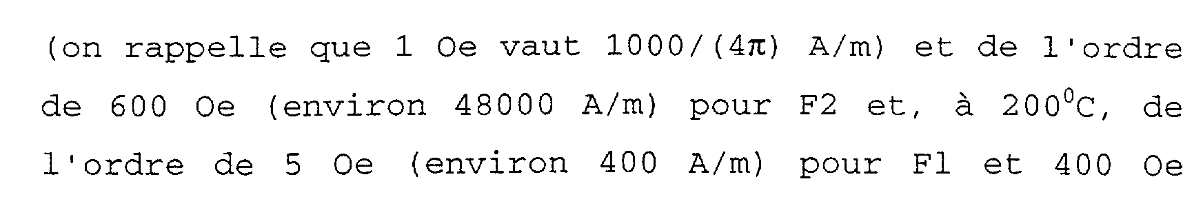
(on rappelle que 1 Oe vaut lOO0/ (4n) A/m) et de l'ordre de 600 Oe (environ 48000 A/m) pour F2 et, à 200 C, de l'ordre de 5 Oe (environ 400 A/m) pour FI et 400 Oe (environ 32000 A/m) pour F2. Typically, the materials of layers FI and F2 are chosen so that their turning fields are, at ambient temperature (approximately 20 C), of the order of 100 Oe (about 8000 A / m) for FI.
(It is recalled that 1 Oe is 100 O / (4n) A / m) and of the order of 600 Oe (about 48000 A / m) for F2 and, at 200 C, of the order of 5 Oe (about 400 A). / m) for FI and 400 Oe (about 32000 A / m) for F2.
En d'autres termes, on choisit les matériaux des couches FI et F2 de sorte que la température de blocage de l'aimantation de la couche Fl, également appelée"température de blocage magnétique" de la couche Fl ou, plus simplement,"température de blocage" de la couche FI, soit significativement plus faible que In other words, the materials of layers FI and F2 are chosen so that the magnetization blocking temperature of the layer F1, also called "magnetic blocking temperature" of the layer F1 or, more simply, "temperature blocking "of the FI layer, is significantly lower than
<Desc/Clms Page number 13><Desc / Clms Page number 13>
la température de blocage de l'aimantation de la couche F2. the blocking temperature of the magnetization of the layer F2.
Lors de l'écriture, le principe de la sélection d'un point mémoire consiste alors à provoquer un très

bref échauffement (jusqu'à une température Tmax, typiquement jusqu'à 200 C) de ce point mémoire, échauffement qui a pour effet d'abaisser le champ de retournement de l'aimantation de la couche magnétique FI dans laquelle l'information est stockée. When writing, the principle of the selection of a memory point then consists in causing a very
briefly heating (up to a temperature Tmax, typically up to 200 C) of this memory point, heating which has the effect of lowering the reversal field of the magnetization of the magnetic layer FI in which the information is stored .
Le principe de fonctionnement du dispositif étant basé sur des variations de température, il semble évident que les couches de stockage et de référence doivent de préférence avoir des températures de blocage supérieures à la température de fonctionnement du dispositif hors échauffement. Since the principle of operation of the device is based on temperature variations, it seems obvious that the storage and reference layers should preferably have blocking temperatures higher than the operating temperature of the device without heating.
De plus, le but de ce dispositif étant de stocker de l'information de façon stable, il est donc, aussi pour cette raison, préférable que ces couches aient des températures de blocage nettement supérieures à la température de fonctionnement du dispositif. In addition, the aim of this device being to store information in a stable manner, it is therefore, also for this reason, preferable for these layers to have blocking temperatures significantly higher than the operating temperature of the device.
Pendant le refroidissement du point mémoire, un champ magnétique d'amplitude He tel que
HcFl (Tmax) < He < HcF2 (Tmax),
He étant ainsi typiquement compris entre environ 20 Oe et 60 Oe (environ 1600A/m et 4800A/m), est appliqué dans la direction dans laquelle on souhaite orienter l'aimantation de la couche de stockage FI. During the cooling of the memory point, a magnetic field of amplitude He such that
HcF1 (Tmax) <He <HcF2 (Tmax),
It is thus typically between about 20 Oe and 60 Oe (about 1600A / m and 4800A / m), is applied in the direction in which it is desired to orient the magnetization of the storage layer FI.
L'aimantation de cette couche de stockage Fl s'oriente alors dans la direction du champ appliqué He alors que celle de la couche de référence F2, également The magnetization of this storage layer F1 is then oriented in the direction of the applied field He while that of the reference layer F2, also
<Desc/Clms Page number 14><Desc / Clms Page number 14>
appelée"couche piégée", reste toujours orientée dans la même direction. called "trapped layer", always remains oriented in the same direction.
L'échauffement de la jonction peut être contrôlé par l'envoi d'une brève impulsion de courant (de l'ordre de 104A/cm2 à 105A/cm2 pendant quelques nanosecondes) au travers de la jonction. The heating of the junction can be controlled by sending a short current pulse (of the order of 104 A / cm 2 at 105 A / cm 2 for a few nanoseconds) through the junction.
Le champ magnétique He est créé par l'envoi d'impulsions de courant dans des lignes conductrices situées dans des plans se trouvant au dessus et/ou au dessous des jonctions tunnel magnétiques. The magnetic field He is created by sending pulses of current in conductive lines located in planes located above and / or below the magnetic tunnel junctions.
Une deuxième possibilité pour faire commuter l'aimantation de la couche de stockage lors de son refroidissement peut consister à injecter dans cette couche un courant d'électrons dont le spin est polarisé, suivant l'une des techniques qui sont mentionnées plus loin. A second possibility for switching the magnetization of the storage layer during its cooling can consist in injecting into this layer a current of electrons whose spin is polarized, according to one of the techniques which are mentioned below.
La présente invention consiste dans ce cas à combiner l'échauffement du matériau de la couche de stockage, pour réduire le champ de retournement de l'aimantation de cette couche, avec l'application d'un couple magnétique à cette aimantation, lors du refroidissement de la couche de stockage, en faisant circuler un courant d'électrons dont le spin est polarisé à travers la couche de stockage. The present invention consists in this case of combining the heating of the material of the storage layer, in order to reduce the reversal field of the magnetization of this layer, with the application of a magnetic torque to this magnetization, during cooling. from the storage layer, by circulating a current of electrons whose spin is polarized through the storage layer.
Il est également possible de combiner la commutation, par application d'un champ local engendré par l'envoi d'un courant dans une ligne conductrice supérieure ou inférieure, avec l'injection d'un courant d'électrons à spin polarisé dans la couche de stockage de la jonction. It is also possible to combine switching, by applying a local field generated by the sending of a current in an upper or lower conductive line, with the injection of a current of spin-polarized electrons in the layer. storage of the junction.
Quatre avantages majeurs de la présente Four major advantages of this
<Desc/Clms Page number 15><Desc / Clms Page number 15>
invention peuvent être mis en avant :
1) Sélection sans faille des points mémoires : La présente invention permet une bien meilleure sélection des points mémoires que les techniques connues. En effet, supposons que les points mémoires soient organisés en un réseau carré comme on le voit sur la figure 2 qui représente l'architecture d'une mémoire MRAM connue. invention can be put forward:
1) Seamless selection of memory points: The present invention allows a much better selection of memory points than known techniques. Indeed, suppose that the memory points are organized in a square network as seen in Figure 2 which represents the architecture of a known MRAM memory.
Dans cette mémoire connue, on distingue trois niveaux de lignes : les lignes conductrices supérieures 10 qui servent à générer le champ magnétique Hx à appliquer aux jonctions tunnel magnétiques 2 lors de l'écriture et qui servent aussi de contacts électriques pour ces jonctions lors de la lecture, - les lignes conductrices inférieures 12 qui servent uniquement à générer le champ magnétique Hy au moment de l'écriture, et - les lignes de contrôle 14 qui agissent sur la grille des transistors 4 pour les mettre en position passante (saturée) ou fermée (bloquée). In this known memory, there are three levels of lines: the upper conducting lines 10 which are used to generate the magnetic field Hx to be applied to the magnetic tunnel junctions 2 during writing and which also serve as electrical contacts for these junctions when reading, - the lower conductive lines 12 which serve only to generate the magnetic field Hy at the time of writing, and - the control lines 14 which act on the gate of the transistors 4 to put them in the on (saturated) or closed position (blocked).
Selon un procédé d'écriture connu, l'écriture se fait en envoyant des impulsions de courant le long des lignes conductrices supérieure et inférieure qui se croisent au point mémoire que l'on souhaite adresser. Or, s'il existe une distribution de champ de retournement, certains points mémoires situés le long des lignes risquent de se retourner de façon incontrôlée. According to a known writing method, the writing is done by sending current pulses along the upper and lower conducting lines which intersect at the memory point which it is desired to address. However, if there is a reversal field distribution, certain memory points located along the lines risk reversing uncontrollably.
Dans la présente invention, ce problème ne se pose pas. Ceci est schématiquement illustré par la In the present invention, this problem does not arise. This is schematically illustrated by the
<Desc/Clms Page number 16><Desc / Clms Page number 16>
figure 3 où l'on voit un dispositif magnétique 16 conforme à l'invention, formant un point mémoire, ou cellule, d'une mémoire MRAM conforme à l'invention. Figure 3 where we see a magnetic device 16 according to the invention forming a memory point or cell, an MRAM memory according to the invention.
Ce point mémoire comprend une jonction tunnel magnétique 18, comportant une couche de stockage 20a, une couche de référence 20c et une couche isolante ou semiconductrice 20b entre ces dernières. Cette jonction est placée entre une ligne conductrice supérieure 22 et un transistor de commutation 24 et associée à une ligne conductrice inférieure 26 qui est perpendiculaire à la ligne 22. This memory point comprises a magnetic tunnel junction 18, comprising a storage layer 20a, a reference layer 20c and an insulating or semiconductor layer 20b therebetween. This junction is placed between an upper conductive line 22 and a switching transistor 24 and associated with a lower conductive line 26 which is perpendicular to the line 22.
En rendant passant le transistor 24 du point mémoire 16, ce transistor étant commandé par une ligne de contrôle 28, et en envoyant une impulsion de courant 30 dans la ligne conductrice supérieure 22 correspondante, cette impulsion de courant traverse la jonction 18 et provoque son échauffement. By turning on the transistor 24 of the memory point 16, this transistor being controlled by a control line 28, and by sending a current pulse 30 in the corresponding upper conductive line 22, this current pulse passes through the junction 18 and causes it to overheat. .
Or les jonctions de la mémoire de la figure 3 sont organisées en réseau carré comme dans la mémoire de la figure 2 (dont les références des éléments sont d'ailleurs suivies, entre parenthèses, des références des éléments correspondants de la figure 2). Donc seule une jonction de tout le réseau sera échauffée par l'impulsion de courant 30, toutes les autres restant à température ambiante. Now the junctions of the memory of FIG. 3 are organized in a square lattice as in the memory of FIG. 2 (whose references of the elements are moreover followed, in parentheses, by the references of the corresponding elements of FIG. 2). Thus only one junction of the entire network will be heated by the current pulse 30, all others remaining at room temperature.
L'abaissement de champ de retournement lié à l'élévation de température (typiquement de 100 Oe, à 20 C, à 5 Oe, à 200 C) est beaucoup plus important que la largeur de la distribution de champ de retournement à température ambiante (typiquement 100 Oe 20 Oe). The overturning field drop associated with the temperature rise (typically 100 Oe, at 20 C, at 5 Oe, at 200 C) is much larger than the width of the flip-flop distribution at room temperature ( typically 100 Oe 20 Oe).
En conséquence, en envoyant une impulsion de As a result, by sending a pulse of
<Desc/Clms Page number 17><Desc / Clms Page number 17>
courant 32 dans la ligne conductrice inférieure 26, ce qui génère un champ magnétique 34 de l'ordre de 10 Oe pendant le refroidissement de la jonction adressée, on est sûr de ne faire commuter que l'aimantation de la couche de stockage 20a de cette jonction. current 32 in the lower conductive line 26, which generates a magnetic field 34 of the order of 10 Oe during the cooling of the addressed junction, it is safe to switch only the magnetization of the storage layer 20a of this junction.
Cependant, la ligne 26 n'est pas indispensable pour créer le champ magnétique. On peut très bien utiliser la ligne supérieure 22 (utilisée dans un premier temps pour provoquer l'échauffement) pour générer dans un deuxième temps le champ magnétique lors du refroidissement. However, line 26 is not essential to create the magnetic field. One can very well use the upper line 22 (used firstly to cause heating) to secondly generate the magnetic field during cooling.
Dans le cas de la figure 3, si l'on supprime la ligne 26, il faut veiller à ce que les directions d'aimantation des couches soient perpendiculaires à la ligne de courant 22 génératrice du champ magnétique (par exemple en faisant pivoter le dispositif). In the case of FIG. 3, if line 26 is deleted, it is necessary to ensure that the magnetization directions of the layers are perpendicular to the current line 22 generating the magnetic field (for example by rotating the device ).
Le fonctionnement du point mémoire 16 de la figure 3 est donc le suivant : le transistor d'adressage 24 étant à l'état passant, l'écriture se fait en envoyant une impulsion de courant à travers la jonction 18 pour échauffer la jonction jusque vers 200 C. Pendant le refroidissement de la jonction, une impulsion de courant est envoyée dans la ligne conductrice inférieure 26 pour générer un champ magnétique dans la couche de stockage 20a, qui a pour effet de faire commuter l'aimantation de cette couche dans la direction désirée. The operation of the memory point 16 of FIG. 3 is therefore as follows: the addressing transistor 24 being in the on state, the writing is done by sending a current pulse through the junction 18 to heat the junction as far as C. During the cooling of the junction, a current pulse is sent in the lower conductive line 26 to generate a magnetic field in the storage layer 20a, which has the effect of switching the magnetization of this layer in the direction desired.
La lecture se fait avec le transistor à l'état bloqué en faisant circuler un courant à travers la jonction (le courant étant plus faible que lors de l'écriture pour que l'échauffement soit moindre), ce The reading is done with the transistor in the off state by circulating a current through the junction (the current being weaker than during the writing so that the heating is less), this
<Desc/Clms Page number 18><Desc / Clms Page number 18>
qui permet d'en mesurer la résistance et donc de savoir si l'aimantation de la couche de stockage 20a est parallèle ou antiparallèle à celle de la couche de référence 20c. which makes it possible to measure its resistance and therefore to know whether the magnetization of the storage layer 20a is parallel or antiparallel to that of the reference layer 20c.
2) Consommation réduite :
Compte tenu du fait que les champs à générer pour l'écriture sont beaucoup plus faibles que dans l'art antérieur (typiquement 10 Oe dans la présente invention contre 50 Oe dans l'art antérieur), l'intensité des impulsions de champ à envoyer dans les lignes conductrices est grandement réduite. 2) Reduced consumption:
Taking into account that the fields to be generated for writing are much weaker than in the prior art (typically 10 Oe in the present invention against 50 Oe in the prior art), the intensity of the field pulses to be sent in the conductive lines is greatly reduced.
De plus, une seule impulsion dans la ligne conductrice inférieure est nécessaire dans le cas de la figure 3, contre une impulsion dans la ligne conductrice inférieure et une impulsion dans la ligne conductrice supérieure dans l'art antérieur. In addition, a single pulse in the lower conductor line is required in the case of Figure 3, against a pulse in the lower conductor line and a pulse in the upper conductor line in the prior art.
La puissance nécessaire pour provoquer l'échauffement du point mémoire étant beaucoup plus faible que pour générer les impulsions de champ de 50 Oe (typiquement lpJ pour chauffer de 2000C une jonction tunnel magnétique de 150 nm x 150 nm contre plusieurs dizaines de pJ pour générer une impulsion de champ de 50 Oe le long d'une ligne de 500 points mémoires), il s'ensuit que la consommation électrique peut être divisée par 10 avec le principe de fonctionnement de la présente invention. The power required to cause the memory point to heat up being much lower than to generate the field pulses of 50 Oe (typically lpJ to heat from 2000C a magnetic tunnel junction of 150 nm x 150 nm against several tens of pJ to generate a field pulse of 50 Oe along a line of 500 memory points), it follows that the electrical consumption can be divided by 10 with the operating principle of the present invention.
3) Stabilité de l'information pour de petites dimensions :
La présente invention permet d'utiliser, pour la couche de stockage, des matériaux à forte énergie de piégeage à température ambiante. Dans l'art antérieur, 3) Information stability for small dimensions:
The present invention makes it possible to use, for the storage layer, materials with high trapping energy at ambient temperature. In the prior art,
<Desc/Clms Page number 19><Desc / Clms Page number 19>
cela n'est pas possible car plus le piégeage de la couche de stockage est important, plus il faut fournir d'énergie pour faire commuter l'aimantation de la couche de stockage. this is not possible because the higher the trapping of the storage layer, the more energy must be supplied to switch the magnetization of the storage layer.
Dans la présente invention, on abaisse l'énergie de piégeage lors de l'écriture en échauffant le matériau. On peut donc se permettre d'avoir une énergie de piégeage forte à température ambiante. Cela présente un avantage considérable pour de petites dimensions. En effet, dans l'art antérieur, l'information stockée dans la couche de stockage devient instable par rapport aux fluctuations thermiques à température ambiante. In the present invention, the trapping energy is lowered during writing by heating the material. We can therefore afford to have a strong trapping energy at room temperature. This has a considerable advantage for small dimensions. Indeed, in the prior art, the information stored in the storage layer becomes unstable with respect to thermal fluctuations at room temperature.
En effet, si K et V désignent respectivement l'anisotropie magnétique par unité de volume (ou, plus généralement, l'énergie de piégeage par unité de volume) et le volume de la couche de stockage, l'information devient instable si KV < 25kT (où k est la constante de Boltzmann et T la température). Indeed, if K and V respectively designate the magnetic anisotropy per unit of volume (or, more generally, the trapping energy per unit of volume) and the volume of the storage layer, the information becomes unstable if KV < 25kT (where k is the Boltzmann constant and T the temperature).
Pour un matériau donné, cette limite est toujours atteinte à un moment ou à un autre lorsqu'on diminue la taille du point mémoire alors que, dans la présente invention, on peut très bien compenser la diminution du volume par une augmentation de l'énergie de piégeage à température ambiante et donc réduire la taille du point mémoire autant que le permet le procédé de fabrication (par exemple lithographie/gravure) utilisé. For a given material, this limit is always reached at one time or another when the size of the memory point is reduced while, in the present invention, it is very well possible to compensate the decrease of the volume by an increase of the energy. trapping at room temperature and therefore reduce the size of the memory point as much as the manufacturing method (eg lithography / etching) used.
4) Simplicité de la réalisation si l'on utilise comme principe de commutation un échauffement plus une injection d'un courant d'électrons à spin 4) Simplicity of the realization if one uses as switching principle a heating more an injection of a current of spin electrons
<Desc/Clms Page number 20><Desc / Clms Page number 20>
polarisé :
En effet, il n'y a pas besoin, dans ce cas, de rajouter un niveau de lignes pour la génération des champs magnétiques locaux. La réalisation de l'ensemble des. points mémoires s'en trouve simplifiée, ce qui peut permettre d'atteindre des densités d'intégration supérieures. polarized:
Indeed, there is no need, in this case, to add a level of lines for the generation of local magnetic fields. The achievement of all. memory points are thereby simplified, which can make it possible to achieve higher integration densities.
On reviendra plus loin sur l'utilisation, dans la présente invention, d'un courant d'électrons à spin polarisé. Reference will be made later to the use, in the present invention, of a polarized spin electron current.
On considère, dans ce qui suit, divers exemples de l'invention. Various examples of the invention are considered in the following.
Comme on l'a vu plus haut, la structure de base, dans la présente invention, comporte deux couches magnétiques Fl et F2 séparées par une barrière tunnel 0 de sorte que l'on peut noter cette structure Fl/O/F2. As we have seen above, the basic structure in the present invention comprises two magnetic layers F1 and F2 separated by a tunnel barrier 0 so that this structure F1 / O / F2 can be noted.
Les deux couches magnétiques sont telles que le champ de retournement de l'aimantation de l'une de ces deux couches magnétiques (la couche de stockage) décroît beaucoup plus vite, lorsque la température augmente, que celui de l'autre couche magnétique (la couche de référence). The two magnetic layers are such that the reversal field of the magnetization of one of these two magnetic layers (the storage layer) decreases much more rapidly, when the temperature increases, than that of the other magnetic layer (the reference layer).
Dans un premier mode de réalisation de l'invention, les aimantations des deux couches Fl et F2 sont perpendiculaires au plan des couches ou, plus précisément, aux interfaces de ces couches. In a first embodiment of the invention, the magnetizations of the two layers F1 and F2 are perpendicular to the plane of the layers or, more specifically, to the interfaces of these layers.
Des couches Fl et F2 peuvent être constituées d'un matériau pur, d'un alliage ou d'un ensemble de couches alternées dont certaines sont magnétiques. Fl and F2 layers may consist of a pure material, an alloy or a set of alternating layers some of which are magnetic.
Des couches de Co, de structure hexagonale, ont leur aimantation perpendiculaire au plan de ces couches Co layers, of hexagonal structure, have their magnetization perpendicular to the plane of these layers
<Desc/Clms Page number 21><Desc / Clms Page number 21>
si l'axe c de la maille hexagonale est perpendiculaire au plan de l'échantillon contenant ces couches. Des couches en alliages tels que CoPt, FePd et FePt peuvent aussi avoir des aimantations perpendiculaires à leur plan. Enfin, des multicouches comprenant une alternance de couches de deux matériaux différents dont au moins l'un est magnétique, comme par exemple Co 0,6nm/Pt l, 4nm, peuvent aussi avoir des aimantations perpendiculaires au plan. if the c axis of the hexagonal mesh is perpendicular to the plane of the sample containing these layers. Alloyed layers such as CoPt, FePd and FePt may also have magnetizations perpendicular to their plane. Finally, multilayers comprising an alternation of layers of two different materials of which at least one is magnetic, such as Co 0.6nm / Pt l, 4nm, may also have magnetizations perpendicular to the plane.
Le cobalt peut être aisément remplacé par un alliage riche en Co (supérieur à 70%) avec par exemple du Fe ou du Ni ou du Cr. Cobalt can be easily replaced by an alloy rich in Co (greater than 70%) with for example Fe or Ni or Cr.
Un exemple de réalisation d'une jonction tunnel magnétique à base de multicouches Co/Pt, qui est utilisable dans la présente invention, est montré sur la figure 4. An exemplary embodiment of a Co / Pt multilayer magnetic tunnel junction, which is usable in the present invention, is shown in FIG.
Plus précisément, comme on le voit sur la figure 4, cette jonction tunnel magnétique comprend une couche de référence 36 et une couche de stockage 38 qui ont une aimantation perpendiculaire au plan de ces couches ; la couche de référence 36 comprend des couches 40 en cobalt qui alternent avec des couches 42 en platine ; de même, la couche de stockage 38 comprend des couches 44 en cobalt qui alternent avec des couches 46 en platine ; les couches 36 et 38 sont séparées par une couche de barrière tunnel 48 en alumine. More precisely, as can be seen in FIG. 4, this magnetic tunnel junction comprises a reference layer 36 and a storage layer 38 which have a magnetization perpendicular to the plane of these layers; the reference layer 36 comprises layers 40 of cobalt which alternate with layers 42 of platinum; similarly, the storage layer 38 comprises layers 44 of cobalt which alternate with layers 46 of platinum; layers 36 and 38 are separated by a tunnel barrier layer 48 of alumina.
En jouant sur les épaisseurs relatives de Co et de Pt, on peut faire varier la coercitivité du matériau constitutif de chacune des couches 36 et 38 ainsi que la variation de cette coercitivité en fonction de la température. On peut aussi augmenter l'énergie de By varying the relative thicknesses of Co and Pt, it is possible to vary the coercivity of the material constituting each of the layers 36 and 38 as well as the variation of this coercivity as a function of the temperature. We can also increase the energy of
<Desc/Clms Page number 22><Desc / Clms Page number 22>
piégeage de l'aimantation de l'une des couches (la couche de référence 36) en la couplant à un matériau antiferromagnétique 50 à forte température de blocage, comme PtMn ou PtPdMn. trapping the magnetization of one of the layers (the reference layer 36) by coupling it to an antiferromagnetic material 50 with a high blocking temperature, such as PtMn or PtPdMn.
Dans ce cas, la couche ferromagnétique adjacente voit la valeur de sa température de blocage augmenter jusqu'à la valeur de celle de la couche antiferromagnétique. In this case, the adjacent ferromagnetic layer sees the value of its blocking temperature increase to the value of that of the antiferromagnetic layer.
D'autres exemples de multicouches à anisotropie perpendiculaire, utilisables dans l'invention, sont par exemple Co/Pd, Co/Ni, Cu/Ni. Other examples of multilayers with perpendicular anisotropy, which can be used in the invention, are for example Co / Pd, Co / Ni, Cu / Ni.
A titre d'exemple, la figure 5 montre qu'on peut obtenir une structure à aimantation perpendiculaire au plan, qui associe deux multicouches de coercivités différentes. By way of example, FIG. 5 shows that it is possible to obtain a magnetization structure perpendicular to the plane, which associates two multilayers of different coercivities.
On a tracé les variations de la magnétorésistance MR (en%) en fonction du champ magnétique appliqué H (en kOe) pour la structure Ni0300/C06/ (Pt18/C06) 2/CU30/ (C06/Pt18) 2. Magnetoresistance MR (in%) variations were plotted against the applied magnetic field H (in kOe) for the structure Ni0300 / C06 / (Pt18 / CO6) 2 / CU30 / (CO6 / Pt18) 2.
Dans le cas de la figure 5, l'augmentation de coercitivité de l'une des multicouches est obtenue en couplant l'aimantation de cette multicouche a une couche antiferromagnétique adjacente (par exemple NiO (cas de la figure 5), PtMn, PdPtMn ou FeMn). In the case of FIG. 5, the increase in coercivity of one of the multilayers is obtained by coupling the magnetization of this multilayer to an adjacent antiferromagnetic layer (for example NiO (case of FIG. 5), PtMn, PdPtMn or FeMn).
Le même résultat pourrait être obtenu en associant une multicouche de Co/Pt à un alliage de FePt. The same result could be obtained by combining a Co / Pt multilayer with an FePt alloy.
Par ailleurs, chacun des matériaux précités a sa propre variation de champ coercitif en fonction de la température. Furthermore, each of the aforementioned materials has its own variation in coercive field as a function of temperature.
La figure 6 montre par exemple les variations Figure 6 shows for example the variations
<Desc/Clms Page number 23><Desc / Clms Page number 23>
du champ de retournement Hr (en Oe) d'une multicouche (Co 0,6nm/Pt 1, 4nm) en fonction de la température T (en OC) pour une plaque"pleine tranche", de dimension latérale macroscopique (courbe I), et dans des réseaux (en anglais"arrays") de plots de dimensions submicroniques (courbe II). of the reversal field Hr (in Oe) of a multilayer (Co 0.6nm / Pt 1, 4nm) as a function of the temperature T (in OC) for a "full slice" plate, of macroscopic lateral dimension (curve I) , and in arrays of plots of submicron dimensions (curve II).
Pour les épaisseurs de Co et de Pt utilisées, le champ de retournement Hr décroît rapidement avec la température pour quasiment s'annuler à une température
![]()
Tc de l'ordre de 200 C. For the thicknesses of Co and Pt used, the reversal field Hr decreases rapidly with temperature and almost vanishes at a temperature
![]()
Tc of the order of 200 C.
Si l'on augmente l'épaisseur de Co à épaisseur de Pt fixe, le champ de retournement décroît moins vite, c'est à dire s'annule à une température supérieure à 200 C. De même, dans l'alliage FePt, le champ de retournement s'annule vers 500 C. If we increase the thickness of Co with a fixed Pt thickness, the reversal field decreases less rapidly, ie vanishes at a temperature greater than 200 C. Similarly, in the FePt alloy, the turnaround field vanishes towards 500 C.
Donc en réalisant par exemple une jonction tunnel magnétique qui associe une multicouche, formée d'une alternance de couches de Co et de couches de Pt, avec une électrode en alliage FePt, on réalise une structure conforme à l'invention. En envoyant une impulsion de courant à travers la jonction, on élève la température de cette dernière jusque vers 200 C. Therefore by making, for example, a magnetic tunnel junction which associates a multilayer, formed by alternating layers of Co and layers of Pt, with an electrode of FePt alloy, a structure is produced in accordance with the invention. By sending a current pulse through the junction, the temperature of the latter is raised to around 200 C.
On coupe alors le courant qui circulait à travers la jonction et, pendant le refroidissement de cette jonction, on applique un faible champ magnétique à l'aide de lignes conductrices inférieures ou supérieures (voir la figure 7). L'aimantation de la couche de référence demeure inchangée alors que celle de la couche de stockage s'oriente dans la direction du champ appliqué pendant le refroidissement. The current flowing through the junction is then cut off and, during the cooling of this junction, a weak magnetic field is applied using lower or higher conductive lines (see Figure 7). The magnetization of the reference layer remains unchanged while that of the storage layer is oriented in the direction of the applied field during cooling.
Plus précisément, la figure 7 illustre un More specifically, Figure 7 illustrates a
<Desc/Clms Page number 24><Desc / Clms Page number 24>
exemple de réalisation d'un ensemble de plusieurs points mémoires à partir de jonctions tunnel à aimantation perpendiculaire au plan selon la présente invention. Ces jonctions 52a, 52b, 52c et 52d comprennent chacune une couche de référence 54, une couche de stockage 56 et, entre celles-ci, une couche isolante ou semiconductrice 58. Ces jonctions 52a, 52b, 52c et 52d sont comprises entre des transistors de commutation 60a, 60b, 60c et 60d et une ligne conductrice 62. exemplary embodiment of a set of several memory points from magnetization tunnel junctions perpendicular to the plane according to the present invention. These junctions 52a, 52b, 52c and 52d each comprise a reference layer 54, a storage layer 56 and, between them, an insulating or semiconductive layer 58. These junctions 52a, 52b, 52c and 52d are between transistors 60a, 60b, 60c and 60d and a conductive line 62.
On voit aussi des lignes conductrices supérieures, telle que les lignes 64,66 et 68, qui sont situées de part et d'autre des jonctions. Higher conductive lines, such as lines 64, 66 and 68, which are located on either side of the junctions, are also seen.
Pour l'écriture d'un point mémoire, par exemple celui qui comprend la jonction 52b, cette jonction est chauffée au dessus de la température de blocage de la couche de stockage mais en dessous de la température de blocage de la couche de référence par l'envoi d'une impulsion à travers la jonction. For the writing of a memory point, for example that which comprises the junction 52b, this junction is heated above the blocking temperature of the storage layer but below the blocking temperature of the reference layer by sending an impulse through the junction.
De plus, les transistors sont mis à l'état bloqué sauf le transistor 60b associé à la jonction 52b, qui est mis à l'état passant. In addition, the transistors are put in the off state except the transistor 60b associated with the junction 52b, which is put in the on state.
Les deux lignes conductrices supérieures 64 et 66 situées de part et d'autre de la jonction à adresser 52b sont alimentées par des courants sensiblement opposés pour créer deux champs magnétiques 70 et 72 sensiblement perpendiculaires au plan, qui s'ajoutent au niveau de la jonction à adresser. Ces champs servent à polariser l'aimantation de la couche de stockage pendant son refroidissement en dessous de sa température de blocage. L'aimantation de la couche de The two upper conductive lines 64 and 66 located on either side of the junction to be addressed 52b are powered by currents substantially opposite to create two magnetic fields 70 and 72 substantially perpendicular to the plane, which are added at the junction to address. These fields serve to bias the magnetization of the storage layer during its cooling below its blocking temperature. The magnetization of the layer of
<Desc/Clms Page number 25><Desc / Clms Page number 25>
stockage peut prendre ici deux états (stockage binaire). storage can take two states here (binary storage).
Une deuxième méthode pour réaliser la commutation lors du refroidissement consiste à injecter un courant d'électrons à spin polarisé à travers la couche de stockage. Une structure permettant de réaliser cette opération est représentée sur la figure 8. A second method for switching during cooling consists in injecting a current of spin-polarized electrons through the storage layer. A structure enabling this operation to be carried out is shown in FIG. 8.
Sur cette figure 8, on voit un empilement 74 compris entre une ligne conductrice supérieure 76 et un transistor de commutation 78. L'empilement comprend, en allant de la ligne 76 au transistor 78, une couche 80 en PtMn, une couche de référence 82, une couche d'alumine 84, une couche de stockage 86, une couche de cuivre 88, une couche 90 dite"polarisante"et une couche 92 en PtMn. In this FIG. 8, a stack 74 is seen between an upper conductive line 76 and a switching transistor 78. The stack comprises, going from line 76 to transistor 78, a layer 80 made of PtMn, a reference layer 82 , a layer of alumina 84, a storage layer 86, a copper layer 88, a so-called "polarizing" layer 90 and a layer 92 made of PtMn.
La couche de stockage 86 est constituée ici d'un matériau à aimantation perpendiculaire dont le champ de retournement s'annule vers 2000C tel que par exemple une multicouche (Co/Pt). La couche de référence 82 est constituée d'un matériau dont le champ de retournement et l'aimantation restent importants à 200 C, comme par exemple FePt. De même, l'aimantation de la deuxième couche magnétique de FePt formant la couche polarisante 90 reste importante à 200 C. The storage layer 86 here consists of a material with perpendicular magnetization whose reversal field is canceled out around 2000C such as for example a multilayer (Co / Pt). The reference layer 82 consists of a material whose reversal field and the magnetization remain significant at 200 C, such as for example FePt. Likewise, the magnetization of the second magnetic layer of FePt forming the polarizing layer 90 remains significant at 200 C.
Le principe de la commutation magnétique est le suivant : on applique une impulsion de courant soit de haut en bas soit de bas en haut à travers la jonction tunnel. The principle of magnetic switching is as follows: a current pulse is applied either from top to bottom or from bottom to top through the tunnel junction.
Cette impulsion de courant a un profil particulier : elle monte à sa valeur maximum en un temps This current pulse has a particular profile: it rises to its maximum value in a time
<Desc/Clms Page number 26> <Desc / Clms Page number 26>

de l'ordre de lns à quelques nanosecondes puis redescend progressivement à zéro en quelques nanosecondes. Cette impulsion de courant a pour effet, dans un premier temps, d'échauffer la jonction puis, dans un deuxième temps, lors de la décroissance du courant c'est à dire lors du refroidissement de la jonction, d'orienter l'aimantation dans une direction particulière.
of the order of lns to a few nanoseconds and then progressively drops back to zero in a few nanoseconds. This current pulse has the effect, at first, of heating the junction and then, in a second step, during the decay of the current that is to say during the cooling of the junction, to orient the magnetization in a particular direction.
Si le courant circule de haut en bas (c'est à dire si les électrons circulent de bas en haut), des électrons à spin polarisé vers le bas sont injectés dans la multicouche de Co/Pt. De plus, les électrons qui vont traverser par effet tunnel la barrière d'alumine 84 sont préférentiellement des électrons dont le spin est parallèle à l'aimantation de la couche 82 de FePt et sont donc des électrons à spin vers le haut . If the current flows from top to bottom (ie if the electrons flow from bottom to top), electrons with spin polarized downwards are injected into the multilayer of Co / Pt. In addition, the electrons which will tunnel through the alumina barrier 84 are preferably electrons whose spin is parallel to the magnetization of the layer 82 of FePt and are therefore electrons with upward spin.
Cela va générer, dans la multicouche de Co/Pt, un excès d'électrons vers le bas. Cet excès d'électrons vers le bas, cumulé avec l'injection d'électrons vers le bas en provenance de la couche polarisante inférieure, va forcer l'aimantation de la multicouche de Co/Pt à s'orienter vers le bas lors de son refroidissement. This will generate, in the Co / Pt multilayer, an excess of electrons downwards. This excess of electrons downwards, accumulated with the injection of electrons downwards from the lower polarizing layer, will force the magnetization of the Co / Pt multilayer to move downwards during its cooling.
Au contraire, si le courant circule de bas en haut (c'est à dire si les électrons circulent de haut en bas), il va y avoir accumulation d'électrons vers le haut dans la couche de Co/Pt, ce qui aura pour effet de forcer l'aimantation de cette couche à s'orienter vers le haut lors de son refroidissement. On the contrary, if the current flows from bottom to top (ie if the electrons flow from top to bottom), there will be accumulation of electrons upwards in the layer of Co / Pt, which will have effect of forcing the magnetization of this layer to move upwards during its cooling.
Précisons que ce principe de commutation Note that this switching principle
<Desc/Clms Page number 27><Desc / Clms Page number 27>
magnétique pourrait fonctionner également sans la couche polarisante inférieure mais la forme de l'impulsion de courant serait alors plus difficile à ajuster pour trouver un bon équilibre entre une réduction du courant suffisante pour que la température de la jonction baisse suffisamment et une circulation de courant suffisante pour arriver à polariser l'aimantation de la couche de stockage lors de son refroidissement. magnetic could also work without the lower polarizing layer but the shape of the current pulse would then be more difficult to adjust to find a good balance between a reduction of the current sufficient for the temperature of the junction to drop sufficiently and a circulation of current sufficient to polarize the magnetization of the storage layer during its cooling.
L'intérêt de la couche polarisante supplémentaire 90 est de permettre de cumuler le courant d'électrons à spin polarisé provenant de l'autre couche 82 de la jonction tunnel et le courant d'électrons à spin polarisé provenant de la couche polarisante 90. The advantage of the additional polarizing layer 90 is that it allows the polarized spin electron current from the other layer 82 of the tunnel junction to be accumulated and the polarized spin electron current from the polarizing layer 90.
Cette structure du point mémoire est particulièrement simple puisqu'elle ne nécessite, en plus du transistor d'adressage et de la jonction tunnel, qu'un niveau de ligne conductrice. This structure of the memory point is particularly simple since it requires, in addition to the addressing transistor and the tunnel junction, a conductive line level.
Dans un deuxième mode de réalisation de l'invention, les aimantations des deux couches Fl et F2 sont parallèles au plan des couches ou, plus précisément, aux interfaces de ces couches. In a second embodiment of the invention, the magnetizations of the two layers F1 and F2 are parallel to the plane of the layers or, more specifically, to the interfaces of these layers.
Comme précédemment, les matériaux magnétiques constitutifs de la jonction tunnel magnétique doivent être choisis de sorte que l'un présente une décroissance thermique de son champ coercitif plus rapide que l'autre. As before, the magnetic materials constituting the magnetic tunnel junction must be chosen so that one exhibits a thermal decrease in its coercive field faster than the other.
Le matériau de la couche F2 de référence peut être en alliage à base de Co, Fe, Ni (par exemple C09OFelO) et son aimantation peut être piégée par The material of the reference layer F2 can be an alloy based on Co, Fe, Ni (for example C09OFelO) and its magnetization can be trapped by
<Desc/Clms Page number 28><Desc / Clms Page number 28>
interaction d'échange avec un matériau antiferromagnétique à forte température de blocage (très supérieure à 200 C) comme PtMn. exchange interaction with an antiferromagnetic material with a high blocking temperature (much higher than 200 C) such as PtMn.
Le matériau de la couche Fl peut être constitué d'un alliage dont la température de Curie est réduite en volume pour permettre de faciliter le basculement de son aimantation lorsque ce matériau est chauffé vers 200 C. The material of the layer F1 can consist of an alloy whose Curie temperature is reduced in volume to allow easier tilting of its magnetization when this material is heated to around 200 C.
Un mode avantageux de réalisation de cette propriété consiste à coupler l'aimantation de la couche de stockage à une couche antiferromagnétique à faible température de blocage (par exemple FesoMngo ou IrzoMngo dont la température de blocage est inférieure à 2000C tandis que l'aimantation de l'autre couche magnétique (la couche de référence) est couplée à un matériau antiferromagnétique à forte température de blocage, par exemple PtMn dont la température de blocage est supérieure à 280 C. An advantageous embodiment of this property consists in coupling the magnetization of the storage layer to an antiferromagnetic layer with a low blocking temperature (for example FesoMngo or IrzoMngo whose blocking temperature is less than 2000C while the magnetization of the Another magnetic layer (the reference layer) is coupled to antiferromagnetic material with a high blocking temperature, for example PtMn whose blocking temperature is greater than 280.degree.
Ceci est schématiquement illustré par la figure 9 où l'on voit un exemple de jonction tunnel à aimantation planaire utilisable dans la présente invention. This is schematically illustrated in FIG. 9 where we see an example of tunnel junction with planar magnetization usable in the present invention.
La couche de référence 94 en C09oFelO est piégée par interaction avec une couche antiferromagnétique 96 à haute température de blocage (très supérieure à 200 C), par exemple en PtMn ou en NiMn. The reference layer 94 in C09oFelO is trapped by interaction with an antiferromagnetic layer 96 at high blocking temperature (much higher than 200 C), for example in PtMn or in NiMn.
La couche de stockage 98 en NigoFeso est couplée à une couche antiferromagnétique 100 à faible température de blocage (compris entre 1000C et 200 C), par exemple en FE50Mn50 ou en Ir2oMnso et cette couche 98 est séparée de la couche 94 par une couche de barrière The storage layer 98 in NigoFeso is coupled to an antiferromagnetic layer 100 at low blocking temperature (between 1000C and 200 C), for example in FE50Mn50 or Ir2oMnso and this layer 98 is separated from layer 94 by a barrier layer
<Desc/Clms Page number 29><Desc / Clms Page number 29>
tunnel 102 en A1203. tunnel 102 in A1203.
Notons qu'une façon de faire baisser la température de blocage de la couche antiferromagnétique couplée à la couche de stockage peut être de diminuer son épaisseur. On sait en effet que plus une couche antiferromagnétique est mince, plus sa température de blocage est basse. Note that one way to lower the blocking temperature of the antiferromagnetic layer coupled to the storage layer may be to reduce its thickness. Indeed, it is known that the thinner antiferromagnetic layer, the lower its blocking temperature.
L'écriture de l'information se fait comme précédemment en envoyant une impulsion de courant à travers la jonction, impulsion qui a pour effet d'échauffer le matériau de la couche de stockage (comprenant la couche antiferromagnétique adjacente) à une température permettant le retournement de l'aimantation de cette couche, alors que la couche de référence reste à une température suffisamment faible pour que son aimantation reste fixe. The writing of the information is done as before by sending a pulse of current through the junction, a pulse that has the effect of heating the material of the storage layer (comprising the adjacent antiferromagnetic layer) to a temperature allowing the reversal the magnetization of this layer, while the reference layer remains at a sufficiently low temperature so that its magnetization remains fixed.
Ceci est schématiquement illustré par la figure 10 où l'on voit un exemple de réalisation d'un point mémoire à partir d'une jonction tunnel à aimantation planaire conformément à la présente invention. This is schematically illustrated in FIG. 10 where an exemplary embodiment of a memory point is seen from a tunnel junction with planar magnetization in accordance with the present invention.
Pour l'écriture, la jonction est chauffée au dessus de la température de blocage de la couche de stockage 98 mais en dessous de la température de blocage de la couche de référence 94, par l'envoi d'une impulsion de courant à travers la jonction, cette impulsion se propageant de la ligne conductrice 104 au transistor 106, qui est alors rendu passant. For writing, the junction is heated above the blocking temperature of the storage layer 98 but below the blocking temperature of the reference layer 94, by sending a current pulse through the junction, this pulse propagating from the conductive line 104 to the transistor 106, which is then turned on.
La ligne conductrice supérieure 108 sert à créer le champ magnétique 110 qui polarise l'aimantation de la couche de stockage 98 dans la direction désirée pendant son refroidissement. Cette The upper conductive line 108 serves to create the magnetic field 110 which polarizes the magnetization of the storage layer 98 in the desired direction during its cooling. This
<Desc/Clms Page number 30><Desc / Clms Page number 30>
aimantation de la couche de stockage ne peut prendre ici que deux états (stockage binaire). Magnetization of the storage layer can only take two states here (binary storage).
Pour des raisons déjà données plus haut à propos d'autres exemples, la ligne 108 n'est pas obligatoire : sa fonction peut être avantageusement réalisée par la ligne 104. Dans ce cas, il faut aussi veiller à ce que les directions d'aimantation des couches soient orthogonales à la direction de la ligne 104. For reasons already given above with respect to other examples, line 108 is not compulsory: its function can advantageously be performed by line 104. In this case, it is also necessary to ensure that the directions of magnetization layers are orthogonal to the direction of line 104.
Ce dispositif, dans lequel la couche de stockage est couplée à une couche antiferromagnétique dont la température de blocage est plus faible que la couche de référence, présente deux avantages majeurs :
1) La limite superparamagnétique de stabilité de la couche de stockage est repoussée de sorte que l'on peut réaliser des points mémoires de taille plus petite en utilisant cette technique. This device, in which the storage layer is coupled to an antiferromagnetic layer whose blocking temperature is lower than the reference layer, has two major advantages:
1) The superparamagnetic limit of stability of the storage layer is pushed back so that smaller size memory points can be made using this technique.
En effet, un problème qui apparaît toujours dans le stockage de l'information magnétique dans des points mémoires de petites dimensions (échelle submicronique) est celui de la stabilité de l'aimantation vis à vis des fluctuations thermiques (limite superparamagnétique). Indeed, a problem that always appears in the storage of magnetic information in small memory points (submicron scale) is that of the stability of the magnetization with respect to thermal fluctuations (superparamagnetic limit).
Si K désigne l'anisotropie magnétique du matériau et V le volume de la couche magnétique de stockage, le temps caractéristique de renversement de l'aimantation par passage au dessus de la barrière d'énergie de hauteur KV est T=l : oexp (KV/ (kT)) où To est un temps caractéristique d'essai de l'ordre de 10-9 seconde, k la constante de Boltzman et T la température. If K denotes the magnetic anisotropy of the material and V the volume of the magnetic storage layer, the characteristic time of reversal of the magnetization by passage above the energy barrier of height KV is T = l: oexp (KV / (kT)) where To is a characteristic test time of the order of 10-9 seconds, k the Boltzman constant and T the temperature.
<Desc/Clms Page number 31> <Desc / Clms Page number 31>
Pour que l'information que l'on écrit dans la couche de stockage reste stable pendant au moins 10 ans, il faut que l'aimantation elle-même reste stable pendant cette durée. Il faut donc que TT'TT' - > Log (10ans/10s) c'est-à-dire : KV > 40kT. kT
Ceci impose une limite minimale au volume de la couche de stockage et donc à sa dimension latérale, c'est à dire une limite minimale à la dimension du point mémoire. In order for the information that we write in the storage layer to remain stable for at least 10 years, the magnetization itself must remain stable during this period. It is therefore necessary that TT'TT '-> Log (10years / 10s), that is to say: KV> 40kT. kT
This imposes a minimum limit on the volume of the storage layer and therefore on its lateral dimension, that is to say a minimum limit on the dimension of the memory point.
Par contre, si la couche magnétique de stockage est couplée à une couche antiferromagnétique dont l'anisotropie est relativement forte à température ambiante mais décroît rapidement lorsqu'on approche de la température de blocage de cette couche (vers 200 C), alors la limite superparamagnétique est repoussée. On the other hand, if the magnetic storage layer is coupled to an antiferromagnetic layer whose anisotropy is relatively strong at ambient temperature but decreases rapidly when approaching the blocking temperature of this layer (around 200 ° C.), then the superparamagnetic limit is repulsed.
En effet, la barrière d'énergie à franchir pour retourner l'aimantation de la couche de stockage à température ambiante vaut maintenant A (KfEf + KaEa) où A désigne l'aire commune à la couche magnétique de stockage et à la couche antiferromagnétique, Ef et Ea désignent respectivement les épaisseurs de ces couches de stockage et antiferromagnétique et KE et Ka désignent respectivement leurs anisotropies magnétiques. Indeed, the energy barrier to be crossed to return the magnetization of the storage layer to ambient temperature is now A (KfEf + KaEa) where A denotes the common area of the storage magnetic layer and the antiferromagnetic layer, Ef and Ea respectively denote the thicknesses of these storage and antiferromagnetic layers and KE and Ka respectively denote their magnetic anisotropies.
Comme l'anisotropie Ka du matériau antiferromagnétique est habituellement beaucoup plus forte que celle (Kf) de la couche ferromagnétique de stockage à température ambiante, il apparaît que la condition de stabilité A (KfEf + KaEa) > 40kT pourra être satisfaite pour des dimensions beaucoup plus petites que si la couche magnétique de stockage était seule. As the anisotropy Ka of the antiferromagnetic material is usually much stronger than that (Kf) of the ferromagnetic storage layer at room temperature, it appears that the condition of stability A (KfEf + KaEa)> 40kT can be satisfied for dimensions much smaller than if the magnetic storage layer were alone.
<Desc/Clms Page number 32> <Desc / Clms Page number 32>
Typiquement, le terme KaEa peut être 100 fois plus grand à température ambiante que le terme KfEf. Typically, the term KaEa can be 100 times larger at room temperature than the term KfEf.
Ceci implique que l'aire de la jonction peut être 100 fois plus petite tout en restant au dessus de la limite superparamagnétique. Ceci permet donc d'atteindre des densités d'intégration beaucoup plus fortes. This implies that the area of the junction can be 100 times smaller while remaining above the superparamagnetic limit. This makes it possible to achieve much higher integration densities.
Précisons qu'il est également possible d'utiliser ce couplage de la couche de stockage à une couche antiferromagnétique à faible température de Néel dans le cas précédemment décrit de couches magnétiques à aimantation perpendiculaire au plan. Là aussi, la limite superparamagnétique sera repoussée vers les plus petites dimensions à température ambiante. Note that it is also possible to use this coupling of the storage layer to a low temperature antiferromagnetic Néel layer in the previously described case of magnetic magnetization layers perpendicular to the plane. Here too, the superparamagnetic limit will be pushed back to the smallest dimensions at room temperature.
2) Le deuxième avantage très important résultant de l'utilisation d'une couche de stockage couplée à une couche antiferromagnétique est de pouvoir réaliser un stockage de l'information multiniveaux. 2) The second very important advantage resulting from the use of a storage layer coupled with an antiferromagnetic layer is to be able to carry out a multilevel information storage.
En effet, avec les jonctions de l'art antérieur, un point mémoire a deux états possibles qui correspondent aux deux configurations magnétiques parallèle et antiparallèle, ces dernières correspondant respectivement à des alignements parallèle et antiparallèle de l'aimantation de la couche de stockage par rapport à celle de la couche de référence. Indeed, with the junctions of the prior art, a memory point has two possible states which correspond to the two parallel and antiparallel magnetic configurations, the latter corresponding respectively to parallel and antiparallel alignments of the magnetization of the storage layer with respect to to that of the reference layer.
Ces systèmes de type bistables sont obtenus en donnant à la couche de stockage une anisotropie magnétique d'origine magnétocristalline ou de forme (point mémoire par exemple de forme elliptique), avec un axe facile d'aimantation parallèle à l'aimantation de la couche de référence. These bistable type systems are obtained by giving the storage layer a magnetic anisotropy of magnetocrystalline origin or shape (memory point for example of elliptical shape), with an easy axis of magnetization parallel to the magnetization of the layer of reference.
Dans la présente invention, l'aimantation de la In the present invention, the magnetization of the
<Desc/Clms Page number 33><Desc / Clms Page number 33>
couche de stockage peut être avantageusement orientée dans n'importe quelle direction intermédiaire entre la direction parallèle et la direction antiparallèle à l'aimantation de la couche de référence. The storage layer may be advantageously oriented in any intermediate direction between the parallel direction and the direction antiparallel to the magnetization of the reference layer.
Pour ce faire, il suffit de chauffer la couche de stockage et la couche antiferromagnétique adjacente au dessus de la température de blocage de cette couche, en envoyant une impulsion de courant à travers la jonction, puis d'orienter l'aimantation de la couche de stockage dans la direction désirée au cours du refroidissement de la couche antiferromagnétique. To do this, it is sufficient to heat the storage layer and the adjacent antiferromagnetic layer above the blocking temperature of this layer, by sending a pulse of current through the junction, and then to orient the magnetization of the layer of storage in the desired direction during cooling of the antiferromagnetic layer.
Pour donner l'orientation désirée à l'aimantation de la couche de stockage, il faut appliquer un champ magnétique local à cette dernière dans la direction désirée. Pour ce faire, deux possibilités existent :
1) On peut utiliser une architecture dans laquelle la commutation magnétique s'effectue en envoyant des impulsions de courant dans des lignes conductrices perpendiculaires qui sont respectivement situées au dessus et en dessous de ce point mémoire. To give the desired orientation to the magnetization of the storage layer, it is necessary to apply a local magnetic field to the latter in the desired direction. To do this, two possibilities exist:
1) An architecture can be used in which magnetic switching is effected by sending current pulses in perpendicular conductive lines which are respectively above and below this memory point.
Ces lignes permettent de générer des champs magnétiques suivant deux directions perpendiculaires. En jouant sur l'intensité relative du courant circulant dans les deux lignes, on peut générer un champ magnétique dans n'importe quelle direction du plan. These lines make it possible to generate magnetic fields in two perpendicular directions. By playing on the relative intensity of the current flowing in the two lines, one can generate a magnetic field in any direction of the plane.
Ceci est schématiquement illustré par la figure 11 qui montre un exemple de réalisation d'un point mémoire à partir d'une jonction tunnel à aimantation planaire conformément à la présente invention. This is schematically illustrated in Figure 11 which shows an exemplary embodiment of a memory point from a planar magnetization tunnel junction in accordance with the present invention.
Pour l'écriture, la jonction tunnel magnétique For writing, the magnetic tunnel junction
<Desc/Clms Page number 34><Desc / Clms Page number 34>
est chauffée au dessus de la température de blocage de la couche de stockage 112 mais en dessous de la température de blocage de la couche de référence 114, par l'envoi d'une impulsion de courant à travers la jonction. is heated above the blocking temperature of the storage layer 112 but below the blocking temperature of the reference layer 114, by sending a current pulse through the junction.
Les lignes conductrices supérieure 116 et inférieure 118 servent à créer des champs magnétiques 120 et 122 suivant deux directions perpendiculaires dans le plan, qui permettent de polariser l'aimantation de la couche de stockage 112 dans n'importe quelle direction désirée dans le plan de la jonction, pendant son refroidissement. The upper and lower conductor lines 116 and 116 serve to create magnetic fields 120 and 122 in two perpendicular directions in the plane, which make it possible to polarize the magnetization of the storage layer 112 in any desired direction in the plane of the plane. junction, during its cooling.
Comme on l'a déjà expliqué précédement à propos de la figure 10, la ligne 116 n'est pas indispensable : elle peut être remplacée par la ligne 124. As already explained above with reference to FIG. 10, line 116 is not essential: it can be replaced by line 124.
L'aimantation de la couche de stockage peut donc prendre ici plus de deux états (stockage multiniveaux). The magnetization of the storage layer can thus take here more than two states (multilevel storage).
Sur la figure 11, la référence 123 désigne la couche de barrière tunnel. On voit aussi la ligne conductrice 124 et le transistor de commutation 126 entre lesquels la jonction est comprise et qui permettent de faire circuler un courant à travers cette jonction lorsque le transistor fonctionne en mode saturé. In FIG. 11, the reference 123 designates the tunnel barrier layer. We also see the conductive line 124 and the switching transistor 126 between which the junction is included and which allow a current to flow through this junction when the transistor operates in saturated mode.
2) On peut aussi utiliser la combinaison d'un champ magnétique créé comme précédemment, en faisant circuler un courant dans une ligne conductrice située au dessus ou en dessous de la jonction tunnel, avec le couple magnétique exercé par l'injection d'un courant d'électrons à spin polarisé à travers la jonction 2) It is also possible to use the combination of a magnetic field created as above, by circulating a current in a conductive line located above or below the tunnel junction, with the magnetic torque exerted by the injection of a current of spin-polarized electrons across the junction
<Desc/Clms Page number 35><Desc / Clms Page number 35>
tunnel, dans la couche magnétique de stockage. tunnel, in the magnetic storage layer.
Dans ce cas, l'aimantation de la couche magnétique créant la polarisation du spin des électrons injectés devra être sensiblement perpendiculaire au champ magnétique généré par le courant circulant dans la ligne conductrice. In this case, the magnetization of the magnetic layer creating the polarization of the spin of the injected electrons must be substantially perpendicular to the magnetic field generated by the current flowing in the conductive line.
Il est également important dans ce cas de faire en sorte que la densité de courant nécessaire pour orienter l'aimantation de la couche de stockage dans la direction désirée soit sensiblement inférieure à celle qui est nécessaire à l'échauffement de la jonction de sorte que la jonction soit bien dans une phase de refroidissement en dessous de la température de blocage de la couche antiferromagnétique couplée à la couche de stockage durant ce processus d'écriture. It is also important in this case to ensure that the current density necessary to orient the magnetization of the storage layer in the desired direction is substantially less than that which is necessary for the heating of the junction so that the junction is well in a cooling phase below the blocking temperature of the antiferromagnetic layer coupled to the storage layer during this writing process.
La lecture se fait en mesurant le niveau de résistance de la jonction. Reading is done by measuring the resistance level of the junction.
En effet, la résistance varie suivant la loi

où 8s et 8p représentent respectivement les angles repérant respectivement les aimantations de la couche de stockage et de la couche piégée, ou couche de référence, dans le plan de la jonction. Indeed, the resistance varies according to the law
where 8s and 8p respectively represent the angles respectively identifying the magnetizations of the storage layer and the trapped layer, or reference layer, in the plane of the junction.
AR/Rpar= (Rant-Rpar) /Rpar est l'amplitude totale de magnétorésistance. AR / Rpar = (Rant-Rpar) / Rpar is the total magnitude of magnetoresistance.
La lecture du niveau de résistance intermédiaire entre la résistance parallèle Rpar et la résistance antiparallèle Rant permet donc de déterminer la direction de l'aimantation de la couche de stockage. Reading the intermediate resistance level between the parallel resistance Rpar and the Rant antiparallel resistor thus makes it possible to determine the direction of the magnetization of the storage layer.
<Desc/Clms Page number 36> <Desc / Clms Page number 36>
Dans les structures décrites précédemment, il est possible d'insérer de minces couches d'un autre matériau à l'interface entre la couche magnétique et la couche de barrière tunnel. In the structures described above, it is possible to insert thin layers of another material at the interface between the magnetic layer and the tunnel barrier layer.
Ces minces couches peuvent être des couches magnétiques, destinées à renforcer la polarisation des électrons au voisinage de l'interface avec la couche de barrière tunnel, ou des couches non magnétiques permettant de réaliser des puits quantiques dépendant du spin au voisinage de la couche barrière tunnel ou d'augmenter le découplage magnétique des deux couches magnétiques de part et d'autre de la jonction tunnel. These thin layers may be magnetic layers, intended to enhance the polarization of the electrons in the vicinity of the interface with the tunnel barrier layer, or non-magnetic layers for producing spin-dependent quantum wells in the vicinity of the tunnel barrier layer. or to increase the magnetic decoupling of the two magnetic layers on either side of the tunnel junction.
Claims (18)
Priority Applications (10)
| Application Number | Priority Date | Filing Date | Title |
|---|---|---|---|
| FR0114840A FR2832542B1 (en) | 2001-11-16 | 2001-11-16 | MAGNETIC DEVICE WITH MAGNETIC TUNNEL JUNCTION, MEMORY AND METHODS OF WRITING AND READING USING THE DEVICE |
| EP02796844A EP1466329B1 (en) | 2001-11-16 | 2002-11-14 | Magnetic device with magnetic tunnel junction, memory array and read/write methods using same |
| DE60219526T DE60219526T2 (en) | 2001-11-16 | 2002-11-14 | MAGNETIC TUNNEL TRANSMISSION DEVICE, STORAGE AND WRITING AND READING PROCEDURES USING SUCH A |
| PCT/FR2002/003896 WO2003043017A2 (en) | 2001-11-16 | 2002-11-14 | Magnetic device with magnetic tunnel junction, memory array and read/write methods using same |
| AT02796844T ATE359588T1 (en) | 2001-11-16 | 2002-11-14 | MAGNETIC TUNNEL TRANSITION DEVICE, MEMORY AND READING AND WRITING METHODS USING SAME |
| US11/861,974 USRE42619E1 (en) | 2001-11-16 | 2002-11-14 | Magnetic tunnel junction magnetic device, memory and writing and reading methods using said device |
| EP07007334A EP1808862B1 (en) | 2001-11-16 | 2002-11-14 | Magnetic device with magnetic tunnel junction, memory and read and write methods using this device |
| US10/495,637 US6950335B2 (en) | 2001-11-16 | 2002-11-14 | Magnetic tunnel junction magnetic device, memory and writing and reading methods using said device |
| JP2003544759A JP4777613B2 (en) | 2001-11-16 | 2002-11-14 | Magnetic device having magnetic tunnel junction, memory array, and read / write method using the same |
| JP2011117042A JP2011193018A (en) | 2001-11-16 | 2011-05-25 | Magnetic device with magnetic tunnel junction, memory array, and reading/writing method using same |
Applications Claiming Priority (1)
| Application Number | Priority Date | Filing Date | Title |
|---|---|---|---|
| FR0114840A FR2832542B1 (en) | 2001-11-16 | 2001-11-16 | MAGNETIC DEVICE WITH MAGNETIC TUNNEL JUNCTION, MEMORY AND METHODS OF WRITING AND READING USING THE DEVICE |
Publications (2)
| Publication Number | Publication Date |
|---|---|
| FR2832542A1 true FR2832542A1 (en) | 2003-05-23 |
| FR2832542B1 FR2832542B1 (en) | 2005-05-06 |
Family
ID=8869468
Family Applications (1)
| Application Number | Title | Priority Date | Filing Date |
|---|---|---|---|
| FR0114840A Expired - Lifetime FR2832542B1 (en) | 2001-11-16 | 2001-11-16 | MAGNETIC DEVICE WITH MAGNETIC TUNNEL JUNCTION, MEMORY AND METHODS OF WRITING AND READING USING THE DEVICE |
Country Status (7)
| Country | Link |
|---|---|
| US (2) | USRE42619E1 (en) |
| EP (2) | EP1808862B1 (en) |
| JP (2) | JP4777613B2 (en) |
| AT (1) | ATE359588T1 (en) |
| DE (1) | DE60219526T2 (en) |
| FR (1) | FR2832542B1 (en) |
| WO (1) | WO2003043017A2 (en) |
Cited By (80)
| Publication number | Priority date | Publication date | Assignee | Title |
|---|---|---|---|---|
| FR2860910A1 (en) * | 2003-10-10 | 2005-04-15 | Commissariat Energie Atomique | MAGNETIC TUNNEL JUNCTION DEVICE AND METHOD OF WRITING / READING SUCH A DEVICE |
| FR2866750A1 (en) * | 2004-02-23 | 2005-08-26 | Centre Nat Rech Scient | MAGNETIC MEMORY MEMORY WITH MAGNETIC TUNNEL JUNCTION AND METHOD FOR ITS WRITING |
| US7518897B2 (en) | 2006-10-06 | 2009-04-14 | Crocus Technology S.A. | System and method for providing content-addressable magnetoresistive random access memory cells |
| WO2009136313A1 (en) | 2008-05-06 | 2009-11-12 | Commissariat A L'energie Atomique | Heat assisted magnetic write element |
| US7626221B2 (en) | 2004-03-05 | 2009-12-01 | Commissariat A L'energie Atomique | Magnetoresistive random access memory with high current density |
| US8031519B2 (en) | 2008-06-18 | 2011-10-04 | Crocus Technology S.A. | Shared line magnetic random access memory cells |
| US8064245B2 (en) | 2008-05-20 | 2011-11-22 | Crocus Technology S.A. | Magnetic random access memory with an elliptical magnetic tunnel junction |
| WO2012028664A1 (en) | 2010-09-01 | 2012-03-08 | Commissariat à l'Energie Atomique et aux Energies Alternatives | Magnetic device, and method for reading from and writing to said device |
| US8169815B2 (en) | 2008-04-07 | 2012-05-01 | Crocus Technology S.A. | System and method for writing data to magnetoresistive random access memory cells |
| US8279666B2 (en) | 2009-05-27 | 2012-10-02 | Institut Polytechnique De Grenoble | Spin polarised magnetic device |
| DE102004033159B4 (en) * | 2003-10-31 | 2013-02-28 | Samsung Electronics Co., Ltd. | Heating MRAM cells to facilitate switching between states |
| US9263667B1 (en) | 2014-07-25 | 2016-02-16 | Spin Transfer Technologies, Inc. | Method for manufacturing MTJ memory device |
| US9337412B2 (en) | 2014-09-22 | 2016-05-10 | Spin Transfer Technologies, Inc. | Magnetic tunnel junction structure for MRAM device |
| US9728712B2 (en) | 2015-04-21 | 2017-08-08 | Spin Transfer Technologies, Inc. | Spin transfer torque structure for MRAM devices having a spin current injection capping layer |
| US9741926B1 (en) | 2016-01-28 | 2017-08-22 | Spin Transfer Technologies, Inc. | Memory cell having magnetic tunnel junction and thermal stability enhancement layer |
| US9773974B2 (en) | 2015-07-30 | 2017-09-26 | Spin Transfer Technologies, Inc. | Polishing stop layer(s) for processing arrays of semiconductor elements |
| US9773837B2 (en) | 2013-06-17 | 2017-09-26 | New York University | Scalable orthogonal spin transfer magnetic random access memory devices with reduced write error rates |
| US9812184B2 (en) | 2007-10-31 | 2017-11-07 | New York University | Current induced spin-momentum transfer stack with dual insulating layers |
| US9853206B2 (en) | 2015-06-16 | 2017-12-26 | Spin Transfer Technologies, Inc. | Precessional spin current structure for MRAM |
| US10032978B1 (en) | 2017-06-27 | 2018-07-24 | Spin Transfer Technologies, Inc. | MRAM with reduced stray magnetic fields |
| US10141499B1 (en) | 2017-12-30 | 2018-11-27 | Spin Transfer Technologies, Inc. | Perpendicular magnetic tunnel junction device with offset precessional spin current layer |
| US10163479B2 (en) | 2015-08-14 | 2018-12-25 | Spin Transfer Technologies, Inc. | Method and apparatus for bipolar memory write-verify |
| US10199083B1 (en) | 2017-12-29 | 2019-02-05 | Spin Transfer Technologies, Inc. | Three-terminal MRAM with ac write-assist for low read disturb |
| US10229724B1 (en) | 2017-12-30 | 2019-03-12 | Spin Memory, Inc. | Microwave write-assist in series-interconnected orthogonal STT-MRAM devices |
| US10236048B1 (en) | 2017-12-29 | 2019-03-19 | Spin Memory, Inc. | AC current write-assist in orthogonal STT-MRAM |
| US10236439B1 (en) | 2017-12-30 | 2019-03-19 | Spin Memory, Inc. | Switching and stability control for perpendicular magnetic tunnel junction device |
| US10236047B1 (en) | 2017-12-29 | 2019-03-19 | Spin Memory, Inc. | Shared oscillator (STNO) for MRAM array write-assist in orthogonal STT-MRAM |
| US10255962B1 (en) | 2017-12-30 | 2019-04-09 | Spin Memory, Inc. | Microwave write-assist in orthogonal STT-MRAM |
| US10270027B1 (en) | 2017-12-29 | 2019-04-23 | Spin Memory, Inc. | Self-generating AC current assist in orthogonal STT-MRAM |
| US10319900B1 (en) | 2017-12-30 | 2019-06-11 | Spin Memory, Inc. | Perpendicular magnetic tunnel junction device with precessional spin current layer having a modulated moment density |
| US10339993B1 (en) | 2017-12-30 | 2019-07-02 | Spin Memory, Inc. | Perpendicular magnetic tunnel junction device with skyrmionic assist layers for free layer switching |
| US10360964B2 (en) | 2016-09-27 | 2019-07-23 | Spin Memory, Inc. | Method of writing contents in memory during a power up sequence using a dynamic redundancy register in a memory device |
| US10360961B1 (en) | 2017-12-29 | 2019-07-23 | Spin Memory, Inc. | AC current pre-charge write-assist in orthogonal STT-MRAM |
| US10367139B2 (en) | 2017-12-29 | 2019-07-30 | Spin Memory, Inc. | Methods of manufacturing magnetic tunnel junction devices |
| US10366775B2 (en) | 2016-09-27 | 2019-07-30 | Spin Memory, Inc. | Memory device using levels of dynamic redundancy registers for writing a data word that failed a write operation |
| US10388861B1 (en) | 2018-03-08 | 2019-08-20 | Spin Memory, Inc. | Magnetic tunnel junction wafer adaptor used in magnetic annealing furnace and method of using the same |
| US10395712B2 (en) | 2017-12-28 | 2019-08-27 | Spin Memory, Inc. | Memory array with horizontal source line and sacrificial bitline per virtual source |
| US10411185B1 (en) | 2018-05-30 | 2019-09-10 | Spin Memory, Inc. | Process for creating a high density magnetic tunnel junction array test platform |
| US10424726B2 (en) | 2017-12-28 | 2019-09-24 | Spin Memory, Inc. | Process for improving photoresist pillar adhesion during MRAM fabrication |
| US10424723B2 (en) | 2017-12-29 | 2019-09-24 | Spin Memory, Inc. | Magnetic tunnel junction devices including an optimization layer |
| US10438995B2 (en) | 2018-01-08 | 2019-10-08 | Spin Memory, Inc. | Devices including magnetic tunnel junctions integrated with selectors |
| US10437723B2 (en) | 2016-09-27 | 2019-10-08 | Spin Memory, Inc. | Method of flushing the contents of a dynamic redundancy register to a secure storage area during a power down in a memory device |
| US10437491B2 (en) | 2016-09-27 | 2019-10-08 | Spin Memory, Inc. | Method of processing incomplete memory operations in a memory device during a power up sequence and a power down sequence using a dynamic redundancy register |
| US10438996B2 (en) | 2018-01-08 | 2019-10-08 | Spin Memory, Inc. | Methods of fabricating magnetic tunnel junctions integrated with selectors |
| US10446210B2 (en) | 2016-09-27 | 2019-10-15 | Spin Memory, Inc. | Memory instruction pipeline with a pre-read stage for a write operation for reducing power consumption in a memory device that uses dynamic redundancy registers |
| US10446744B2 (en) | 2018-03-08 | 2019-10-15 | Spin Memory, Inc. | Magnetic tunnel junction wafer adaptor used in magnetic annealing furnace and method of using the same |
| US10460781B2 (en) | 2016-09-27 | 2019-10-29 | Spin Memory, Inc. | Memory device with a dual Y-multiplexer structure for performing two simultaneous operations on the same row of a memory bank |
| US10468590B2 (en) | 2015-04-21 | 2019-11-05 | Spin Memory, Inc. | High annealing temperature perpendicular magnetic anisotropy structure for magnetic random access memory |
| US10468588B2 (en) | 2018-01-05 | 2019-11-05 | Spin Memory, Inc. | Perpendicular magnetic tunnel junction device with skyrmionic enhancement layers for the precessional spin current magnetic layer |
| US10481976B2 (en) | 2017-10-24 | 2019-11-19 | Spin Memory, Inc. | Forcing bits as bad to widen the window between the distributions of acceptable high and low resistive bits thereby lowering the margin and increasing the speed of the sense amplifiers |
| US10489245B2 (en) | 2017-10-24 | 2019-11-26 | Spin Memory, Inc. | Forcing stuck bits, waterfall bits, shunt bits and low TMR bits to short during testing and using on-the-fly bit failure detection and bit redundancy remapping techniques to correct them |
| US10529915B2 (en) | 2018-03-23 | 2020-01-07 | Spin Memory, Inc. | Bit line structures for three-dimensional arrays with magnetic tunnel junction devices including an annular free magnetic layer and a planar reference magnetic layer |
| US10529439B2 (en) | 2017-10-24 | 2020-01-07 | Spin Memory, Inc. | On-the-fly bit failure detection and bit redundancy remapping techniques to correct for fixed bit defects |
| US10546625B2 (en) | 2016-09-27 | 2020-01-28 | Spin Memory, Inc. | Method of optimizing write voltage based on error buffer occupancy |
| US10546624B2 (en) | 2017-12-29 | 2020-01-28 | Spin Memory, Inc. | Multi-port random access memory |
| US10559338B2 (en) | 2018-07-06 | 2020-02-11 | Spin Memory, Inc. | Multi-bit cell read-out techniques |
| US10580827B1 (en) | 2018-11-16 | 2020-03-03 | Spin Memory, Inc. | Adjustable stabilizer/polarizer method for MRAM with enhanced stability and efficient switching |
| US10593396B2 (en) | 2018-07-06 | 2020-03-17 | Spin Memory, Inc. | Multi-bit cell read-out techniques for MRAM cells with mixed pinned magnetization orientations |
| US10600478B2 (en) | 2018-07-06 | 2020-03-24 | Spin Memory, Inc. | Multi-bit cell read-out techniques for MRAM cells with mixed pinned magnetization orientations |
| US10628316B2 (en) | 2016-09-27 | 2020-04-21 | Spin Memory, Inc. | Memory device with a plurality of memory banks where each memory bank is associated with a corresponding memory instruction pipeline and a dynamic redundancy register |
| US10656994B2 (en) | 2017-10-24 | 2020-05-19 | Spin Memory, Inc. | Over-voltage write operation of tunnel magnet-resistance (“TMR”) memory device and correcting failure bits therefrom by using on-the-fly bit failure detection and bit redundancy remapping techniques |
| US10665777B2 (en) | 2017-02-28 | 2020-05-26 | Spin Memory, Inc. | Precessional spin current structure with non-magnetic insertion layer for MRAM |
| US10672976B2 (en) | 2017-02-28 | 2020-06-02 | Spin Memory, Inc. | Precessional spin current structure with high in-plane magnetization for MRAM |
| US10679685B2 (en) | 2017-12-27 | 2020-06-09 | Spin Memory, Inc. | Shared bit line array architecture for magnetoresistive memory |
| US10692569B2 (en) | 2018-07-06 | 2020-06-23 | Spin Memory, Inc. | Read-out techniques for multi-bit cells |
| US10699761B2 (en) | 2018-09-18 | 2020-06-30 | Spin Memory, Inc. | Word line decoder memory architecture |
| US10784439B2 (en) | 2017-12-29 | 2020-09-22 | Spin Memory, Inc. | Precessional spin current magnetic tunnel junction devices and methods of manufacture |
| US10811594B2 (en) | 2017-12-28 | 2020-10-20 | Spin Memory, Inc. | Process for hard mask development for MRAM pillar formation using photolithography |
| US10818331B2 (en) | 2016-09-27 | 2020-10-27 | Spin Memory, Inc. | Multi-chip module for MRAM devices with levels of dynamic redundancy registers |
| US10840436B2 (en) | 2017-12-29 | 2020-11-17 | Spin Memory, Inc. | Perpendicular magnetic anisotropy interface tunnel junction devices and methods of manufacture |
| US10840439B2 (en) | 2017-12-29 | 2020-11-17 | Spin Memory, Inc. | Magnetic tunnel junction (MTJ) fabrication methods and systems |
| US10886330B2 (en) | 2017-12-29 | 2021-01-05 | Spin Memory, Inc. | Memory device having overlapping magnetic tunnel junctions in compliance with a reference pitch |
| US10891997B2 (en) | 2017-12-28 | 2021-01-12 | Spin Memory, Inc. | Memory array with horizontal source line and a virtual source line |
| US10971680B2 (en) | 2018-10-01 | 2021-04-06 | Spin Memory, Inc. | Multi terminal device stack formation methods |
| US10991410B2 (en) | 2016-09-27 | 2021-04-27 | Spin Memory, Inc. | Bi-polar write scheme |
| US11107979B2 (en) | 2018-12-28 | 2021-08-31 | Spin Memory, Inc. | Patterned silicide structures and methods of manufacture |
| US11119910B2 (en) | 2016-09-27 | 2021-09-14 | Spin Memory, Inc. | Heuristics for selecting subsegments for entry in and entry out operations in an error cache system with coarse and fine grain segments |
| US11119936B2 (en) | 2016-09-27 | 2021-09-14 | Spin Memory, Inc. | Error cache system with coarse and fine segments for power optimization |
| US11151042B2 (en) | 2016-09-27 | 2021-10-19 | Integrated Silicon Solution, (Cayman) Inc. | Error cache segmentation for power reduction |
| US11621293B2 (en) | 2018-10-01 | 2023-04-04 | Integrated Silicon Solution, (Cayman) Inc. | Multi terminal device stack systems and methods |
Families Citing this family (129)
| Publication number | Priority date | Publication date | Assignee | Title |
|---|---|---|---|---|
| FR2832542B1 (en) * | 2001-11-16 | 2005-05-06 | Commissariat Energie Atomique | MAGNETIC DEVICE WITH MAGNETIC TUNNEL JUNCTION, MEMORY AND METHODS OF WRITING AND READING USING THE DEVICE |
| US6735111B2 (en) * | 2002-01-16 | 2004-05-11 | Micron Technology, Inc. | Magnetoresistive memory devices and assemblies |
| JP2006527497A (en) * | 2003-06-11 | 2006-11-30 | コーニンクレッカ フィリップス エレクトロニクス エヌ ヴィ | Method for manufacturing a device comprising a magnetic layer structure |
| US6963098B2 (en) * | 2003-06-23 | 2005-11-08 | Nve Corporation | Thermally operated switch control memory cell |
| US8755222B2 (en) | 2003-08-19 | 2014-06-17 | New York University | Bipolar spin-transfer switching |
| US7911832B2 (en) | 2003-08-19 | 2011-03-22 | New York University | High speed low power magnetic devices based on current induced spin-momentum transfer |
| KR100835275B1 (en) * | 2004-08-12 | 2008-06-05 | 삼성전자주식회사 | Methods of Driving Magnetic RAM Devices Using Spin Injection Mechanisms |
| JP2005109263A (en) | 2003-09-30 | 2005-04-21 | Toshiba Corp | Magnetic element and magnetic memory |
| US20060281258A1 (en) * | 2004-10-06 | 2006-12-14 | Bernard Dieny | Magnetic tunnel junction device and writing/reading method for said device |
| JP2005150482A (en) * | 2003-11-18 | 2005-06-09 | Sony Corp | Magnetoresistive element and magnetic memory device |
| US7602000B2 (en) * | 2003-11-19 | 2009-10-13 | International Business Machines Corporation | Spin-current switched magnetic memory element suitable for circuit integration and method of fabricating the memory element |
| US7110287B2 (en) * | 2004-02-13 | 2006-09-19 | Grandis, Inc. | Method and system for providing heat assisted switching of a magnetic element utilizing spin transfer |
| US6992359B2 (en) * | 2004-02-26 | 2006-01-31 | Grandis, Inc. | Spin transfer magnetic element with free layers having high perpendicular anisotropy and in-plane equilibrium magnetization |
| US7148531B2 (en) * | 2004-04-29 | 2006-12-12 | Nve Corporation | Magnetoresistive memory SOI cell |
| US7102921B2 (en) * | 2004-05-11 | 2006-09-05 | Hewlett-Packard Development Company, L.P. | Magnetic memory device |
| US7576956B2 (en) * | 2004-07-26 | 2009-08-18 | Grandis Inc. | Magnetic tunnel junction having diffusion stop layer |
| KR100642638B1 (en) * | 2004-10-21 | 2006-11-10 | 삼성전자주식회사 | Methods of Driving Magnetic RAM Devices with Low Threshold Currents |
| JP4575136B2 (en) * | 2004-12-20 | 2010-11-04 | 株式会社東芝 | Magnetic recording element, magnetic recording apparatus, and information recording method |
| JP4575181B2 (en) * | 2005-01-28 | 2010-11-04 | 株式会社東芝 | Spin injection magnetic random access memory |
| JP4528660B2 (en) * | 2005-03-31 | 2010-08-18 | 株式会社東芝 | Spin injection FET |
| EP1919703B1 (en) | 2005-08-12 | 2013-04-24 | Modumetal, LLC | Compositionally modulated composite materials and methods for making the same |
| US7859034B2 (en) * | 2005-09-20 | 2010-12-28 | Grandis Inc. | Magnetic devices having oxide antiferromagnetic layer next to free ferromagnetic layer |
| US7777261B2 (en) * | 2005-09-20 | 2010-08-17 | Grandis Inc. | Magnetic device having stabilized free ferromagnetic layer |
| US7973349B2 (en) | 2005-09-20 | 2011-07-05 | Grandis Inc. | Magnetic device having multilayered free ferromagnetic layer |
| FR2892231B1 (en) | 2005-10-14 | 2008-06-27 | Commissariat Energie Atomique | MAGNETIC DEVICE WITH MAGNETORESISTIVE TUNNEL JUNCTION AND MAGNETIC MEMORY WITH RANDOM ACCESS |
| JP4883982B2 (en) * | 2005-10-19 | 2012-02-22 | ルネサスエレクトロニクス株式会社 | Nonvolatile memory device |
| US7486545B2 (en) * | 2005-11-01 | 2009-02-03 | Magic Technologies, Inc. | Thermally assisted integrated MRAM design and process for its manufacture |
| JP4779608B2 (en) * | 2005-11-30 | 2011-09-28 | Tdk株式会社 | Magnetic memory |
| US7430135B2 (en) * | 2005-12-23 | 2008-09-30 | Grandis Inc. | Current-switched spin-transfer magnetic devices with reduced spin-transfer switching current density |
| JP2007266498A (en) * | 2006-03-29 | 2007-10-11 | Toshiba Corp | Magnetic recording element and magnetic memory |
| US20070246787A1 (en) * | 2006-03-29 | 2007-10-25 | Lien-Chang Wang | On-plug magnetic tunnel junction devices based on spin torque transfer switching |
| US7903452B2 (en) * | 2006-06-23 | 2011-03-08 | Qimonda Ag | Magnetoresistive memory cell |
| US7851840B2 (en) * | 2006-09-13 | 2010-12-14 | Grandis Inc. | Devices and circuits based on magnetic tunnel junctions utilizing a multilayer barrier |
| KR100834811B1 (en) | 2006-11-28 | 2008-06-09 | 고려대학교 산학협력단 | Cobalt-Iron-Silicon-Boron / Platinum Multilayer Thin Film with Vertical Magnetic Anisotropy |
| US20090218645A1 (en) * | 2007-02-12 | 2009-09-03 | Yadav Technology Inc. | multi-state spin-torque transfer magnetic random access memory |
| US7573736B2 (en) * | 2007-05-22 | 2009-08-11 | Taiwan Semiconductor Manufacturing Company | Spin torque transfer MRAM device |
| US7688616B2 (en) * | 2007-06-18 | 2010-03-30 | Taiwan Semicondcutor Manufacturing Company, Ltd. | Device and method of programming a magnetic memory element |
| US7957179B2 (en) * | 2007-06-27 | 2011-06-07 | Grandis Inc. | Magnetic shielding in magnetic multilayer structures |
| JP5152712B2 (en) * | 2007-07-17 | 2013-02-27 | 独立行政法人理化学研究所 | Magnetization state control device and magnetic information recording device |
| US7982275B2 (en) | 2007-08-22 | 2011-07-19 | Grandis Inc. | Magnetic element having low saturation magnetization |
| US8100228B2 (en) * | 2007-10-12 | 2012-01-24 | D B Industries, Inc. | Portable anchorage assembly |
| FR2924851B1 (en) * | 2007-12-05 | 2009-11-20 | Commissariat Energie Atomique | MAGNETIC ELEMENT WITH THERMALLY ASSISTED WRITING. |
| WO2009074411A1 (en) * | 2007-12-13 | 2009-06-18 | Crocus Technology | Magnetic memory with a thermally assisted writing procedure |
| FR2925747B1 (en) * | 2007-12-21 | 2010-04-09 | Commissariat Energie Atomique | MAGNETIC MEMORY WITH THERMALLY ASSISTED WRITING |
| FR2929041B1 (en) * | 2008-03-18 | 2012-11-30 | Crocus Technology | MAGNETIC ELEMENT WITH THERMALLY ASSISTED WRITING |
| US7936597B2 (en) * | 2008-03-25 | 2011-05-03 | Seagate Technology Llc | Multilevel magnetic storage device |
| US8659852B2 (en) | 2008-04-21 | 2014-02-25 | Seagate Technology Llc | Write-once magentic junction memory array |
| US7855911B2 (en) | 2008-05-23 | 2010-12-21 | Seagate Technology Llc | Reconfigurable magnetic logic device using spin torque |
| US7852663B2 (en) | 2008-05-23 | 2010-12-14 | Seagate Technology Llc | Nonvolatile programmable logic gates and adders |
| US7804709B2 (en) * | 2008-07-18 | 2010-09-28 | Seagate Technology Llc | Diode assisted switching spin-transfer torque memory unit |
| US8054677B2 (en) | 2008-08-07 | 2011-11-08 | Seagate Technology Llc | Magnetic memory with strain-assisted exchange coupling switch |
| US8223532B2 (en) * | 2008-08-07 | 2012-07-17 | Seagate Technology Llc | Magnetic field assisted STRAM cells |
| US7881098B2 (en) | 2008-08-26 | 2011-02-01 | Seagate Technology Llc | Memory with separate read and write paths |
| US7894248B2 (en) | 2008-09-12 | 2011-02-22 | Grandis Inc. | Programmable and redundant circuitry based on magnetic tunnel junction (MTJ) |
| US7746687B2 (en) * | 2008-09-30 | 2010-06-29 | Seagate Technology, Llc | Thermally assisted multi-bit MRAM |
| US8169810B2 (en) | 2008-10-08 | 2012-05-01 | Seagate Technology Llc | Magnetic memory with asymmetric energy barrier |
| US8487390B2 (en) * | 2008-10-08 | 2013-07-16 | Seagate Technology Llc | Memory cell with stress-induced anisotropy |
| US8089132B2 (en) * | 2008-10-09 | 2012-01-03 | Seagate Technology Llc | Magnetic memory with phonon glass electron crystal material |
| US8039913B2 (en) | 2008-10-09 | 2011-10-18 | Seagate Technology Llc | Magnetic stack with laminated layer |
| US8217478B2 (en) * | 2008-10-10 | 2012-07-10 | Seagate Technology Llc | Magnetic stack with oxide to reduce switching current |
| US20100091564A1 (en) * | 2008-10-10 | 2010-04-15 | Seagate Technology Llc | Magnetic stack having reduced switching current |
| US8228703B2 (en) | 2008-11-04 | 2012-07-24 | Crocus Technology Sa | Ternary Content Addressable Magnetoresistive random access memory cell |
| US8045366B2 (en) | 2008-11-05 | 2011-10-25 | Seagate Technology Llc | STRAM with composite free magnetic element |
| US8043732B2 (en) | 2008-11-11 | 2011-10-25 | Seagate Technology Llc | Memory cell with radial barrier |
| US7826181B2 (en) | 2008-11-12 | 2010-11-02 | Seagate Technology Llc | Magnetic memory with porous non-conductive current confinement layer |
| US8289756B2 (en) * | 2008-11-25 | 2012-10-16 | Seagate Technology Llc | Non volatile memory including stabilizing structures |
| KR101532752B1 (en) * | 2009-01-21 | 2015-07-02 | 삼성전자주식회사 | Magnetic memory element |
| US8289765B2 (en) * | 2009-02-19 | 2012-10-16 | Crocus Technology Sa | Active strap magnetic random access memory cells configured to perform thermally-assisted writing |
| US8053255B2 (en) * | 2009-03-03 | 2011-11-08 | Seagate Technology Llc | STRAM with compensation element and method of making the same |
| US7916528B2 (en) * | 2009-03-30 | 2011-03-29 | Seagate Technology Llc | Predictive thermal preconditioning and timing control for non-volatile memory cells |
| EP2249349B1 (en) | 2009-05-08 | 2012-02-08 | Crocus Technology | Magnetic memory with a thermally assisted writing procedure and reduced writng field |
| EP2249350B1 (en) | 2009-05-08 | 2012-02-01 | Crocus Technology | Magnetic memory with a thermally assisted spin transfer torque writing procedure using a low writing current |
| US8218349B2 (en) | 2009-05-26 | 2012-07-10 | Crocus Technology Sa | Non-volatile logic devices using magnetic tunnel junctions |
| US8686520B2 (en) | 2009-05-29 | 2014-04-01 | International Business Machines Corporation | Spin-torque magnetoresistive structures |
| BR122013014461B1 (en) | 2009-06-08 | 2020-10-20 | Modumetal, Inc | corrosion resistant multilayer coating on a substrate and electroplating method for producing a multilayer coating |
| US8750028B2 (en) | 2009-07-03 | 2014-06-10 | Fuji Electric Co., Ltd. | Magnetic memory element and driving method for same |
| US7999338B2 (en) | 2009-07-13 | 2011-08-16 | Seagate Technology Llc | Magnetic stack having reference layers with orthogonal magnetization orientation directions |
| EP2276034B1 (en) | 2009-07-13 | 2016-04-27 | Crocus Technology S.A. | Self-referenced magnetic random access memory cell |
| US8102703B2 (en) * | 2009-07-14 | 2012-01-24 | Crocus Technology | Magnetic element with a fast spin transfer torque writing procedure |
| US8445979B2 (en) | 2009-09-11 | 2013-05-21 | Samsung Electronics Co., Ltd. | Magnetic memory devices including magnetic layers separated by tunnel barriers |
| US8469832B2 (en) * | 2009-11-03 | 2013-06-25 | Wonderland Nurserygoods Company Limited | Swing apparatus with detachable infant holding device |
| US8199553B2 (en) * | 2009-12-17 | 2012-06-12 | Hitachi Global Storage Technologies Netherlands B.V. | Multilevel frequency addressable field driven MRAM |
| EP2405439B1 (en) | 2010-07-07 | 2013-01-23 | Crocus Technology S.A. | Magnetic device with optimized heat confinement |
| EP2447949B1 (en) | 2010-10-26 | 2016-11-30 | Crocus Technology | Multi level magnetic element |
| US8358154B2 (en) | 2010-10-29 | 2013-01-22 | Honeywell International Inc. | Magnetic logic gate |
| US8427199B2 (en) | 2010-10-29 | 2013-04-23 | Honeywell International Inc. | Magnetic logic gate |
| US8374020B2 (en) | 2010-10-29 | 2013-02-12 | Honeywell International Inc. | Reduced switching-energy magnetic elements |
| US8358149B2 (en) | 2010-10-29 | 2013-01-22 | Honeywell International Inc. | Magnetic logic gate |
| EP2466586B1 (en) | 2010-12-16 | 2016-03-02 | Crocus Technology | Multibit magnetic random access memory cell with improved read margin |
| EP2479759A1 (en) | 2011-01-19 | 2012-07-25 | Crocus Technology S.A. | Low power magnetic random access memory cell |
| KR101739952B1 (en) | 2011-02-25 | 2017-05-26 | 삼성전자주식회사 | Magnetic memory device |
| EP2523105B1 (en) | 2011-05-10 | 2019-12-04 | Crocus Technology S.A. | Information processing device comprising a read-only memory and a method for patching the read-only memory |
| EP2528060B1 (en) | 2011-05-23 | 2016-12-14 | Crocus Technology S.A. | Multibit cell with synthetic storage layer |
| FR2976396B1 (en) * | 2011-06-07 | 2013-07-12 | Commissariat Energie Atomique | MAGNETIC STACK AND MEMORY POINT COMPRISING SUCH A STACK |
| US8427197B2 (en) | 2011-06-15 | 2013-04-23 | Honeywell International Inc. | Configurable reference circuit for logic gates |
| EP2546836A1 (en) | 2011-07-12 | 2013-01-16 | Crocus Technology S.A. | Magnetic random access memory cell with improved dispersion of the switching field |
| EP2575135B1 (en) | 2011-09-28 | 2015-08-05 | Crocus Technology S.A. | Magnetic random access memory (MRAM) cell and method for reading the MRAM cell using a self-referenced read operation |
| EP2615610B1 (en) * | 2012-01-16 | 2016-11-02 | Crocus Technology S.A. | Mram cell and method for writing to the mram cell using a thermally assisted write operation with a reduced field current |
| US8570792B2 (en) * | 2012-01-24 | 2013-10-29 | Taiwan Semiconductor Manufacturing Co., Ltd. | Magnetoresistive random access memory |
| US8884386B2 (en) | 2012-02-02 | 2014-11-11 | Taiwan Semiconductor Manufacturing Company, Ltd. | MRAM device and fabrication method thereof |
| EP2672487B1 (en) * | 2012-06-08 | 2015-08-05 | Crocus Technology S.A. | Method for writing to a Random Access Memory (MRAM) Cell with improved MRAM Cell Lifespan |
| US9082950B2 (en) | 2012-10-17 | 2015-07-14 | New York University | Increased magnetoresistance in an inverted orthogonal spin transfer layer stack |
| US9082888B2 (en) | 2012-10-17 | 2015-07-14 | New York University | Inverted orthogonal spin transfer layer stack |
| EP2725580B1 (en) | 2012-10-25 | 2018-07-18 | Crocus Technology S.A. | Thermally assisted MRAM cell and method for writing a plurality of bits in the MRAM cell |
| EP2736045B1 (en) | 2012-11-27 | 2016-09-21 | Crocus Technology S.A. | Magnetic random access memory (MRAM) cell with low power consumption |
| EP2760025B1 (en) | 2013-01-23 | 2019-01-02 | Crocus Technology S.A. | TAS-MRAM element with low writing temperature |
| EA201500948A1 (en) | 2013-03-15 | 2016-03-31 | Модьюметл, Инк. | METHOD OF MANUFACTURING A PRODUCT AND A PRODUCT MANUFACTURED BY THE ABOVE INDICATED BY THE METHOD |
| BR112015022078B1 (en) | 2013-03-15 | 2022-05-17 | Modumetal, Inc | Apparatus and method for electrodepositing a nanolaminate coating |
| WO2014146114A1 (en) | 2013-03-15 | 2014-09-18 | Modumetal, Inc. | Nanolaminate coatings |
| EP2971265A4 (en) | 2013-03-15 | 2016-12-14 | Modumetal Inc | NANOSAFTIFIED CHROMIUM AND NICKEL COATING HAVING HIGH HARDNESS |
| US20150129946A1 (en) * | 2013-11-13 | 2015-05-14 | International Business Machines Corporation | Self reference thermally assisted mram with low moment ferromagnet storage layer |
| US9406870B2 (en) * | 2014-04-09 | 2016-08-02 | International Business Machines Corporation | Multibit self-reference thermally assisted MRAM |
| US9331123B2 (en) * | 2014-05-09 | 2016-05-03 | Tower Semiconductor Ltd. | Logic unit including magnetic tunnel junction elements having two different anti-ferromagnetic layers |
| US9330748B2 (en) | 2014-05-09 | 2016-05-03 | Tower Semiconductor Ltd. | High-speed compare operation using magnetic tunnel junction elements including two different anti-ferromagnetic layers |
| CA2961508C (en) | 2014-09-18 | 2024-04-09 | Modumetal, Inc. | A method and apparatus for continuously applying nanolaminate metal coatings |
| CA2961507C (en) | 2014-09-18 | 2024-04-09 | Modumetal, Inc. | Methods of preparing articles by electrodeposition and additive manufacturing processes |
| US9564580B2 (en) * | 2014-12-29 | 2017-02-07 | International Business Machines Corporation | Double synthetic antiferromagnet using rare earth metals and transition metals |
| US10573363B2 (en) | 2015-12-02 | 2020-02-25 | Samsung Electronics Co., Ltd. | Method and apparatus for performing self-referenced read in a magnetoresistive random access memory |
| US10559624B2 (en) * | 2017-02-21 | 2020-02-11 | Avalanche Technology, Inc. | Selector device having asymmetric conductance for memory applications |
| KR102306333B1 (en) * | 2016-05-31 | 2021-09-30 | 소니그룹주식회사 | Nonvolatile memory cell, memory cell unit, information writing method, and electronic device |
| US11365488B2 (en) | 2016-09-08 | 2022-06-21 | Modumetal, Inc. | Processes for providing laminated coatings on workpieces, and articles made therefrom |
| TW201821649A (en) | 2016-09-09 | 2018-06-16 | 美商馬杜合金股份有限公司 | Application of laminate and nano laminate materials in tools and molding methods |
| JP7051823B2 (en) | 2016-09-14 | 2022-04-11 | モジュメタル インコーポレイテッド | A system for high-reliability, high-throughput complex electric field generation, and methods for thereby forming a film. |
| US12076965B2 (en) | 2016-11-02 | 2024-09-03 | Modumetal, Inc. | Topology optimized high interface packing structures |
| CA3057836A1 (en) | 2017-03-24 | 2018-09-27 | Modumetal, Inc. | Lift plungers with electrodeposited coatings, and systems and methods for producing the same |
| WO2018195516A1 (en) | 2017-04-21 | 2018-10-25 | Modumetal, Inc. | Tubular articles with electrodeposited coatings, and systems and methods for producing the same |
| WO2019210264A1 (en) | 2018-04-27 | 2019-10-31 | Modumetal, Inc. | Apparatuses, systems, and methods for producing a plurality of articles with nanolaminated coatings using rotation |
| US11081153B2 (en) | 2018-06-29 | 2021-08-03 | Taiwan Semiconductor Manufacturing Company, Ltd. | Magnetic memory device with balancing synthetic anti-ferromagnetic layer |
| US10777248B1 (en) | 2019-06-24 | 2020-09-15 | Western Digital Technologies, Inc. | Heat assisted perpendicular spin transfer torque MRAM memory cell |
Citations (4)
| Publication number | Priority date | Publication date | Assignee | Title |
|---|---|---|---|---|
| WO2000079540A1 (en) * | 1999-06-18 | 2000-12-28 | Nve Corporation | Magnetic memory coincident thermal pulse data storage |
| US6272036B1 (en) * | 1999-12-20 | 2001-08-07 | The University Of Chicago | Control of magnetic direction in multi-layer ferromagnetic devices by bias voltage |
| US20010019461A1 (en) * | 2000-03-03 | 2001-09-06 | Rolf Allenspach | Magnetic millipede for ultra high density magnetic storage |
| US6385082B1 (en) * | 2000-11-08 | 2002-05-07 | International Business Machines Corp. | Thermally-assisted magnetic random access memory (MRAM) |
Family Cites Families (14)
| Publication number | Priority date | Publication date | Assignee | Title |
|---|---|---|---|---|
| US5640343A (en) | 1996-03-18 | 1997-06-17 | International Business Machines Corporation | Magnetic memory array using magnetic tunnel junction devices in the memory cells |
| JP2000285668A (en) * | 1999-03-26 | 2000-10-13 | Univ Nagoya | Magnetic memory device |
| US6292389B1 (en) * | 1999-07-19 | 2001-09-18 | Motorola, Inc. | Magnetic element with improved field response and fabricating method thereof |
| JP2001084758A (en) * | 1999-09-17 | 2001-03-30 | Fujitsu Ltd | Ferromagnetic tunnel junction random access memory, spin valve random access memory, single ferromagnetic film random access memory, and memory cell array using them |
| US6574079B2 (en) * | 2000-11-09 | 2003-06-03 | Tdk Corporation | Magnetic tunnel junction device and method including a tunneling barrier layer formed by oxidations of metallic alloys |
| FR2817998B1 (en) | 2000-12-07 | 2003-01-10 | Commissariat Energie Atomique | SPIN POLARIZATION MAGNETIC DEVICE WITH MAGNIFICATION ROTATION, MEMORY AND WRITING METHOD USING THE DEVICE |
| FR2817999B1 (en) | 2000-12-07 | 2003-01-10 | Commissariat Energie Atomique | MAGNETIC DEVICE WITH POLARIZATION OF SPIN AND A STRIP (S) TRI-LAYER (S) AND MEMORY USING THE DEVICE |
| US6552928B1 (en) * | 2001-02-23 | 2003-04-22 | Read-Rite Corporation | Read-write control circuit for magnetic tunnel junction MRAM |
| US6347049B1 (en) * | 2001-07-25 | 2002-02-12 | International Business Machines Corporation | Low resistance magnetic tunnel junction device with bilayer or multilayer tunnel barrier |
| JP4798895B2 (en) * | 2001-08-21 | 2011-10-19 | キヤノン株式会社 | Ferromagnetic memory and its heat-assisted drive method |
| FR2829867B1 (en) * | 2001-09-20 | 2003-12-19 | Centre Nat Rech Scient | MAGNETIC MEMORY HAVING SELECTION BY WRITING BY INHIBITION AND METHOD FOR WRITING SAME |
| US6649423B2 (en) * | 2001-10-04 | 2003-11-18 | Hewlett-Packard Development Company, L.P. | Method for modifying switching field characteristics of magnetic tunnel junctions |
| US6473337B1 (en) * | 2001-10-24 | 2002-10-29 | Hewlett-Packard Company | Memory device having memory cells with magnetic tunnel junction and tunnel junction in series |
| FR2832542B1 (en) * | 2001-11-16 | 2005-05-06 | Commissariat Energie Atomique | MAGNETIC DEVICE WITH MAGNETIC TUNNEL JUNCTION, MEMORY AND METHODS OF WRITING AND READING USING THE DEVICE |
-
2001
- 2001-11-16 FR FR0114840A patent/FR2832542B1/en not_active Expired - Lifetime
-
2002
- 2002-11-14 JP JP2003544759A patent/JP4777613B2/en not_active Expired - Lifetime
- 2002-11-14 EP EP07007334A patent/EP1808862B1/en not_active Expired - Lifetime
- 2002-11-14 US US11/861,974 patent/USRE42619E1/en not_active Expired - Lifetime
- 2002-11-14 AT AT02796844T patent/ATE359588T1/en not_active IP Right Cessation
- 2002-11-14 EP EP02796844A patent/EP1466329B1/en not_active Expired - Lifetime
- 2002-11-14 WO PCT/FR2002/003896 patent/WO2003043017A2/en not_active Ceased
- 2002-11-14 DE DE60219526T patent/DE60219526T2/en not_active Expired - Lifetime
- 2002-11-14 US US10/495,637 patent/US6950335B2/en not_active Ceased
-
2011
- 2011-05-25 JP JP2011117042A patent/JP2011193018A/en active Pending
Patent Citations (4)
| Publication number | Priority date | Publication date | Assignee | Title |
|---|---|---|---|---|
| WO2000079540A1 (en) * | 1999-06-18 | 2000-12-28 | Nve Corporation | Magnetic memory coincident thermal pulse data storage |
| US6272036B1 (en) * | 1999-12-20 | 2001-08-07 | The University Of Chicago | Control of magnetic direction in multi-layer ferromagnetic devices by bias voltage |
| US20010019461A1 (en) * | 2000-03-03 | 2001-09-06 | Rolf Allenspach | Magnetic millipede for ultra high density magnetic storage |
| US6385082B1 (en) * | 2000-11-08 | 2002-05-07 | International Business Machines Corp. | Thermally-assisted magnetic random access memory (MRAM) |
Cited By (104)
| Publication number | Priority date | Publication date | Assignee | Title |
|---|---|---|---|---|
| WO2005036559A1 (en) * | 2003-10-10 | 2005-04-21 | Commissariat A L'energie Atomique | Magnetic tunnel junction device and writing/reading method for said device |
| US7480175B2 (en) | 2003-10-10 | 2009-01-20 | Commissariat A L'energie Atomique | Magnetic tunnel junction device and writing/reading for said device |
| FR2860910A1 (en) * | 2003-10-10 | 2005-04-15 | Commissariat Energie Atomique | MAGNETIC TUNNEL JUNCTION DEVICE AND METHOD OF WRITING / READING SUCH A DEVICE |
| DE102004033159B4 (en) * | 2003-10-31 | 2013-02-28 | Samsung Electronics Co., Ltd. | Heating MRAM cells to facilitate switching between states |
| FR2866750A1 (en) * | 2004-02-23 | 2005-08-26 | Centre Nat Rech Scient | MAGNETIC MEMORY MEMORY WITH MAGNETIC TUNNEL JUNCTION AND METHOD FOR ITS WRITING |
| WO2005086171A1 (en) * | 2004-02-23 | 2005-09-15 | Centre National De La Recherche Scientifique | Magnetic memory with a magnetic tunnel junction written in a thermally assisted manner, and method for writing the same |
| US7411817B2 (en) | 2004-02-23 | 2008-08-12 | Centre National De La Recherche Scientifique | Magnetic memory with a magnetic tunnel junction written in a thermally assisted manner, and method for writing the same |
| EP1580760B1 (en) * | 2004-03-05 | 2011-04-06 | Commissariat à l'Énergie Atomique et aux Énergies Alternatives | MRAM with high current density |
| US7626221B2 (en) | 2004-03-05 | 2009-12-01 | Commissariat A L'energie Atomique | Magnetoresistive random access memory with high current density |
| US7894228B2 (en) | 2006-10-06 | 2011-02-22 | Crocus Technology S.A. | System and method for providing content-addressable magnetoresistive random access memory cells |
| US7791917B2 (en) | 2006-10-06 | 2010-09-07 | Crocus Technology S.A. | System and method for providing content-addressable magnetoresistive random access memory cells |
| US7518897B2 (en) | 2006-10-06 | 2009-04-14 | Crocus Technology S.A. | System and method for providing content-addressable magnetoresistive random access memory cells |
| US9812184B2 (en) | 2007-10-31 | 2017-11-07 | New York University | Current induced spin-momentum transfer stack with dual insulating layers |
| US8169815B2 (en) | 2008-04-07 | 2012-05-01 | Crocus Technology S.A. | System and method for writing data to magnetoresistive random access memory cells |
| US8208295B2 (en) | 2008-05-06 | 2012-06-26 | Commissariat A L'energie Atomique Et Aux Energies Alternatives | Heat assisted magnetic write element |
| WO2009136313A1 (en) | 2008-05-06 | 2009-11-12 | Commissariat A L'energie Atomique | Heat assisted magnetic write element |
| US8064245B2 (en) | 2008-05-20 | 2011-11-22 | Crocus Technology S.A. | Magnetic random access memory with an elliptical magnetic tunnel junction |
| US8031519B2 (en) | 2008-06-18 | 2011-10-04 | Crocus Technology S.A. | Shared line magnetic random access memory cells |
| US8279666B2 (en) | 2009-05-27 | 2012-10-02 | Institut Polytechnique De Grenoble | Spin polarised magnetic device |
| WO2012028664A1 (en) | 2010-09-01 | 2012-03-08 | Commissariat à l'Energie Atomique et aux Energies Alternatives | Magnetic device, and method for reading from and writing to said device |
| US8811073B2 (en) | 2010-09-01 | 2014-08-19 | Commissariat A L'energie Atomique Et Aux Energies Alternatives | Magnetic device, and method for reading from and writing to said device |
| US9773837B2 (en) | 2013-06-17 | 2017-09-26 | New York University | Scalable orthogonal spin transfer magnetic random access memory devices with reduced write error rates |
| US9263667B1 (en) | 2014-07-25 | 2016-02-16 | Spin Transfer Technologies, Inc. | Method for manufacturing MTJ memory device |
| US9406876B2 (en) | 2014-07-25 | 2016-08-02 | Spin Transfer Technologies, Inc. | Method for manufacturing MTJ memory device |
| US9337412B2 (en) | 2014-09-22 | 2016-05-10 | Spin Transfer Technologies, Inc. | Magnetic tunnel junction structure for MRAM device |
| US10734574B2 (en) | 2015-04-21 | 2020-08-04 | Spin Memory, Inc. | Method of manufacturing high annealing temperature perpendicular magnetic anisotropy structure for magnetic random access memory |
| US9728712B2 (en) | 2015-04-21 | 2017-08-08 | Spin Transfer Technologies, Inc. | Spin transfer torque structure for MRAM devices having a spin current injection capping layer |
| US10468590B2 (en) | 2015-04-21 | 2019-11-05 | Spin Memory, Inc. | High annealing temperature perpendicular magnetic anisotropy structure for magnetic random access memory |
| US10615335B2 (en) | 2015-04-21 | 2020-04-07 | Spin Memory, Inc. | Spin transfer torque structure for MRAM devices having a spin current injection capping layer |
| US10147872B2 (en) | 2015-04-21 | 2018-12-04 | Spin Transfer Technologies, Inc. | Spin transfer torque structure for MRAM devices having a spin current injection capping layer |
| US10026892B2 (en) | 2015-06-16 | 2018-07-17 | Spin Transfer Technologies, Inc. | Precessional spin current structure for MRAM |
| US9853206B2 (en) | 2015-06-16 | 2017-12-26 | Spin Transfer Technologies, Inc. | Precessional spin current structure for MRAM |
| US10553787B2 (en) | 2015-06-16 | 2020-02-04 | Spin Memory, Inc. | Precessional spin current structure for MRAM |
| US10777736B2 (en) | 2015-07-30 | 2020-09-15 | Spin Memory, Inc. | Polishing stop layer(s) for processing arrays of semiconductor elements |
| US9773974B2 (en) | 2015-07-30 | 2017-09-26 | Spin Transfer Technologies, Inc. | Polishing stop layer(s) for processing arrays of semiconductor elements |
| US10163479B2 (en) | 2015-08-14 | 2018-12-25 | Spin Transfer Technologies, Inc. | Method and apparatus for bipolar memory write-verify |
| US10347314B2 (en) | 2015-08-14 | 2019-07-09 | Spin Memory, Inc. | Method and apparatus for bipolar memory write-verify |
| US10643680B2 (en) | 2016-01-28 | 2020-05-05 | Spin Memory, Inc. | Memory cell having magnetic tunnel junction and thermal stability enhancement layer |
| US9741926B1 (en) | 2016-01-28 | 2017-08-22 | Spin Transfer Technologies, Inc. | Memory cell having magnetic tunnel junction and thermal stability enhancement layer |
| US10381553B2 (en) | 2016-01-28 | 2019-08-13 | Spin Transfer Technologies, Inc. | Memory cell having magnetic tunnel junction and thermal stability enhancement layer |
| US10628316B2 (en) | 2016-09-27 | 2020-04-21 | Spin Memory, Inc. | Memory device with a plurality of memory banks where each memory bank is associated with a corresponding memory instruction pipeline and a dynamic redundancy register |
| US10424393B2 (en) | 2016-09-27 | 2019-09-24 | Spin Memory, Inc. | Method of reading data from a memory device using multiple levels of dynamic redundancy registers |
| US10460781B2 (en) | 2016-09-27 | 2019-10-29 | Spin Memory, Inc. | Memory device with a dual Y-multiplexer structure for performing two simultaneous operations on the same row of a memory bank |
| US10446210B2 (en) | 2016-09-27 | 2019-10-15 | Spin Memory, Inc. | Memory instruction pipeline with a pre-read stage for a write operation for reducing power consumption in a memory device that uses dynamic redundancy registers |
| US10360964B2 (en) | 2016-09-27 | 2019-07-23 | Spin Memory, Inc. | Method of writing contents in memory during a power up sequence using a dynamic redundancy register in a memory device |
| US10991410B2 (en) | 2016-09-27 | 2021-04-27 | Spin Memory, Inc. | Bi-polar write scheme |
| US10437491B2 (en) | 2016-09-27 | 2019-10-08 | Spin Memory, Inc. | Method of processing incomplete memory operations in a memory device during a power up sequence and a power down sequence using a dynamic redundancy register |
| US10366775B2 (en) | 2016-09-27 | 2019-07-30 | Spin Memory, Inc. | Memory device using levels of dynamic redundancy registers for writing a data word that failed a write operation |
| US10366774B2 (en) | 2016-09-27 | 2019-07-30 | Spin Memory, Inc. | Device with dynamic redundancy registers |
| US10437723B2 (en) | 2016-09-27 | 2019-10-08 | Spin Memory, Inc. | Method of flushing the contents of a dynamic redundancy register to a secure storage area during a power down in a memory device |
| US11151042B2 (en) | 2016-09-27 | 2021-10-19 | Integrated Silicon Solution, (Cayman) Inc. | Error cache segmentation for power reduction |
| US11119910B2 (en) | 2016-09-27 | 2021-09-14 | Spin Memory, Inc. | Heuristics for selecting subsegments for entry in and entry out operations in an error cache system with coarse and fine grain segments |
| US11119936B2 (en) | 2016-09-27 | 2021-09-14 | Spin Memory, Inc. | Error cache system with coarse and fine segments for power optimization |
| US10546625B2 (en) | 2016-09-27 | 2020-01-28 | Spin Memory, Inc. | Method of optimizing write voltage based on error buffer occupancy |
| US10818331B2 (en) | 2016-09-27 | 2020-10-27 | Spin Memory, Inc. | Multi-chip module for MRAM devices with levels of dynamic redundancy registers |
| US11271149B2 (en) | 2017-02-28 | 2022-03-08 | Integrated Silicon Solution, (Cayman) Inc. | Precessional spin current structure with nonmagnetic insertion layer for MRAM |
| US10672976B2 (en) | 2017-02-28 | 2020-06-02 | Spin Memory, Inc. | Precessional spin current structure with high in-plane magnetization for MRAM |
| US10665777B2 (en) | 2017-02-28 | 2020-05-26 | Spin Memory, Inc. | Precessional spin current structure with non-magnetic insertion layer for MRAM |
| US11355699B2 (en) | 2017-02-28 | 2022-06-07 | Integrated Silicon Solution, (Cayman) Inc. | Precessional spin current structure for MRAM |
| US10032978B1 (en) | 2017-06-27 | 2018-07-24 | Spin Transfer Technologies, Inc. | MRAM with reduced stray magnetic fields |
| US10481976B2 (en) | 2017-10-24 | 2019-11-19 | Spin Memory, Inc. | Forcing bits as bad to widen the window between the distributions of acceptable high and low resistive bits thereby lowering the margin and increasing the speed of the sense amplifiers |
| US10656994B2 (en) | 2017-10-24 | 2020-05-19 | Spin Memory, Inc. | Over-voltage write operation of tunnel magnet-resistance (“TMR”) memory device and correcting failure bits therefrom by using on-the-fly bit failure detection and bit redundancy remapping techniques |
| US10529439B2 (en) | 2017-10-24 | 2020-01-07 | Spin Memory, Inc. | On-the-fly bit failure detection and bit redundancy remapping techniques to correct for fixed bit defects |
| US10489245B2 (en) | 2017-10-24 | 2019-11-26 | Spin Memory, Inc. | Forcing stuck bits, waterfall bits, shunt bits and low TMR bits to short during testing and using on-the-fly bit failure detection and bit redundancy remapping techniques to correct them |
| US10679685B2 (en) | 2017-12-27 | 2020-06-09 | Spin Memory, Inc. | Shared bit line array architecture for magnetoresistive memory |
| US10891997B2 (en) | 2017-12-28 | 2021-01-12 | Spin Memory, Inc. | Memory array with horizontal source line and a virtual source line |
| US10395712B2 (en) | 2017-12-28 | 2019-08-27 | Spin Memory, Inc. | Memory array with horizontal source line and sacrificial bitline per virtual source |
| US10811594B2 (en) | 2017-12-28 | 2020-10-20 | Spin Memory, Inc. | Process for hard mask development for MRAM pillar formation using photolithography |
| US10424726B2 (en) | 2017-12-28 | 2019-09-24 | Spin Memory, Inc. | Process for improving photoresist pillar adhesion during MRAM fabrication |
| US10424723B2 (en) | 2017-12-29 | 2019-09-24 | Spin Memory, Inc. | Magnetic tunnel junction devices including an optimization layer |
| US10546624B2 (en) | 2017-12-29 | 2020-01-28 | Spin Memory, Inc. | Multi-port random access memory |
| US10840436B2 (en) | 2017-12-29 | 2020-11-17 | Spin Memory, Inc. | Perpendicular magnetic anisotropy interface tunnel junction devices and methods of manufacture |
| US10236047B1 (en) | 2017-12-29 | 2019-03-19 | Spin Memory, Inc. | Shared oscillator (STNO) for MRAM array write-assist in orthogonal STT-MRAM |
| US10840439B2 (en) | 2017-12-29 | 2020-11-17 | Spin Memory, Inc. | Magnetic tunnel junction (MTJ) fabrication methods and systems |
| US10784439B2 (en) | 2017-12-29 | 2020-09-22 | Spin Memory, Inc. | Precessional spin current magnetic tunnel junction devices and methods of manufacture |
| US10886330B2 (en) | 2017-12-29 | 2021-01-05 | Spin Memory, Inc. | Memory device having overlapping magnetic tunnel junctions in compliance with a reference pitch |
| US10236048B1 (en) | 2017-12-29 | 2019-03-19 | Spin Memory, Inc. | AC current write-assist in orthogonal STT-MRAM |
| US10367139B2 (en) | 2017-12-29 | 2019-07-30 | Spin Memory, Inc. | Methods of manufacturing magnetic tunnel junction devices |
| US10360961B1 (en) | 2017-12-29 | 2019-07-23 | Spin Memory, Inc. | AC current pre-charge write-assist in orthogonal STT-MRAM |
| US10199083B1 (en) | 2017-12-29 | 2019-02-05 | Spin Transfer Technologies, Inc. | Three-terminal MRAM with ac write-assist for low read disturb |
| US10270027B1 (en) | 2017-12-29 | 2019-04-23 | Spin Memory, Inc. | Self-generating AC current assist in orthogonal STT-MRAM |
| US10236439B1 (en) | 2017-12-30 | 2019-03-19 | Spin Memory, Inc. | Switching and stability control for perpendicular magnetic tunnel junction device |
| US10319900B1 (en) | 2017-12-30 | 2019-06-11 | Spin Memory, Inc. | Perpendicular magnetic tunnel junction device with precessional spin current layer having a modulated moment density |
| US10229724B1 (en) | 2017-12-30 | 2019-03-12 | Spin Memory, Inc. | Microwave write-assist in series-interconnected orthogonal STT-MRAM devices |
| US10339993B1 (en) | 2017-12-30 | 2019-07-02 | Spin Memory, Inc. | Perpendicular magnetic tunnel junction device with skyrmionic assist layers for free layer switching |
| US10255962B1 (en) | 2017-12-30 | 2019-04-09 | Spin Memory, Inc. | Microwave write-assist in orthogonal STT-MRAM |
| US10141499B1 (en) | 2017-12-30 | 2018-11-27 | Spin Transfer Technologies, Inc. | Perpendicular magnetic tunnel junction device with offset precessional spin current layer |
| US10468588B2 (en) | 2018-01-05 | 2019-11-05 | Spin Memory, Inc. | Perpendicular magnetic tunnel junction device with skyrmionic enhancement layers for the precessional spin current magnetic layer |
| US10438995B2 (en) | 2018-01-08 | 2019-10-08 | Spin Memory, Inc. | Devices including magnetic tunnel junctions integrated with selectors |
| US10438996B2 (en) | 2018-01-08 | 2019-10-08 | Spin Memory, Inc. | Methods of fabricating magnetic tunnel junctions integrated with selectors |
| US10388861B1 (en) | 2018-03-08 | 2019-08-20 | Spin Memory, Inc. | Magnetic tunnel junction wafer adaptor used in magnetic annealing furnace and method of using the same |
| US10446744B2 (en) | 2018-03-08 | 2019-10-15 | Spin Memory, Inc. | Magnetic tunnel junction wafer adaptor used in magnetic annealing furnace and method of using the same |
| US10529915B2 (en) | 2018-03-23 | 2020-01-07 | Spin Memory, Inc. | Bit line structures for three-dimensional arrays with magnetic tunnel junction devices including an annular free magnetic layer and a planar reference magnetic layer |
| US10615337B2 (en) | 2018-05-30 | 2020-04-07 | Spin Memory, Inc. | Process for creating a high density magnetic tunnel junction array test platform |
| US10411185B1 (en) | 2018-05-30 | 2019-09-10 | Spin Memory, Inc. | Process for creating a high density magnetic tunnel junction array test platform |
| US10600478B2 (en) | 2018-07-06 | 2020-03-24 | Spin Memory, Inc. | Multi-bit cell read-out techniques for MRAM cells with mixed pinned magnetization orientations |
| US10559338B2 (en) | 2018-07-06 | 2020-02-11 | Spin Memory, Inc. | Multi-bit cell read-out techniques |
| US10593396B2 (en) | 2018-07-06 | 2020-03-17 | Spin Memory, Inc. | Multi-bit cell read-out techniques for MRAM cells with mixed pinned magnetization orientations |
| US10692569B2 (en) | 2018-07-06 | 2020-06-23 | Spin Memory, Inc. | Read-out techniques for multi-bit cells |
| US10699761B2 (en) | 2018-09-18 | 2020-06-30 | Spin Memory, Inc. | Word line decoder memory architecture |
| US10971680B2 (en) | 2018-10-01 | 2021-04-06 | Spin Memory, Inc. | Multi terminal device stack formation methods |
| US11621293B2 (en) | 2018-10-01 | 2023-04-04 | Integrated Silicon Solution, (Cayman) Inc. | Multi terminal device stack systems and methods |
| US10580827B1 (en) | 2018-11-16 | 2020-03-03 | Spin Memory, Inc. | Adjustable stabilizer/polarizer method for MRAM with enhanced stability and efficient switching |
| US11107979B2 (en) | 2018-12-28 | 2021-08-31 | Spin Memory, Inc. | Patterned silicide structures and methods of manufacture |
Also Published As
| Publication number | Publication date |
|---|---|
| EP1808862B1 (en) | 2012-10-24 |
| US20050002228A1 (en) | 2005-01-06 |
| DE60219526T2 (en) | 2007-12-20 |
| JP4777613B2 (en) | 2011-09-21 |
| JP2011193018A (en) | 2011-09-29 |
| EP1466329B1 (en) | 2007-04-11 |
| USRE42619E1 (en) | 2011-08-16 |
| JP2005510047A (en) | 2005-04-14 |
| ATE359588T1 (en) | 2007-05-15 |
| FR2832542B1 (en) | 2005-05-06 |
| EP1808862A1 (en) | 2007-07-18 |
| DE60219526D1 (en) | 2007-05-24 |
| US6950335B2 (en) | 2005-09-27 |
| WO2003043017A3 (en) | 2003-12-11 |
| EP1466329A2 (en) | 2004-10-13 |
| WO2003043017A2 (en) | 2003-05-22 |
Similar Documents
| Publication | Publication Date | Title |
|---|---|---|
| EP1466329B1 (en) | Magnetic device with magnetic tunnel junction, memory array and read/write methods using same | |
| EP2073210B1 (en) | Magnetic memory with heat-assisted writing | |
| EP2140455B1 (en) | Magnetic memory with magnetic tunnel junction | |
| EP1223585B1 (en) | Tri-layer stack spin polarised magnetic device and memory using the same | |
| EP2218072B1 (en) | Thermally-assisted magnetic writing element | |
| EP3528256B1 (en) | Multilayer magnetic stack, tunnel junction, memory point and sensor comprising such a stack | |
| EP1719135A1 (en) | Magnetic memory with a magnetic tunnel junction written in a thermally assisted manner, and method for writing the same | |
| EP2599138B1 (en) | Writeable magnetic element | |
| EP1430484B1 (en) | Magnetic memory with spin-polarized current writing, using amorphous ferromagnetic alloys, writing method for same | |
| EP2436035B1 (en) | Magnetic memory device using spin polarisation and method of using the same | |
| EP2633525B1 (en) | Writable magnetic element | |
| EP3028279B1 (en) | Memory with magnetic skyrmions and method related thereto | |
| FR2931011A1 (en) | MAGNETIC ELEMENT WITH THERMALLY ASSISTED WRITING | |
| EP1438722B1 (en) | Magnetic memory with write inhibit selection and the writing method for same | |
| EP2255362B1 (en) | Magnetic member with thermally assisted writing | |
| FR2963152A1 (en) | MEMORY MEMORY MEMORY | |
| FR2892231A1 (en) | MAGNETIC DEVICE WITH MAGNETORESISTIVE TUNNEL JUNCTION AND MAGNETIC MEMORY WITH RANDOM ACCESS | |
| FR3031622A1 (en) | MAGNETIC MEMORY POINT | |
| FR2889348A1 (en) | Magnetoresistive device for e.g. latch, has magnetoresistive elements, in magnetostatic interaction, with soft and hard ferromagnetic layers, traversed by perpendicular current, respectively having anti-parallel and parallel magnetizations | |
| EP3025348B1 (en) | Voltage-controlled magnetic device operating over a wide temperature range |
Legal Events
| Date | Code | Title | Description |
|---|---|---|---|
| CL | Concession to grant licences | ||
| PLFP | Fee payment |
Year of fee payment: 15 |
|
| PLFP | Fee payment |
Year of fee payment: 16 |
|
| PLFP | Fee payment |
Year of fee payment: 17 |
|
| PLFP | Fee payment |
Year of fee payment: 19 |
|
| PLFP | Fee payment |
Year of fee payment: 20 |