EP3836188A2 - Method and device for ion implantation in wafers - Google Patents
Method and device for ion implantation in wafers Download PDFInfo
- Publication number
- EP3836188A2 EP3836188A2 EP21154387.1A EP21154387A EP3836188A2 EP 3836188 A2 EP3836188 A2 EP 3836188A2 EP 21154387 A EP21154387 A EP 21154387A EP 3836188 A2 EP3836188 A2 EP 3836188A2
- Authority
- EP
- European Patent Office
- Prior art keywords
- wafer
- filter
- implantation
- chamber
- ion beam
- Prior art date
- Legal status (The legal status is an assumption and is not a legal conclusion. Google has not performed a legal analysis and makes no representation as to the accuracy of the status listed.)
- Granted
Links
Images


Classifications
-
- H—ELECTRICITY
- H01—ELECTRIC ELEMENTS
- H01J—ELECTRIC DISCHARGE TUBES OR DISCHARGE LAMPS
- H01J37/00—Discharge tubes with provision for introducing objects or material to be exposed to the discharge, e.g. for the purpose of examination or processing thereof
- H01J37/30—Electron-beam or ion-beam tubes for localised treatment of objects
- H01J37/317—Electron-beam or ion-beam tubes for localised treatment of objects for changing properties of the objects or for applying thin layers thereon, e.g. for ion implantation
- H01J37/3171—Electron-beam or ion-beam tubes for localised treatment of objects for changing properties of the objects or for applying thin layers thereon, e.g. for ion implantation for ion implantation
-
- C—CHEMISTRY; METALLURGY
- C23—COATING METALLIC MATERIAL; COATING MATERIAL WITH METALLIC MATERIAL; CHEMICAL SURFACE TREATMENT; DIFFUSION TREATMENT OF METALLIC MATERIAL; COATING BY VACUUM EVAPORATION, BY SPUTTERING, BY ION IMPLANTATION OR BY CHEMICAL VAPOUR DEPOSITION, IN GENERAL; INHIBITING CORROSION OF METALLIC MATERIAL OR INCRUSTATION IN GENERAL
- C23C—COATING METALLIC MATERIAL; COATING MATERIAL WITH METALLIC MATERIAL; SURFACE TREATMENT OF METALLIC MATERIAL BY DIFFUSION INTO THE SURFACE, BY CHEMICAL CONVERSION OR SUBSTITUTION; COATING BY VACUUM EVAPORATION, BY SPUTTERING, BY ION IMPLANTATION OR BY CHEMICAL VAPOUR DEPOSITION, IN GENERAL
- C23C14/00—Coating by vacuum evaporation, by sputtering or by ion implantation of the coating forming material
- C23C14/06—Coating by vacuum evaporation, by sputtering or by ion implantation of the coating forming material characterised by the coating material
- C23C14/14—Metallic material, boron or silicon
- C23C14/18—Metallic material, boron or silicon on other inorganic substrates
-
- C—CHEMISTRY; METALLURGY
- C23—COATING METALLIC MATERIAL; COATING MATERIAL WITH METALLIC MATERIAL; CHEMICAL SURFACE TREATMENT; DIFFUSION TREATMENT OF METALLIC MATERIAL; COATING BY VACUUM EVAPORATION, BY SPUTTERING, BY ION IMPLANTATION OR BY CHEMICAL VAPOUR DEPOSITION, IN GENERAL; INHIBITING CORROSION OF METALLIC MATERIAL OR INCRUSTATION IN GENERAL
- C23C—COATING METALLIC MATERIAL; COATING MATERIAL WITH METALLIC MATERIAL; SURFACE TREATMENT OF METALLIC MATERIAL BY DIFFUSION INTO THE SURFACE, BY CHEMICAL CONVERSION OR SUBSTITUTION; COATING BY VACUUM EVAPORATION, BY SPUTTERING, BY ION IMPLANTATION OR BY CHEMICAL VAPOUR DEPOSITION, IN GENERAL
- C23C14/00—Coating by vacuum evaporation, by sputtering or by ion implantation of the coating forming material
- C23C14/22—Coating by vacuum evaporation, by sputtering or by ion implantation of the coating forming material characterised by the process of coating
- C23C14/48—Ion implantation
-
- H—ELECTRICITY
- H01—ELECTRIC ELEMENTS
- H01J—ELECTRIC DISCHARGE TUBES OR DISCHARGE LAMPS
- H01J37/00—Discharge tubes with provision for introducing objects or material to be exposed to the discharge, e.g. for the purpose of examination or processing thereof
- H01J37/02—Details
- H01J37/04—Arrangements of electrodes and associated parts for generating or controlling the discharge, e.g. electron-optical arrangement or ion-optical arrangement
- H01J37/05—Electron or ion-optical arrangements for separating electrons or ions according to their energy or mass
-
- H—ELECTRICITY
- H01—ELECTRIC ELEMENTS
- H01J—ELECTRIC DISCHARGE TUBES OR DISCHARGE LAMPS
- H01J37/00—Discharge tubes with provision for introducing objects or material to be exposed to the discharge, e.g. for the purpose of examination or processing thereof
- H01J37/02—Details
- H01J37/04—Arrangements of electrodes and associated parts for generating or controlling the discharge, e.g. electron-optical arrangement or ion-optical arrangement
- H01J37/147—Arrangements for directing or deflecting the discharge along a desired path
- H01J37/1472—Deflecting along given lines
- H01J37/1474—Scanning means
- H01J37/1477—Scanning means electrostatic
-
- H—ELECTRICITY
- H01—ELECTRIC ELEMENTS
- H01J—ELECTRIC DISCHARGE TUBES OR DISCHARGE LAMPS
- H01J37/00—Discharge tubes with provision for introducing objects or material to be exposed to the discharge, e.g. for the purpose of examination or processing thereof
- H01J37/02—Details
- H01J37/20—Means for supporting or positioning the object or the material; Means for adjusting diaphragms or lenses associated with the support
-
- H—ELECTRICITY
- H01—ELECTRIC ELEMENTS
- H01J—ELECTRIC DISCHARGE TUBES OR DISCHARGE LAMPS
- H01J37/00—Discharge tubes with provision for introducing objects or material to be exposed to the discharge, e.g. for the purpose of examination or processing thereof
- H01J37/30—Electron-beam or ion-beam tubes for localised treatment of objects
- H01J37/317—Electron-beam or ion-beam tubes for localised treatment of objects for changing properties of the objects or for applying thin layers thereon, e.g. for ion implantation
-
- H—ELECTRICITY
- H10—SEMICONDUCTOR DEVICES; ELECTRIC SOLID-STATE DEVICES NOT OTHERWISE PROVIDED FOR
- H10D—INORGANIC ELECTRIC SEMICONDUCTOR DEVICES
- H10D62/00—Semiconductor bodies, or regions thereof, of devices having potential barriers
- H10D62/50—Physical imperfections
- H10D62/53—Physical imperfections the imperfections being within the semiconductor body
-
- H10P30/2042—
-
- H10P30/21—
-
- H10P30/22—
-
- H—ELECTRICITY
- H01—ELECTRIC ELEMENTS
- H01J—ELECTRIC DISCHARGE TUBES OR DISCHARGE LAMPS
- H01J2237/00—Discharge tubes exposing object to beam, e.g. for analysis treatment, etching, imaging
- H01J2237/02—Details
- H01J2237/024—Moving components not otherwise provided for
-
- H—ELECTRICITY
- H01—ELECTRIC ELEMENTS
- H01J—ELECTRIC DISCHARGE TUBES OR DISCHARGE LAMPS
- H01J2237/00—Discharge tubes exposing object to beam, e.g. for analysis treatment, etching, imaging
- H01J2237/04—Means for controlling the discharge
- H01J2237/045—Diaphragms
- H01J2237/0456—Supports
-
- H—ELECTRICITY
- H01—ELECTRIC ELEMENTS
- H01J—ELECTRIC DISCHARGE TUBES OR DISCHARGE LAMPS
- H01J2237/00—Discharge tubes exposing object to beam, e.g. for analysis treatment, etching, imaging
- H01J2237/04—Means for controlling the discharge
- H01J2237/047—Changing particle velocity
- H01J2237/0475—Changing particle velocity decelerating
-
- H—ELECTRICITY
- H01—ELECTRIC ELEMENTS
- H01J—ELECTRIC DISCHARGE TUBES OR DISCHARGE LAMPS
- H01J2237/00—Discharge tubes exposing object to beam, e.g. for analysis treatment, etching, imaging
- H01J2237/05—Arrangements for energy or mass analysis
- H01J2237/057—Energy or mass filtering
-
- H—ELECTRICITY
- H01—ELECTRIC ELEMENTS
- H01J—ELECTRIC DISCHARGE TUBES OR DISCHARGE LAMPS
- H01J2237/00—Discharge tubes exposing object to beam, e.g. for analysis treatment, etching, imaging
- H01J2237/15—Means for deflecting or directing discharge
- H01J2237/151—Electrostatic means
- H01J2237/1518—Electrostatic means for X-Y scanning
-
- H—ELECTRICITY
- H01—ELECTRIC ELEMENTS
- H01J—ELECTRIC DISCHARGE TUBES OR DISCHARGE LAMPS
- H01J2237/00—Discharge tubes exposing object to beam, e.g. for analysis treatment, etching, imaging
- H01J2237/20—Positioning, supporting, modifying or maintaining the physical state of objects being observed or treated
- H01J2237/202—Movement
- H01J2237/20214—Rotation
-
- H—ELECTRICITY
- H01—ELECTRIC ELEMENTS
- H01J—ELECTRIC DISCHARGE TUBES OR DISCHARGE LAMPS
- H01J2237/00—Discharge tubes exposing object to beam, e.g. for analysis treatment, etching, imaging
- H01J2237/30—Electron or ion beam tubes for processing objects
- H01J2237/317—Processing objects on a microscale
- H01J2237/31701—Ion implantation
- H01J2237/31705—Impurity or contaminant control
-
- H—ELECTRICITY
- H01—ELECTRIC ELEMENTS
- H01J—ELECTRIC DISCHARGE TUBES OR DISCHARGE LAMPS
- H01J2237/00—Discharge tubes exposing object to beam, e.g. for analysis treatment, etching, imaging
- H01J2237/30—Electron or ion beam tubes for processing objects
- H01J2237/317—Processing objects on a microscale
- H01J2237/31701—Ion implantation
- H01J2237/31706—Ion implantation characterised by the area treated
- H01J2237/3171—Ion implantation characterised by the area treated patterned
- H01J2237/31711—Ion implantation characterised by the area treated patterned using mask
-
- H—ELECTRICITY
- H01—ELECTRIC ELEMENTS
- H01J—ELECTRIC DISCHARGE TUBES OR DISCHARGE LAMPS
- H01J2237/00—Discharge tubes exposing object to beam, e.g. for analysis treatment, etching, imaging
- H01J2237/30—Electron or ion beam tubes for processing objects
- H01J2237/317—Processing objects on a microscale
- H01J2237/31701—Ion implantation
- H01J2237/31706—Ion implantation characterised by the area treated
- H01J2237/3171—Ion implantation characterised by the area treated patterned
- H01J2237/31713—Focused ion beam
-
- H10P30/20—
Definitions
- the invention relates to a method and a device for ion implantation in wafers.
- the invention deals with apparatus-related aspects of doping semiconductors or the generation of defect profiles to modify the charge carrier life in semiconductor components by using an energy filter for ion implantation.
- ion implantation is used to doping or generating defect profiles in any materials, such as semiconductors (silicon, silicon carbide, gallium nitride) or optical materials (LiNbO3), with predefined depth profiles ranging from a few nanometers to a few 100 micrometers realized.
- semiconductors silicon, silicon carbide, gallium nitride
- optical materials LiNbO3
- a so-called energy filter 6 for ion implantation is suitable for this purpose.
- Such an energy filter 6 is for example in EP 0 014 516 A1 described and in Fig. 1 shown.
- Fig. 2 a possible installation of an energy filter 6 in a system for ion implantation for the purpose of wafer processing is shown.
- Reference number 2 denotes the ion beam
- reference number 3 denotes a first ion
- reference number 4 denotes a second ion
- reference number 8 denotes the substrate
- reference number 10 denotes a rectangular distribution (with filter)
- reference number 12 denotes a Gaussian distribution (without filter).
- the energy filter 6 is structured in such a way that it has areas of different thicknesses.
- the thickest area is, for example, more than 1.5 times, more than 2 times, more than 3 times or more than 5 times as thick as the thinnest area.
- the structure can be triangular, for example, as in Fig. 1 is shown. However, this is just an example. Any other structures are also possible.
- the basic principle of the energy filter 6 is as follows: A monoenergetic ion beam 2 is modified in its energy as it passes through the microstructured energy filter component, depending on the entry point. The resulting energy distribution of the ions leads to a modification of the depth profile of the implanted substance in the matrix of the substrate 8.
- FIGs 2a and 2b the arrangement of wafers on a rotating wafer wheel 20 in combination with a static, ie primarily Gaussian ion beam 2 is shown.
- Reference number 13 denotes the implantation chamber
- reference number 14 denotes the beam line insert 14
- reference number 15 denotes the beam opening
- reference number 16 denotes the suspension for the filter membrane 18.
- FIG. 2a shows a wafer wheel 20 on which the substrates 8 to be implanted are fixed.
- the wafer wheel 20 is tilted by 90 ° and set in rotation.
- the wafer wheel 20 is thus "written on” with ions in concentric circles by the ion beam 2 indicated by dashed lines.
- the wafer wheel 20 is moved vertically during processing, ie the wafer wheel 20 oscillates in the vertical direction.
- Figure 2b shows the mounted energy filter 6 in the area of the beam exit.
- the present invention provides solutions to the following problems:
- the energy filter 6 is positioned in an opening of the implantation chamber 13 (which can also be referred to as an irradiation chamber or wafer chamber), as shown in FIG Figures 2a and 2b is shown, when a vacuum is generated or released (pumping out / venting) in the irradiation chamber, mechanical loads can occur on the filter membrane 18 as a result of the suction of the vacuum pumps or the inflowing air. Furthermore, particle deposits from the particle-contaminated ambient air in the microstructures of the microstructured filter membrane 18 can impair the functionality of the energy filter 6. Such mechanical loads and particle deposits should be avoided.
- Case 1 ( Fig. 3a ) is for the case that there is no accumulation of the point defects due to the deeper implantations. Such effects of self-healing by ion implantation are known, see Wendler et al, Nuclear Instruments and Methods in Physics Research B 141 (1998) 105-117 ; and Rambach et al, Nucl. Instr. and Meth. In Phys. Res. B237 (2005) 68-71 .
- Case 2 ( Figure 3b ) is the case that the point defect concentration adds up.
- a first embodiment of the invention is described in more detail below.
- Ion beam 2 sweeps over (scan) the entire wafer surface (substrate surface) during implantation.
- an electrostatic deflection (scanning) of the ion beam 2 in combination with a mechanical movement of the filter 6 is provided.
- One possible structure is in the Fig. 4 and 5 shown.
- Reference number 2 denotes the ion beam
- reference number 6 denotes the filter 6
- reference number 8 denotes the substrate / wafer
- reference number 26 denotes the synchronized pendulum movement between filter and ion beam in the y direction
- reference number 28 denotes the pendulum movement of the ion beam in the z direction.
- the scanning is carried out electrostatically in the y and z directions, but in a different way for each direction.
- Fast scanning takes place in the z-direction, so that the slit-like energy filter 6 is irradiated over the entire active surface.
- the scanning in the y-direction takes place by a slow electrostatic pendulum movement, which is carried out synchronously with a coupled mechanical pendulum movement of the filter 6.
- the ion beam 2 and the active surface of the energy filter 6 are thus always congruent, so that the ion beam 2 is always guided through the filter 6 before it hits the wafer 8.
- one dimension of the filter 6 can correspond to the maximum dimension of the wafer 8 in the z direction, so that no mechanical movement of the filter 6 is required in the z direction and only the ion beam 2 moves in this z direction becomes.
- the dimension of the filter 6 is smaller than the maximum dimension of the wafer 8, so that in this direction the filter 6 is moved synchronously with the ion beam 2 in order to successively cover all areas of the wafer 8 with the through the implantation Filter 6 guided ion beam 2 to irradiate.
- the filter 6 moves in the y-direction synchronously with the ion beam 2 between the respective end points.
- These coordinates are for example (z0, y0), (z1, y0), (z0, y1), (z1, y1).
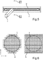
- FIG. 6 left shows the irradiation of a reduced area with variable filter pendulum speed and jet speed.
- t 1 and t 2 represent different irradiation times of the beam lines.
- Reference numeral 34 denotes the variable pendulum movement of the filter unit 6 and the ion beam 2.
- the ion beam 2 is only deflected in the z direction to such an extent that the ion beam 2 essentially only hits the wafer 8.
- the end points of the deflection of the ion beam 2 in the z direction are here adapted to the dimensions of the wafer 8.
- the filter 6 moves step by step in the y-direction. According to a further example it is provided that the filter 6 moves continuously in the y-direction.
- the speed of the slow pendulum movement of the ion beam 2 and the energy filter 6 in the y-direction is adapted to the time it takes for the ion beam 2 to sweep over the wafer in the z-direction once or several times in order to ensure that the To ensure ion beam 2 and the energy filter 6, ie to ensure that the ion beam 2 always hits the wafer through the filter 6.
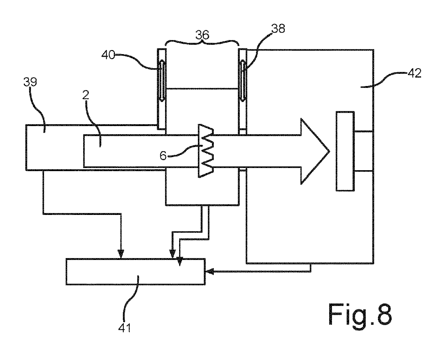
- the main idea here is to place the devices that are required for installing the energy filter chip in the irradiation system in one facing the wafer chamber 42 (which are also referred to as a wafer end station, wafer handling chamber or implantation chamber can) separate, vacuum-technically lockable unit (which can also be referred to as filter chamber 36) to be arranged, as shown, for example, in Fig. 8 is shown.
- the wafer chamber 42 which are also referred to as a wafer end station, wafer handling chamber or implantation chamber can
- separate, vacuum-technically lockable unit which can also be referred to as filter chamber 36
- the filter chamber 36 has two openings, which are opened by closures or valves (first vacuum valve 38 and second vacuum valve 40 in Fig. 8 ) can be closed. These closures are opened in the irradiation mode and are arranged in such a way that when the closures are open, the ion beam 2 coming from the accelerator can pass unhindered through the filter 6 onto the substrate 8 to be irradiated. If the openings are closed, the filter 6 in the filter chamber 36 is protected from external mechanical influences. According to one example, the openings can be closed in a pressure-tight manner by the closures, so that after closing the same pressure conditions are maintained that prevailed in the filter chamber 36 before closing. A vacuum pump 41 can be connected to the filter chamber 36, which, when the openings are closed, can compensate for pressure fluctuations which can result, for example, from non-hermetically sealed closures.
- the openings are closed prior to venting.
- the separate filter chamber 36 continues to be pumped, so that the particle load on the filter 6 is minimized and the pressure conditions remain constant. Mechanical loading of the filter 6 due to pumping or ventilation processes are avoided in this way.
- the separate energy filter vacuum chamber 36 is closed during wafer delivery and open during implantation. It is separated from the wafer chamber 42 by means of at least one vacuum valve 38.
- the wafer chamber 42 is designed as a "commercial" wafer chamber 42 according to the prior art. During the ion implantation, high vacuum or ultra-high vacuum conditions are present in it.
- the filter 6 is attached according to the prior art and / or according to flexible mounting options. A common vacuum pump system or several independent vacuum pump systems 41 can be present.
- the energy filter 6 is arranged in the upstream separate vacuum unit (filter chamber 36) on a movable device (filter holder 44).
- This device 44 serves to bring the energy filter 6 closer to the substrate 8 to be irradiated, possibly due to the design of the separate vacuum unit 36 and the wafer chuck 45 between substrate 8 and filter 6.
- the filter 6 can (but does not have to) also pass through one of the open closures or vacuum valves (vacuum valve 38 in Fig. 9 ) are moved through. In front Closing the filter chamber 36, for example when changing a wafer, the filter 6 is then moved back into the filter chamber 36.
- the energy filter holder 44 is mechanically transferred to the wafer end station 42 in order to adjust the distance between wafer 8 and filter 6.
- the double arrow indicates the forward / backward movable energy filter installation. Otherwise, the reference symbols denote the same elements with the same properties as in FIG Fig. 8 .
- the filter chamber 36 is arranged outside the wafer chamber 42 in front of the beam opening (implantation opening) of the wafer chamber 42.
- the beam opening is the opening through which the ion beam 2 enters the wafer chamber 42.
- the above-described separate vacuum-technical unit (filter chamber 36) for receiving the energy filter chip is arranged within the wafer chamber 42 (end station). In this case, too, the mechanical movement of the filter 6 in the direction of the substrate 8 may be necessary. Otherwise, the reference symbols denote the same elements with the same properties as in FIG Fig. 8 .
- the axis labels PDC designate the point defect concentration, IIC the implanted ion concentration and d the depth.
- Reference number 46 denotes the implanted ion concentration
- reference number 48 denotes the left axis
- reference number 50 denotes the right axis
- reference number 52 denotes the cold implantation defect concentration
- reference number 54 denotes the hot implantation defect concentration
- reference number 56 denotes non-end-of-range defects
- Reference numeral 58 denotes end-of-range defects 58 and the two downwardly directed parallel arrows in FIG Figures 12-14 indicate the reduced defect concentration.
- point defects are formed due to collisions of the injected ions with atoms of the substrate material. With unfiltered implantations, these point defects reach a concentration maximum in the end-of-range area of the injected foreign atoms.
- the use of an energy filter 6 in combination with a heatable wafer chuck 45 is proposed, see Fig. 11 .
- the “wafer chuck” 45 is a receptacle for the wafer 8 in the wafer chamber 42 and holds the wafer 8 during the implantation.
- a heatable wafer holder wafer chuck 45, wafer wheel 20 or any other holder
- an energy filter 6 for ion implantation can be Generate unknown combinations of point defect and foreign atom profiles.
- a heatable wafer holder 45 is suitable for wafers 8 made of SiC, but also for wafers 8 made of any other semiconductor materials.
- the energy filter 6 can be in any kind of arrangement, such as static, movable, in a separate chamber, in the same chamber as the wafer chuck 45, smaller than the wafer 8, larger than or the same size as the wafer 8, rotating, with a collimation structure, etc.
- the stress on the novel defect profiles extends to all implantation profiles and their associated defect profiles and for all cases of defect accumulation or ion beam-induced healing, i.e. in particular for the two cases “case 1" and "case 2".
- the wafer 8 is preferably a semiconductor wafer.
- other wafers for example made of optical materials such as LiNbO3, can also be processed.
- an energy filter was usually mentioned as an implantation filter 6 as an example.
- other implantation filters known from the prior art can also be used within the scope of the invention.
- Wafer chuck 45 and wafer wheel 20 were named as wafer receptacles in the context of the description. However, all other conventional wafer holders can also be used.
Landscapes
- Chemical & Material Sciences (AREA)
- Analytical Chemistry (AREA)
- Engineering & Computer Science (AREA)
- Chemical Kinetics & Catalysis (AREA)
- Materials Engineering (AREA)
- Mechanical Engineering (AREA)
- Metallurgy (AREA)
- Organic Chemistry (AREA)
- Inorganic Chemistry (AREA)
- Physical Vapour Deposition (AREA)
- Physics & Mathematics (AREA)
- Condensed Matter Physics & Semiconductors (AREA)
- General Physics & Mathematics (AREA)
- Manufacturing & Machinery (AREA)
- Computer Hardware Design (AREA)
- Microelectronics & Electronic Packaging (AREA)
- Power Engineering (AREA)
- Crystallography & Structural Chemistry (AREA)
- Container, Conveyance, Adherence, Positioning, Of Wafer (AREA)
Abstract
Beschrieben wird eine Vorrichtung mit einer Waferkammer (42), die eine Waferaufnahme (20, 45) aufweist, die dazu ausgebildet ist, wenigstens einen Wafer (8) aufzunehmen, und mit einer Filterkammer (36), die eine Filterhalterung (44) und eine erste und zweite verschließbare Öffnung aufweist.
Description
Die Erfindung betrifft ein Verfahren und eine Vorrichtung zur Ionenimplantation in Wafern.The invention relates to a method and a device for ion implantation in wafers.
Konkreter beschäftigt sich die Erfindung mit apparativen Aspekten der Dotierung von Halbleitern bzw. der Erzeugung von Defektprofilen zur Modifikation der Ladungsträgerlebensdauer in Halbleiterbauelementen mittels Einsatz eines Energiefilters für Ionenimplantation.More specifically, the invention deals with apparatus-related aspects of doping semiconductors or the generation of defect profiles to modify the charge carrier life in semiconductor components by using an energy filter for ion implantation.
Hierzu existieren beispielsweise folgende Referenzen:
- [1]
ICSCRM2015: "Alternative highly homogenous drift layer doping for 650 V SiC devices" R. Rupp, W. Schustereder, Tobias Höchbauer, Ronny Kern, Michael Rüb, Constantin Casato, Florian Krippendorf - [2] "
Energy filter for tailoring depth profiles in semiconductor doping application" - Constantin Csato, Florian Krippendorf, Shavkat Akhmadaliev, Johannes von Borany, Weiqi Han, Thomas Siefke, Andre Zowalla, Michael Rüb, Nucl. Instr. Meth. B (2015), http://dx.doi.org/10.1016/j.nimb.2015.07.102 - [3] "
Analysis of lateral energy distribution for passive ion beam scattering element" - Weiqi Han, Constantin Csato, Florian Krippendorf, Michael Rüb, Carsten Ronning, DPG Frühjahrstagung Dresden, März 2014 - [4] "
Investigation of dopant profiles, losses and heating using an energy filter for ion implantation" - Krippendorf, Csato, Rüb, DPG Frühjahrstagung Dresden, März 2014
"The Gap Between Research and Commercial Product in Applied Physics Research - An Issue for Sustainability and an Opportunity?" - Prof. Dr. Michael Rueb, University of Applied Sciences Jena, 6th ICEBE International Conference on Engineering and Business Education, Windhoek, Namibia, 7.-10. Oktober 2013 - [5] "Energiefilter für Ionenimplantation" -
F. Krippendorf, C. Csato, T. Bischof, S. Gupta, W. Han, M. Nobst, Ernst-Abbe-Fachhochschule Jena; C. Ronning, Friedrich-Schiller-Universität Jena; R. Rupp, Infineon Technologies AG, Neubiberg; A. Schewior, Ernst-Abbe-Fachhochschule Jena; W. Wesch, Friedrich-Schiller-Universität Jena; W. Morgenroth, Institut für Photonische Technologien e.V., Jena; M. Rüb, Ernst-Abbe-Fachhochschule Jena, Mikrosystemtechnik Kongress, Aachen, Oktober 2014, "Energiefilter für Ionenimplantationsanlagen Idee- erste Experimente - Anwendung, C - [6]
Csato, T. Bischof, S. Gupta, W. Han, F. Krippendorf, W.Morgenroth, M. Nobst, C. Ronning, R. Rupp, A. Schewior, W. Wesch, M. Rüb, 12. Juni 2013, Workshop "Ionenstrahlen - Forschung und Anwendung" 2013, Leibniz-Institut für Oberflächenmodifizierung Leipzig, M. Rüb, T. Bischof, C. Csato, S. Gupta, W. Han, F. Krippendorf, A. Schewior, C. Möse, "Energiefilter für Ionenimplantationsanlagen", Forschungsbericht der Ernst-Abbe-Fachhochschule Jena 2011/2012 - [7]
EP 0 014 516 A1 - [8]
Rüb, "Energiefilter für Hochenergieionenimplantation", IP.com Offenlegungsnummer: IPCOM000018006D, ursprüngliches Veröffentlichungsdatum: 1. Dezember 2001, aufgenommen in der Datenbank zum Stand der Technik: 23. Juli 2003 bzw. Siemens AG, 2001, Siemens Technik Report, Dez. 2001, 9 Seit - [9]
DE 10 2011 075350 A1
- [1]
ICSCRM2015: "Alternative highly homogeneous drift layer doping for 650 V SiC devices" R. Rupp, W. Schustereder, Tobias Höchbauer, Ronny Kern, Michael Rüb, Constantin Casato, Florian Krippendorf - [2] "
Energy filter for tailoring depth profiles in semiconductor doping application "- Constantin Csato, Florian Krippendorf, Shavkat Akhmadaliev, Johannes von Borany, Weiqi Han, Thomas Siefke, Andre Zowalla, Michael Rüb, Nucl. Instr. Meth. B (2015), http: //dx.doi.org/10.1016/j.nimb.2015.07.102 - [3] "
Analysis of lateral energy distribution for passive ion beam scattering element "- Weiqi Han, Constantin Csato, Florian Krippendorf, Michael Rüb, Carsten Ronning, DPG Spring Conference Dresden, March 2014 - [4] "
Investigation of dopant profiles, losses and heating using an energy filter for ion implantation "- Krippendorf, Csato, Rüb, DPG Spring Conference Dresden, March 2014
"The Gap Between Research and Commercial Product in Applied Physics Research - An Issue for Sustainability and an Opportunity? "- Prof. Dr. Michael Rueb, University of Applied Sciences Jena, 6th ICEBE International Conference on Engineering and Business Education, Windhoek, Namibia, 7 .-October 10th, 2013 - [5] "Energy filter for ion implantation" -
F. Krippendorf, C. Csato, T. Bischof, S. Gupta, W. Han, M. Nobst, Ernst Abbe University of Applied Sciences Jena; C. Ronning, Friedrich Schiller University Jena; R. Rupp, Infineon Technologies AG, Neubiberg; A. Schewior, Ernst Abbe University of Applied Sciences Jena; W. Wesch, Friedrich Schiller University Jena; W. Morgenroth, Institute for Photonic Technologies eV, Jena; M. Rüb, Ernst Abbe University of Applied Sciences Jena, microsystem technology Congress, Aachen, October 2014, "Energy filters for ion implantation systems Idea - first experiments - application, C - [6]
Csato, T. Bischof, S. Gupta, W. Han, F. Krippendorf, W.Morgenroth, M. Nobst, C. Ronning, R. Rupp, A. Schewior, W. Wesch, M. Rüb, June 12, 2013 , Workshop "Ion Beams - Research and Application" 2013, Leibniz Institute for Surface Modification Leipzig, M. Rüb, T. Bischof, C. Csato, S. Gupta, W. Han, F. Krippendorf, A. Schewior, C. Möse, "Energy filters for ion implantation systems", research report from the Ernst Abbe University of Applied Sciences Jena 2011/2012 - [7]
EP 0 014 516 A1 - [8th]
Rüb, "Energy filter for high-energy ion implantation", IP.com disclosure number: IPCOM000018006D, original publication date: December 1, 2001, included in the database on the state of the art: July 23, 2003 or Siemens AG, 2001, Siemens Technik Report, December 2001 , 9 p - [9]
DE 10 2011 075350 A1
In der mikrotechnischen kommerziell ausgerichteten Produktion werden mittels Ionenimplantation die Dotierung bzw. die Erzeugung von Defektprofilen in beliebigen Materialien, wie etwa Halbleitern (Silizium, Siliziumcarbid, Galliumnitrid) oder optischen Materialien (LiNbO3), mit vordefinierten Tiefenprofilen im Tiefenbereich von wenigen Nanometern bis hin zu einigen 100 Mikrometern realisiert.In microtechnical, commercially oriented production, ion implantation is used to doping or generating defect profiles in any materials, such as semiconductors (silicon, silicon carbide, gallium nitride) or optical materials (LiNbO3), with predefined depth profiles ranging from a few nanometers to a few 100 micrometers realized.
Hierzu eignet sich ein sogenanntes Energiefilter 6 für Ionenimplantation. Ein solches Energiefilter 6 ist beispielsweise in
Das Energiefilter 6 ist derart strukturiert, dass es unterschiedlich dicke Bereiche besitzt. Der dickste Bereich ist beispielsweise mehr als 1,5-mal, mehr als 2-mal, mehr als 3-mal oder mehr als 5-mal so dick wie der dünnste Bereich. Die Struktur kann beispielsweise dreieckförmig sein, wie in
Das Grundprinzip des Energiefilters 6 ist wie folgt: Ein monoenergetischer lonenstrahl 2 wird beim Durchtritt durch die mikrostrukturierte Energiefilterkomponente abhängig vom Eintrittsort in seiner Energie modifiziert. Die resultierende Energieverteilung der Ionen führt zu einer Modifikation des Tiefenprofils des implantierten Stoffes in der Matrix des Substrats 8.The basic principle of the
In
Energiefilteraufhängung 16 und Waferrad 20 sind im Beispiel der
Schließlich wurde gezeigt, dass die Erhöhung der Substrattemperatur, insbesondere bei Verwendung von SiC, zu einer Reduktion der Punktdefektkonzentration führt. Dies ist insbesondere bei Hochdosisimplantationen von AI in SiC beobachtet worden. Siehe hierzu
Die vorliegende Erfindung liefert Lösungen für folgende Problemstellungen:The present invention provides solutions to the following problems:
Es ist wünschenswert, auf die mechanisch aufwändige Rotations- und Pendelbewegung des Waferrades 20 verzichten zu können.It is desirable to be able to dispense with the mechanically complex rotating and pendulum movement of the
Wird das Energiefilter 6 in einer Öffnung der Implantationskammer 13 (die auch als Bestrahlungskammer oder Waferkammer bezeichnet werden kann) positioniert, wie dies in
Es ist wünschenswert, dass während der Implantation möglichst wenige Punktdefekte im Halbleitermaterial erzeugt werden. Bekannte Defektprofile für eine Kettenimplantation mit mehreren diskreten Implantationsenergien sind in
Es sind zwei Fälle unterschieden. Fall 1 (
Bei der Lösung der oben genannten Problemstellungen sollten insbesondere folgende Nebenbedingungen beachtet werden:
- (A) Der
Abstand zwischen Energiefilter 6 und Substrat 8 (Wafer) bei der Implantation sollte zwischen einigen Millimetern und wenigen Zentimetern betragen. - (B)
Das Energiefilter 6 sollte in seinen lateralen Abmessungen möglichst groß sein, um den Energieeintragdurch den lonenstrahl 2 auf eine möglichst große Fläche zu verteilen. Dadurch wird die Aufheizung desEnergiefilters 6 verringert und die Stromtragfähigkeit erhöht. - (C) Die Aufnahme des
Energiefilters 6 sollte möglichst flexibel zu gestalten sein, da nach heutigem Entwicklungsstand zu erwarten ist, dass für unterschiedliche Applikationen unterschiedliche Konzepte der Energiefilterausgestaltung benötigt werden. - (D)
Die Filtermembran 18 sollte möglichst keinen mechanischen Vibrationen ausgesetzt sein, wie sie etwa bei Belüftungs- und Abpumpvorgängen während des Wechsels der zu bestrahlendenSubstrate 8 auftreten können. - (E)
Die mikrostrukturierte Filtermembran 18 sollte möglichst nicht der partikelbehafteten Außenluft ausgesetzt sein, da bei Ablagerung von Partikeln ggfs. die Funktionalität desEnergiefilters 6 eingeschränkt sein könnte. - (F) Die Vorrichtung zur Anordnung des
Energiefilters 6 und des Waferchucks 45oder Waferrads 20 sollte so gestaltet sein, dass durch Anwendung desEnergiefilters 6 Implantationsprofile derart erzeugt werden, dass die Generation von Punktdefekten, insbesondere im Fall des Halbleitermaterials SiC, reduziert sein soll.
- (A) The distance between
energy filter 6 and substrate 8 (wafer) during implantation should be between a few millimeters and a few centimeters. - (B) The
energy filter 6 should be as large as possible in terms of its lateral dimensions in order to distribute the energy input by theion beam 2 over the largest possible area. This reduces the heating of theenergy filter 6 and increases the current-carrying capacity. - (C) The inclusion of the
energy filter 6 should be designed to be as flexible as possible, since according to the current state of development it is to be expected that different concepts of the energy filter design are required for different applications. - (D) The
filter membrane 18 should as far as possible not be exposed to mechanical vibrations, such as can occur during ventilation and pumping processes during the change of thesubstrates 8 to be irradiated. - (E) The
microstructured filter membrane 18 should as far as possible not be exposed to the outside air containing particles, since the functionality of theenergy filter 6 could possibly be restricted if particles are deposited. - (F) The device for arranging the
energy filter 6 and thewafer chuck 45 orwafer wheel 20 should be designed in such a way that, by using theenergy filter 6, implantation profiles are generated in such a way that the generation of point defects, in particular in the case of the semiconductor material SiC, is to be reduced.
Erfindungsgemäße Lösungen sind in den unabhängigen Ansprüchen definiert und werden nachfolgend unter Bezugnahme auf die Zeichnungen näher beschrieben. Beschrieben werden insbesondere mögliche Ausgestaltungen einer Ionenimplantationsanlage oder von Teilen einer solchen Ionenimplantationsanlage und Verfahren zum Betreiben einer Ionenimplantationsanlage und von deren Teilen. Diese Anlagen und Verfahren eignen sich für die Implantation von Ionen in Wafer aus einem beliebigen Halbleitermaterial, insbesondere jedoch für Wafer auf Basis von Siliziumkarbid (SiC).
-
Fig. 1 zeigt dasGrundprinzip eines Energiefilters 6 bei der Ionenimplantation; -
Fig. 2a ist eine Darstellung einer Implantationskammer 13 nach dem Stand der Technik; -
Fig. 2b ist eine Darstellung eines Strahllinien-Einsatzes 14mit Filtermembran 18 nach dem Stand der Technik; -
Fig. 3a und 3b zeigen bekannte Punktdefektkonzentrationsprofile in SiC für diskrete Kettenimplantationen; -
Fig. 4 ist eine Querschnittsansicht eines lonenimplantations-Setups mit fixiertem Substrat, gescanntem lonenstrahl sowie implementiertem Energiefilter mit synchronisierter Pendelbewegung zwischen lonenstrahl und Energiefilter in y-Richtung; -
Fig. 5 ist eine Darstellung einer angepassten Ionenstrahlablenkung zur Bestrahlung der aktiven Fläche des Energiefilters; -
Fig. 6 zeigt eine schematische Darstellung der Bestrahlung eines Substrates mit i) (Fig. 6 rechts) konstanter Strahl-Pendelgeschwindigkeit in y und z und konstanter Energiefilter-Pendelbewegung in y bei konstantem lonenstrom und ii) (Fig. 6 links) reduzierter Bestrahlungsfläche durch variable Filter-Pendelbewegung in y und variabler Ionenstrahlbewegung in y und z bei konstantem lonenstrom; -
Fig. 7 zeigt eine schematische Darstellung der Bestrahlung reduzierter Fläche mit variabler Pendelbewegung des Energiefilters; -
Fig. 8 zeigt eine separate Filterkammer, die der eigentlichen Waferkammer vorgelagert ist; -
Fig. 9 zeigt eine separate Filterkammer, die der eigentlichen Waferkammer vorgelagert ist, wobei die Vorrichtung zur Halterung des Energiefilters so angeordnet ist, dass sie, bezogen auf den Waferchuck, vorwärts oder rückwärts in die Nähe des Waferchucks gefahren werden kann; -
Fig. 10 zeigt eine separate Filterkammer, die innerhalb der Waferkammer angeordnet ist; -
Fig. 11 zeigt eine Energiefilteranordnung in Kombination mit einer heizbaren Waferaufnahmeeinrichtung; -
Fig. 12 zeigt ein neuartiges Defekt- und Fremdatomprofil (Fall 1); -
Fig. 13 zeigt ein neuartiges Defekt- und Fremdatomprofil (Fall 2); und -
Fig. 14 zeigt ein neuartiges Defekt- und Fremdatomprofil, genauer ein von der Oberfläche isoliertes Dotierprofil.
-
Fig. 1 shows the basic principle of anenergy filter 6 in ion implantation; -
Fig. 2a Fig. 3 is an illustration of a priorart implantation chamber 13; -
Figure 2b Figure 3 is an illustration of a prior artjet line insert 14 withfilter membrane 18; -
Figures 3a and 3b show known point defect concentration profiles in SiC for discrete chain implants; -
Fig. 4 is a cross-sectional view of an ion implantation setup with a fixed substrate, scanned ion beam and implemented energy filter with synchronized pendulum movement between ion beam and energy filter in the y-direction; -
Fig. 5 is an illustration of an adapted ion beam deflection for irradiating the active surface of the energy filter; -
Fig. 6 shows a schematic representation of the irradiation of a substrate with i) (Fig. 6 right) constant beam pendulum speed in y and z and constant energy filter pendulum motion in y with constant ion current and ii) (Fig. 6 left) reduced irradiation area due to variable filter pendulum movement in y and variable ion beam movement in y and z with constant ion current; -
Fig. 7 shows a schematic representation of the irradiation of a reduced area with a variable pendulum movement of the energy filter; -
Fig. 8 shows a separate filter chamber upstream of the actual wafer chamber; -
Fig. 9 shows a separate filter chamber in front of the actual wafer chamber, the device for holding the energy filter being arranged so that it can be moved forwards or backwards in relation to the wafer chuck in the vicinity of the wafer chuck; -
Fig. 10 Figure 12 shows a separate filter chamber located within the wafer chamber; -
Fig. 11 shows an energy filter arrangement in combination with a heatable wafer receiving device; -
Fig. 12 shows a novel defect and foreign atom profile (case 1); -
Fig. 13 shows a novel defect and foreign atom profile (case 2); and -
Fig. 14 shows a new type of defect and foreign atom profile, more precisely a doping profile isolated from the surface.
Im Folgenden wird eine erste Ausführungsform der Erfindung näher beschrieben. Für eine homogene Bestrahlung eines Wafers 8 (Substrat) sollte der durch das Implantationsfilter 6 geleitete lonenstrahl 2 während der Implantation die gesamte Waferfläche (Substratfläche) überstreichen (scannen). Hierzu ist eine elektrostatische Ablenkung (Scanning) des lonenstrahls 2 in Kombination mit einer mechanischen Bewegung des Filters 6 vorgesehen. Ein möglicher Aufbau ist in den
Das Scanning erfolgt in y- und z-Richtung elektrostatisch, jedoch für jede Richtung auf unterschiedliche Art und Weise. In z-Richtung erfolgt ein schnelles Scanning, sodass das schlitzartige Energiefilter 6 über die gesamte aktive Fläche bestrahlt wird. Das Scanning in y-Richtung geschieht durch eine langsame elektrostatische Pendelbewegung, welche synchron mit einer gekoppelten mechanischen Pendelbewegung des Filters 6 ausgeführt wird. Somit weisen der Ionenstrahl 2 und die aktive Fläche des Energiefilters 6 stets Deckungsgleichheit auf, so dass der lonenstrahl 2 stets durch das Filter 6 geleitet wird, bevor er auf den Wafer 8 trifft. In der z-Richtung kann eine Abmessung des Filters 6 der maximalen Abmessung des Wafers 8 in der z-Richtung entsprechen, so dass in der z-Richtung keine mechanische Bewegung des Filters 6 erforderlich ist und nur der lonenstrahl 2 in dieser z-Richtung bewegt wird. In der y-Richtung ist die Abmessung des Filters 6 kleiner als die maximale Abmessung des Wafers 8, so dass in dieser Richtung das Filter 6 synchron mit dem lonenstrahl 2 bewegt wird, um während der Implantation sukzessive alle Bereiche des Wafers 8 mit dem durch das Filter 6 geleiteten Ionenstrahl 2 zu bestrahlen.The scanning is carried out electrostatically in the y and z directions, but in a different way for each direction. Fast scanning takes place in the z-direction, so that the slit-
Eine weitere Abwandlung der oben beschriebenen Ausführungsform ist im Folgenden dargelegt:
Für eine Durchsatzoptimierung des Energiefilters 6 kann es wünschenswert sein, die bestrahlte Fläche neben dem Wafer 8 (Overscan) möglichst klein zu halten, d.h. möglichst nur den runden Wafer 8, nicht jedoch den Wafer 8 umgebende Bereiche zu bestrahlen. Im einfachsten Fall der Bestrahlung nach
To optimize the throughput of the
Bei einem runden Wafer 8 werden dadurch auch Flächen bestrahlt, die innerhalb des rechteckigen Bestrahlungsbereichs, aber außerhalb des Wafers 8 liegen. Dies ist anhand von
Eine Substrat-optimierte Ablenkung des lonenstrahls 2 in z-Richtung ist in
Gemäß
Gemäß einem Beispiel ist vorgesehen, dass sich das Filter 6 in der y-Richtung schrittweise bewegt. Gemäß einem weiteren Beispiel ist vorgesehen, dass sich das Filter 6 in der y-Richtung kontinuierlich bewegt. In diesem Fall wird die Geschwindigkeit der langsamen Pendelbewegung des Ionenstrahles 2 und des Energiefilters 6 in der y-Richtung an die Zeit angepasst, die der lonenstrahl 2 benötigt, um den Wafer in der z-Richtung einmal oder mehrmals zu überstreichen, um stets Deckungsgleichheit des Ionenstrahls 2 und des Energiefilters 6 zu gewährleisten, d.h. um zu gewährleisten, dass der Ionenstrahl 2 stets durch das Filter 6 auf den Wafer trifft.According to one example it is provided that the
Im Folgenden werden weitere Ausführungsformen der Erfindung beschrieben.Further embodiments of the invention are described below.
Der wesentliche Gedanke besteht dabei darin, die Vorrichtungen, die für den Einbau des Energiefilterchips in die Bestrahlungsanlage benötigt werden, in einer zur Waferkammer 42 (die auch als Waferendstation, Waferhandlingskammer oder Implantationskammer bezeichnet werden kann) separaten, vakuumtechnisch abschließbaren Einheit (die auch als Filterkammer 36 bezeichnet werden kann) anzuordnen, wie dies beispielsweise in
Die Filterkammer 36 weist zwei Öffnungen auf, die durch Verschlüsse bzw. Ventile (erstes Vakuumventil 38 und zweites Vakuumventil 40 in
Wenn die Waferkammer 42 z.B. zum Substratwechsel belüftet werden muss, werden vor der Belüftung die Öffnungen geschlossen. Die separate Filterkammer 36 wird weiterhin bepumpt, so dass die Partikelbelastung des Filters 6 minimiert wird und die Druckverhältnisse konstant bleiben. Mechanische Belastung des Filters 6 durch Abpump- oder Belüftungsvorgänge werden auf diese Weise vermieden.If the
Die separate Energiefilter-Vakuumkammer 36 ist geschlossen während der Waferzuführung und offen während der Implantation. Sie ist getrennt von der Waferkammer 42 mittels wenigstens eines Vakuumventils 38. Die Waferkammer 42 ist als "kommerzielle" Waferkammer 42 nach dem Stand der Technik ausgebildet. Während der Ionenimplantation liegen in ihr Hochvakuum- oder Ultrahochvakuumbedingungen vor. Der Filter 6 ist befestigt gemäß dem Stand der Technik und/oder gemäß flexiblen Halterungsoptionen. Es können ein gemeinsames oder mehrere unabhängige Vakuumpumpsysteme 41 vorliegen.The separate energy
In einer weiteren Ausführungsform, siehe
Bei den in
Weitere Ausführungsformen der Erfindung werden im Folgenden unter Bezugnahme auf
Während jeder Ionenimplantation kommt es aufgrund von Kollisionen der eingeschossenen Ionen mit Atomen des Substratmaterials zur Bildung von Punktdefekten. Diese Punktdefekte erreichen bei ungefilterten Implantationen im End-of-Range-Bereich der eingeschossenen Fremdatome ein Konzentrationsmaximum.During each ion implantation, point defects are formed due to collisions of the injected ions with atoms of the substrate material. With unfiltered implantations, these point defects reach a concentration maximum in the end-of-range area of the injected foreign atoms.
Vorgeschlagen wird der Einsatz eines Energiefilters 6 in Kombination mit einem beheizbaren Waferchuck 45, siehe
Das Energiefilter 6 kann in jeder Art von Anordnung vorliegen, wie z.B. statisch, bewegbar, in separater Kammer, in derselben Kammerwie der Waferchuck 45, kleiner als der Wafer 8, größer als oder gleich groß wie der Wafer 8, rotierend, mit Kollimationsstruktur etc.The
Profilkombinationen, die sich durch Bestrahlen eines Wafers 8 über ein Energiefilter 6 erreichen lassen, haben beispielsweise folgende Eigenschaften:
- Die Punktdefektkonzentration (PDC) ist im gesamten durch
das Energiefilter 6 aufgeweiteten Tiefenbereich der Implantation reduziert. - Der aufgeweitete Tiefenbereich reicht typischerweise von der Oberfläche bis zu einigen Mikrometern Tiefe, siehe
Fig. 12 und 13 . - Die Konzentrationstiefenfunktion der implantierten Fremdatome ist abhängig von der geometrischen und materialtechnischen Ausgestaltung des
Energiefilters 6 und somit vollständig beinflussbar. Die Defekttiefenprofile folgen der Form der Konzentrationstiefenfunktion der implantierten Fremdatome und sind für ein gegebenes Substratmaterial durch sie bestimmt, sieheFig. 12 und 13 . - Die Defektkonzentrationstiefenprofile sind auch davon abhängig, ob es durch den Ionenbeschuss in tieferliegenden Gebieten zu ionenstrahlinduzierten Ausheileffekten ("
Fall 1") kommt. Somit sind die Fälle "Fall 1" (Fig. 12 ) und "Fall 2" (Fig. 13 und 14 ) zu unterscheiden. "Fall 1" umfasst ausdrücklich auch den Fall, dass die ionenstrahlinduzierte Ausheilung sehr effizient ist und es somit (bei boxförmigem Fremdatomprofil) zu einem Anstieg der Defektkonzentration mit der Tiefe kommt. - Die Fremdatom- und Punktdefekttiefenprofile sind glatt, d.h. sie sind nicht durch peakartige Konzentrationsmaxima und -minima entlang der Tiefe charakterisiert. Es resultiert keine "Welligkeit" des Defektprofils.
- Der aufgeweitete Tiefenbereich kann auch unterhalb der Oberfläche beginnen und sich z.B. beginnend ab 2µm Tiefe bis in eine Tiefe von 6µm erstrecken, siehe
Fig. 14 . In diesem Fall ist zu unterscheiden zwischen End-of-Range-Defekten 58 und Nicht-End-of-Range-Defekten 56. Für beide Defektarten gilt, dass eine Reduktion der Konzentration durch die erhöhte Temperatur bei der Implantation erreicht wird. - In einer weiteren Ausführungsform liegt der Tiefenbereich bei < 1µm.
- Das implantierte Ion ist beispielsweise Aluminium mit hohen Konzentrationen.
- Erhöhter Aktivierungsgrad und reproduzierbare Aktivierung im Vergleich zur Niedertemperatur-Energiefilterimplantation
- Die Temperatur des Waferchucks 45 ist ab Raumtemperatur nach oben einstellbar und liegt bevorzugt zwischen T=400°C und T=1.000°C.
- The point defect concentration (PDC) is reduced in the entire depth range of the implantation expanded by the
energy filter 6. - The expanded depth range typically extends from the surface to a few micrometers in depth, see
Fig. 12 and13th . - The depth of concentration function of the implanted foreign atoms is dependent on the geometric and material design of the
energy filter 6 and can therefore be completely influenced. The defect depth profiles follow the shape of the concentration depth function of the implanted foreign atoms and are determined by them for a given substrate material, seeFig. 12 and13th . - The defect concentration depth profiles also depend on whether the ion bombardment leads to ion beam-induced healing effects ("
case 1") in deeper regions. Thus the cases "Case 1" (Fig. 12 ) and "Case 2" (Figures 13 and 14 ) to distinguish. "Case 1" also expressly includes the case that the ion beam-induced healing is very efficient and thus (with a box-shaped foreign atom profile) the defect concentration increases with depth. - The foreign atom and point defect depth profiles are smooth, ie they are not characterized by peak-like concentration maxima and minima along the depth. There is no "waviness" of the defect profile.
- The expanded depth range can also begin below the surface and extend, for example, starting from a depth of 2 μm to a depth of 6 μm, see FIG
Fig. 14 . In this case, a distinction must be made between end-of-range defects 58 and non-end-of-range defects 56. For both types of defects, the concentration is reduced by the increased temperature during implantation. - In a further embodiment, the depth range is <1 μm.
- The implanted ion is, for example, aluminum with high concentrations.
- Increased degree of activation and reproducible activation compared to low-temperature energy filter implantation
- The temperature of the
wafer chuck 45 can be adjusted upwards from room temperature and is preferably between T = 400 ° C and T = 1,000 ° C.
Die Beanspruchung der neuartigen Defektprofile (bei erhöhter Implantationstemperatur) erstreckt sich auf alle durch Energiefilteranwendung darstellbaren Implantationsprofile und deren dazugehörigen Defektprofile und für alle Fälle von Defektakkumulation oder ionenstrahlinduziertes Ausheilen, d.h. insbesondere für die beiden Fälle "Fall 1" und "Fall 2".The stress on the novel defect profiles (with increased implantation temperature) extends to all implantation profiles and their associated defect profiles and for all cases of defect accumulation or ion beam-induced healing, i.e. in particular for the two cases "
Der Wafer 8 ist vorzugsweise ein Halbleiterwafer. Es können aber auch andere Wafer, beispielsweise aus optischen Materialien wie LiNbO3, bearbeitet werden.The
In den beschriebenen Ausführungsformen wurde als Implantationsfilter 6 meist beispielhaft ein Energiefilter genannt. Es können aber auch andere aus dem Stand der Technik bekannte Implantationsfilter im Rahmen der Erfindung verwendet werden.In the described embodiments, an energy filter was usually mentioned as an
Als Waferaufnahme wurden im Rahmen der Beschreibung beispielhaft Waferchuck 45 und Waferrad 20 genannt. Es können aber auch alle anderen herkömmlichen Waferaufnahmen verwendet werden.
- 22
- lonenstrahlion beam
- 33
- erstes Ionfirst ion
- 44th
- zweites Ionsecond ion
- 66th
- ImplantationsfilterImplantation filter
- 88th
- WaferWafer
- 1010
- Rechteck (mit Filter)Rectangle (with filter)
- 1212th
- Gaußverteilung (ohne Filter)Gaussian distribution (without filter)
- 1313th
- ImplantationskammerImplantation chamber
- 1414th
- Strahllinien-EinsatzBeamline insert
- 1515th
- StrahlöffnungBeam opening
- 1616
- Aufhängungsuspension
- 1818th
- FiltermembranFilter membrane
- 2020th
- WaferradWafer wheel
- 2222nd
- Welligkeit des DefektprofilsWaviness of the defect profile
- 2424
- Abnahme wegen SummationseffektenDecrease due to summation effects
- 2626th
- synchronisierte Pendelbewegung zwischen Energiefilter und lonenstrahl in y-Richtungsynchronized pendulum movement between energy filter and ion beam in y-direction
- 2828
- Pendelbewegung des lonenstrahls in z-RichtungPendulum motion of the ion beam in the z-direction
- 3232
- aktive Fläche des Energiefiltersactive surface of the energy filter
- 3434
- variable Pendelbewegung der Filtereinheit und des lonenstrahlsvariable pendulum movement of the filter unit and the ion beam
- 3636
- FilterkammerFilter chamber
- 3838
- erstes Vakuumventilfirst vacuum valve
- 3939
- VakuumzustandVacuum condition
- 4040
- zweites Vakuumventilsecond vacuum valve
- 4141
- VakuumpumpsystemVacuum pump system
- 4242
- WaferkammerWafer chamber
- 4444
- FilterhalterungFilter holder
- 4545
- WaferchuckWaferchuck
- 4646
- implantierte lonenkonzentrationimplanted ion concentration
- 4848
- linke Achseleft axis
- 5050
- rechte Achseright axis
- 5252
- Kaltimplantations-DefektkonzentrationCold implant defect concentration
- 5454
- Heißimplantations-DefektkonzentrationHot implant defect concentration
- 5656
- Nicht-End-of-Range-DefekteNon-end-of-range defects
- 5858
- End-of-Range-DefekteEnd-of-range defects
Claims (20)
Applications Claiming Priority (3)
| Application Number | Priority Date | Filing Date | Title |
|---|---|---|---|
| DE102016122791.9A DE102016122791B3 (en) | 2016-11-25 | 2016-11-25 | Ion implantation system, filter chamber and implantation method using an energy filter element |
| PCT/EP2017/080526 WO2018096145A1 (en) | 2016-11-25 | 2017-11-27 | Method and device for implanting ions in wafers |
| EP17804894.8A EP3545543A1 (en) | 2016-11-25 | 2017-11-27 | Method and device for implanting ions in wafers |
Related Parent Applications (1)
| Application Number | Title | Priority Date | Filing Date |
|---|---|---|---|
| EP17804894.8A Division EP3545543A1 (en) | 2016-11-25 | 2017-11-27 | Method and device for implanting ions in wafers |
Publications (4)
| Publication Number | Publication Date |
|---|---|
| EP3836188A2 true EP3836188A2 (en) | 2021-06-16 |
| EP3836188A3 EP3836188A3 (en) | 2021-11-03 |
| EP3836188B1 EP3836188B1 (en) | 2024-10-09 |
| EP3836188C0 EP3836188C0 (en) | 2024-10-09 |
Family
ID=60480316
Family Applications (2)
| Application Number | Title | Priority Date | Filing Date |
|---|---|---|---|
| EP17804894.8A Withdrawn EP3545543A1 (en) | 2016-11-25 | 2017-11-27 | Method and device for implanting ions in wafers |
| EP21154387.1A Active EP3836188B1 (en) | 2016-11-25 | 2017-11-27 | Method and device for ion implantation in wafers |
Family Applications Before (1)
| Application Number | Title | Priority Date | Filing Date |
|---|---|---|---|
| EP17804894.8A Withdrawn EP3545543A1 (en) | 2016-11-25 | 2017-11-27 | Method and device for implanting ions in wafers |
Country Status (6)
| Country | Link |
|---|---|
| US (3) | US11056309B2 (en) |
| EP (2) | EP3545543A1 (en) |
| JP (4) | JP6781895B2 (en) |
| CN (2) | CN110024075B (en) |
| DE (1) | DE102016122791B3 (en) |
| WO (1) | WO2018096145A1 (en) |
Families Citing this family (7)
| Publication number | Priority date | Publication date | Assignee | Title |
|---|---|---|---|---|
| DE102018114667B3 (en) | 2018-06-19 | 2019-09-19 | Infineon Technologies Ag | ION BEAM MODERATOR DEVICE, ION BEAM IMPLANT APPARATUS AND ION IMPLANTATION PROCESS |
| DE102019112773B4 (en) | 2019-05-15 | 2023-11-30 | mi2-factory GmbH | Device and method for implanting particles into a substrate |
| DE102019112985B4 (en) * | 2019-05-16 | 2024-07-18 | mi2-factory GmbH | Process for the production of semiconductor devices |
| LU101808B1 (en) * | 2020-05-15 | 2021-11-15 | Mi2 Factory Gmbh | An ion implantation device comprising energy filter and additional heating element |
| US20240047168A1 (en) * | 2020-12-17 | 2024-02-08 | mi2-factory GmbH | Energy Filter Assembly for Ion Implantation System with at least one coupling element |
| CN113163564B (en) * | 2021-04-30 | 2024-06-04 | 中国科学院电工研究所 | Electron beam processing device with static electricity eliminating function |
| CN116031126B (en) * | 2022-12-27 | 2025-09-23 | 北京烁科中科信电子装备有限公司 | A bunching resonance device for high energy ion implantation machine |
Citations (3)
| Publication number | Priority date | Publication date | Assignee | Title |
|---|---|---|---|---|
| EP0014516A1 (en) | 1979-01-04 | 1980-08-20 | Westinghouse Electric Corporation | Forming irradiated regions in semiconductor bodies by nuclear radiation |
| DE10239312B4 (en) | 2002-08-27 | 2006-08-17 | Infineon Technologies Ag | Method for producing a semiconductor component with a drift zone and a field stop zone and semiconductor component with a drift zone and a field stop zone |
| DE102011075350A1 (en) | 2011-05-05 | 2012-11-08 | Fachhochschule Jena | Energy filter assembly for ion implantation system used in fabrication of silicon wafer, has filter elements that are arranged in opening of energy filter which is vibrated vertical to propagation direction of ion beam |
Family Cites Families (27)
| Publication number | Priority date | Publication date | Assignee | Title |
|---|---|---|---|---|
| US4421988A (en) * | 1982-02-18 | 1983-12-20 | Varian Associates, Inc. | Beam scanning method and apparatus for ion implantation |
| JPS60100351A (en) * | 1984-10-19 | 1985-06-04 | Hitachi Ltd | Ion implantation device |
| JPH05179447A (en) * | 1991-12-26 | 1993-07-20 | Nissin High Voltage Co Ltd | Device for implanting ion |
| US5604135A (en) * | 1994-08-12 | 1997-02-18 | Cree Research, Inc. | Method of forming green light emitting diode in silicon carbide |
| JPH08250062A (en) | 1995-03-07 | 1996-09-27 | Nissin Electric Co Ltd | Scan width adjusting method for ion beam |
| JPH1083785A (en) * | 1996-09-09 | 1998-03-31 | Nissin Electric Co Ltd | Ion implantation device |
| US6545326B2 (en) * | 1997-09-19 | 2003-04-08 | Hitachi, Ltd. | Method of fabricating semiconductor device |
| US6610564B2 (en) * | 2000-03-03 | 2003-08-26 | Shinichi Fukada | Method of fabricating semiconductor device |
| US6982215B1 (en) * | 1998-11-05 | 2006-01-03 | Chartered Semiconductor Manufacturing Ltd. | N type impurity doping using implantation of P2+ ions or As2+ Ions |
| US6734447B2 (en) * | 2002-08-13 | 2004-05-11 | Taiwan Semiconductor Manufacturing Co., Ltd. | Electron filter for current implanter |
| JP2007523440A (en) * | 2004-02-18 | 2007-08-16 | 学校法人早稲田大学 | Ion implantation method and apparatus |
| KR101225827B1 (en) * | 2005-06-06 | 2013-01-23 | 액셀리스 테크놀로지스, 인크. | Dose cup located near bend in final energy filter of serial implanter for closed loop dose control |
| WO2007067551A2 (en) | 2005-12-07 | 2007-06-14 | Varian Semiconductor Equipment Associates, Inc. | Techniques for reducing effects of photoresist outgassing |
| DE102005061663B4 (en) * | 2005-12-22 | 2008-07-17 | RUHR-UNIVERSITäT BOCHUM | Ion implanter |
| JP5373702B2 (en) * | 2010-06-07 | 2013-12-18 | 株式会社Sen | Ion beam scan processing apparatus and ion beam scan processing method |
| KR102023175B1 (en) * | 2012-03-30 | 2019-09-19 | 후지 덴키 가부시키가이샤 | Method for manufacturing semiconductor device |
| MX354384B (en) * | 2012-11-12 | 2018-03-02 | Sanofi Sa | Assembly for an inhalation device and use of a sealing member. |
| JP5963662B2 (en) * | 2012-12-04 | 2016-08-03 | 住友重機械イオンテクノロジー株式会社 | Ion implanter |
| JP6036743B2 (en) * | 2014-04-15 | 2016-11-30 | 日新イオン機器株式会社 | Ion implanter |
| JP6195538B2 (en) * | 2014-04-25 | 2017-09-13 | 住友重機械イオンテクノロジー株式会社 | Ion implantation method and ion implantation apparatus |
| DE102015202121B4 (en) * | 2015-02-06 | 2017-09-14 | Infineon Technologies Ag | SiC based super-barrier semiconductor devices and methods of making them |
| DE102015114429B4 (en) | 2015-08-28 | 2017-05-11 | Infineon Technologies Ag | A particle irradiation apparatus, a beam modifier apparatus and a method of manufacturing a semiconductor device having a junction termination extension zone |
| CN105551922B (en) * | 2015-12-11 | 2018-07-24 | 中国电子科技集团公司第四十八研究所 | A kind of SiC high temperature high-energy aluminum ion implantation apparatus |
| DE102016106119B4 (en) * | 2016-04-04 | 2019-03-07 | mi2-factory GmbH | Energy filter element for ion implantation systems for use in the production of wafers |
| DE102016110523B4 (en) * | 2016-06-08 | 2023-04-06 | Infineon Technologies Ag | Processing a power semiconductor device |
| DE102018123596A1 (en) * | 2017-10-27 | 2019-05-02 | Infineon Technologies Ag | Semiconductor device with termination structure containing field zones, and manufacturing method |
| DE102017131354A1 (en) * | 2017-12-27 | 2019-06-27 | Infineon Technologies Ag | A wide bandgap semiconductor device and a method of forming a wide bandgap semiconductor device |
-
2016
- 2016-11-25 DE DE102016122791.9A patent/DE102016122791B3/en active Active
-
2017
- 2017-11-27 CN CN201780072678.2A patent/CN110024075B/en active Active
- 2017-11-27 EP EP17804894.8A patent/EP3545543A1/en not_active Withdrawn
- 2017-11-27 EP EP21154387.1A patent/EP3836188B1/en active Active
- 2017-11-27 US US16/348,800 patent/US11056309B2/en active Active
- 2017-11-27 JP JP2019522784A patent/JP6781895B2/en active Active
- 2017-11-27 CN CN202110780341.5A patent/CN113539770A/en active Pending
- 2017-11-27 WO PCT/EP2017/080526 patent/WO2018096145A1/en not_active Ceased
-
2020
- 2020-09-15 JP JP2020154450A patent/JP7004346B2/en active Active
-
2021
- 2021-06-04 US US17/338,933 patent/US11705300B2/en active Active
- 2021-11-09 JP JP2021182528A patent/JP2022020768A/en active Pending
-
2023
- 2023-05-12 US US18/196,548 patent/US11929229B2/en active Active
- 2023-08-04 JP JP2023127475A patent/JP2023153950A/en active Pending
Patent Citations (3)
| Publication number | Priority date | Publication date | Assignee | Title |
|---|---|---|---|---|
| EP0014516A1 (en) | 1979-01-04 | 1980-08-20 | Westinghouse Electric Corporation | Forming irradiated regions in semiconductor bodies by nuclear radiation |
| DE10239312B4 (en) | 2002-08-27 | 2006-08-17 | Infineon Technologies Ag | Method for producing a semiconductor component with a drift zone and a field stop zone and semiconductor component with a drift zone and a field stop zone |
| DE102011075350A1 (en) | 2011-05-05 | 2012-11-08 | Fachhochschule Jena | Energy filter assembly for ion implantation system used in fabrication of silicon wafer, has filter elements that are arranged in opening of energy filter which is vibrated vertical to propagation direction of ion beam |
Non-Patent Citations (15)
| Title |
|---|
| C.A. FISHER ET AL.: "11th European Conference on Silicon Carbide and Related Materials", BOOK OF ABSTRACTS, September 2016 (2016-09-01) |
| CONSTANTIN CSATOFLORIAN KRIPPENDORFSHAVKAT AKHMADALIEVJOHANNES VON BORANYWEIQI HANTHOMAS SIEFKEANDRE ZOWALLAMICHAEL RÜB: "Energy filter for tailoring depth profiles in semiconductor doping application", NUCL. INSTR. METH. B, 2015, Retrieved from the Internet <URL:http://dx.doi.Org/10.1016/j.nimb.2015.07.102> |
| CSATO, T. BISCHOFS. GUPTAW. HANF. KRIPPENDORFW.MORGENROTHM. NOBSTC. RONNINGR. RUPPA. SCHEWIORW. WESCH: "lonenstrahlen - Forschung und Anwendung", 12 June 2013, LEIBNIZ-INSTITUT FÜR OBERFLÄCHENMODIFIZIERUNG |
| F. KRIPPENDORFC. CSATOT. BISCHOFS. GUPTAW. HANM. NOBSTC. RONNINGR. RUPPA. SCHEWIORW. WESCH: "Energiefilter für Ionenimplantation", MIKROSYSTEMTECHNIK KONGRESS, AACHEN, October 2014 (2014-10-01) |
| KRIPPENDORFCSATORÜB: "Investigation of dopant profiles, losses and heating using an energy filter for ion implantation", DPG FRÜHJAHRSTAGUNG DRESDEN, March 2014 (2014-03-01) |
| M. RÜBT. BISCHOFC. CSATOS. GUPTAW. HANF. KRIPPENDORFA. SCHEWIORC. MÖSE: "Energiefilter für lonenimplantationsanlagen", 2011, FORSCHUNGSBERICHT DER ERNST-ABBE-FACHHOCHSCHULE |
| N.S. SAKS ET AL., APPLIED PHYSICS LETTERS, vol. 84, 2004, pages 5195 |
| PROF. DR. MICHAEL RUEB: "6th ICEBE International Conference on Engineering and Business Education, Windhoek, Namibia", UNIVERSITY OF APPLIED SCIENCES JENA, article "The Gap Between Research and Commercial Product in Applied Physics Research - An Issue for Sustainability and an Opportunity?" |
| R. RUPPW. SCHUSTEREDERTOBIAS HÖCHBAUERRONNY KERNMICHAEL RÜBCONSTANTIN CASATOFLORIAN KRIPPENDORF: "Alternative highly homogenous drift layer doping for 650 V SiC devices", ICSCRM, 2015 |
| RAMBACH ET AL., NUCL. INSTR. AND METH. IN PHYS. RES., vol. 237, 2005, pages 68 - 71 |
| RÜB: "Energiefilter für Hochenergieionenimplantation", IP.COM OFFENLEGUNGSNUMMER: IPCOM000018006D, 1 December 2001 (2001-12-01) |
| SIEMENS AG, SIEMENS TECHNIK REPORT, December 2001 (2001-12-01), pages 9 |
| V. HEERA ET AL., APPLIED SURFACE SCIENCE, vol. 184, 2001, pages 307 - 316 |
| WEIQI HANCONSTANTIN CSATOFLORIAN KRIPPENDORFMICHAEL RÜBCARSTEN RONNING: "Analysis of lateral energy distribution for passive ion beam scattering element", DPG FRÜHJAHRSTAGUNG DRESDEN, March 2014 (2014-03-01) |
| WENDLER ET AL.: "Nuclear Instruments and Methods", PHYSICS RESEARCH B, vol. 141, 1998, pages 105 - 117 |
Also Published As
| Publication number | Publication date |
|---|---|
| JP2022020768A (en) | 2022-02-01 |
| CN113539770A (en) | 2021-10-22 |
| EP3836188A3 (en) | 2021-11-03 |
| US20210296075A1 (en) | 2021-09-23 |
| JP2021005564A (en) | 2021-01-14 |
| CN110024075B (en) | 2021-07-30 |
| US11056309B2 (en) | 2021-07-06 |
| US11705300B2 (en) | 2023-07-18 |
| DE102016122791B3 (en) | 2018-05-30 |
| EP3836188B1 (en) | 2024-10-09 |
| US20190267209A1 (en) | 2019-08-29 |
| US11929229B2 (en) | 2024-03-12 |
| JP7004346B2 (en) | 2022-01-21 |
| CN110024075A (en) | 2019-07-16 |
| EP3836188C0 (en) | 2024-10-09 |
| JP2020513645A (en) | 2020-05-14 |
| EP3545543A1 (en) | 2019-10-02 |
| WO2018096145A1 (en) | 2018-05-31 |
| JP6781895B2 (en) | 2020-11-11 |
| US20230282439A1 (en) | 2023-09-07 |
| JP2023153950A (en) | 2023-10-18 |
Similar Documents
| Publication | Publication Date | Title |
|---|---|---|
| EP3836188B1 (en) | Method and device for ion implantation in wafers | |
| EP3926658B1 (en) | Energy filter element for ion implantation systems for use in wafer production | |
| DE69906515T2 (en) | ACCELERATION AND ANALYSIS DEVICE FOR AN ION IMPLANTATION SYSTEM | |
| EP0021140B1 (en) | Ion source in a vacuum chamber and method for its operation | |
| DE10329383B4 (en) | Ion beam detector for ion implantation systems, Faraday containers therefor and methods for controlling the properties of an ion beam using the ion beam detector | |
| EP3127141B1 (en) | Method for the surface cleaning of substrates | |
| DE112011100403B4 (en) | Ultrafast electron diffraction device and ultrafast electron diffraction method | |
| DE69315758T2 (en) | Implantation device using a focused ion beam | |
| DE102015204091A1 (en) | Methods and apparatus for charge compensation | |
| DE60132788T2 (en) | Method and device for local surface analysis | |
| DE4340956A1 (en) | Working integrated circuits with high energy beam | |
| DE102013102537B4 (en) | SAMPLE PREPARATION PROCEDURE | |
| EP3970180B1 (en) | Device and method for implanting particles into a substrate | |
| DE102004063643B4 (en) | An ion implantation device and method for implanting ions using the same | |
| DE102022102340B4 (en) | ION IMPLANTATION PROCESS, ION FINE BEAM SYSTEM, COMPONENT AND PRODUCTION PROCESS | |
| WO2018069438A1 (en) | Method for working a surface by means of a particle jet | |
| DE69703031T2 (en) | GENERATION OF A UNIFORM ION RAY WITH A LARGE SURFACE | |
| DE102016015822B3 (en) | Method for ion implantation | |
| DE102016015823B3 (en) | Method for ion implantation | |
| DE102016015819B3 (en) | Method for ion implantation | |
| DE10339991A1 (en) | Improved technique for adjusting a penetration depth during the implantation of ions into a semiconductor region | |
| DE102017126882B3 (en) | Arrangement for reducing the space charge effect in electron-spectroscopic devices | |
| DE102016015820B3 (en) | implanter | |
| DE112016004214T5 (en) | A high throughput method using beam scan size and beam position in a beam processing system | |
| DE102016015821B3 (en) | Method for ion implantation |
Legal Events
| Date | Code | Title | Description |
|---|---|---|---|
| PUAI | Public reference made under article 153(3) epc to a published international application that has entered the european phase |
Free format text: ORIGINAL CODE: 0009012 |
|
| STAA | Information on the status of an ep patent application or granted ep patent |
Free format text: STATUS: THE APPLICATION HAS BEEN PUBLISHED |
|
| AC | Divisional application: reference to earlier application |
Ref document number: 3545543 Country of ref document: EP Kind code of ref document: P |
|
| AK | Designated contracting states |
Kind code of ref document: A2 Designated state(s): AL AT BE BG CH CY CZ DE DK EE ES FI FR GB GR HR HU IE IS IT LI LT LU LV MC MK MT NL NO PL PT RO RS SE SI SK SM TR |
|
| PUAL | Search report despatched |
Free format text: ORIGINAL CODE: 0009013 |
|
| AK | Designated contracting states |
Kind code of ref document: A3 Designated state(s): AL AT BE BG CH CY CZ DE DK EE ES FI FR GB GR HR HU IE IS IT LI LT LU LV MC MK MT NL NO PL PT RO RS SE SI SK SM TR |
|
| RIC1 | Information provided on ipc code assigned before grant |
Ipc: H01L 21/265 20060101ALN20210927BHEP Ipc: H01J 37/05 20060101ALI20210927BHEP Ipc: H01J 37/317 20060101AFI20210927BHEP |
|
| STAA | Information on the status of an ep patent application or granted ep patent |
Free format text: STATUS: REQUEST FOR EXAMINATION WAS MADE |
|
| 17P | Request for examination filed |
Effective date: 20220425 |
|
| RBV | Designated contracting states (corrected) |
Designated state(s): AL AT BE BG CH CY CZ DE DK EE ES FI FR GB GR HR HU IE IS IT LI LT LU LV MC MK MT NL NO PL PT RO RS SE SI SK SM TR |
|
| GRAP | Despatch of communication of intention to grant a patent |
Free format text: ORIGINAL CODE: EPIDOSNIGR1 |
|
| STAA | Information on the status of an ep patent application or granted ep patent |
Free format text: STATUS: GRANT OF PATENT IS INTENDED |
|
| RIC1 | Information provided on ipc code assigned before grant |
Ipc: H01L 21/04 20060101ALN20240425BHEP Ipc: H01L 21/265 20060101ALN20240425BHEP Ipc: H01J 37/05 20060101ALI20240425BHEP Ipc: H01J 37/317 20060101AFI20240425BHEP |
|
| INTG | Intention to grant announced |
Effective date: 20240513 |
|
| GRAS | Grant fee paid |
Free format text: ORIGINAL CODE: EPIDOSNIGR3 |
|
| GRAA | (expected) grant |
Free format text: ORIGINAL CODE: 0009210 |
|
| STAA | Information on the status of an ep patent application or granted ep patent |
Free format text: STATUS: THE PATENT HAS BEEN GRANTED |
|
| AC | Divisional application: reference to earlier application |
Ref document number: 3545543 Country of ref document: EP Kind code of ref document: P |
|
| AK | Designated contracting states |
Kind code of ref document: B1 Designated state(s): AL AT BE BG CH CY CZ DE DK EE ES FI FR GB GR HR HU IE IS IT LI LT LU LV MC MK MT NL NO PL PT RO RS SE SI SK SM TR |
|
| REG | Reference to a national code |
Ref country code: CH Ref legal event code: EP |
|
| REG | Reference to a national code |
Ref country code: DE Ref legal event code: R096 Ref document number: 502017016486 Country of ref document: DE |
|
| REG | Reference to a national code |
Ref country code: IE Ref legal event code: FG4D Free format text: LANGUAGE OF EP DOCUMENT: GERMAN |
|
| U01 | Request for unitary effect filed |
Effective date: 20241009 |
|
| U07 | Unitary effect registered |
Designated state(s): AT BE BG DE DK EE FI FR IT LT LU LV MT NL PT RO SE SI Effective date: 20241015 |
|
| U20 | Renewal fee for the european patent with unitary effect paid |
Year of fee payment: 8 Effective date: 20241127 |
|
| PG25 | Lapsed in a contracting state [announced via postgrant information from national office to epo] |
Ref country code: IS Free format text: LAPSE BECAUSE OF FAILURE TO SUBMIT A TRANSLATION OF THE DESCRIPTION OR TO PAY THE FEE WITHIN THE PRESCRIBED TIME-LIMIT Effective date: 20250209 Ref country code: HR Free format text: LAPSE BECAUSE OF FAILURE TO SUBMIT A TRANSLATION OF THE DESCRIPTION OR TO PAY THE FEE WITHIN THE PRESCRIBED TIME-LIMIT Effective date: 20241009 |
|
| PG25 | Lapsed in a contracting state [announced via postgrant information from national office to epo] |
Ref country code: ES Free format text: LAPSE BECAUSE OF FAILURE TO SUBMIT A TRANSLATION OF THE DESCRIPTION OR TO PAY THE FEE WITHIN THE PRESCRIBED TIME-LIMIT Effective date: 20241009 |
|
| PG25 | Lapsed in a contracting state [announced via postgrant information from national office to epo] |
Ref country code: NO Free format text: LAPSE BECAUSE OF FAILURE TO SUBMIT A TRANSLATION OF THE DESCRIPTION OR TO PAY THE FEE WITHIN THE PRESCRIBED TIME-LIMIT Effective date: 20250109 |
|
| PG25 | Lapsed in a contracting state [announced via postgrant information from national office to epo] |
Ref country code: GR Free format text: LAPSE BECAUSE OF FAILURE TO SUBMIT A TRANSLATION OF THE DESCRIPTION OR TO PAY THE FEE WITHIN THE PRESCRIBED TIME-LIMIT Effective date: 20250110 |
|
| PG25 | Lapsed in a contracting state [announced via postgrant information from national office to epo] |
Ref country code: PL Free format text: LAPSE BECAUSE OF FAILURE TO SUBMIT A TRANSLATION OF THE DESCRIPTION OR TO PAY THE FEE WITHIN THE PRESCRIBED TIME-LIMIT Effective date: 20241009 |
|
| PG25 | Lapsed in a contracting state [announced via postgrant information from national office to epo] |
Ref country code: RS Free format text: LAPSE BECAUSE OF FAILURE TO SUBMIT A TRANSLATION OF THE DESCRIPTION OR TO PAY THE FEE WITHIN THE PRESCRIBED TIME-LIMIT Effective date: 20250109 |
|
| REG | Reference to a national code |
Ref country code: CH Ref legal event code: PL |
|
| PG25 | Lapsed in a contracting state [announced via postgrant information from national office to epo] |
Ref country code: SM Free format text: LAPSE BECAUSE OF FAILURE TO SUBMIT A TRANSLATION OF THE DESCRIPTION OR TO PAY THE FEE WITHIN THE PRESCRIBED TIME-LIMIT Effective date: 20241009 |
|
| PG25 | Lapsed in a contracting state [announced via postgrant information from national office to epo] |
Ref country code: MC Free format text: LAPSE BECAUSE OF FAILURE TO SUBMIT A TRANSLATION OF THE DESCRIPTION OR TO PAY THE FEE WITHIN THE PRESCRIBED TIME-LIMIT Effective date: 20241009 |
|
| REG | Reference to a national code |
Ref country code: CH Ref legal event code: PL |
|
| PG25 | Lapsed in a contracting state [announced via postgrant information from national office to epo] |
Ref country code: CH Free format text: LAPSE BECAUSE OF NON-PAYMENT OF DUE FEES Effective date: 20241130 |
|
| PG25 | Lapsed in a contracting state [announced via postgrant information from national office to epo] |
Ref country code: SK Free format text: LAPSE BECAUSE OF FAILURE TO SUBMIT A TRANSLATION OF THE DESCRIPTION OR TO PAY THE FEE WITHIN THE PRESCRIBED TIME-LIMIT Effective date: 20241009 |
|
| PG25 | Lapsed in a contracting state [announced via postgrant information from national office to epo] |
Ref country code: CZ Free format text: LAPSE BECAUSE OF FAILURE TO SUBMIT A TRANSLATION OF THE DESCRIPTION OR TO PAY THE FEE WITHIN THE PRESCRIBED TIME-LIMIT Effective date: 20241009 |
|
| PLBE | No opposition filed within time limit |
Free format text: ORIGINAL CODE: 0009261 |
|
| STAA | Information on the status of an ep patent application or granted ep patent |
Free format text: STATUS: NO OPPOSITION FILED WITHIN TIME LIMIT |
|
| 26N | No opposition filed |
Effective date: 20250710 |
|
| GBPC | Gb: european patent ceased through non-payment of renewal fee |
Effective date: 20250109 |
|
| PG25 | Lapsed in a contracting state [announced via postgrant information from national office to epo] |
Ref country code: GB Free format text: LAPSE BECAUSE OF NON-PAYMENT OF DUE FEES Effective date: 20250109 |
|
| PG25 | Lapsed in a contracting state [announced via postgrant information from national office to epo] |
Ref country code: IE Free format text: LAPSE BECAUSE OF NON-PAYMENT OF DUE FEES Effective date: 20241127 |
|
| U20 | Renewal fee for the european patent with unitary effect paid |
Year of fee payment: 9 Effective date: 20251127 |