EP3806338B1 - Phase-locked loop circuit - Google Patents
Phase-locked loop circuit Download PDFInfo
- Publication number
- EP3806338B1 EP3806338B1 EP18925993.0A EP18925993A EP3806338B1 EP 3806338 B1 EP3806338 B1 EP 3806338B1 EP 18925993 A EP18925993 A EP 18925993A EP 3806338 B1 EP3806338 B1 EP 3806338B1
- Authority
- EP
- European Patent Office
- Prior art keywords
- signal
- phase
- output
- circuit
- modulator
- Prior art date
- Legal status (The legal status is an assumption and is not a legal conclusion. Google has not performed a legal analysis and makes no representation as to the accuracy of the status listed.)
- Active
Links
Images


Classifications
-
- H—ELECTRICITY
- H03—ELECTRONIC CIRCUITRY
- H03L—AUTOMATIC CONTROL, STARTING, SYNCHRONISATION OR STABILISATION OF GENERATORS OF ELECTRONIC OSCILLATIONS OR PULSES
- H03L7/00—Automatic control of frequency or phase; Synchronisation
- H03L7/06—Automatic control of frequency or phase; Synchronisation using a reference signal applied to a frequency- or phase-locked loop
- H03L7/16—Indirect frequency synthesis, i.e. generating a desired one of a number of predetermined frequencies using a frequency- or phase-locked loop
- H03L7/18—Indirect frequency synthesis, i.e. generating a desired one of a number of predetermined frequencies using a frequency- or phase-locked loop using a frequency divider or counter in the loop
- H03L7/197—Indirect frequency synthesis, i.e. generating a desired one of a number of predetermined frequencies using a frequency- or phase-locked loop using a frequency divider or counter in the loop a time difference being used for locking the loop, the counter counting between numbers which are variable in time or the frequency divider dividing by a factor variable in time, e.g. for obtaining fractional frequency division
- H03L7/1974—Indirect frequency synthesis, i.e. generating a desired one of a number of predetermined frequencies using a frequency- or phase-locked loop using a frequency divider or counter in the loop a time difference being used for locking the loop, the counter counting between numbers which are variable in time or the frequency divider dividing by a factor variable in time, e.g. for obtaining fractional frequency division for fractional frequency division
- H03L7/1976—Indirect frequency synthesis, i.e. generating a desired one of a number of predetermined frequencies using a frequency- or phase-locked loop using a frequency divider or counter in the loop a time difference being used for locking the loop, the counter counting between numbers which are variable in time or the frequency divider dividing by a factor variable in time, e.g. for obtaining fractional frequency division for fractional frequency division using a phase accumulator for controlling the counter or frequency divider
-
- H—ELECTRICITY
- H03—ELECTRONIC CIRCUITRY
- H03L—AUTOMATIC CONTROL, STARTING, SYNCHRONISATION OR STABILISATION OF GENERATORS OF ELECTRONIC OSCILLATIONS OR PULSES
- H03L7/00—Automatic control of frequency or phase; Synchronisation
- H03L7/06—Automatic control of frequency or phase; Synchronisation using a reference signal applied to a frequency- or phase-locked loop
- H03L7/16—Indirect frequency synthesis, i.e. generating a desired one of a number of predetermined frequencies using a frequency- or phase-locked loop
- H03L7/18—Indirect frequency synthesis, i.e. generating a desired one of a number of predetermined frequencies using a frequency- or phase-locked loop using a frequency divider or counter in the loop
- H03L7/197—Indirect frequency synthesis, i.e. generating a desired one of a number of predetermined frequencies using a frequency- or phase-locked loop using a frequency divider or counter in the loop a time difference being used for locking the loop, the counter counting between numbers which are variable in time or the frequency divider dividing by a factor variable in time, e.g. for obtaining fractional frequency division
-
- H—ELECTRICITY
- H03—ELECTRONIC CIRCUITRY
- H03L—AUTOMATIC CONTROL, STARTING, SYNCHRONISATION OR STABILISATION OF GENERATORS OF ELECTRONIC OSCILLATIONS OR PULSES
- H03L7/00—Automatic control of frequency or phase; Synchronisation
- H03L7/06—Automatic control of frequency or phase; Synchronisation using a reference signal applied to a frequency- or phase-locked loop
- H03L7/08—Details of the phase-locked loop
- H03L7/085—Details of the phase-locked loop concerning mainly the frequency- or phase-detection arrangement including the filtering or amplification of its output signal
- H03L7/087—Details of the phase-locked loop concerning mainly the frequency- or phase-detection arrangement including the filtering or amplification of its output signal using at least two phase detectors or a frequency and phase detector in the loop
Definitions
- the present invention relates to a phase-locked loop circuit for outputting a signal having a frequency corresponding to a phase difference between a reference signal and a divided signal.
- a phase-locked loop circuit includes a phase comparator for detecting a phase difference between a reference signal and a divided signal output from a variable frequency divider, and a charge pump for outputting a current directly proportional to the phase difference detected by the phase comparator.
- the phase-locked loop circuit includes a loop filter for converting the output current of the charge pump into a voltage signal and applying the voltage signal to a frequency control terminal of a voltage controlled oscillator (hereinafter referred to as a "VCO"), and the VCO for outputting a signal having a frequency corresponding to the voltage signal.
- VCO voltage controlled oscillator
- the phase-locked loop circuit includes the variable frequency divider for dividing an output signal of the VCO and outputting a divided signal of the output signal to the phase comparator.
- a ⁇ modulator can equivalently implement fractional division by randomly modulating a division ratio of the variable frequency divider.
- a pattern of a division ratio control signal output from the ⁇ modulator to the variable frequency divider corresponds to a phase of the output signal of the VCO, and if the pattern of the division ratio control signal can be controlled, the phase of the output signal of the VCO can be controlled.
- Non-Patent Literature 1 discloses a method of controlling the pattern of the division ratio control signal by adding a signal corresponding to an amount of phase control to be implemented to an input signal of the ⁇ modulator.
- US 2014/0159787 A1 discloses a spread-spectrum clock generator including a frequency comparator, for generating a compensation signal according to a reference signal and a frequency signal corresponding to an output frequency signal.
- US 2017/0338940 A1 discloses a phase discontinuity mitigation implementation within a phase locked loop.
- US 2013/ 234800 A1 discloses a calibration device for calibrating an oscillating frequency of an oscillator
- Non-Patent Literature 1 Hideyuki Nakamizo, Kenichi Tajima "Phase difference control circuit of fractional-N PLL without reset timing control" IEICE General Conference, C-2-102, March 2017
- Non-Patent Literature 1 If the method disclosed in Non-Patent Literature 1 is used, the pattern of the division ratio control signal can be controlled in the phase-locked loop circuit.
- the pattern of the division ratio control signal output from the ⁇ modulator is not always the same, and any one of a plurality of patterns corresponding to one input signal is output from the ⁇ modulator.
- the phase of the output signal of the VCO is different.
- the present invention has been made to solve the problem as described above, and an object of the present invention is to obtain a phase-locked loop circuit capable of outputting an output signal having the same phase as a phase of an output signal of another phase-locked loop circuit having the same configuration.
- a phase-locked loop circuit according to the present invention is provided as set forth in claim 1.
- the phase-locked loop circuit is provided as set forth in claim 1.
- the phase-locked loop circuit according to the present invention can output an output signal having the same phase as a phase of an output signal of another phase-locked loop circuit having the same configuration.
- FIG. 1 is a configuration diagram illustrating a phase-locked loop circuit according to a first embodiment.
- a signal source 1 outputs a reference signal REF to each of a phase comparator 2 and a second ⁇ modulator 14.
- the phase comparator 2 detects a phase difference ⁇ between the reference signal REF output from the signal source 1 and a divided signal FB output from a variable frequency divider 7, and outputs an error signal indicating the phase difference ⁇ to a charge pump 4.
- a signal output circuit 3 includes the charge pump 4, a loop filter 5, and a voltage controlled oscillator (VCO) 6.
- VCO voltage controlled oscillator
- the signal output circuit 3 outputs a signal having a frequency corresponding to the error signal output from the phase comparator 2 (hereinafter, referred to as an "output signal OUT") to each of the outside and the variable frequency divider 7.
- the charge pump 4 outputs, to the loop filter 5, a current directly proportional to the error signal output from the phase comparator 2.
- the loop filter 5 is implemented by a low pass filter or the like.
- the loop filter 5 converts the output current of the charge pump 4 into a DC voltage and applies the DC voltage to a frequency control terminal of the VCO 6.
- the VCO 6 outputs the output signal OUT having a frequency corresponding to the DC voltage applied to the frequency control terminal to each of the outside and the variable frequency divider 7.
- variable frequency divider 7 a division ratio is set in accordance with a division ratio control signal N CTRL output from a first ⁇ modulator 9.
- variable frequency divider 7 divides the output signal OUT of the VCO 6 by the division ratio set by the division ratio control signal N CTRL, and outputs the divided signal FB of the output signal OUT to each of the phase comparator 2 and the first ⁇ modulators 9.
- a division ratio control circuit 8 includes the first ⁇ modulator 9.
- the division ratio control circuit 8 controls the division ratio of the output signal OUT of the variable frequency divider 7 on the basis of an addition signal output from an adder 19, in synchronization with the divided signal FB output from the variable frequency divider 7.
- the first ⁇ modulator 9 generates a first pulse train for controlling the division ratio of the output signal OUT of the variable frequency divider 7 by performing ⁇ modulation of the addition signal output from the adder 19, in synchronization with the divided signal FB output from the variable frequency divider 7.
- the first ⁇ modulator 9 outputs the first pulse train as the division ratio control signal N CTRL to each of the variable frequency divider 7 and a first subtractor 11.
- the first pulse train generated by the first ⁇ modulator 9 means a concept including not only a series of pulses having a signal level of "1" or "0" but also a series of multi-bit digital signals.
- a first quantization error detection circuit 10 includes the first subtractor 11 and a first integrator 12.
- the first quantization error detection circuit 10 calculates a first phase detection signal E1 indicating a phase of the output signal OUT of the VCO 6, and outputs the first phase detection signal E1 to a negative feedback signal generating circuit 18.
- the first subtractor 11 subtracts the addition signal output from the adder 19 from the first pulse train output from the first ⁇ modulator 9, and outputs a subtraction signal indicating a result of the subtraction to the first integrator 12.
- the first integrator 12 calculates the first phase detection signal E1 by integrating the subtraction signal output from the first subtractor 11, and outputs the first phase detection signal E1 to the negative feedback signal generating circuit 18.
- a second quantization error detection circuit 13 includes the second ⁇ modulator 14, a second subtractor 15, and a second integrator 16.
- the second quantization error detection circuit 13 calculates a second phase detection signal E2 indicating a phase of the output signal OUT of a case where it is assumed that the first ⁇ modulator 9 controls the division ratio of the output signal OUT of the variable frequency divider 7 in synchronization with the reference signal REF.
- the second quantization error detection circuit 13 outputs the second phase detection signal E2 to the negative feedback signal generating circuit 18.
- the second ⁇ modulator 14 generates a second pulse train by performing ⁇ modulation of a division ratio setting signal N frac indicating the division ratio, in synchronization with the reference signal REF output from the signal source 1, and outputs the second pulse train to the second subtractor 15.
- the second pulse train generated by the second ⁇ modulator 14 means a concept including not only a series of pulses having a signal level of "1" or "0" but also a series of multi-bit digital signals.
- the second subtractor 15 subtracts the division ratio setting signal N_frac from the second pulse train output from the second ⁇ modulator 14, and outputs a subtraction signal indicating a result of the subtraction to the second integrator 16.
- the second integrator 16 calculates the second phase detection signal E2 by integrating the subtraction signal output from the second subtractor 15, and outputs the second quantization error detection signal E2 to the negative feedback signal generating circuit 18.
- a shift circuit 17 includes the negative feedback signal generating circuit 18 and the adder 19.
- the shift circuit 17 generates a negative feedback signal CAL from a difference between the first quantization error detection signal E1 output from the first integrator 12 and the second quantization error detection signal E2 output from the second integrator 16.
- the shift circuit 17 outputs an addition signal of the generated negative feedback signal CAL and the division ratio setting signal N frac to each of the first ⁇ modulator 9 and the first subtracter 11
- the negative feedback signal generating circuit 18 generates the negative feedback signal CAL from the difference between the first quantization error detection signal E1 output from the first integrator 12 and the second quantization error detection signal E2 output from the second integrator 16, and outputs the negative feedback signal CAL to the adder 19.
- the adder 19 adds the division ratio setting signal N frac and the negative feedback signal CAL output from the negative feedback signal generating circuit 18 together, and outputs the addition signal of the division ratio setting signal N frac and the negative feedback signal CAL to each of the first ⁇ modulator 9 and the first subtractor 11.
- the signal source 1 outputs the reference signal REF to each of the phase comparator 2 and the second ⁇ modulator 14.
- the phase comparator 2 Upon receiving the reference signal REF from the signal source 1 and the divided signal FB from the variable frequency divider 7, the phase comparator 2 detects the phase difference ⁇ between the reference signal REF and the divided signal FB, and outputs the error signal indicating the phase difference ⁇ to the charge pump 4.
- the charge pump 4 Upon receiving the error signal from the phase comparator 2, the charge pump 4 outputs the current directly proportional to the error signal to the loop filter 5.
- the loop filter 5 converts the output current of the charge pump 4 into the DC voltage and applies the DC voltage to the frequency control terminal of the VCO 6.
- the VCO 6 When the DC voltage is applied to the frequency control terminal by the loop filter 5, the VCO 6 outputs the output signal OUT having the frequency corresponding to the DC voltage to each of the outside and the variable frequency divider 7.
- variable frequency divider 7 the division ratio is set by the division ratio control signal N_CTRL output from the first ⁇ modulator 9.
- variable frequency divider 7 divides the output signal OUT of the VCO 6 by the division ratio set by the division ratio control signal N CTRL, and outputs the divided signal FB of the output signal OUT to each of the phase comparator 2 and the first ⁇ modulators 9.
- the adder 19 adds the division ratio setting signal N frac and the negative feedback signal CAL output from the negative feedback signal generating circuit 18 together.
- the division ratio setting signal N frac is a signal indicating a fixed division ratio given from the outside.
- the adder 19 outputs the addition signal of the division ratio setting signal N_frac and the negative feedback signal CAL to each of the first ⁇ modulator 9 and the first subtractor 11.
- the first ⁇ modulator 9 generates the first pulse train for controlling the division ratio of the output signal OUT of the variable frequency divider 7 by performing the ⁇ modulation of the addition signal output from the adder 19, in synchronization with the divided signal FB output from the variable frequency divider 7.
- the first ⁇ modulator 9 outputs the first pulse train as the division ratio control signal N CTRL to each of the variable frequency divider 7 and the first subtracter 11
- the first subtractor 11 subtracts the addition signal output from the adder 19 from the first pulse train output from the first ⁇ modulator 9, and outputs the subtraction signal indicating the result of the subtraction to the first integrator 12.
- the first integrator 12 calculates the first quantization error detection signal E1 by integrating the subtraction signal output from the first subtractor 11, and outputs the first quantization error detection signal E1 to the negative feedback signal generating circuit 18.
- the subtraction signal output from the first subtractor 11 corresponds to a quantization error of the ⁇ modulation of the first ⁇ modulator 9. Furthermore, the quantization error of the ⁇ modulation corresponds to an instantaneous value of the phase difference ⁇ indicated by the error signal output from the phase comparator 2, as illustrated in FIG. 2
- FIG. 2 is an explanatory diagram illustrating that the quantization error of the ⁇ modulation of the first ⁇ modulator 9 and the instantaneous value of the phase difference ⁇ detected by the phase comparator 2 correspond to each other, and the phase of the output signal OUT and a phase indicated by the first quantization error detection signal E1 correspond to each other.
- the loop filter 5 generates the phase of the output signal OUT of the VCO 6 by smoothing the instantaneous value of the phase difference ⁇ detected by the phase comparator 2.
- the first integrator 12 can calculate the first quantization error detection signal E1 indicating the phase of the output signal OUT by integrating the subtraction signal corresponding to the quantization error.
- the second ⁇ modulator 14 generates the second pulse train by performing the ⁇ modulation of the division ratio setting signal N frac, in synchronization with the reference signal REF output from the signal source 1, and outputs the second pulse train to the second subtractor 15.
- the second subtractor 15 subtracts the division ratio setting signal N_frac from the second pulse train output from the second ⁇ modulator 14, and outputs the subtraction signal indicating the result of the subtraction to the second integrator 16.
- the second integrator 16 calculates the second quantization error detection signal E2 by integrating the subtraction signal output from the second subtractor 15, and outputs the second quantization error detection signal E2 to the negative feedback signal generating circuit 18.
- the subtraction signal output from the second subtractor 15 corresponds to the quantization error of the ⁇ modulation of the second ⁇ modulator 14.
- the second ⁇ modulator 14 performs the ⁇ modulation of the division ratio setting signal N frac in synchronization with the reference signal REF.
- circuit configuration including the second ⁇ modulator 14, the second subtractor 15, and the second integrator 16 corresponds to the circuit configuration including the first ⁇ modulator 9, the first subtractor 11, and the first integrator 12.
- the second quantization error detection signal E2 calculated by the second integrator 16 indicates the phase of the output signal OUT of a case where it is assumed that the first ⁇ modulator 9 controls the division ratio of the output signal OUT of the variable frequency divider 7 in synchronization with the reference signal REF.
- the negative feedback signal generating circuit 18 generates the negative feedback signal CAL from the difference (E2 - E1) between the first quantization error detection signal E1 output from the first integrator 12 and the second phase quantization error detection signal E2 output from the second integrator 16.
- FIG. 3 is an explanatory diagram illustrating an example of generation of the negative feedback signal CAL by the negative feedback signal generating circuit 18.
- each of the first ⁇ modulator 9 and the second ⁇ modulator 14 is a first-order ⁇ modulator, and the first quantization error detection signal E1 is delayed by two clocks from the second quantization error detection signal E2.
- the negative feedback signal generating circuit 18 sets the negative feedback signal CAL to -2N_frac only in a cycle section of one clock, and sets the negative feedback signal CAL to 0 in all other cycle sections.
- the phase-locked loop circuit includes: a division ratio control circuit 8 controlling a division ratio of a divided signal to be output by a variable frequency divider 7 on a basis of an addition signal in which a negative feedback signal is added to a division ratio setting signal indicating a division ratio, in synchronization with the divided signal output from the variable frequency divider 7; a first quantization error detection circuit 10 calculating a first quantization error detection signal indicating a phase of an output signal of a signal output circuit 3; a second quantization error detection circuit 13 calculating a second phase detection signal indicating a phase of the output signal of the variable frequency divider in a case where it is assumed that the division ratio control circuit 8 controls the division ratio of the divided signal to be output by the variable frequency divider 7 in synchronization with the a signal; and a shift circuit 17 generating the negative feedback signal from a difference between the first quantization error detection signal and the second quantization error detection signal, and outputting the addition signal of the negative feedback signal and the division ratio setting signal to the division
- a phase-locked loop circuit will be described in which a first first-order ⁇ modulator 23 is included in a division ratio control circuit 21, and the first first-order ⁇ modulator 23 is included in a first phase detection circuit 22.
- FIG. 4 is a configuration diagram illustrating the phase-locked loop circuit not covered by by the claimed invention.
- FIG. 4 since the same reference numerals as those in FIG. 1 denote the same or corresponding portions, the description thereof will be omitted.
- the division ratio control circuit 21 is a MASH type ⁇ modulator including the first first-order ⁇ modulator 23, a third ⁇ modulator 24, and a combiner 25.
- the division ratio control circuit 21 controls the division ratio of the output signal OUT of the variable frequency divider 7 in synchronization with the divided signal FB output from the variable frequency divider 7 on the basis of the addition signal output from the adder 19.
- the first phase detection circuit 22 includes the first first-order ⁇ modulator 23.
- the first phase detection circuit 22 calculates the first phase detection signal E1 indicating the phase of the output signal OUT of the VCO 6.
- the first first-order ⁇ modulator 23 performs the ⁇ modulation of the addition signal output from the adder 19 in synchronization with the divided signal FB output from the variable frequency divider 7.
- the first first-order ⁇ modulator 23 outputs an error output E of the ⁇ modulation as the first phase detection signal E1 to each of the third ⁇ modulator 24 and a negative feedback signal generating circuit 29, and outputs a carry output C of the ⁇ modulation to the combiner 25.
- the third ⁇ modulator 24 performs ⁇ modulation on the error output E of the first first-order ⁇ modulator 23 in synchronization with the divided signal FB output from the variable frequency divider 7, and outputs a carry output C of the ⁇ modulation to the combiner 25.
- the combiner 25 is implemented by a delay device, an adder-subtractor, and the like.
- the combiner 25 controls the division ratio of the output signal OUT of the variable frequency divider 7 on the basis of the carry output C of the ⁇ modulation of the first first-order ⁇ modulator 23 and the carry output C of the ⁇ modulation of the third ⁇ modulator 24.
- the combiner 25 obtains the division ratio control signal N_CTRL by combining the carry output C of the ⁇ modulation of the first first-order ⁇ modulator 23 and the carry output C of the ⁇ modulation of the third ⁇ modulator 24 together, and outputs the division ratio control signal N_CTRL to the variable frequency divider 7.
- a second phase detection circuit 26 includes a second first-order ⁇ modulator 27.
- the second phase detection circuit 26 outputs the second phase detection signal E2 indicating the phase of the output signal OUT of a case where it is assumed that the division ratio control circuit 21 controls the division ratio of the output signal OUT of the variable frequency divider 7 in synchronization with the reference signal REF.
- the second first-order ⁇ modulator 27 performs the ⁇ modulation of the division ratio setting signal N frac in synchronization with the reference signal REF.
- the second first-order ⁇ modulator 27 outputs an error output E of the ⁇ modulation as the second phase detection signal E2 to the negative feedback signal generating circuit 29.
- a shift circuit 28 includes the negative feedback signal generating circuit 29 and the adder 19.
- the shift circuit 28 generates the negative feedback signal CAL and outputs the addition signal of the negative feedback signal CAL and the division ratio setting signal N frac to the first first-order ⁇ modulator 23.
- the negative feedback signal generating circuit 29 receives the error output E of the ⁇ modulation of the first first-order ⁇ modulator 23 as the first phase detection signal E1, and receives the error output E of the ⁇ modulation of the second first-order ⁇ modulator 27 as the second phase detection signal E2.
- the negative feedback signal generating circuit 29 generates the negative feedback signal CAL from a difference between the error output E of the ⁇ modulation of the first first-order ⁇ modulator 23 and the error output E of the ⁇ modulation of the second first-order ⁇ modulator 27, and outputs the negative feedback signal CAL to the adder 19.
- FIG. 5 is a configuration diagram illustrating the first first-order ⁇ modulator 23 of the phase-locked loop not covered by the claimed invention.
- a subtractor 31 subtracts an addition signal output from an adder 34 from the addition signal output from the adder 19, and outputs a subtraction signal indicating a result of the subtraction to an adder 32.
- the adder 32 outputs an addition signal of the subtraction signal output from the subtractor 31 and an output signal of a flip-flop 33 to the flip-flop 33.
- the flip-flop 33 latches the addition signal output from the adder 32 in synchronization with the divided signal FB output from the variable frequency divider 7, and outputs an output signal that is a logical result to each of the adder 32, the adder 34, and a subtractor 35.
- the adder 34 outputs an addition signal of the output signal of the flip-flop 33 and a quantization error Q to each of the subtractor 31, the subtractor 35, and the outsi de
- the subtractor 35 subtracts the output signal of the flip-flop 33 from the addition signal output from the adder 34, and outputs a subtraction signal indicating a result of the subtraction as the error output E to the outside.
- the configuration diagram of FIG. 5 corresponds to a configuration diagram of the second first-order ⁇ modulator 27.
- the first first-order ⁇ modulator 23 performs the ⁇ modulation of the addition signal output from the adder 19 in synchronization with the divided signal FB output from the variable frequency divider 7.
- the second first-order ⁇ modulator 27 performs the ⁇ modulation of the division ratio setting signal N_frac in synchronization with the reference signal REF.
- the second first-order ⁇ modulator 27 outputs the error output E of the ⁇ modulation as the second phase detection signal E2 to the negative feedback signal generating circuit 29.
- the combiner 25 outputs the division ratio control signal N CTRL to the variable frequency divider 7.
- the negative feedback signal generating circuit 29 receives the error output E of the ⁇ modulation of the first first-order ⁇ modulator 23 as the first phase detection signal E1, and receives the error output E of the ⁇ modulation of the second first-order ⁇ modulator 27 as the second phase detection signal E2.
- the negative feedback signal generating circuit 29 generates the negative feedback signal CAL from a difference between the error output E of the ⁇ modulation of the first first-order ⁇ modulator 23 and the error output E of the ⁇ modulation of the second first-order ⁇ modulator 27, and outputs the negative feedback signal CAL to the adder 19.
- the adder 19 adds the division ratio setting signal N frac and the negative feedback signal CAL output from the negative feedback signal generating circuit 29 together.
- the adder 19 outputs the addition signal of the division ratio setting signal N frac and the negative feedback signal CAL to the first first-order ⁇ modulator 23.
- the operation principle of the phase-locked loop circuit illustrated in FIG. 4 is similar to the operation principle of the phase-locked loop circuit illustrated in FIG. 1 , and negative feedback is applied so that the first phase detection signal E1 becomes equal to the second phase detection signal E2.
- phase-locked loop circuit illustrated in FIG. 4 can output an output signal having the same phase as a phase of an output signal of another phase-locked loop circuit having the same configuration.
- the first subtractor 11, the first integrator 12, the second subtractor 15, and the second integrator 16 are not required, and the circuit scale can be reduced more than that of the phase-locked loop circuit illustrated in FIG. 1 .
- a phase-locked loop circuit in which a shift circuit 41 includes a second phase comparator 42, a filter 43, and the adder 19 will be described.
- FIG. 7 is a configuration diagram illustrating the phase-locked loop circuit not covered by by the claimed invention.
- the same reference numerals as those in FIGS. 1 and 4 denote the same or corresponding portions, the description thereof will be omitted
- the shift circuit 41 generates the negative feedback signal CAL and outputs the addition signal of the negative feedback signal CAL and the division ratio setting signal N_frac to the first first-order ⁇ modulator 23.
- the second phase comparator 42 detects a phase difference between the carry output C of the ⁇ modulation of the first first-order ⁇ modulator 23 and the carry output C of the ⁇ modulation of the second first-order ⁇ modulator 27, and outputs the phase difference to the filter 43.
- the filter 43 generates the negative feedback signal CAL from the phase difference output from the second phase comparator 42, and outputs the negative feedback signal CAL to the adder 19.
- Input signals of the second phase comparator 42 are different from those of the negative feedback signal generating circuit 29.
- the phase difference between the carry outputs C corresponds to the difference between the first phase detection signal E1 and the second phase detection signal E2.
- the filter 43 Upon receiving the phase difference from the second phase comparator 42, the filter 43 generates the negative feedback signal CAL that makes the phase difference zero, and outputs the negative feedback signal CAL to the adder 19.
- the adder 19 adds the division ratio setting signal N_frac and the negative feedback signal CAL output from the filter 43 together.
- the adder 19 outputs the addition signal of the division ratio setting signal N frac and the negative feedback signal CAL to the first first-order ⁇ modulator 23.
- phase-locked loop circuit illustrated in FIG. 7 can output an output signal having the same phase as a phase of an output signal of another phase-locked loop circuit having the same configuration.
- the filter 43 When the negative feedback is performed within one clock cycle, the filter 43 generates a pulsed signal as the negative feedback signal CAL, as illustrated in FIG. 6 .
- the filter 43 When the negative feedback is continuously performed, the filter 43 operates as a low pass filter and applies negative feedback slowly depending on a time constant of the low-pass filter.
- a phase-locked loop circuit will be described in which the division ratio control circuit 8 is the first ⁇ modulator 9, the first phase detection circuit 22 is the first first-order ⁇ modulator 23, and the second phase detection circuit 26 is the second first-order ⁇ modulator 27, and the shift circuit 28 includes the negative feedback signal generating circuit 29.
- FIG. 8 is a configuration diagram illustrating the phase-locked loop circuit not covered by by the claimed invention.
- the same reference numerals as those in FIGS. 1 and 4 denote the same or corresponding portions.
- the operation principle of the phase-locked loop circuit illustrated in FIG. 8 is similar to the operation principle of the phase-locked loop circuits illustrated in FIGS. 1 and 4 , and negative feedback is applied so that the first phase detection signal E1 becomes equal to the second phase detection signal E2.
- phase-locked loop circuit illustrated in FIG. 8 can output an output signal having the same phase as a phase of an output signal of another phase-locked loop circuit having the same configuration.
- the first subtractor 11, the first integrator 12, the second subtractor 15, and the second integrator 16 are not required, and the circuit scale can be reduced more than that of the phase-locked loop circuit illustrated in FIG. 1 .
- a phase-locked loop circuit will be described in which the division ratio control circuit 8 is the first ⁇ modulator 9, the first phase detection circuit 22 is the first first-order ⁇ modulator 23, and the second phase detection circuit 26 is the second first-order ⁇ modulator 27, and the shift circuit 28 includes the second phase comparator 42 and the filter 43.
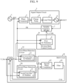
- FIG. 9 is a configuration diagram illustrating the phase-locked loop circuit not covered by by the claimed invention.
- the same reference numerals as those in FIGS. 1 and 7 denote the same or corresponding portions.
- phase-locked loop circuit illustrated in FIG. 9 can output an output signal having the same phase as a phase of an output signal of another phase-locked loop circuit having the same configuration.
- the first subtractor 11, the first integrator 12, the second subtractor 15, and the second integrator 16 are not required, and the circuit scale can be reduced more than that of the phase-locked loop circuit illustrated in FIG. 1 .
- phase-locked loop circuit in which a first phase detection circuit 51 is a first frequency divider 52, and a second phase detection circuit 53 is a second frequency divider 54 will be described.
- FIG. 10 is a configuration diagram illustrating the phase-locked loop circuit not covered by by the claimed invention.
- the same reference numerals as those in FIG. 1 denote the same or corresponding portions, the description thereof will be omitted
- the first phase detection circuit 51 includes the first frequency divider 52.
- the first phase detection circuit 51 calculates the first phase detection signal E1 indicating the phase of the output signal OUT of the VCO 6.
- the first frequency divider 52 divides the output signal OUT of the VCO 6 by M (M is an integer), and outputs the divided signal of the output signal OUT as the first phase detection signal E1 to a second phase comparator 56.
- the second phase detection circuit 53 includes the second frequency divider 54.
- the second phase detection circuit 53 calculates the second phase detection signal E2 indicating the phase of the output signal OUT of a case where it is assumed that the division ratio control circuit 8 controls the division ratio of the output signal OUT of the variable frequency divider 7 in synchronization with the reference signal REF.
- the second frequency divider 54 divides the reference signal REF by L (L is an integer), and outputs the divided signal of the reference signal REF as the second phase detection signal E2 to the second phase comparator 56.
- a shift circuit 55 includes the second phase comparator 56, a filter 57, and the adder 19.
- the shift circuit 55 generates the negative feedback signal CAL and calculates the addition signal of the negative feedback signal CAL and the division ratio setting signal N_frac.
- the second phase comparator 56 detects a phase difference between the divided signal output from the first frequency divider 52 and the divided signal output from the second frequency divider 54, and outputs the phase difference to the filter 57.
- the filter 57 generates the negative feedback signal CAL from the phase difference output from the second phase comparator 56 and outputs the negative feedback signal CAL to the adder 19.
- FIG. 11 is an explanatory diagram illustrating waveforms of the reference signal REF, the output signal OUT, the divided signal (REF ⁇ 9) output from the first frequency divider 52, and the divided signal (REF ⁇ 4) output from the second frequency divider 54.
- the first frequency divider 52 and the second frequency divider 54 each are a frequency divider whose division ratio is fixed.
- a phase of the divided signal output from the first frequency divider 52 always corresponds to the phase of the output signal OUT
- a phase of the divided signal output from the second frequency divider 54 always corresponds to a phase of the reference signal REF.
- the second phase comparator 56 detects the phase difference between the divided signal output from the first frequency divider 52 and the divided signal output from the second frequency divider 54, and outputs the phase difference to the filter 57.
- the filter 57 Upon receiving the phase difference from the second phase comparator 56, the filter 57 generates the negative feedback signal CAL that makes the phase difference zero, and outputs the negative feedback signal CAL to the adder 19.
- the adder 19 adds the division ratio setting signal N frac and the negative feedback signal CAL output from the filter 57 together.
- the adder 19 outputs the addition signal of the division ratio setting signal N frac and the negative feedback signal CAL to the first ⁇ modulator 9.
- the operation principle of the phase-locked loop circuit illustrated in FIG. 10 is similar to the operation principle of the phase-locked loop circuit illustrated in FIG. 1 , and negative feedback is applied so that the first phase detection signal E1 becomes equal to the second phase detection signal E2.
- phase-locked loop circuit illustrated in FIG. 10 can output an output signal having the same phase as a phase of an output signal of another phase-locked loop circuit having the same configuration.
- the first subtractor 11, the first integrator 12, the second subtractor 15, and the second integrator 16 are not required, and the circuit scale can be reduced more than that of the phase-locked loop circuit illustrated in FIG. 1 .
- a phase-locked loop circuit in which a first phase detection circuit 58 includes the first frequency divider 52 and a first counter 59, and a second phase detection circuit 60 includes the second frequency divider 54 and a second counter 61 will he described
- FIG. 12 is a configuration diagram illustrating the phase-locked loop circuit according to the seventh example not covered by by the claimed invention.
- FIG. 12 since the same reference numerals as those in FIGS. 1 and 10 denote the same or corresponding portions, the description thereof will be omitted.
- the first phase detection circuit 58 includes the first frequency divider 52 and the first counter 59.
- the first phase detection circuit 58 calculates the first phase detection signal E1 indicating the phase of the output signal OUT of the VCO 6.
- the first counter 59 counts the number of pulses of the divided signal output from the first frequency divider 52, and outputs the number of pulses of the divided signal as the first phase detection signal E1 to the negative feedback signal generating circuit 63.
- the second phase detection circuit 60 includes the second frequency divider 54 and the second counter 61.
- the second phase detection circuit 60 calculates the second phase detection signal E2 indicating the phase of the output signal OUT.
- the second counter 61 counts the number of pulses of the divided signal output from the second frequency divider 54, and outputs the number of pulses of the divided signal as the second phase detection signal E2 to the negative feedback signal generating circuit 63.
- a shift circuit 62 includes the negative feedback signal generating circuit 63 and the adder 19.
- the shift circuit 62 generates the negative feedback signal CAL and calculates the addition signal of the negative feedback signal CAL and the division ratio setting signal N_frac.
- the negative feedback signal generating circuit 63 generates the negative feedback signal CAL from a difference between the number of pulses output from the first counter 59 and the number of pulses output from the second counter 61, and outputs the negative feedback signal CAL to the adder 19.
- the first frequency divider 52 Upon receiving the output signal OUT of the VCO 6, the first frequency divider 52 divides the output signal OUT by M, and outputs the divided signal of the output signal OUT to the first counter 59.
- the first counter 59 counts the number of pulses of the divided signal output from the first frequency divider 52, and outputs the number of pulses of the divided signal as the first phase detection signal E1 to the negative feedback signal generating circuit 63.
- the second frequency divider 54 Upon receiving the reference signal REF, the second frequency divider 54 divides the reference signal REF by L, and outputs the divided signal of the reference signal REF to the second counter 61.
- the second counter 61 counts the number of pulses of the divided signal output from the second frequency divider 54, and outputs the number of pulses of the divided signal as the second phase detection signal E2 to the negative feedback signal generating circuit 63.
- the negative feedback signal generating circuit 63 calculates the difference between the number of pulses output from the first counter 59 and the number of pulses output from the second counter 61.
- the difference in the number of pulses corresponds to the difference between the first phase detection signal E1 and the second phase detection signal E2.
- the negative feedback signal generating circuit 63 generates the negative feedback signal CAL from the difference in the number of pulses and outputs the negative feedback signal CAL to the adder 19.
- the adder 19 adds the division ratio setting signal N frac and the negative feedback signal CAL output from the negative feedback signal generating circuit 63 together.
- the adder 19 outputs the addition signal of the division ratio setting signal N frac and the negative feedback signal CAL to the first ⁇ modulator 9.
- the operation principle of the phase-locked loop circuit illustrated in FIG. 12 is similar to the operation principle of the phase-locked loop circuits illustrated in FIGS. 1 and 10 , and negative feedback is applied so that the first phase detection signal E1 becomes equal to the second phase detection signal E2.
- phase-locked loop circuit illustrated in FIG. 12 can output an output signal having the same phase as a phase of an output signal of another phase-locked loop circuit having the same configuration.
- the negative feedback signal generating circuit 63 Since the negative feedback signal generating circuit 63 detects the difference by digital signal processing, the negative feedback signal generating circuit 63 has higher noise resistance than that of the negative feedback signal generating circuit 18 illustrated in FIG. 1 that detects the difference by analog signal processing.
- phase-locked loop circuit in which a first phase detection circuit 64 includes a first counter 65, and a second phase detection circuit 66 includes a second counter 67 will be described
- FIG. 13 is a configuration diagram illustrating the phase-locked loop circuit according to the eighth example not covered by by the claimed invention.
- the same reference numerals as those in FIGS. 1 and 12 denote the same or corresponding portions, the description thereof will be omitted.
- the first phase detection circuit 64 includes the first counter 65.
- the first phase detection circuit 64 calculates the first phase detection signal E1 indicating the phase of the output signal OUT of the VCO 6.
- the first counter 65 counts the number of pulses of the output signal OUT of the VCO 6.
- the first counter 65 multiplies the number of pulses of the output signal OUT by the reciprocal of the average division ratio of the output signal OUT of the variable frequency divider 7, and outputs the number of pulses after multiplication of the reciprocal of the division ratio as the first phase detection signal E1 to the negative feedback signal generating circuit 63.
- the second phase detection circuit 66 includes the second counter 67.
- the second phase detection circuit 66 calculates the second phase detection signal E2 indicating the phase of the output signal OUT.
- the second counter 67 counts the number of pulses of the reference signal REF, and outputs the number of pulses of the reference signal REF as the second phase detection signal E2 to the negative feedback signal generating circuit 63.
- first phase detection circuit 64 and the second phase detection circuit 66 Since components other than the first phase detection circuit 64 and the second phase detection circuit 66 are similar to those of the phase-locked loop circuit illustrated in FIG. 12 , here, the operation of the first phase detection circuit 64 and the second phase detection circuit 66 will be mainly described.
- the first counter 65 Upon receiving the output signal OUT of the VCO 6, the first counter 65 counts the number of pulses of the output signal OUT.
- the first counter 65 multiplies the number of pulses of the output signal OUT by the reciprocal of the average division ratio of the output signal OUT of the variable frequency divider 7, and outputs the number of pulses after multiplication of the reciprocal of the division ratio as the first phase detection signal E1 to the negative feedback signal generating circuit 63.
- the second counter 67 Upon receiving the reference signal REF, the second counter 67 counts the number of pulses of the reference signal REF, and outputs the number of pulses of the reference signal REF as the second phase detection signal E2 to the negative feedback signal generating circuit 63.
- the negative feedback signal generating circuit 63 calculates a difference between the number of pulses output from the first counter 65 and the number of pulses output from the second counter 67.
- the negative feedback signal generating circuit 63 generates the negative feedback signal CAL from the difference in the number of pulses and outputs the negative feedback signal CAL to the adder 19.
- the adder 19 adds the division ratio setting signal N_frac and the negative feedback signal CAL output from the negative feedback signal generating circuit 63 together.
- the adder 19 outputs the addition signal of the division ratio setting signal N frac and the negative feedback signal CAL to the first ⁇ modulator 9.
- the operation principle of the phase-locked loop circuit illustrated in FIG. 13 is similar to the operation principle of the phase-locked loop circuits illustrated in FIGS. 1 and 12 , and negative feedback is applied so that the first phase detection signal E1 becomes equal to the second phase detection signal E2.
- phase-locked loop circuit illustrated in FIG. 13 can output an output signal having the same phase as a phase of an output signal of another phase-locked loop circuit having the same configuration.
- the first phase detection circuit 64 does not include the first frequency divider 52, and is smaller in circuit scale than the first phase detection circuit 58 illustrated in FIG. 12 by that amount of the first frequency divider 52.
- the second phase detection circuit 66 does not include the second frequency divider 54, and is smaller in circuit scale than the second phase detection circuit 60 illustrated in FIG. 12 by the amount of the second frequency divider 54.
- a phase-locked loop circuit in which a first phase detection circuit 68 includes a first counter 69, and the second phase detection circuit 66 includes the second counter 67 will be described
- FIG. 14 is a configuration diagram illustrating the phase-locked loop circuit according to the ninth example, not covered by by the claimed invention.
- the same reference numerals as those in FIGS. 1 and 13 denote the same or corresponding portions, the description thereof will be omitted
- the first phase detection circuit 68 includes the first counter 69.
- the first phase detection circuit 68 calculates the first phase detection signal E1 indicating the phase of the output signal OUT of the VCO 6.
- the first counter 69 counts the number of pulses of the divided signal FB output from the variable frequency divider 7, and outputs the number of pulses of the divided signal FB as the first phase detection signal E1 to the negative feedback signal generating circuit 63.
- first phase detection circuit 68 and the second phase detection circuit 66 Since components other than the first phase detection circuit 68 and the second phase detection circuit 66 are similar to those of the phase-locked loop circuit illustrated in FIG. 13 , here, the operation of the first phase detection circuit 68 and the second phase detection circuit 66 will be mainly described.
- the first counter 69 Upon receiving the divided signal FB from the variable frequency divider 7, the first counter 69 counts the number of pulses of the divided signal FB, and outputs the number of pulses of the divided signal FB as the first phase detection signal E1 to the negative feedback signal generating circuit 63.
- the second counter 67 Upon receiving the reference signal REF, the second counter 67 counts the number of pulses of the reference signal REF, and outputs the number of pulses of the reference signal REF as the second phase detection signal E2 to the negative feedback signal generating circuit 63.
- the negative feedback signal generating circuit 63 calculates a difference between the number of pulses output from the first counter 69 and the number of pulses output from the second counter 67.
- the negative feedback signal generating circuit 63 generates the negative feedback signal CAL from the difference in the number of pulses and outputs the negative feedback signal CAL to the adder 19.
- the adder 19 adds the division ratio setting signal N_frac and the negative feedback signal CAL output from the negative feedback signal generating circuit 63 together.
- the adder 19 outputs the addition signal of the division ratio setting signal N_frac and the negative feedback signal CAL to the first ⁇ modulator 9.
- the operation principle of the phase-locked loop circuit illustrated in FIG. 14 is the same as the operation principle of the phase-locked loop circuits illustrated in FIGS. 1 and 13 , and negative feedback is applied so that the first phase detection signal E1 becomes equal to the second phase detection signal E2.
- phase-locked loop circuit illustrated in FIG. 14 can output an output signal having the same phase as a phase of an output signal of another phase-locked loop circuit having the same configuration.
- the first phase detection circuit 68 does not include the first frequency divider 52, and is smaller in circuit scale than the first phase detection circuit 58 illustrated in FIG. 12 by the amount of the first frequency divider 52.
- the second phase detection circuit 66 does not include the second frequency divider 54, and is smaller in circuit scale than the second phase detection circuit 60 illustrated in FIG. 12 by the amount of the second frequency divider 54.
- the first counter 69 counts the number of pulses of the divided signal FB output from the variable frequency divider 7, a required operation speed is reduced more than that required for the first counter 65 illustrated in FIG. 13 for counting the output signal OUT.
- phase-locked loop circuit that includes a delay control circuit 71 for controlling a delay of the first pulse train on the basis of the difference between the first phase detection signal E1 and the second phase detection signal E2 will be described.
- FIG. 15 is a configuration diagram illustrating the phase-locked loop circuit according to the tenth example, not covered by by the claimed invention.
- FIG. 15 since the same reference numerals as those in FIG. 1 denote the same or corresponding portions, the description thereof will be omitted.
- the delay control circuit 71 includes a difference calculation circuit 72 and a delay device 73.
- the delay control circuit 71 calculates the difference between the first phase detection signal E1 output from the first integrator 12 and the second phase detection signal E2 output from the second integrator 16.
- the delay control circuit 71 delays the first pulse train output from the first ⁇ modulator 9 on the basis of the difference between the first phase detection signal E1 and the second phase detection signal E2, and controls the division ratio of the output signal OUT of the variable frequency divider 7 by using the delayed first pulse train.
- the difference calculation circuit 72 calculates the difference between the first phase detection signal E1 output from the first integrator 12 and the second phase detection signal E2 output from the second integrator 16, and outputs a delay time DEL corresponding to the difference to the delay device 73.
- the delay device 73 delays the first pulse train output from the first ⁇ modulator 9 by the delay time DEL output from the difference calculation circuit 72, and outputs the delayed first pulse train as the division ratio control signal N CTRL to the variable frequency divider 7.
- the first ⁇ modulator 9 generates the first pulse train used for controlling the division ratio of the output signal OUT of the variable frequency divider 7 by performing the ⁇ modulation of the division ratio setting signal N frac, in synchronization with the divided signal FB output from the variable frequency divider 7.
- the first ⁇ modulator 9 outputs the first pulse train to the delay device 73.
- the delay device 73 Upon receiving the first pulse train from the first ⁇ modulator 9, the delay device 73 delays the first pulse train by the delay time DEL output from the difference calculation circuit 72, and outputs the delayed first pulse train to the first subtractor 11.
- the delay device 73 outputs the delayed first pulse train as the division ratio control signal N_CTRL to the variable frequency divider 7.
- the first subtractor 11 Upon receiving the first pulse train from the delay device 73, the first subtractor 11 subtracts the division ratio setting signal N_frac from the first pulse train, and outputs a subtraction signal indicating a result of the subtraction to the first integrator 12.
- the first integrator 12 calculates the first phase detection signal E1 by integrating the subtraction signal output from the first subtractor 11, and outputs the first phase detection signal E1 to the difference calculation circuit 72.
- the difference calculation circuit 72 calculates the difference between the first phase detection signal E1 output from the first integrator 12 and the second phase detection signal E2 output from the second integrator 16.
- the difference calculation circuit 72 outputs the delay time DEL corresponding to the difference to the delay device 73 so that the difference between the first phase detection signal E1 and the second phase detection signal E2 becomes zero.
- the difference calculation circuit 72 outputs, to the delay device 73, a delay time longer than the delay time DEL output to the delay device 73 last time.
- the difference calculation circuit 72 outputs, to the delay device 73, a delay time shorter than the delay time DEL output to the delay device 73 last time.
- the difference calculation circuit 72 outputs, to the delay device 73, the same delay time as the delay time DEL output to the delay device 73 last time.
- the delay device 73 delays the first pulse train output from the first ⁇ modulator 9 by the delay time DEL output from the difference calculation circuit 72, and outputs the delayed first pulse train as the division ratio control signal N_CTRL to the variable frequency divider 7.
- the delay device 73 outputs the delayed first pulse train to the first subtractor 11.
- the phase-locked loop circuit illustrated in FIG. 15 delays the first pulse train output from the first ⁇ modulator 9, and is different in this point from the phase-locked loop circuit illustrated in FIG. 1 in which the negative feedback signal CAL is added to the division ratio setting signal N_frac that is the input signal of the first ⁇ modulator 9.
- phase-locked loop circuit illustrated in FIG. 15 is similar to the phase-locked loop circuit illustrated in FIG. 1 in that negative feedback is applied so that the first phase detection signal E1 becomes equal to the second phase detection signal E2.
- the phase-locked loop circuit includes: a division ratio control circuit 8 generating a first pulse train to be used for controlling a division ratio of the output signal of the variable frequency divider 7 from a division ratio setting signal indicating the division ratio, in synchronization with the divided signal output from the variable frequency divider 7; a first phase detection circuit 10 calculating a first phase detection signal indicating a phase of the output signal of the signal output circuit 3; a second phase detection circuit 13 calculating a second phase detection signal indicating a phase of the output signal of a case where it is assumed that the division ratio control circuit 8 generates the first pulse train in synchronization with the reference signal; and a delay control circuit 71 delaying the first pulse train on a basis of a difference between the first phase detection signal and the second phase detection signal, and controlling the division ratio of the output signal of the variable frequency divider 7 by a delayed first pulse train.
- the phase-locked loop circuit of the tenth example can output an output signal having the same phase as a phase of an output
- the present invention is suitable for a phase-locked loop circuit for outputting a signal having a frequency corresponding to a phase difference between a reference signal and a divided signal.
Landscapes
- Stabilization Of Oscillater, Synchronisation, Frequency Synthesizers (AREA)
Description
- The present invention relates to a phase-locked loop circuit for outputting a signal having a frequency corresponding to a phase difference between a reference signal and a divided signal.
- A phase-locked loop circuit includes a phase comparator for detecting a phase difference between a reference signal and a divided signal output from a variable frequency divider, and a charge pump for outputting a current directly proportional to the phase difference detected by the phase comparator.
- Furthermore, the phase-locked loop circuit includes a loop filter for converting the output current of the charge pump into a voltage signal and applying the voltage signal to a frequency control terminal of a voltage controlled oscillator (hereinafter referred to as a "VCO"), and the VCO for outputting a signal having a frequency corresponding to the voltage signal.
- Moreover, the phase-locked loop circuit includes the variable frequency divider for dividing an output signal of the VCO and outputting a divided signal of the output signal to the phase comparator.
- In the phase-locked loop circuit, a ΔΣ modulator can equivalently implement fractional division by randomly modulating a division ratio of the variable frequency divider.
- A pattern of a division ratio control signal output from the ΔΣ modulator to the variable frequency divider corresponds to a phase of the output signal of the VCO, and if the pattern of the division ratio control signal can be controlled, the phase of the output signal of the VCO can be controlled.
- Non-Patent
Literature 1 below discloses a method of controlling the pattern of the division ratio control signal by adding a signal corresponding to an amount of phase control to be implemented to an input signal of the ΔΣ modulator. -
US 2014/0159787 A1 discloses a spread-spectrum clock generator including a frequency comparator, for generating a compensation signal according to a reference signal and a frequency signal corresponding to an output frequency signal. -
US 2017/0338940 A1 discloses a phase discontinuity mitigation implementation within a phase locked loop.
US 2013/ 234800 A1 discloses a calibration device for calibrating an oscillating frequency of an oscillator -
-
Patent Literature 1:
US patent application publication number 0159787 A1 -
Patent Literature 2:
US patent application publication number 0338940 A1 -
Patent Literature 3:
US patent application publication number 0234800 A1 - Non-Patent Literature 1: Hideyuki Nakamizo, Kenichi Tajima "Phase difference control circuit of fractional-N PLL without reset timing control" IEICE General Conference, C-2-102, March 2017
- If the method disclosed in
Non-Patent Literature 1 is used, the pattern of the division ratio control signal can be controlled in the phase-locked loop circuit. - However, even if the input signal of the ΔΣ modulator is the same, the pattern of the division ratio control signal output from the ΔΣ modulator is not always the same, and any one of a plurality of patterns corresponding to one input signal is output from the ΔΣ modulator.
- If the pattern of the division ratio control signal output from the ΔΣ modulator is different, the phase of the output signal of the VCO is different.
- Thus, in a communication apparatus or the like in which a plurality of phase-locked loop circuits having the same configuration is mounted, even if the same input signal is given to ΔΣ modulators of the respective phase-locked loop circuits, there is a case where the phases of the output signals of the plurality of phase-locked loop circuits are different from each other. There has been a problem that, as a result of the phase difference in the output signals of the plurality of phase-locked loop circuits, malfunction occurs in some cases
- The present invention has been made to solve the problem as described above, and an object of the present invention is to obtain a phase-locked loop circuit capable of outputting an output signal having the same phase as a phase of an output signal of another phase-locked loop circuit having the same configuration.
- A phase-locked loop circuit according to the present invention is provided as set forth in
claim 1. - According to the present invention, the phase-locked loop circuit is provided as set forth in
claim 1. Thus, the phase-locked loop circuit according to the present invention can output an output signal having the same phase as a phase of an output signal of another phase-locked loop circuit having the same configuration. -
-
FIG. 1 is a configuration diagram illustrating a phase-locked loop circuit according to a first embodiment. -
FIG. 2 is an explanatory diagram illustrating that a quantization error of ΔΣ modulation of afirst ΔΣ modulator 9 and an instantaneous value of a phase difference Δθ detected by aphase comparator 2 correspond to each other, and a phase of an output signal OUT and a phase indicated by a first phase detection signal E1 correspond to each other. -
FIG. 3 is an explanatory diagram illustrating an example of generation of a negative feedback signal CAL by a negative feedbacksignal generating circuit 18. -
FIG. 4 is a configuration diagram illustrating a phase-locked loop circuit not covered by by the claimed invention. -
FIG. 5 is a configuration diagram illustrating a first first-order ΔΣ modulator 23 of the phase-locked loop circuit not covered by by the claimed invention. -
FIG. 6 is an explanatory diagram illustrating an example of an error output E (= E1) and a carry output C (= C1) of ΔΣ modulation of the first first-order ΔΣ modulator 23, and an error output E (= E2) and a carry output C (= C2) of ΔΣ modulation of a second first-order ΔΣ modulator 27. -
FIG. 7 is a configuration diagram illustrating a phase-locked loop circuit not covered by by the claimed invention. -
FIG. 8 is a configuration diagram illustrating a phase-locked loop circuit not covered by by the claimed invention. -
FIG. 9 is a configuration diagram illustrating a phase-locked loop circuit not covered by by the claimed invention. -
FIG. 10 is a configuration diagram illustrating a phase-locked loop circuit not covered by by the claimed invention. -
FIG. 11 is an explanatory diagram illustrating waveforms of a reference signal REF, the output signal OUT, a divided signal (REF ÷ 9) output from afirst frequency divider 52, and a divided signal (REF ÷ 4) output from asecond frequency divider 54. -
FIG. 12 is a configuration diagram illustrating a phase-locked loop circuit not covered by by the claimed invention. -
FIG. 13 is a configuration diagram illustrating a phase-locked loop circuit not covered by by the claimed invention. -
FIG. 14 is a configuration diagram illustrating a phase-locked loop circuit not covered by by the claimed invention. -
FIG. 15 is a configuration diagram illustrating a phase-locked loop circuit not covered by by the claimed invention. - Hereinafter, to explain the present invention in more detail, embodiments for carrying out the present invention will be described with reference to the accompanying drawings.
-
FIG. 1 is a configuration diagram illustrating a phase-locked loop circuit according to a first embodiment. - In
FIG. 1 , asignal source 1 outputs a reference signal REF to each of aphase comparator 2 and asecond ΔΣ modulator 14. - The
phase comparator 2 detects a phase difference Δθ between the reference signal REF output from thesignal source 1 and a divided signal FB output from avariable frequency divider 7, and outputs an error signal indicating the phase difference Δθ to acharge pump 4. - A
signal output circuit 3 includes thecharge pump 4, aloop filter 5, and a voltage controlled oscillator (VCO) 6. - The
signal output circuit 3 outputs a signal having a frequency corresponding to the error signal output from the phase comparator 2 (hereinafter, referred to as an "output signal OUT") to each of the outside and thevariable frequency divider 7. - The charge pump 4 outputs, to the
loop filter 5, a current directly proportional to the error signal output from thephase comparator 2. - The
loop filter 5 is implemented by a low pass filter or the like. - The
loop filter 5 converts the output current of thecharge pump 4 into a DC voltage and applies the DC voltage to a frequency control terminal of theVCO 6. - The
VCO 6 outputs the output signal OUT having a frequency corresponding to the DC voltage applied to the frequency control terminal to each of the outside and thevariable frequency divider 7. - In the
variable frequency divider 7, a division ratio is set in accordance with a division ratio control signal N CTRL output from afirst ΔΣ modulator 9. - The
variable frequency divider 7 divides the output signal OUT of theVCO 6 by the division ratio set by the division ratio control signal N CTRL, and outputs the divided signal FB of the output signal OUT to each of thephase comparator 2 and thefirst ΔΣ modulators 9. - A division
ratio control circuit 8 includes thefirst ΔΣ modulator 9. - The division
ratio control circuit 8 controls the division ratio of the output signal OUT of thevariable frequency divider 7 on the basis of an addition signal output from anadder 19, in synchronization with the divided signal FB output from thevariable frequency divider 7. - The
first ΔΣ modulator 9 generates a first pulse train for controlling the division ratio of the output signal OUT of thevariable frequency divider 7 by performing ΔΣ modulation of the addition signal output from theadder 19, in synchronization with the divided signal FB output from thevariable frequency divider 7. - The
first ΔΣ modulator 9 outputs the first pulse train as the division ratio control signal N CTRL to each of thevariable frequency divider 7 and afirst subtractor 11. - Note that, the first pulse train generated by the
first ΔΣ modulator 9 means a concept including not only a series of pulses having a signal level of "1" or "0" but also a series of multi-bit digital signals. - A first quantization
error detection circuit 10 includes thefirst subtractor 11 and afirst integrator 12. - The first quantization
error detection circuit 10 calculates a first phase detection signal E1 indicating a phase of the output signal OUT of theVCO 6, and outputs the first phase detection signal E1 to a negative feedbacksignal generating circuit 18. - The
first subtractor 11 subtracts the addition signal output from theadder 19 from the first pulse train output from thefirst ΔΣ modulator 9, and outputs a subtraction signal indicating a result of the subtraction to thefirst integrator 12. - The
first integrator 12 calculates the first phase detection signal E1 by integrating the subtraction signal output from thefirst subtractor 11, and outputs the first phase detection signal E1 to the negative feedbacksignal generating circuit 18. - A second quantization
error detection circuit 13 includes thesecond ΔΣ modulator 14, asecond subtractor 15, and asecond integrator 16. - The second quantization
error detection circuit 13 calculates a second phase detection signal E2 indicating a phase of the output signal OUT of a case where it is assumed that thefirst ΔΣ modulator 9 controls the division ratio of the output signal OUT of thevariable frequency divider 7 in synchronization with the reference signal REF. - The second quantization
error detection circuit 13 outputs the second phase detection signal E2 to the negative feedbacksignal generating circuit 18. - The
second ΔΣ modulator 14 generates a second pulse train by performing ΔΣ modulation of a division ratio setting signal N frac indicating the division ratio, in synchronization with the reference signal REF output from thesignal source 1, and outputs the second pulse train to thesecond subtractor 15. - Note that, the second pulse train generated by the
second ΔΣ modulator 14 means a concept including not only a series of pulses having a signal level of "1" or "0" but also a series of multi-bit digital signals. - The
second subtractor 15 subtracts the division ratio setting signal N_frac from the second pulse train output from thesecond ΔΣ modulator 14, and outputs a subtraction signal indicating a result of the subtraction to thesecond integrator 16. - The
second integrator 16 calculates the second phase detection signal E2 by integrating the subtraction signal output from thesecond subtractor 15, and outputs the second quantization error detection signal E2 to the negative feedbacksignal generating circuit 18. - A
shift circuit 17 includes the negative feedbacksignal generating circuit 18 and theadder 19. - The
shift circuit 17 generates a negative feedback signal CAL from a difference between the first quantization error detection signal E1 output from thefirst integrator 12 and the second quantization error detection signal E2 output from thesecond integrator 16. - The
shift circuit 17 outputs an addition signal of the generated negative feedback signal CAL and the division ratio setting signal N frac to each of thefirst ΔΣ modulator 9 and thefirst subtracter 11 - The negative feedback
signal generating circuit 18 generates the negative feedback signal CAL from the difference between the first quantization error detection signal E1 output from thefirst integrator 12 and the second quantization error detection signal E2 output from thesecond integrator 16, and outputs the negative feedback signal CAL to theadder 19. - The
adder 19 adds the division ratio setting signal N frac and the negative feedback signal CAL output from the negative feedbacksignal generating circuit 18 together, and outputs the addition signal of the division ratio setting signal N frac and the negative feedback signal CAL to each of thefirst ΔΣ modulator 9 and thefirst subtractor 11. - Next, the operation of the phase-locked loop circuit illustrated in
FIG. 1 will be described - The
signal source 1 outputs the reference signal REF to each of thephase comparator 2 and thesecond ΔΣ modulator 14. - Upon receiving the reference signal REF from the
signal source 1 and the divided signal FB from thevariable frequency divider 7, thephase comparator 2 detects the phase difference Δθ between the reference signal REF and the divided signal FB, and outputs the error signal indicating the phase difference Δθ to thecharge pump 4. - Upon receiving the error signal from the
phase comparator 2, thecharge pump 4 outputs the current directly proportional to the error signal to theloop filter 5. - The
loop filter 5 converts the output current of thecharge pump 4 into the DC voltage and applies the DC voltage to the frequency control terminal of theVCO 6. - When the DC voltage is applied to the frequency control terminal by the
loop filter 5, theVCO 6 outputs the output signal OUT having the frequency corresponding to the DC voltage to each of the outside and thevariable frequency divider 7. - In the
variable frequency divider 7, the division ratio is set by the division ratio control signal N_CTRL output from thefirst ΔΣ modulator 9. - The
variable frequency divider 7 divides the output signal OUT of theVCO 6 by the division ratio set by the division ratio control signal N CTRL, and outputs the divided signal FB of the output signal OUT to each of thephase comparator 2 and thefirst ΔΣ modulators 9. - The
adder 19 adds the division ratio setting signal N frac and the negative feedback signal CAL output from the negative feedbacksignal generating circuit 18 together. The division ratio setting signal N frac is a signal indicating a fixed division ratio given from the outside. - The
adder 19 outputs the addition signal of the division ratio setting signal N_frac and the negative feedback signal CAL to each of thefirst ΔΣ modulator 9 and thefirst subtractor 11. - The
first ΔΣ modulator 9 generates the first pulse train for controlling the division ratio of the output signal OUT of thevariable frequency divider 7 by performing the ΔΣ modulation of the addition signal output from theadder 19, in synchronization with the divided signal FB output from thevariable frequency divider 7. - The
first ΔΣ modulator 9 outputs the first pulse train as the division ratio control signal N CTRL to each of thevariable frequency divider 7 and thefirst subtracter 11 - The
first subtractor 11 subtracts the addition signal output from theadder 19 from the first pulse train output from thefirst ΔΣ modulator 9, and outputs the subtraction signal indicating the result of the subtraction to thefirst integrator 12. - The
first integrator 12 calculates the first quantization error detection signal E1 by integrating the subtraction signal output from thefirst subtractor 11, and outputs the first quantization error detection signal E1 to the negative feedbacksignal generating circuit 18. - Here, the subtraction signal output from the
first subtractor 11 corresponds to a quantization error of the ΔΣ modulation of thefirst ΔΣ modulator 9. Furthermore, the quantization error of the ΔΣ modulation corresponds to an instantaneous value of the phase difference Δθ indicated by the error signal output from thephase comparator 2, as illustrated inFIG. 2 -
FIG. 2 is an explanatory diagram illustrating that the quantization error of the ΔΣ modulation of thefirst ΔΣ modulator 9 and the instantaneous value of the phase difference Δθ detected by thephase comparator 2 correspond to each other, and the phase of the output signal OUT and a phase indicated by the first quantization error detection signal E1 correspond to each other. - In the
signal output circuit 3, theloop filter 5 generates the phase of the output signal OUT of theVCO 6 by smoothing the instantaneous value of the phase difference Δθ detected by thephase comparator 2. Thus, thefirst integrator 12 can calculate the first quantization error detection signal E1 indicating the phase of the output signal OUT by integrating the subtraction signal corresponding to the quantization error. - The
second ΔΣ modulator 14 generates the second pulse train by performing the ΔΣ modulation of the division ratio setting signal N frac, in synchronization with the reference signal REF output from thesignal source 1, and outputs the second pulse train to thesecond subtractor 15. - The
second subtractor 15 subtracts the division ratio setting signal N_frac from the second pulse train output from thesecond ΔΣ modulator 14, and outputs the subtraction signal indicating the result of the subtraction to thesecond integrator 16. - The
second integrator 16 calculates the second quantization error detection signal E2 by integrating the subtraction signal output from thesecond subtractor 15, and outputs the second quantization error detection signal E2 to the negative feedbacksignal generating circuit 18. - Here, the subtraction signal output from the
second subtractor 15 corresponds to the quantization error of the ΔΣ modulation of thesecond ΔΣ modulator 14. Thesecond ΔΣ modulator 14 performs the ΔΣ modulation of the division ratio setting signal N frac in synchronization with the reference signal REF. - Furthermore, the circuit configuration including the
second ΔΣ modulator 14, thesecond subtractor 15, and thesecond integrator 16 corresponds to the circuit configuration including thefirst ΔΣ modulator 9, thefirst subtractor 11, and thefirst integrator 12. - Thus, the second quantization error detection signal E2 calculated by the
second integrator 16 indicates the phase of the output signal OUT of a case where it is assumed that thefirst ΔΣ modulator 9 controls the division ratio of the output signal OUT of thevariable frequency divider 7 in synchronization with the reference signal REF. - The negative feedback
signal generating circuit 18 generates the negative feedback signal CAL from the difference (E2 - E1) between the first quantization error detection signal E1 output from thefirst integrator 12 and the second phase quantization error detection signal E2 output from thesecond integrator 16. - That is, the negative feedback
signal generating circuit 18 compares the first quantization error detection signal E1 and the second quantization error detection signal E2 with each other, generates the negative feedback signal CAL to achieve the relation E1 = E2, and outputs the negative feedback signal CAL to theadder 19. -
FIG. 3 is an explanatory diagram illustrating an example of generation of the negative feedback signal CAL by the negative feedbacksignal generating circuit 18. - In
FIG. 3 , it is assumed that each of thefirst ΔΣ modulator 9 and thesecond ΔΣ modulator 14 is a first-order ΔΣ modulator, and the first quantization error detection signal E1 is delayed by two clocks from the second quantization error detection signal E2. - In the example of
FIG. 3 , the negative feedbacksignal generating circuit 18 sets the negative feedback signal CAL to -2N_frac only in a cycle section of one clock, and sets the negative feedback signal CAL to 0 in all other cycle sections. - The negative feedback
signal generating circuit 18 sets the negative feedback signal CAL to -2N frac, whereby the addition signal output from theadder 19 to thefirst ΔΣ modulator 9 is CAL + N_frac = -N_frac, and the first quantization error detection signal E1 changes. The first quantization error detection signal E1 changes, whereby the relation E1 = E2 is achieved. - Thus, since E1 = E2 is achieved in the phase-locked loop circuit illustrated in
FIG. 1 , in a case where, for example, a plurality of the phase-locked loop circuits each having the configuration illustrated inFIG. 1 is mounted on a communication apparatus, it is possible to align phases of the output signals OUT of the plurality of phase-locked loop circuits. - In the first embodiment described above, the phase-locked loop circuit includes: a division
ratio control circuit 8 controlling a division ratio of a divided signal to be output by avariable frequency divider 7 on a basis of an addition signal in which a negative feedback signal is added to a division ratio setting signal indicating a division ratio, in synchronization with the divided signal output from thevariable frequency divider 7; a first quantizationerror detection circuit 10 calculating a first quantization error detection signal indicating a phase of an output signal of asignal output circuit 3; a second quantizationerror detection circuit 13 calculating a second phase detection signal indicating a phase of the output signal of the variable frequency divider in a case where it is assumed that the divisionratio control circuit 8 controls the division ratio of the divided signal to be output by thevariable frequency divider 7 in synchronization with the a signal; and ashift circuit 17 generating the negative feedback signal from a difference between the first quantization error detection signal and the second quantization error detection signal, and outputting the addition signal of the negative feedback signal and the division ratio setting signal to the divisionratio control circuit 8. Thus, the phase-locked loop circuit of the first embodiment can output an output signal having the same phase as a phase of an output signal of another phase-locked loop circuit having the same configuration. - In a second example, not covered by the claimed invention, a phase-locked loop circuit will be described in which a first first-
order ΔΣ modulator 23 is included in a divisionratio control circuit 21, and the first first-order ΔΣ modulator 23 is included in a firstphase detection circuit 22. -
FIG. 4 is a configuration diagram illustrating the phase-locked loop circuit not covered by by the claimed invention. InFIG. 4 , since the same reference numerals as those inFIG. 1 denote the same or corresponding portions, the description thereof will be omitted. - The division
ratio control circuit 21 is a MASH type ΔΣ modulator including the first first-order ΔΣ modulator 23, athird ΔΣ modulator 24, and acombiner 25. - Similarly to the division ratio control circuit illustrated in
FIG. 1 , the divisionratio control circuit 21 controls the division ratio of the output signal OUT of thevariable frequency divider 7 in synchronization with the divided signal FB output from thevariable frequency divider 7 on the basis of the addition signal output from theadder 19. - The first
phase detection circuit 22 includes the first first-order ΔΣ modulator 23. - Similarly to the first
phase detection circuit 10 illustrated inFIG. 1 , the firstphase detection circuit 22 calculates the first phase detection signal E1 indicating the phase of the output signal OUT of theVCO 6. - The first first-
order ΔΣ modulator 23 performs the ΔΣ modulation of the addition signal output from theadder 19 in synchronization with the divided signal FB output from thevariable frequency divider 7. - The first first-
order ΔΣ modulator 23 outputs an error output E of the ΔΣ modulation as the first phase detection signal E1 to each of thethird ΔΣ modulator 24 and a negative feedbacksignal generating circuit 29, and outputs a carry output C of the ΔΣ modulation to thecombiner 25. - The
third ΔΣ modulator 24 performs ΔΣ modulation on the error output E of the first first-order ΔΣ modulator 23 in synchronization with the divided signal FB output from thevariable frequency divider 7, and outputs a carry output C of the ΔΣ modulation to thecombiner 25. - The
combiner 25 is implemented by a delay device, an adder-subtractor, and the like. - The
combiner 25 controls the division ratio of the output signal OUT of thevariable frequency divider 7 on the basis of the carry output C of the ΔΣ modulation of the first first-order ΔΣ modulator 23 and the carry output C of the ΔΣ modulation of thethird ΔΣ modulator 24. - That is, the
combiner 25 obtains the division ratio control signal N_CTRL by combining the carry output C of the ΔΣ modulation of the first first-order ΔΣ modulator 23 and the carry output C of the ΔΣ modulation of thethird ΔΣ modulator 24 together, and outputs the division ratio control signal N_CTRL to thevariable frequency divider 7. - A second
phase detection circuit 26 includes a second first-order ΔΣ modulator 27. - The second
phase detection circuit 26 outputs the second phase detection signal E2 indicating the phase of the output signal OUT of a case where it is assumed that the divisionratio control circuit 21 controls the division ratio of the output signal OUT of thevariable frequency divider 7 in synchronization with the reference signal REF. - The second first-
order ΔΣ modulator 27 performs the ΔΣ modulation of the division ratio setting signal N frac in synchronization with the reference signal REF. - The second first-
order ΔΣ modulator 27 outputs an error output E of the ΔΣ modulation as the second phase detection signal E2 to the negative feedbacksignal generating circuit 29. - A
shift circuit 28 includes the negative feedbacksignal generating circuit 29 and theadder 19. - Similarly to the
shift circuit 17 illustrated inFIG. 1 , theshift circuit 28 generates the negative feedback signal CAL and outputs the addition signal of the negative feedback signal CAL and the division ratio setting signal N frac to the first first-order ΔΣ modulator 23. - The negative feedback
signal generating circuit 29 receives the error output E of the ΔΣ modulation of the first first-order ΔΣ modulator 23 as the first phase detection signal E1, and receives the error output E of the ΔΣ modulation of the second first-order ΔΣ modulator 27 as the second phase detection signal E2. - The negative feedback
signal generating circuit 29 generates the negative feedback signal CAL from a difference between the error output E of the ΔΣ modulation of the first first-order ΔΣ modulator 23 and the error output E of the ΔΣ modulation of the second first-order ΔΣ modulator 27, and outputs the negative feedback signal CAL to theadder 19. -
FIG. 5 is a configuration diagram illustrating the first first-order ΔΣ modulator 23 of the phase-locked loop not covered by the claimed invention. - In
FIG. 5 , asubtractor 31 subtracts an addition signal output from anadder 34 from the addition signal output from theadder 19, and outputs a subtraction signal indicating a result of the subtraction to anadder 32. - The
adder 32 outputs an addition signal of the subtraction signal output from thesubtractor 31 and an output signal of a flip-flop 33 to the flip-flop 33. - The flip-
flop 33 latches the addition signal output from theadder 32 in synchronization with the divided signal FB output from thevariable frequency divider 7, and outputs an output signal that is a logical result to each of theadder 32, theadder 34, and asubtractor 35. - The
adder 34 outputs an addition signal of the output signal of the flip-flop 33 and a quantization error Q to each of thesubtractor 31, thesubtractor 35, and the outsi de - The
subtractor 35 subtracts the output signal of the flip-flop 33 from the addition signal output from theadder 34, and outputs a subtraction signal indicating a result of the subtraction as the error output E to the outside. - Note that, if the division ratio setting signal N_frac is input instead of the addition signal and the reference signal REF is input instead of the divided signal FB, the configuration diagram of
FIG. 5 corresponds to a configuration diagram of the second first-order ΔΣ modulator 27. - Next, the operation of the phase-locked loop circuit illustrated in
FIG. 4 will be described. - Since components other than the division
ratio control circuit 21, the secondphase detection circuit 26, and theshift circuit 28 are similar to those of the phase-locked loop circuit illustrated inFIG. 1 , here, the operation of the divisionratio control circuit 21, the secondphase detection circuit 26, and theshift circuit 28 will be described. - The first first-
order ΔΣ modulator 23 performs the ΔΣ modulation of the addition signal output from theadder 19 in synchronization with the divided signal FB output from thevariable frequency divider 7. - As illustrated in
FIG. 4 , the first first-order ΔΣ modulator 23 outputs the error output E of the ΔΣ modulation as the first phase detection signal E1 to each of thethird ΔΣ modulator 24 and the negative feedbacksignal generating circuit 29, and outputs the carry output C (= C1) of the ΔΣ modulation to thecombiner 25. - The
third ΔΣ modulator 24 performs the ΔΣ modulation of the error output E (= E1) of the first first-order ΔΣ modulator 23 in synchronization with the divided signal FB output from thevariable frequency divider 7. - The
third ΔΣ modulator 24 outputs the carry output C (= C3) of the ΔΣ modulation to thecombiner 25. - The second first-
order ΔΣ modulator 27 performs the ΔΣ modulation of the division ratio setting signal N_frac in synchronization with the reference signal REF. - As illustrated in
FIG. 6 , the second first-order ΔΣ modulator 27 outputs the error output E of the ΔΣ modulation as the second phase detection signal E2 to the negative feedbacksignal generating circuit 29. -
FIG. 6 is an explanatory diagram illustrating an example of the error output E (= E1) and the carry output C (= C 1) of the ΔΣ modulation of the first first-order ΔΣ modulator 23, and the error output E (= E2) and the carry output C (= C2) of the ΔΣ modulation of the second first-order ΔΣ modulator 27. - The
combiner 25 controls the division ratio of the output signal of thevariable frequency divider 7 on the basis of the carry output C (= C1) of the ΔΣ modulation of the first first-order ΔΣ modulator 23 and the carry output C (= C3) of the ΔΣ modulation of thethird ΔΣ modulator 24. - That is, the
combiner 25 obtains the division ratio control signal N_CTRL by combining the carry output C (= C1) of the ΔΣ modulation of the first first-order ΔΣ modulator 23 and the carry output C (= C3) of thethird ΔΣ modulator 24. - The
combiner 25 multiplies each of the carry output C (= C1) and the carry output C (= C3) by a transfer function so that the division ratio control signal N CTRL has desired noise shaping characteristics, and then combines the carry output C1 and carry output C3 together. - The
combiner 25 outputs the division ratio control signal N CTRL to thevariable frequency divider 7. - The negative feedback
signal generating circuit 29 receives the error output E of the ΔΣ modulation of the first first-order ΔΣ modulator 23 as the first phase detection signal E1, and receives the error output E of the ΔΣ modulation of the second first-order ΔΣ modulator 27 as the second phase detection signal E2. - The negative feedback
signal generating circuit 29 generates the negative feedback signal CAL from a difference between the error output E of the ΔΣ modulation of the first first-order ΔΣ modulator 23 and the error output E of the ΔΣ modulation of the second first-order ΔΣ modulator 27, and outputs the negative feedback signal CAL to theadder 19. - The
adder 19 adds the division ratio setting signal N frac and the negative feedback signal CAL output from the negative feedbacksignal generating circuit 29 together. - The
adder 19 outputs the addition signal of the division ratio setting signal N frac and the negative feedback signal CAL to the first first-order ΔΣ modulator 23. - The operation principle of the phase-locked loop circuit illustrated in
FIG. 4 is similar to the operation principle of the phase-locked loop circuit illustrated inFIG. 1 , and negative feedback is applied so that the first phase detection signal E1 becomes equal to the second phase detection signal E2. - Thus, the phase-locked loop circuit illustrated in
FIG. 4 can output an output signal having the same phase as a phase of an output signal of another phase-locked loop circuit having the same configuration. - Furthermore, in the phase-locked loop circuit illustrated in
FIG. 4 , thefirst subtractor 11, thefirst integrator 12, thesecond subtractor 15, and thesecond integrator 16 are not required, and the circuit scale can be reduced more than that of the phase-locked loop circuit illustrated inFIG. 1 . - In a third example, not covered by by the claimed invention, a phase-locked loop circuit in which a
shift circuit 41 includes asecond phase comparator 42, afilter 43, and theadder 19 will be described. -
FIG. 7 is a configuration diagram illustrating the phase-locked loop circuit not covered by by the claimed invention. InFIG. 7 , since the same reference numerals as those inFIGS. 1 and4 denote the same or corresponding portions, the description thereof will be omitted - Similarly to the
shift circuit 28 illustrated inFIG. 4 , theshift circuit 41 generates the negative feedback signal CAL and outputs the addition signal of the negative feedback signal CAL and the division ratio setting signal N_frac to the first first-order ΔΣ modulator 23. - The
second phase comparator 42 detects a phase difference between the carry output C of the ΔΣ modulation of the first first-order ΔΣ modulator 23 and the carry output C of the ΔΣ modulation of the second first-order ΔΣ modulator 27, and outputs the phase difference to thefilter 43. - The
filter 43 generates the negative feedback signal CAL from the phase difference output from thesecond phase comparator 42, and outputs the negative feedback signal CAL to theadder 19. - Next, the operation of the phase-locked loop circuit illustrated in
FIG. 7 will be described. - Since components other than the
second phase comparator 42 and thefilter 43 are similar to those of the phase-locked loop circuit illustrated inFIG. 4 , here, the operation of thesecond phase comparator 42 and thefilter 43 will be described. - In the phase-locked loop circuit illustrated in
FIG. 4 , the negative feedbacksignal generating circuit 29 receives the error output E (= E1) of the ΔΣ modulation of the first first-order ΔΣ modulator 23 and the error output E (= E2) of the ΔΣ modulation of the second first-order ΔΣ modulator 27. - In the phase-locked loop circuit illustrated in
FIG. 7 , thesecond phase comparator 42 receives the carry output C (= C1) of the ΔΣ modulation of the first first-order ΔΣ modulator 23 and the carry output C (= C2) of the ΔΣ modulation of the second first-order ΔΣ modulator 27. - Input signals of the
second phase comparator 42 are different from those of the negative feedbacksignal generating circuit 29. - As illustrated in
FIG. 6 , the carry output C (= C1) of the ΔΣ modulation of the first first-order ΔΣ modulator 23 corresponds to a timing at which the error output E (= E1) of the ΔΣ modulation of the first first-order ΔΣ modulator 23 overflows. - As illustrated in
FIG. 6 , the carry output C (= C2) of the ΔΣ modulation of the second first-order ΔΣ modulator 27 corresponds to a timing at which the error output E (= E2) of the ΔΣ modulation of the second first-order ΔΣ modulator 27 overflows. - The
second phase comparator 42 detects the phase difference between the carry output C (= C1) of the ΔΣ modulation of the first first-order ΔΣ modulator 23 and the carry output C (= C2) of the ΔΣ modulation of the second first-order ΔΣ modulator 27. - The phase difference between the carry outputs C corresponds to the difference between the first phase detection signal E1 and the second phase detection signal E2.
- Upon receiving the phase difference from the
second phase comparator 42, thefilter 43 generates the negative feedback signal CAL that makes the phase difference zero, and outputs the negative feedback signal CAL to theadder 19. - The
adder 19 adds the division ratio setting signal N_frac and the negative feedback signal CAL output from thefilter 43 together. - The
adder 19 outputs the addition signal of the division ratio setting signal N frac and the negative feedback signal CAL to the first first-order ΔΣ modulator 23. - The operation principle of the phase-locked loop circuit illustrated in
FIG. 7 is similar to the operation principle of the phase-locked loop circuits illustrated inFIGS. 1 and4 . Negative feedback is applied so that the carry output C (= C1) of the ΔΣ modulation of the first first-order ΔΣ modulator 23 becomes equal to the carry output C (= C2) of the ΔΣ modulation of the second first-order ΔΣ modulator 27. - Thus, the phase-locked loop circuit illustrated in
FIG. 7 can output an output signal having the same phase as a phase of an output signal of another phase-locked loop circuit having the same configuration. - There are methods of the negative feedback, such as a method discontinuously performed as illustrated in
FIG. 6 , and a method continuously performed by being blunted by a time constant. - When the negative feedback is performed within one clock cycle, the
filter 43 generates a pulsed signal as the negative feedback signal CAL, as illustrated inFIG. 6 . - When the negative feedback is continuously performed, the
filter 43 operates as a low pass filter and applies negative feedback slowly depending on a time constant of the low-pass filter. - In a fourth example, not covered by the claimed invention, a phase-locked loop circuit will be described in which the division
ratio control circuit 8 is thefirst ΔΣ modulator 9, the firstphase detection circuit 22 is the first first-order ΔΣ modulator 23, and the secondphase detection circuit 26 is the second first-order ΔΣ modulator 27, and theshift circuit 28 includes the negative feedbacksignal generating circuit 29. -
FIG. 8 is a configuration diagram illustrating the phase-locked loop circuit not covered by by the claimed invention. InFIG. 8 , the same reference numerals as those inFIGS. 1 and4 denote the same or corresponding portions. - The operation principle of the phase-locked loop circuit illustrated in
FIG. 8 is similar to the operation principle of the phase-locked loop circuits illustrated inFIGS. 1 and4 , and negative feedback is applied so that the first phase detection signal E1 becomes equal to the second phase detection signal E2. - Thus, the phase-locked loop circuit illustrated in
FIG. 8 can output an output signal having the same phase as a phase of an output signal of another phase-locked loop circuit having the same configuration. - Furthermore, in the phase-locked loop circuit illustrated in
FIG. 8 , thefirst subtractor 11, thefirst integrator 12, thesecond subtractor 15, and thesecond integrator 16 are not required, and the circuit scale can be reduced more than that of the phase-locked loop circuit illustrated inFIG. 1 . - In a fifth example, not covered by by the claimed invention, a phase-locked loop circuit will be described in which the division
ratio control circuit 8 is thefirst ΔΣ modulator 9, the firstphase detection circuit 22 is the first first-order ΔΣ modulator 23, and the secondphase detection circuit 26 is the second first-order ΔΣ modulator 27, and theshift circuit 28 includes thesecond phase comparator 42 and thefilter 43. -
FIG. 9 is a configuration diagram illustrating the phase-locked loop circuit not covered by by the claimed invention. InFIG. 9 , the same reference numerals as those inFIGS. 1 and7 denote the same or corresponding portions. - The operation principle of the phase-locked loop circuit illustrated in
FIG. 9 is similar to the operation principle of the phase-locked loop circuit illustrated inFIG. 7 . Negative feedback is applied so that the carry output C (= C1) of the ΔΣ modulation of the first first-order ΔΣ modulator 23 becomes equal to the carry output C (= C2) of the ΔΣ modulation of the second first-order ΔΣ modulator 27. - Thus, the phase-locked loop circuit illustrated in
FIG. 9 can output an output signal having the same phase as a phase of an output signal of another phase-locked loop circuit having the same configuration. - Furthermore, in the phase-locked loop circuit illustrated in
FIG. 9 , thefirst subtractor 11, thefirst integrator 12, thesecond subtractor 15, and thesecond integrator 16 are not required, and the circuit scale can be reduced more than that of the phase-locked loop circuit illustrated inFIG. 1 . - In a sixth example, not covered by by the claimed invention, a phase-locked loop circuit in which a first
phase detection circuit 51 is afirst frequency divider 52, and a secondphase detection circuit 53 is asecond frequency divider 54 will be described. -
FIG. 10 is a configuration diagram illustrating the phase-locked loop circuit not covered by by the claimed invention, InFIG. 10 , since the same reference numerals as those inFIG. 1 denote the same or corresponding portions, the description thereof will be omitted - The first
phase detection circuit 51 includes thefirst frequency divider 52. - Similarly to the first
phase detection circuit 10 illustrated inFIG. 1 , the firstphase detection circuit 51 calculates the first phase detection signal E1 indicating the phase of the output signal OUT of theVCO 6. - The
first frequency divider 52 divides the output signal OUT of theVCO 6 by M (M is an integer), and outputs the divided signal of the output signal OUT as the first phase detection signal E1 to asecond phase comparator 56. - The second
phase detection circuit 53 includes thesecond frequency divider 54. - Similarly to the second
phase detection circuit 13 illustrated inFIG. 1 , the secondphase detection circuit 53 calculates the second phase detection signal E2 indicating the phase of the output signal OUT of a case where it is assumed that the divisionratio control circuit 8 controls the division ratio of the output signal OUT of thevariable frequency divider 7 in synchronization with the reference signal REF. - The
second frequency divider 54 divides the reference signal REF by L (L is an integer), and outputs the divided signal of the reference signal REF as the second phase detection signal E2 to thesecond phase comparator 56. - A
shift circuit 55 includes thesecond phase comparator 56, afilter 57, and theadder 19. - Similarly to the
shift circuit 17 illustrated inFIG. 1 , theshift circuit 55 generates the negative feedback signal CAL and calculates the addition signal of the negative feedback signal CAL and the division ratio setting signal N_frac. - The
second phase comparator 56 detects a phase difference between the divided signal output from thefirst frequency divider 52 and the divided signal output from thesecond frequency divider 54, and outputs the phase difference to thefilter 57. - The
filter 57 generates the negative feedback signal CAL from the phase difference output from thesecond phase comparator 56 and outputs the negative feedback signal CAL to theadder 19. - Next, the operation of the phase-locked loop circuit illustrated in
FIG. 10 will be described. - Since components other than the first
phase detection circuit 51, the secondphase detection circuit 53, and theshift circuit 55 are similar to those of the phase-locked loop circuit illustrated inFIG. 1 , here, the operation of the firstphase detection circuit 51, the secondphase detection circuit 53, and theshift circuit 55 will be described. - First, the division ratio M of the output signal OUT of the
first frequency divider 52 and the division ratio L of the reference signal REF of thesecond frequency divider 54 are selected so that M/L matches an average division ratio (= multiplication ratio of the phase-locked loop circuit) of the output signal OUT of thevariable frequency divider 7. - Here, for convenience of description, the description will be made assuming that the division ratio M of the output signal OUT of the
first frequency divider 52 is 9, the division ratio L of the reference signal REF of thesecond frequency divider 54 is 4, and the average division ratio of the output signal OUT of thevariable frequency divider 7 is M/L = 2.25. -
FIG. 11 is an explanatory diagram illustrating waveforms of the reference signal REF, the output signal OUT, the divided signal (REF ÷ 9) output from thefirst frequency divider 52, and the divided signal (REF ÷ 4) output from thesecond frequency divider 54. - The
first frequency divider 52 and thesecond frequency divider 54 each are a frequency divider whose division ratio is fixed. - In the frequency divider whose division ratio is fixed, unlike the
variable frequency divider 7, only one state exists as a phase state. - Thus, a phase of the divided signal output from the
first frequency divider 52 always corresponds to the phase of the output signal OUT, and a phase of the divided signal output from thesecond frequency divider 54 always corresponds to a phase of the reference signal REF. - The
second phase comparator 56 detects the phase difference between the divided signal output from thefirst frequency divider 52 and the divided signal output from thesecond frequency divider 54, and outputs the phase difference to thefilter 57. - Upon receiving the phase difference from the
second phase comparator 56, thefilter 57 generates the negative feedback signal CAL that makes the phase difference zero, and outputs the negative feedback signal CAL to theadder 19. - The
adder 19 adds the division ratio setting signal N frac and the negative feedback signal CAL output from thefilter 57 together. - The
adder 19 outputs the addition signal of the division ratio setting signal N frac and the negative feedback signal CAL to thefirst ΔΣ modulator 9. - The operation principle of the phase-locked loop circuit illustrated in
FIG. 10 is similar to the operation principle of the phase-locked loop circuit illustrated inFIG. 1 , and negative feedback is applied so that the first phase detection signal E1 becomes equal to the second phase detection signal E2. - Thus, the phase-locked loop circuit illustrated in
FIG. 10 can output an output signal having the same phase as a phase of an output signal of another phase-locked loop circuit having the same configuration. - Furthermore, in the phase-locked loop circuit illustrated in
FIG. 10 , thefirst subtractor 11, thefirst integrator 12, thesecond subtractor 15, and thesecond integrator 16 are not required, and the circuit scale can be reduced more than that of the phase-locked loop circuit illustrated inFIG. 1 . - In a seventh example, not covered by by the claimed invention, a phase-locked loop circuit in which a first
phase detection circuit 58 includes thefirst frequency divider 52 and afirst counter 59, and a secondphase detection circuit 60 includes thesecond frequency divider 54 and asecond counter 61 will he described -
FIG. 12 is a configuration diagram illustrating the phase-locked loop circuit according to the seventh example not covered by by the claimed invention. InFIG. 12 , since the same reference numerals as those inFIGS. 1 and10 denote the same or corresponding portions, the description thereof will be omitted. - The first
phase detection circuit 58 includes thefirst frequency divider 52 and thefirst counter 59. - Similarly to the first
phase detection circuit 10 illustrated inFIG. 1 , the firstphase detection circuit 58 calculates the first phase detection signal E1 indicating the phase of the output signal OUT of theVCO 6. - The
first counter 59 counts the number of pulses of the divided signal output from thefirst frequency divider 52, and outputs the number of pulses of the divided signal as the first phase detection signal E1 to the negative feedbacksignal generating circuit 63. - The second
phase detection circuit 60 includes thesecond frequency divider 54 and thesecond counter 61. - Similarly to the second
phase detection circuit 13 illustrated inFIG. 1 , the secondphase detection circuit 60 calculates the second phase detection signal E2 indicating the phase of the output signal OUT. - The
second counter 61 counts the number of pulses of the divided signal output from thesecond frequency divider 54, and outputs the number of pulses of the divided signal as the second phase detection signal E2 to the negative feedbacksignal generating circuit 63. - A
shift circuit 62 includes the negative feedbacksignal generating circuit 63 and theadder 19. - Similarly to the
shift circuit 17 illustrated inFIG. 1 , theshift circuit 62 generates the negative feedback signal CAL and calculates the addition signal of the negative feedback signal CAL and the division ratio setting signal N_frac. - The negative feedback
signal generating circuit 63 generates the negative feedback signal CAL from a difference between the number of pulses output from thefirst counter 59 and the number of pulses output from thesecond counter 61, and outputs the negative feedback signal CAL to theadder 19. - Next, the operation of the phase-locked loop circuit illustrated in
FIG. 12 will be described. - Since components other than the first
phase detection circuit 58, the secondphase detection circuit 60, and theshift circuit 62 are similar to those of the phase-locked loop circuit illustrated inFIG. 1 , here, the operation of the firstphase detection circuit 58, the secondphase detection circuit 60, and theshift circuit 62 will be described. - Upon receiving the output signal OUT of the
VCO 6, thefirst frequency divider 52 divides the output signal OUT by M, and outputs the divided signal of the output signal OUT to thefirst counter 59. - The
first counter 59 counts the number of pulses of the divided signal output from thefirst frequency divider 52, and outputs the number of pulses of the divided signal as the first phase detection signal E1 to the negative feedbacksignal generating circuit 63. - Upon receiving the reference signal REF, the
second frequency divider 54 divides the reference signal REF by L, and outputs the divided signal of the reference signal REF to thesecond counter 61. - The
second counter 61 counts the number of pulses of the divided signal output from thesecond frequency divider 54, and outputs the number of pulses of the divided signal as the second phase detection signal E2 to the negative feedbacksignal generating circuit 63. - The negative feedback
signal generating circuit 63 calculates the difference between the number of pulses output from thefirst counter 59 and the number of pulses output from thesecond counter 61. - The difference in the number of pulses corresponds to the difference between the first phase detection signal E1 and the second phase detection signal E2.
- The negative feedback
signal generating circuit 63 generates the negative feedback signal CAL from the difference in the number of pulses and outputs the negative feedback signal CAL to theadder 19. - The
adder 19 adds the division ratio setting signal N frac and the negative feedback signal CAL output from the negative feedbacksignal generating circuit 63 together. - The
adder 19 outputs the addition signal of the division ratio setting signal N frac and the negative feedback signal CAL to thefirst ΔΣ modulator 9. - The operation principle of the phase-locked loop circuit illustrated in
FIG. 12 is similar to the operation principle of the phase-locked loop circuits illustrated inFIGS. 1 and10 , and negative feedback is applied so that the first phase detection signal E1 becomes equal to the second phase detection signal E2. - Thus, the phase-locked loop circuit illustrated in
FIG. 12 can output an output signal having the same phase as a phase of an output signal of another phase-locked loop circuit having the same configuration. - Since the negative feedback
signal generating circuit 63 detects the difference by digital signal processing, the negative feedbacksignal generating circuit 63 has higher noise resistance than that of the negative feedbacksignal generating circuit 18 illustrated inFIG. 1 that detects the difference by analog signal processing. - In an eighth example, not covered by by the claimed invention, a phase-locked loop circuit in which a first
phase detection circuit 64 includes afirst counter 65, and a secondphase detection circuit 66 includes asecond counter 67 will be described -
FIG. 13 is a configuration diagram illustrating the phase-locked loop circuit according to the eighth example not covered by by the claimed invention. InFIG. 13 , since the same reference numerals as those inFIGS. 1 and12 denote the same or corresponding portions, the description thereof will be omitted. - The first
phase detection circuit 64 includes thefirst counter 65. - Similarly to the first
phase detection circuit 10 illustrated inFIG. 1 , the firstphase detection circuit 64 calculates the first phase detection signal E1 indicating the phase of the output signal OUT of theVCO 6. - The
first counter 65 counts the number of pulses of the output signal OUT of theVCO 6. - The
first counter 65 multiplies the number of pulses of the output signal OUT by the reciprocal of the average division ratio of the output signal OUT of thevariable frequency divider 7, and outputs the number of pulses after multiplication of the reciprocal of the division ratio as the first phase detection signal E1 to the negative feedbacksignal generating circuit 63. - The second
phase detection circuit 66 includes thesecond counter 67. - Similarly to the second
phase detection circuit 13 illustrated inFIG. 1 , the secondphase detection circuit 66 calculates the second phase detection signal E2 indicating the phase of the output signal OUT. - The
second counter 67 counts the number of pulses of the reference signal REF, and outputs the number of pulses of the reference signal REF as the second phase detection signal E2 to the negative feedbacksignal generating circuit 63. - Next, the operation of the phase-locked loop circuit illustrated in
FIG. 13 will be described - Since components other than the first
phase detection circuit 64 and the secondphase detection circuit 66 are similar to those of the phase-locked loop circuit illustrated inFIG. 12 , here, the operation of the firstphase detection circuit 64 and the secondphase detection circuit 66 will be mainly described. - Upon receiving the output signal OUT of the
VCO 6, thefirst counter 65 counts the number of pulses of the output signal OUT. - The
first counter 65 multiplies the number of pulses of the output signal OUT by the reciprocal of the average division ratio of the output signal OUT of thevariable frequency divider 7, and outputs the number of pulses after multiplication of the reciprocal of the division ratio as the first phase detection signal E1 to the negative feedbacksignal generating circuit 63. - Upon receiving the reference signal REF, the
second counter 67 counts the number of pulses of the reference signal REF, and outputs the number of pulses of the reference signal REF as the second phase detection signal E2 to the negative feedbacksignal generating circuit 63. - The negative feedback
signal generating circuit 63 calculates a difference between the number of pulses output from thefirst counter 65 and the number of pulses output from thesecond counter 67. - The negative feedback
signal generating circuit 63 generates the negative feedback signal CAL from the difference in the number of pulses and outputs the negative feedback signal CAL to theadder 19. - The
adder 19 adds the division ratio setting signal N_frac and the negative feedback signal CAL output from the negative feedbacksignal generating circuit 63 together. - The
adder 19 outputs the addition signal of the division ratio setting signal N frac and the negative feedback signal CAL to thefirst ΔΣ modulator 9. - The operation principle of the phase-locked loop circuit illustrated in
FIG. 13 is similar to the operation principle of the phase-locked loop circuits illustrated inFIGS. 1 and12 , and negative feedback is applied so that the first phase detection signal E1 becomes equal to the second phase detection signal E2. - Thus, the phase-locked loop circuit illustrated in
FIG. 13 can output an output signal having the same phase as a phase of an output signal of another phase-locked loop circuit having the same configuration. - The first
phase detection circuit 64 does not include thefirst frequency divider 52, and is smaller in circuit scale than the firstphase detection circuit 58 illustrated inFIG. 12 by that amount of thefirst frequency divider 52. - Furthermore, the second
phase detection circuit 66 does not include thesecond frequency divider 54, and is smaller in circuit scale than the secondphase detection circuit 60 illustrated inFIG. 12 by the amount of thesecond frequency divider 54. - In a ninth example, not covered by by the claimed invention, a phase-locked loop circuit in which a first
phase detection circuit 68 includes afirst counter 69, and the secondphase detection circuit 66 includes thesecond counter 67 will be described -
FIG. 14 is a configuration diagram illustrating the phase-locked loop circuit according to the ninth example, not covered by by the claimed invention. InFIG. 14 , since the same reference numerals as those inFIGS. 1 and13 denote the same or corresponding portions, the description thereof will be omitted - The first
phase detection circuit 68 includes thefirst counter 69. - Similarly to the first
phase detection circuit 10 illustrated inFIG. 1 , the firstphase detection circuit 68 calculates the first phase detection signal E1 indicating the phase of the output signal OUT of theVCO 6. - The
first counter 69 counts the number of pulses of the divided signal FB output from thevariable frequency divider 7, and outputs the number of pulses of the divided signal FB as the first phase detection signal E1 to the negative feedbacksignal generating circuit 63. - Next, the operation of the phase-locked loop circuit illustrated in
FIG. 14 will be described. - Since components other than the first
phase detection circuit 68 and the secondphase detection circuit 66 are similar to those of the phase-locked loop circuit illustrated inFIG. 13 , here, the operation of the firstphase detection circuit 68 and the secondphase detection circuit 66 will be mainly described. - Upon receiving the divided signal FB from the
variable frequency divider 7, thefirst counter 69 counts the number of pulses of the divided signal FB, and outputs the number of pulses of the divided signal FB as the first phase detection signal E1 to the negative feedbacksignal generating circuit 63. - Upon receiving the reference signal REF, the
second counter 67 counts the number of pulses of the reference signal REF, and outputs the number of pulses of the reference signal REF as the second phase detection signal E2 to the negative feedbacksignal generating circuit 63. - The negative feedback
signal generating circuit 63 calculates a difference between the number of pulses output from thefirst counter 69 and the number of pulses output from thesecond counter 67. - The negative feedback
signal generating circuit 63 generates the negative feedback signal CAL from the difference in the number of pulses and outputs the negative feedback signal CAL to theadder 19. - The
adder 19 adds the division ratio setting signal N_frac and the negative feedback signal CAL output from the negative feedbacksignal generating circuit 63 together. - The
adder 19 outputs the addition signal of the division ratio setting signal N_frac and the negative feedback signal CAL to thefirst ΔΣ modulator 9. - The operation principle of the phase-locked loop circuit illustrated in
FIG. 14 is the same as the operation principle of the phase-locked loop circuits illustrated inFIGS. 1 and13 , and negative feedback is applied so that the first phase detection signal E1 becomes equal to the second phase detection signal E2. - Thus, the phase-locked loop circuit illustrated in
FIG. 14 can output an output signal having the same phase as a phase of an output signal of another phase-locked loop circuit having the same configuration. - The first
phase detection circuit 68 does not include thefirst frequency divider 52, and is smaller in circuit scale than the firstphase detection circuit 58 illustrated inFIG. 12 by the amount of thefirst frequency divider 52. - Furthermore, the second
phase detection circuit 66 does not include thesecond frequency divider 54, and is smaller in circuit scale than the secondphase detection circuit 60 illustrated inFIG. 12 by the amount of thesecond frequency divider 54. - Since the
first counter 69 counts the number of pulses of the divided signal FB output from thevariable frequency divider 7, a required operation speed is reduced more than that required for thefirst counter 65 illustrated inFIG. 13 for counting the output signal OUT. - In a tenth example, not covered by by the claimed invention, a phase-locked loop circuit that includes a
delay control circuit 71 for controlling a delay of the first pulse train on the basis of the difference between the first phase detection signal E1 and the second phase detection signal E2 will be described. -
FIG. 15 is a configuration diagram illustrating the phase-locked loop circuit according to the tenth example, not covered by by the claimed invention. InFIG. 15 , since the same reference numerals as those inFIG. 1 denote the same or corresponding portions, the description thereof will be omitted. - The
delay control circuit 71 includes adifference calculation circuit 72 and adelay device 73. - The
delay control circuit 71 calculates the difference between the first phase detection signal E1 output from thefirst integrator 12 and the second phase detection signal E2 output from thesecond integrator 16. - The
delay control circuit 71 delays the first pulse train output from thefirst ΔΣ modulator 9 on the basis of the difference between the first phase detection signal E1 and the second phase detection signal E2, and controls the division ratio of the output signal OUT of thevariable frequency divider 7 by using the delayed first pulse train. - The
difference calculation circuit 72 calculates the difference between the first phase detection signal E1 output from thefirst integrator 12 and the second phase detection signal E2 output from thesecond integrator 16, and outputs a delay time DEL corresponding to the difference to thedelay device 73. - The
delay device 73 delays the first pulse train output from thefirst ΔΣ modulator 9 by the delay time DEL output from thedifference calculation circuit 72, and outputs the delayed first pulse train as the division ratio control signal N CTRL to thevariable frequency divider 7. - Next, the operation of the phase-locked loop circuit illustrated in
FIG. 15 will be described - Since components other than the
first ΔΣ modulator 9 and thedelay control circuit 71 are similar to those of the phase-locked loop circuit illustrated inFIG. 1 , here, the operation of thefirst ΔΣ modulator 9 and thedelay control circuit 71 will be mainly described - The
first ΔΣ modulator 9 generates the first pulse train used for controlling the division ratio of the output signal OUT of thevariable frequency divider 7 by performing the ΔΣ modulation of the division ratio setting signal N frac, in synchronization with the divided signal FB output from thevariable frequency divider 7. - The
first ΔΣ modulator 9 outputs the first pulse train to thedelay device 73. - Upon receiving the first pulse train from the
first ΔΣ modulator 9, thedelay device 73 delays the first pulse train by the delay time DEL output from thedifference calculation circuit 72, and outputs the delayed first pulse train to thefirst subtractor 11. - Furthermore, the
delay device 73 outputs the delayed first pulse train as the division ratio control signal N_CTRL to thevariable frequency divider 7. - Upon receiving the first pulse train from the
delay device 73, thefirst subtractor 11 subtracts the division ratio setting signal N_frac from the first pulse train, and outputs a subtraction signal indicating a result of the subtraction to thefirst integrator 12. - The
first integrator 12 calculates the first phase detection signal E1 by integrating the subtraction signal output from thefirst subtractor 11, and outputs the first phase detection signal E1 to thedifference calculation circuit 72. - The
difference calculation circuit 72 calculates the difference between the first phase detection signal E1 output from thefirst integrator 12 and the second phase detection signal E2 output from thesecond integrator 16. - The
difference calculation circuit 72 outputs the delay time DEL corresponding to the difference to thedelay device 73 so that the difference between the first phase detection signal E1 and the second phase detection signal E2 becomes zero. - That is, if E1 < E2, the
difference calculation circuit 72 outputs, to thedelay device 73, a delay time longer than the delay time DEL output to thedelay device 73 last time. - If E1 > E2, the
difference calculation circuit 72 outputs, to thedelay device 73, a delay time shorter than the delay time DEL output to thedelay device 73 last time. - If E1 = E2, the
difference calculation circuit 72 outputs, to thedelay device 73, the same delay time as the delay time DEL output to thedelay device 73 last time. - The
delay device 73 delays the first pulse train output from thefirst ΔΣ modulator 9 by the delay time DEL output from thedifference calculation circuit 72, and outputs the delayed first pulse train as the division ratio control signal N_CTRL to thevariable frequency divider 7. - Furthermore, the
delay device 73 outputs the delayed first pulse train to thefirst subtractor 11. - The phase-locked loop circuit illustrated in
FIG. 15 delays the first pulse train output from thefirst ΔΣ modulator 9, and is different in this point from the phase-locked loop circuit illustrated inFIG. 1 in which the negative feedback signal CAL is added to the division ratio setting signal N_frac that is the input signal of thefirst ΔΣ modulator 9. - However, the phase-locked loop circuit illustrated in
FIG. 15 is similar to the phase-locked loop circuit illustrated inFIG. 1 in that negative feedback is applied so that the first phase detection signal E1 becomes equal to the second phase detection signal E2. - In the tenth example described above, the phase-locked loop circuit includes: a division
ratio control circuit 8 generating a first pulse train to be used for controlling a division ratio of the output signal of thevariable frequency divider 7 from a division ratio setting signal indicating the division ratio, in synchronization with the divided signal output from thevariable frequency divider 7; a firstphase detection circuit 10 calculating a first phase detection signal indicating a phase of the output signal of thesignal output circuit 3; a secondphase detection circuit 13 calculating a second phase detection signal indicating a phase of the output signal of a case where it is assumed that the divisionratio control circuit 8 generates the first pulse train in synchronization with the reference signal; and adelay control circuit 71 delaying the first pulse train on a basis of a difference between the first phase detection signal and the second phase detection signal, and controlling the division ratio of the output signal of thevariable frequency divider 7 by a delayed first pulse train. Thus, the phase-locked loop circuit of the tenth example can output an output signal having the same phase as a phase of an output signal of another phase-locked loop circuit having the same configuration. - The present invention is suitable for a phase-locked loop circuit for outputting a signal having a frequency corresponding to a phase difference between a reference signal and a divided signal.
- 1: signal source, 2: phase comparator, 3: signal output circuit, 4: charge pump, 5: loop filter, 6: VCO, 7: variable frequency divider, 8: division ratio control circuit, 9: first ΔΣ modulator, 10: first phase detection circuit, 11: first subtractor, 12: first integrator, 13: second phase detection circuit, 14: second ΔΣ modulator, 15: second subtractor, 16: second integrator, 17: shift circuit, 18: negative feedback signal generating circuit, 19: adder, 21: division ratio control circuit, 22: first phase detection circuit, 23: first first-order ΔΣ modulator, 24: third ΔΣ modulator, 25: combiner, 26: second phase detection circuit, 27: second first-order ΔΣ modulator, 28: shift circuit, 29: negative feedback signal generating circuit, 31, 35: subtractor, 32, 34: adder, 33: flip-flop, 41: shift circuit, 42: second phase comparator, 43: filter, 51: first phase detection circuit, 52: first frequency divider, 53: second phase detection circuit, 54: second frequency divider, 55: shift circuit, 56: second phase comparator, 57: filter, 58: first phase detection circuit, 59: first counter, 60: second phase detection circuit, 61: second counter, 62: shift circuit, 63: negative feedback signal generating circuit, 64: first phase detection circuit, 65: first counter, 66: second phase detection circuit, 67: second counter, 68: first phase detection circuit, 69: first counter, 71: delay control circuit, 72: difference calculation circuit, 73: delay device
Claims (1)
- A phase-locked loop circuit comprising:a phase comparator (2) configured to detect a phase difference between a reference signal (REF) and a divided signal (FB);a signal output circuit (3) configured to output an output signal (OUT) having a frequency corresponding to the phase difference detected by the phase comparator (2);a variable frequency divider (7) configured to generate the divided signal (FB) by dividing the output signal (OUT) of the signal output circuit and outputting the divided signal (FB) of the output signal (OUT) to the phase comparator (2);a division ratio control circuit (8) configured to control a division ratio (N_CTRL) of the divided signal (FB) to be output by the variable frequency divider (7) on a basis of an addition signal in which a negative feedback signal (CAL) is added to a division ratio setting signal (N_frac) indicating a division ratio, in synchronization with the divided signal (FB) from the variable frequency divider (7) wherein the division ratio control circuit is a first ΔΣ modulator (9) configured to generate a first pulse train indicating the division ratio of the output signal (OUT) of the variable frequency divider (7) by performing ΔΣ modulation of the addition signal, in synchronization with the divided signal output (FB) from the variable frequency divider (7);a first quantization error detection circuit (10, 22, 51, 58, 64, 68) including:a first subtractor (11) configured to perform subtraction subtracting the addition signal from the first pulse train generated by the first ΔΣ modulator; anda first integrator (12) configured to calculate a first quantization error detection signal (E 1) by integrating a result of the subtraction performed by the first subtractor (11);wherein the first quantization error detection circuit (10, 22, 51, 58, 64, 68) is configured to calculate the first quantization error detection signal (E1) indicating a quantization error of the first ΔΣ modulator (9);a second quantization error detection circuit (13, 26, 53, 60, 66) including:a second ΔΣ modulator (14) configured to generate a second pulse train by performing ΔΣ modulation of the division ratio setting signal (N_frac), in synchronization with the reference signal (REF);a second subtractor (15) configured to perform subtraction subtracting the division ratio setting signal (N_frac) from the second pulse train generated by the second ΔΣ modulator (14); anda second integrator (16) configured to calculate the second quantization error detection signal (E2) by integrating a result of the subtraction performed by the second subtractor (15);wherein the second quantization error detection circuit (13, 26, 53, 60, 66) is configured to calculate a second quantization error detection signal (E2) indicating a quantization error of the second ΔΣ modulator (14) in a case where it is assumed that the division ratio control circuit (8) controls the division ratio of the divided signal (FB) to be output by the variable frequency divider (7) in synchronization with the reference signal (REF);a negative feedback signal generating circuit (18) to generate the negative feedback signal (CAL) from a difference between the first quantization error detection signal (E1) and the second quantization error detection signal (E2); andan adder (19) to output the addition signal to the division ratio control circuit (8).
Applications Claiming Priority (1)
| Application Number | Priority Date | Filing Date | Title |
|---|---|---|---|
| PCT/JP2018/026039 WO2020012557A1 (en) | 2018-07-10 | 2018-07-10 | Phase-locked loop circuit |
Publications (3)
| Publication Number | Publication Date |
|---|---|
| EP3806338A1 EP3806338A1 (en) | 2021-04-14 |
| EP3806338A4 EP3806338A4 (en) | 2021-06-23 |
| EP3806338B1 true EP3806338B1 (en) | 2023-05-10 |
Family
ID=69141666
Family Applications (1)
| Application Number | Title | Priority Date | Filing Date |
|---|---|---|---|
| EP18925993.0A Active EP3806338B1 (en) | 2018-07-10 | 2018-07-10 | Phase-locked loop circuit |
Country Status (4)
| Country | Link |
|---|---|
| US (1) | US11088698B2 (en) |
| EP (1) | EP3806338B1 (en) |
| JP (1) | JP6779419B2 (en) |
| WO (1) | WO2020012557A1 (en) |
Families Citing this family (3)
| Publication number | Priority date | Publication date | Assignee | Title |
|---|---|---|---|---|
| JP7534667B2 (en) | 2020-02-20 | 2024-08-15 | 株式会社ソシオネクスト | Phase locked loop circuit, transmitter/receiver circuit, and semiconductor integrated circuit |
| JP7301766B2 (en) * | 2020-03-04 | 2023-07-03 | 株式会社東芝 | PHASE CORRECTOR, RANGING DEVICE AND PHASE VARIATION DETECTION DEVICE |
| TWI746411B (en) * | 2021-05-24 | 2021-11-11 | 穩脈科技股份有限公司 | Clock generating circuit and calibration circuit thereof |
Family Cites Families (7)
| Publication number | Priority date | Publication date | Assignee | Title |
|---|---|---|---|---|
| JP4757181B2 (en) * | 2006-12-05 | 2011-08-24 | アンリツ株式会社 | Signal generator |
| JP2012147080A (en) * | 2011-01-07 | 2012-08-02 | Panasonic Corp | Delta-sigma modulation-type fraction division pll frequency synthesizer, and wireless communication device having the same |
| US8896386B2 (en) * | 2012-03-08 | 2014-11-25 | Mediatek Singapore Pte. Ltd. | Calibration device for oscillator and method thereof |
| JP5787849B2 (en) * | 2012-08-29 | 2015-09-30 | 三菱電機株式会社 | Frequency synthesizer |
| TW201424271A (en) * | 2012-12-12 | 2014-06-16 | Novatek Microelectronics Corp | Spread-spectrum clock generator |
| US9893875B2 (en) * | 2016-05-23 | 2018-02-13 | Qualcomm Incorporated | Phase continuity technique for frequency synthesis |
| JP6494888B2 (en) * | 2016-12-19 | 2019-04-03 | 三菱電機株式会社 | PLL circuit |
-
2018
- 2018-07-10 WO PCT/JP2018/026039 patent/WO2020012557A1/en unknown
- 2018-07-10 EP EP18925993.0A patent/EP3806338B1/en active Active
- 2018-07-10 JP JP2020529879A patent/JP6779419B2/en not_active Expired - Fee Related
-
2020
- 2020-11-30 US US17/107,382 patent/US11088698B2/en active Active
Also Published As
| Publication number | Publication date |
|---|---|
| JP6779419B2 (en) | 2020-11-04 |
| WO2020012557A1 (en) | 2020-01-16 |
| EP3806338A4 (en) | 2021-06-23 |
| US20210083681A1 (en) | 2021-03-18 |
| US11088698B2 (en) | 2021-08-10 |
| JPWO2020012557A1 (en) | 2020-12-17 |
| EP3806338A1 (en) | 2021-04-14 |
Similar Documents
| Publication | Publication Date | Title |
|---|---|---|
| US11088698B2 (en) | Phase-locked loop circuit | |
| KR100237539B1 (en) | Frequency synthesizer | |
| CN103348596B (en) | Reference clock for fractional-N phase lock loop (PLL) compensates | |
| JP2004519917A (en) | Σ-ΔN frequency divider with improved noise and spur performance | |
| US8826062B2 (en) | Apparatus for synchronizing a data handover between a first clock domain and a second clock domain through phase synchronization | |
| CN108667458A (en) | fractional-N digital P LL capable of eliminating quantization noise from sigma-delta modulators | |
| KR102578322B1 (en) | Asynchronous clock signal generator and semiconductor device for correcting multi-phase signal using asynchronous clock signal | |
| JPH11234129A (en) | Frequency synthesizer and method therefor | |
| JPH0444446B2 (en) | ||
| CN107896106B (en) | Frequency synthesis system, phase-locked loop and method for adjusting phase of digital phase-locked loop | |
| KR20170083816A (en) | Digital phase locked loop and driving method thereof | |
| US6943598B2 (en) | Reduced-size integrated phase-locked loop | |
| JP3611589B2 (en) | Fractional N divider | |
| US9385732B2 (en) | Synthesizing method of signal having variable frequency and synthesizer of signal having variable frequency | |
| EP0089723A1 (en) | Frequency synthesiser | |
| US8009719B2 (en) | Digital spread spectrum method based on precise phase delta-sigma algorithm | |
| GB2117197A (en) | Frequency synthesiser | |
| CN109391267A (en) | Shake when using digital PLL S with ADCS and DAC reduces technology | |
| US8994422B2 (en) | Use of Frequency addition in a PLL control loop | |
| EP3624344B1 (en) | Pll circuit | |
| EP2629424A1 (en) | Frequency synthesizer | |
| EP0223812A1 (en) | Phase modulators | |
| JP6830301B2 (en) | PLL circuit | |
| CN114826257A (en) | fractional-N frequency division phase-locked loop and system | |
| TW201340616A (en) | Frequency synthesizer |
Legal Events
| Date | Code | Title | Description |
|---|---|---|---|
| STAA | Information on the status of an ep patent application or granted ep patent |
Free format text: STATUS: THE INTERNATIONAL PUBLICATION HAS BEEN MADE |
|
| STAA | Information on the status of an ep patent application or granted ep patent |
Free format text: STATUS: THE INTERNATIONAL PUBLICATION HAS BEEN MADE |
|
| PUAI | Public reference made under article 153(3) epc to a published international application that has entered the european phase |
Free format text: ORIGINAL CODE: 0009012 |
|
| STAA | Information on the status of an ep patent application or granted ep patent |
Free format text: STATUS: REQUEST FOR EXAMINATION WAS MADE |
|
| 17P | Request for examination filed |
Effective date: 20210104 |
|
| AK | Designated contracting states |
Kind code of ref document: A1 Designated state(s): AL AT BE BG CH CY CZ DE DK EE ES FI FR GB GR HR HU IE IS IT LI LT LU LV MC MK MT NL NO PL PT RO RS SE SI SK SM TR |
|
| AX | Request for extension of the european patent |
Extension state: BA ME |
|
| A4 | Supplementary search report drawn up and despatched |
Effective date: 20210526 |
|
| RIC1 | Information provided on ipc code assigned before grant |
Ipc: H03L 7/197 20060101AFI20210519BHEP Ipc: H03L 7/087 20060101ALI20210519BHEP |
|
| DAV | Request for validation of the european patent (deleted) | ||
| DAX | Request for extension of the european patent (deleted) | ||
| STAA | Information on the status of an ep patent application or granted ep patent |
Free format text: STATUS: EXAMINATION IS IN PROGRESS |
|
| 17Q | First examination report despatched |
Effective date: 20211126 |
|
| GRAP | Despatch of communication of intention to grant a patent |
Free format text: ORIGINAL CODE: EPIDOSNIGR1 |
|
| STAA | Information on the status of an ep patent application or granted ep patent |
Free format text: STATUS: GRANT OF PATENT IS INTENDED |
|
| INTG | Intention to grant announced |
Effective date: 20221219 |
|
| GRAS | Grant fee paid |
Free format text: ORIGINAL CODE: EPIDOSNIGR3 |
|
| GRAA | (expected) grant |
Free format text: ORIGINAL CODE: 0009210 |
|
| STAA | Information on the status of an ep patent application or granted ep patent |
Free format text: STATUS: THE PATENT HAS BEEN GRANTED |
|
| AK | Designated contracting states |
Kind code of ref document: B1 Designated state(s): AL AT BE BG CH CY CZ DE DK EE ES FI FR GB GR HR HU IE IS IT LI LT LU LV MC MK MT NL NO PL PT RO RS SE SI SK SM TR |
|
| REG | Reference to a national code |
Ref country code: GB Ref legal event code: FG4D |
|
| REG | Reference to a national code |
Ref country code: AT Ref legal event code: REF Ref document number: 1567739 Country of ref document: AT Kind code of ref document: T Effective date: 20230515 Ref country code: CH Ref legal event code: EP |
|
| REG | Reference to a national code |
Ref country code: DE Ref legal event code: R096 Ref document number: 602018049886 Country of ref document: DE |
|
| REG | Reference to a national code |
Ref country code: IE Ref legal event code: FG4D |
|
| P01 | Opt-out of the competence of the unified patent court (upc) registered |
Effective date: 20230501 |
|
| REG | Reference to a national code |
Ref country code: LT Ref legal event code: MG9D |
|
| REG | Reference to a national code |
Ref country code: NL Ref legal event code: MP Effective date: 20230510 |
|
| REG | Reference to a national code |
Ref country code: AT Ref legal event code: MK05 Ref document number: 1567739 Country of ref document: AT Kind code of ref document: T Effective date: 20230510 |
|
| PG25 | Lapsed in a contracting state [announced via postgrant information from national office to epo] |
Ref country code: SE Free format text: LAPSE BECAUSE OF FAILURE TO SUBMIT A TRANSLATION OF THE DESCRIPTION OR TO PAY THE FEE WITHIN THE PRESCRIBED TIME-LIMIT Effective date: 20230510 Ref country code: PT Free format text: LAPSE BECAUSE OF FAILURE TO SUBMIT A TRANSLATION OF THE DESCRIPTION OR TO PAY THE FEE WITHIN THE PRESCRIBED TIME-LIMIT Effective date: 20230911 Ref country code: NO Free format text: LAPSE BECAUSE OF FAILURE TO SUBMIT A TRANSLATION OF THE DESCRIPTION OR TO PAY THE FEE WITHIN THE PRESCRIBED TIME-LIMIT Effective date: 20230810 Ref country code: NL Free format text: LAPSE BECAUSE OF FAILURE TO SUBMIT A TRANSLATION OF THE DESCRIPTION OR TO PAY THE FEE WITHIN THE PRESCRIBED TIME-LIMIT Effective date: 20230510 Ref country code: ES Free format text: LAPSE BECAUSE OF FAILURE TO SUBMIT A TRANSLATION OF THE DESCRIPTION OR TO PAY THE FEE WITHIN THE PRESCRIBED TIME-LIMIT Effective date: 20230510 Ref country code: AT Free format text: LAPSE BECAUSE OF FAILURE TO SUBMIT A TRANSLATION OF THE DESCRIPTION OR TO PAY THE FEE WITHIN THE PRESCRIBED TIME-LIMIT Effective date: 20230510 |
|
| PG25 | Lapsed in a contracting state [announced via postgrant information from national office to epo] |
Ref country code: RS Free format text: LAPSE BECAUSE OF FAILURE TO SUBMIT A TRANSLATION OF THE DESCRIPTION OR TO PAY THE FEE WITHIN THE PRESCRIBED TIME-LIMIT Effective date: 20230510 Ref country code: PL Free format text: LAPSE BECAUSE OF FAILURE TO SUBMIT A TRANSLATION OF THE DESCRIPTION OR TO PAY THE FEE WITHIN THE PRESCRIBED TIME-LIMIT Effective date: 20230510 Ref country code: LV Free format text: LAPSE BECAUSE OF FAILURE TO SUBMIT A TRANSLATION OF THE DESCRIPTION OR TO PAY THE FEE WITHIN THE PRESCRIBED TIME-LIMIT Effective date: 20230510 Ref country code: LT Free format text: LAPSE BECAUSE OF FAILURE TO SUBMIT A TRANSLATION OF THE DESCRIPTION OR TO PAY THE FEE WITHIN THE PRESCRIBED TIME-LIMIT Effective date: 20230510 Ref country code: IS Free format text: LAPSE BECAUSE OF FAILURE TO SUBMIT A TRANSLATION OF THE DESCRIPTION OR TO PAY THE FEE WITHIN THE PRESCRIBED TIME-LIMIT Effective date: 20230910 Ref country code: HR Free format text: LAPSE BECAUSE OF FAILURE TO SUBMIT A TRANSLATION OF THE DESCRIPTION OR TO PAY THE FEE WITHIN THE PRESCRIBED TIME-LIMIT Effective date: 20230510 Ref country code: GR Free format text: LAPSE BECAUSE OF FAILURE TO SUBMIT A TRANSLATION OF THE DESCRIPTION OR TO PAY THE FEE WITHIN THE PRESCRIBED TIME-LIMIT Effective date: 20230811 |
|
| PG25 | Lapsed in a contracting state [announced via postgrant information from national office to epo] |
Ref country code: FI Free format text: LAPSE BECAUSE OF FAILURE TO SUBMIT A TRANSLATION OF THE DESCRIPTION OR TO PAY THE FEE WITHIN THE PRESCRIBED TIME-LIMIT Effective date: 20230510 |
|
| PG25 | Lapsed in a contracting state [announced via postgrant information from national office to epo] |
Ref country code: SK Free format text: LAPSE BECAUSE OF FAILURE TO SUBMIT A TRANSLATION OF THE DESCRIPTION OR TO PAY THE FEE WITHIN THE PRESCRIBED TIME-LIMIT Effective date: 20230510 |
|
| PG25 | Lapsed in a contracting state [announced via postgrant information from national office to epo] |
Ref country code: SM Free format text: LAPSE BECAUSE OF FAILURE TO SUBMIT A TRANSLATION OF THE DESCRIPTION OR TO PAY THE FEE WITHIN THE PRESCRIBED TIME-LIMIT Effective date: 20230510 Ref country code: SK Free format text: LAPSE BECAUSE OF FAILURE TO SUBMIT A TRANSLATION OF THE DESCRIPTION OR TO PAY THE FEE WITHIN THE PRESCRIBED TIME-LIMIT Effective date: 20230510 Ref country code: RO Free format text: LAPSE BECAUSE OF FAILURE TO SUBMIT A TRANSLATION OF THE DESCRIPTION OR TO PAY THE FEE WITHIN THE PRESCRIBED TIME-LIMIT Effective date: 20230510 Ref country code: EE Free format text: LAPSE BECAUSE OF FAILURE TO SUBMIT A TRANSLATION OF THE DESCRIPTION OR TO PAY THE FEE WITHIN THE PRESCRIBED TIME-LIMIT Effective date: 20230510 Ref country code: DK Free format text: LAPSE BECAUSE OF FAILURE TO SUBMIT A TRANSLATION OF THE DESCRIPTION OR TO PAY THE FEE WITHIN THE PRESCRIBED TIME-LIMIT Effective date: 20230510 Ref country code: CZ Free format text: LAPSE BECAUSE OF FAILURE TO SUBMIT A TRANSLATION OF THE DESCRIPTION OR TO PAY THE FEE WITHIN THE PRESCRIBED TIME-LIMIT Effective date: 20230510 |
|
| REG | Reference to a national code |
Ref country code: DE Ref legal event code: R119 Ref document number: 602018049886 Country of ref document: DE |
|
| PG25 | Lapsed in a contracting state [announced via postgrant information from national office to epo] |
Ref country code: MC Free format text: LAPSE BECAUSE OF FAILURE TO SUBMIT A TRANSLATION OF THE DESCRIPTION OR TO PAY THE FEE WITHIN THE PRESCRIBED TIME-LIMIT Effective date: 20230510 |
|
| PG25 | Lapsed in a contracting state [announced via postgrant information from national office to epo] |
Ref country code: MC Free format text: LAPSE BECAUSE OF FAILURE TO SUBMIT A TRANSLATION OF THE DESCRIPTION OR TO PAY THE FEE WITHIN THE PRESCRIBED TIME-LIMIT Effective date: 20230510 |
|
| REG | Reference to a national code |
Ref country code: CH Ref legal event code: PL |
|
| PLBE | No opposition filed within time limit |
Free format text: ORIGINAL CODE: 0009261 |
|
| STAA | Information on the status of an ep patent application or granted ep patent |
Free format text: STATUS: NO OPPOSITION FILED WITHIN TIME LIMIT |
|
| REG | Reference to a national code |
Ref country code: BE Ref legal event code: MM Effective date: 20230731 |
|
| PG25 | Lapsed in a contracting state [announced via postgrant information from national office to epo] |
Ref country code: LU Free format text: LAPSE BECAUSE OF NON-PAYMENT OF DUE FEES Effective date: 20230710 |
|
| PG25 | Lapsed in a contracting state [announced via postgrant information from national office to epo] |
Ref country code: LU Free format text: LAPSE BECAUSE OF NON-PAYMENT OF DUE FEES Effective date: 20230710 |
|
| 26N | No opposition filed |
Effective date: 20240213 |
|
| REG | Reference to a national code |
Ref country code: IE Ref legal event code: MM4A |
|
| PG25 | Lapsed in a contracting state [announced via postgrant information from national office to epo] |
Ref country code: DE Free format text: LAPSE BECAUSE OF NON-PAYMENT OF DUE FEES Effective date: 20240201 Ref country code: CH Free format text: LAPSE BECAUSE OF NON-PAYMENT OF DUE FEES Effective date: 20230731 |
|
| PG25 | Lapsed in a contracting state [announced via postgrant information from national office to epo] |
Ref country code: SI Free format text: LAPSE BECAUSE OF FAILURE TO SUBMIT A TRANSLATION OF THE DESCRIPTION OR TO PAY THE FEE WITHIN THE PRESCRIBED TIME-LIMIT Effective date: 20230510 |
|
| PG25 | Lapsed in a contracting state [announced via postgrant information from national office to epo] |
Ref country code: SI Free format text: LAPSE BECAUSE OF FAILURE TO SUBMIT A TRANSLATION OF THE DESCRIPTION OR TO PAY THE FEE WITHIN THE PRESCRIBED TIME-LIMIT Effective date: 20230510 Ref country code: BE Free format text: LAPSE BECAUSE OF NON-PAYMENT OF DUE FEES Effective date: 20230731 |
|
| PG25 | Lapsed in a contracting state [announced via postgrant information from national office to epo] |
Ref country code: IE Free format text: LAPSE BECAUSE OF NON-PAYMENT OF DUE FEES Effective date: 20230710 |
|
| PGFP | Annual fee paid to national office [announced via postgrant information from national office to epo] |
Ref country code: GB Payment date: 20240530 Year of fee payment: 7 |
|
| PG25 | Lapsed in a contracting state [announced via postgrant information from national office to epo] |
Ref country code: IE Free format text: LAPSE BECAUSE OF NON-PAYMENT OF DUE FEES Effective date: 20230710 |
|
| PGFP | Annual fee paid to national office [announced via postgrant information from national office to epo] |
Ref country code: FR Payment date: 20240611 Year of fee payment: 7 |
|
| PGFP | Annual fee paid to national office [announced via postgrant information from national office to epo] |
Ref country code: IT Payment date: 20240612 Year of fee payment: 7 |
|
| PG25 | Lapsed in a contracting state [announced via postgrant information from national office to epo] |
Ref country code: BG Free format text: LAPSE BECAUSE OF FAILURE TO SUBMIT A TRANSLATION OF THE DESCRIPTION OR TO PAY THE FEE WITHIN THE PRESCRIBED TIME-LIMIT Effective date: 20230510 |
|
| PG25 | Lapsed in a contracting state [announced via postgrant information from national office to epo] |
Ref country code: BG Free format text: LAPSE BECAUSE OF FAILURE TO SUBMIT A TRANSLATION OF THE DESCRIPTION OR TO PAY THE FEE WITHIN THE PRESCRIBED TIME-LIMIT Effective date: 20230510 |