EP3662537B1 - Tripole current loop radiating element with integrated circularly polarized feed - Google Patents
Tripole current loop radiating element with integrated circularly polarized feed Download PDFInfo
- Publication number
- EP3662537B1 EP3662537B1 EP18704713.9A EP18704713A EP3662537B1 EP 3662537 B1 EP3662537 B1 EP 3662537B1 EP 18704713 A EP18704713 A EP 18704713A EP 3662537 B1 EP3662537 B1 EP 3662537B1
- Authority
- EP
- European Patent Office
- Prior art keywords
- signal
- conductors
- delay line
- antenna
- vias
- Prior art date
- Legal status (The legal status is an assumption and is not a legal conclusion. Google has not performed a legal analysis and makes no representation as to the accuracy of the status listed.)
- Active
Links
Images


Classifications
-
- H—ELECTRICITY
- H01—ELECTRIC ELEMENTS
- H01Q—ANTENNAS, i.e. RADIO AERIALS
- H01Q7/00—Loop antennas with a substantially uniform current distribution around the loop and having a directional radiation pattern in a plane perpendicular to the plane of the loop
- H01Q7/005—Loop antennas with a substantially uniform current distribution around the loop and having a directional radiation pattern in a plane perpendicular to the plane of the loop with variable reactance for tuning the antenna
-
- H—ELECTRICITY
- H01—ELECTRIC ELEMENTS
- H01Q—ANTENNAS, i.e. RADIO AERIALS
- H01Q21/00—Antenna arrays or systems
- H01Q21/0006—Particular feeding systems
-
- H—ELECTRICITY
- H01—ELECTRIC ELEMENTS
- H01Q—ANTENNAS, i.e. RADIO AERIALS
- H01Q21/00—Antenna arrays or systems
- H01Q21/06—Arrays of individually energised antenna units similarly polarised and spaced apart
- H01Q21/061—Two dimensional planar arrays
- H01Q21/065—Patch antenna array
-
- H—ELECTRICITY
- H01—ELECTRIC ELEMENTS
- H01Q—ANTENNAS, i.e. RADIO AERIALS
- H01Q21/00—Antenna arrays or systems
- H01Q21/24—Combinations of antenna units polarised in different directions for transmitting or receiving circularly and elliptically polarised waves or waves linearly polarised in any direction
- H01Q21/26—Turnstile or like antennas comprising arrangements of three or more elongated elements disposed radially and symmetrically in a horizontal plane about a common centre
-
- H—ELECTRICITY
- H01—ELECTRIC ELEMENTS
- H01Q—ANTENNAS, i.e. RADIO AERIALS
- H01Q25/00—Antennas or antenna systems providing at least two radiating patterns
- H01Q25/001—Crossed polarisation dual antennas
-
- H—ELECTRICITY
- H01—ELECTRIC ELEMENTS
- H01Q—ANTENNAS, i.e. RADIO AERIALS
- H01Q9/00—Electrically-short antennas having dimensions not more than twice the operating wavelength and consisting of conductive active radiating elements
- H01Q9/04—Resonant antennas
- H01Q9/0407—Substantially flat resonant element parallel to ground plane, e.g. patch antenna
- H01Q9/0428—Substantially flat resonant element parallel to ground plane, e.g. patch antenna radiating a circular polarised wave
-
- H—ELECTRICITY
- H01—ELECTRIC ELEMENTS
- H01Q—ANTENNAS, i.e. RADIO AERIALS
- H01Q23/00—Antennas with active circuits or circuit elements integrated within them or attached to them
Definitions
- antenna elements can be disposed to form an array antenna. It is often desirable to utilize antenna elements capable of receiving orthogonally polarized radio frequency (RF) signals.
- antenna elements include, for example, four arm, dual polarized current sheet antenna elements such as tightly coupled dipole array (TCDA), planar ultrawideband modular antenna (PUMA), and other known current loop radiators. These radiator elements rely on polarization aligned coupling to maintain their polarization scan performance over the scan volume, particularly at large scan angles. Patch radiators may also be used and are low cost and easy to integrate, but suffer from poor circularly polarized performance over scan.
- a novel sequential rotation technique for broadband circularly polarized microstrip ring antennas are known from IN-FAI TONG ET AL, "Novel sequential rotation technique for broadband circularly polarized microstrip ring antennas", ANTENNAS AND PROPAGATION CONFERENCE, 2008. LAPC 2008.
- a top layer accommodates three ring radiators of mean perimeter about one guided wavelength (Ag). It is made of foam substrate of dielectric constant around unity and of thickness 2 mm.
- a bottom layer carries the club-shaped microstrip feed line and the ground plane at the back.
- the club-shaped microstrip feed line is milled on a piece of 1.6 mm thick FR4 PCB of dielectric constant around 4.4.
- the 3mm-wide uniform width microstrip feed line is in the shape of three half annular rings. The half annular rings are connected by two straight microstrip lines. The two open ends can be selected as input port depending on the type of circular polarisation required.
- RF signals having a circular polarization may be coupled to and/or from the antenna element via the single feed circuit.
- the three conductors can be spaced from each other and disposed such that they provide polarization alignment when they are disposed within an array antenna having a triangular lattice spacing.
- the antenna element having three conductors and disposed in an array antenna on the triangular lattice results in the ability to provide an array antenna having more radiating elements per area without resulting in grating lobes as compared with antenna elements disposed on rectangular lattices.
- the single feed used to realize the right-hand circular polarized (RHCP) antenna element can reduce the number of active devices needed by half compared to a dual feed architecture.
- an antenna element having three conductors (or arms) may be used to provide a low profile, circularly polarized, antenna element suitable for use in an array antenna having a triangular lattice shape and configured to generate circular polarization using a single feed and able to maintain circularly polarized performance over a broad scan volume.
- a broad scan volume may refer to scan volumes that cover all scan angles out to a 60° scan angle (i.e., 60° scan cone) or greater with respect to a boresight axis of the respective antenna element or array antenna.
- a circular polarized performance can be maintained up to a 70° scan volume.
- the antenna element can be sized such that it is compact and thus may be easier to accommodate within a unit cell of an array antenna with enough room to also accommodate vertical transitions to active devices.
- the structure of the antenna element includes ground vias to form a grounded structure where the entire radiator circuit is DC grounded.
- High frequency may refer to a frequency in the range of about 2GHz to about 50 GHZ (e.g., from the S-band range to the Q-band range).
- High frequency may refer to frequencies above the Q-band frequency range.
- the antenna elements as described herein can be scaled to a variety of different frequencies with such frequencies selected based upon the needs of a particular application in which the antenna or antenna element is being used as well as upon manufacturing technologies (e.g., printed wiring board (PWB) technology).
- PWB printed wiring board
- the feed circuit includes a signal port, antenna ports, a feed line and can include multiple delay lines to provide to each of the three conductors, which connect to the antenna element, RF signals having approximately equal amplitudes and a phase relationship (e.g., ideally distributed at 0°/120°/240° respectively) such that the signal provided to each arm of an antenna element is phase shifted by approximately 120° from an adjacent arm.
- RF signals having approximately equal amplitudes and a phase relationship (e.g., ideally distributed at 0°/120°/240° respectively) such that the signal provided to each arm of an antenna element is phase shifted by approximately 120° from an adjacent arm.
- the feed circuit design produces a phase shift of approximately 120° between RF signals provided to adjacent ones of antenna element conductors by means adapted from Marchand balun design, but that produces the necessary approximate 120° phase difference (instead of approximately 180° used in a conventional Marchand balun) by creating an asymmetry in the length of the two short circuited stubs that realize the RF chokes in the feed circuit.
- the feed circuit properties such as but not limited to, the length, width (i.e., impedance) and/or shape of the feed and delay lines can be selected to provide the appropriate phase shift and amplitude distribution between RF signals provided to adjacent conductors.
- the feed circuit as described herein can provide approximately equal RF signals to three conductors by exciting signal vias coupled to each of the conductors with RF signals 120° out of phase relative to an adjacent one of the three conductors.
- This feed circuit is also compact enough to fit within the radiator unit cell lattice, which is not possible with a feed circuit provided from a traditional three-way reactive divider with delay lines.
- the antenna elements include a first signal via coupling the first antenna port to a first conductor of the three conductors, a second signal via coupling the second antenna port to a second conductor of the three conductors and a third signal via coupling the third antenna port to a third conductor of the three conductors.
- a first ground via is formed extending from the first conductor to a first ground plane
- a second ground via is formed extending from the second conductor to the first ground plane
- a third ground via is formed extending from the third conductor to the first ground plane.
- a plurality of leakage vias can be disposed having a geometric relationship with respect to each other. Each of the plurality of leakage vias can couple the first ground plane to a second ground plane.
- the antenna element comprises two layers such that the three conductors are disposed in a first layer and the plurality of leakage vias are disposed in a second layer.
- the feed circuit further may include a feed line (e.g., signal path) coupling the signal port to the second signal via, wherein the feed line provides the RF signals to each of the first, second and third signal vias having equal amplitudes and having an approximately 120 degree phase shift relative to the RF signals provided to an adjacent one of the first, second and third signal vias.
- the feed circuit may include a first delay line having a first length, a second delay line having a second length and a third delay line having a third length. The first delay line may couple the first ground via to the first signal via, the second delay line may couple the second ground via to the second signal via and the third delay line may couple the second signal via to the third signal via.
- a portion of the feed line can be disposed proximate to a portion of the first delay line to couple the feed line to the first delay line such that the first delay serves as a ground reference to the feed line.
- the first delay line and second delay line can be spaced a predetermined distance from each other. The predetermined distance can be selected such that it produces the approximately 120 degree phase shift between the RF signals provided to the first and second signal vias.
- the predetermined distance can be selected such that a combined power factor of the RF signals provided to the second signal via and third via is two times greater than a power factor of the RF signals provided to the first signal via.
- a length of the third delay line can be selected to produce the approximately 120 degree phase shift between the RF signals provided to the second signal via and third signal via.
- the array antenna includes a substrate having first and second opposing surfaces and a plurality of antenna elements disposed on the first surface of said substrate.
- Each of the plurality of antenna elements includes three conductors physically spaced apart from each other and arranged so as to be responsive to RF signals at a desired frequency range, and a feed circuit having a signal port, and first, second and third antenna ports.
- Each of the first, second and third antenna ports coupled to a respective one of the three conductors, said feed circuit configured such that in response to an RF signal provided to the signal port thereof, said feed circuit provides at each of the first, second and third antenna ports, RF signals having equal amplitudes and phases shifted by approximately 120 degrees.
- Each of the antenna elements includes a first signal via coupling the first antenna port to a first conductor of the three conductors, a second signal via coupling the second antenna port to a second conductor of the three conductors and a third signal via coupling the third antenna port to a third conductor of the three conductors.
- Each of the antenna elements include a first ground via extending from the first conductor to a first ground plane, a second ground via extending from the second conductor to the first ground plane and a third ground via extending from the third conductor to the first ground plane.
- Each of the antenna elements may include a plurality of leakage vias disposed having a geometric relationship with respect to each other, each of the plurality of leakage vias coupling the first ground plane to a second ground plane.
- each of the antenna elements includes two layers such that the three conductors are disposed in a first layer and the plurality of leakage vias are disposed in a second layer.
- a feed line coupling the signal port to the second signal via may be included in each of the antenna elements.
- the feed line can provide the RF signals to each of the first, second and third signal vias having approximately equal amplitudes and having an approximately 120 degree phase shift relative to the RF signals provided to an adjacent one of the first, second and third signal vias.
- Each of the antenna elements may include a first delay line having a first length, a second delay line having a second length, and a third delay line having a third length.
- the first delay line may couple the first ground via to the first signal via
- the second delay line may couple the second ground via to the second signal via
- the third delay line may couple the second signal via to the third signal via.
- a portion of the feed line can be disposed proximate to a portion of the first delay line to couple the feed line to the first delay line such that the first delay serves as a ground reference to the feed line.
- the first delay line and the second delay line can be spaced a predetermined distance from each other.
- the predetermined distance can be selected such that it produces the approximately 120 degree phase shift between the RF signals provided to the first and second signal vias.
- a length of the third delay line can be selected to produce the approximately 120 degree phase shift between the RF signals provided to the second signal via and third signal via.
- an array antenna (or more simply “array”) 100 includes a plurality of so called “tripole current loop” antenna elements 104a-104p.
- Each of the antenna elements 104a-104p are provided from three conductors 106a-106c (also referred to herein as “arms”) disposed in a predefined spaced relation on a first surface 102a of a substrate 102.
- conductors 106a-106c are disposed having a triangular relationship with respect to a center point. That is, each conductor or arm in an element is spaced apart and is rotated by an angle of about 120° with respect to the other conductors which comprise the element.
- array 100 is provided having a triangular lattice. That is, antenna elements 104a-104p can be disposed on substrate 102 having a triangular lattice spacing (for clarity, a triangular grid 107 is superimposed over the example array illustrated in FIG. 1 ; it should be appreciated that grid 107 is not part of the array 100, but rather is only included for clarity).
- each of antenna elements 104a-104p are disposed at one of a plurality of vertices 111 (or nodes) of triangular grid 107.
- antenna elements 104a-104p are disposed at various points along a triangular grid 107.
- arms of antenna elements 104a, 104b, 104c, 104d are aligned at least along line 109a and arms of antenna elements 104d, 104i, 104h, 104o are aligned at least along line 109b.
- conductors 106a-106c which make up each of antenna elements 104a-104p are disposed having a triangular relationship (i.e., 120° relationship) with respect to each other, and in the illustrative embodiment of FIG. 1 , a center point between the three conductors is aligned with at least one of the plurality of vertices 111 (or node) of triangular grid 107.
- Conductors 106a-106c may be provided from any electrical conductor (e.g., a metallic material) or any material electrically responsive to RF signals provided thereto. Conductors 106a-106c may be formed having the same or substantially same geometric shape. In other embodiments, one or more of conductors 106a-106c may have different geometric shapes. Conductors 106a-106c may be formed in a variety of different shapes, including but not limited to any regular or irregular geometric shape. In some embodiments, the thickness (or width) of conductors 106a-106c can be varied to modify (e.g., improve) design performance.
- the shape and/or properties of conductors 106a-106c can be selected based, at least in part, on the dimensions of array antenna 100 and/or a particular application of array antenna 100.
- the shape of conductors 106a-106c can be modified to change a performance characteristic and/or frequency band within which the respective antenna element 104 or array antenna 100 operates.
- performance characteristics include, but are not limited to, return and insertion loss, gain, and/or axial ratio characteristics the respective antenna element 104 or array antenna 100.
- Substrate 102 comprises a dielectric material.
- substrate 102 may include multiple layers some of which may be a dielectric material and some of which may be a non-dielectric material, as will be discussed in greater detail below with respect to FIGs. 2 and 4-5 .
- an array antenna unit cell 200 (hereinafter unit cell) includes three conductors 106a-106c disposed on a first surface 102a of a substrate 102 so as to form antenna element 104 on first surface 102a of substrate 102. It should be appreciated that antenna element 104 may be the same as or substantially similar to at least one of the plurality of antenna elements 104a-104p of FIG. 1 . In the illustrative embodiment of FIG. 2 , unit cell 200 is provided having six (6) sides. Unit cells having other shapes, may of course, also be used.
- Unit cell 200 further includes a ground plane 108 disposed on a second, opposite surface 102b of substrate 102.
- a second substrate 103 may be disposed over a second surface 108b of ground plane 108.
- Each of conductors 106a-106c is coupled to ground 108 through a ground via as will be described in more detailed below with respect to FIG. 3 .
- array antenna 100 of FIG. 1 may include a plurality of unit cells, each having antenna elements comprising three conductors 106a-106c positioned such that they are disposed adjacent to each other and physically spaced apart in a center of the respective unit cell.
- Conductors 106a-106c are disposed on first surface 102a of substrate 102 and spaced apart from each other. Thus, a gap 105a-105c exists between each of conductors 106a-106c such that the conductors 106a-106c are not in physical contact.
- Conductors 106a-106c can, for example, be spaced apart from each other and arranged along first surface 102a so as to be responsive to radio frequency (RF) signals at a desired frequency range.
- the spacing between conductors 106a-106c can be selected based at least in part on performance requirements and/or frequency band requirements of a particular application in which a respective antenna element 104 and/or array antenna 100 is used. For example, changing the spacing (e.g., changing the gap) between conductors 106a-106c can change the return loss and insertion loss performance, gain, and/or axial ratio characteristics of a respective antenna element 104 and/or array antenna 100.
- antenna element 104 and conductors 106a-106c can be configured to be responsive to RF signals in the Q band frequency range (e.g., 33-50 GHZ).
- the Q band frequency range e.g. 33-50 GHZ
- antenna element 104 and conductors 106a-106c can be configured to be responsive to RF signals in a variety of different frequency ranges, based at least in part upon the needs of a particular application in which antenna element 104 is used.
- conductors 106a-106c are disposed having a triangular relationship (i.e., 120° relationship) with respect to each other.
- a center point between the three conductors to be aligned at one of the plurality of vertices (or nodes) 111 ( FIG. 1 ) of a triangular grid (e.g., triangular grid 107 of FIG. 1 ) so as to provide an array having a triangular lattice structure.
- the use of three conductors 106a-106c having a spaced triangular relationship provides for polarization alignment between conductors 106a-106c and a triangular lattice of an array antenna which may be formed by antenna elements provided from conductors 106a-106c and substrate 102.
- the polarization alignment of conductors 106a-106c can provide for a more predictable change over scan in mutual coupling between antenna elements in an array antenna, such as between antenna elements 104 of array antenna 100 of FIG. 1 .
- the more predictable change over scan can provide an improved scan performance, particularly at far scan angles.
- the use of three conductors 106a-106c reduces the footprint required by conductors 106a-106 within unit cell 100 and facilitates inclusion of additional circuitry within unit cell 200. Additionally, the use of the triangular lattice instead of a rectangular lattice provides a large unit cell area that is substantially grating lobe free, which also provides more space for feed circuitry and vertical vias. This additional area for circuitry can become very important at higher frequencies where a particular application of an antenna element or array antenna is required by grating lobe physics to be on a smaller lattice to maintain scan performance.
- conductors 106a-106c can be sized and provided within unit cell 200 with enough spacing to accommodate vertical transitions to active devices (not shown).
- the shape and triangular relationship between the three spaced conductors or arms 106a-106c which form the antenna element allows the antenna element to be used in an array having a triangular lattice.
- This allows for fewer antenna elements 104a-104p to be used within an array antenna of a given size (area) as compared to a similarly sized array having a rectangular lattice structure.
- Such a decrease in the number of antenna elements maintains antenna gain while reducing overall array cost (because fewer active devices and components are required to support fewer channels, simplifying packaging of components on the array and reducing component cost).
- each of conductors 106a-106c include at least one signal via 120a-120c and at least one ground via 124a-124c to couple the respective conductors to a feed circuit 130 and a ground plane (e.g., ground plane 108 of FIG. 2 ) respectively.
- a first signal via 120a and a first ground via 124a are coupled to conductor 106a.
- a second signal via 120b and a second ground via 124b are coupled to conductor 106b.
- a third signal via 120c and a third ground via 124c are coupled to conductor 106c.
- a tripole antenna element configured to generate circular polarizations can be provided having a single feed, here feed circuit 130.
- Feed circuit 130 includes a signal path 132 coupled to first, second and third antenna ports 121a-121c through signal paths 134, 136, 138 and signal vias 120a-120c with paths 134, 136, 138 corresponding to delay lines.
- Signal path 132 is coupled to port 131 (e.g., signal port interface) where a vertical RF via transition couples feed circuit 130 to various circuit portions of which the respective antenna element is a part.
- port 131 couples feed circuit 130 to active devices mounted on a printed wiring board (PWB).
- PWB printed wiring board
- signal path 132 may be referred to herein as a feed line.
- a first end of first signal via 120a is coupled to first conductor 106a and a second end of signal via is coupled to feed circuit 130.
- RF signals may be coupled between the antenna element and port 131.
- second signal via 120b has a first end coupled to second conductor 106b and a second end coupled feed circuit 130
- third signal via 120c has a first end coupled to third conductor 106c and a second end coupled to feed circuit 130.
- feed circuit 130 can provide RF signals to each of first, second and third conductors 106a-106c.
- the feed circuit 130 is formed and configured to provide RF signals having equal amplitudes and phases shifted by 120° to conductors 106a-106c.
- signal path 132 and each of delay lines 134, 136, 138 can be positioned, spaced and/or sized such that feed circuit 130 provides RF signals to first, second and third conductors 106a-106c respectively that are phase shifted 120° from RF signals provided to an adjacent (or neighboring) one of first, second and third conductors 106a-106c.
- each of the arms may be excited from signals provided through the three signal vias 120a-120c.
- feed circuit 130 is provided from a pair of conductor signal layers (i.e. as a two-layer feed) which provides 0, 120 and 240 degree phase shifted equal amplitude signals to antenna element arms 106a-106c.
- Signal path 132 includes a coupling region 133 in which path 134 serves as a ground to signal path 132.
- Coupling region 133 directs one-third of the power fed from a first end of signal path 132 (i.e. a port 131) to conductor 106b and two-thirds of the power propagates along path portion 132b toward conductors 106a, 106b.
- the remaining power is split equally such that one-third of the total power provided at input port 131 is provided to conductor (or arm) 106c and one-third of the power is provided to conductor (or arm) 106a via signal path 138.
- paths 134, 136, 138 may be provided having a width selected such that the signal path acts as an RF choke.
- each of the arms 106a-106c receive signals having an equal amount of signal power with relative phase shifts of 0°/120°/240° for right hand circuit polarization (RHCP).
- Feed circuit 130 includes a first delay line 134 coupling second signal via 120b to a second ground via 124b.
- a second delay line 136 couples third signal via 120c to a third ground via 124c, and a third delay line 138 couples third signal via 120c to first signal via 120a.
- Feed line 132 couples to third signal via 120c with third signal via 120c coupled to first signal via 120a through third delay line 138.
- feed line 132 can be configured to provide RF signals having a greater power factor to third signal via 120c as compared to the RF signal provided to second signal via 120b, as third signal via 120c is coupled to first signal via 120a and shares (e.g., splits) the RF signals with first signal via 120a.
- a combined power factor of RF signals provided to third and first signal vias 120c, 120a can be two times greater than a power factor of RF signals provided to second signal via 120b.
- First delay line 134 and second delay line 136 can be spaced apart from each other a predetermined distance such that the predetermined distance produces a 120° phase shift between the RF signals provided to second signal via 120b and third signal via 120c. It should be appreciated that the predetermined distance between first delay line 134 and second delay line 136 can be selected to achieve a variety of different phase shifts.
- Third delay line 136 can be formed such that it splits RF signals between third signal via 120c and first signal via 120a.
- a length, width (e.g., impedance) and/or shape (here an upside down L shape) of third delay line 138 can be selected such that it produces an approximately 120° phase shift between the RF signals provided to third signal via 120c and first signal via 120a.
- each of first, second and third signal vias 120a-120c can be excited with RF signals approximately 120° out of phase relative to an adjacent signal via.
- first, second, and third delay lines 134, 136, 138 can be formed having different lengths, different impedances (e.g., different widths) and/or different shapes.
- first, second, and third delay lines 134, 136, 138 can be configured to act as an RF choke.
- the width of first, second and third delay lines 134, 136, 138 can be selected to achieve an appropriate impedance.
- first, second, and third delay lines 134, 136, 138 can be selected such that they appear as an open circuit. In the illustrative embodiment of FIG.
- first, second and third delay lines 134, 136, 138 can be selected to provide RF signals to each of the three conductors 106a-106c having equal amplitude but 120° out of phase relative to an adjacent one of conductors 106a-106c.
- Each of conductors 106a-106c is coupled to ground plane (e.g., ground plane 108 of FIG. 2 ) through at least one of ground vias 124a-124c.
- ground plane e.g., ground plane 108 of FIG. 2
- first ground via 124a couples a surface of first conductor 106a to a ground plane
- second ground via 124b couples a surface of second conductor 106b to the ground plane
- third ground via 124c couples a surface of third conductor 106c to the ground plane.
- a plurality of leakage vias 122a-122k can be formed in antenna element 104 to prevent RF leakage through a feed layer, such as the feed layer between feed circuit 130 and conductors 106a-106c.
- leakage vias 122a-122k can be formed in a different layer of antenna element 104 than ground vias 124a-124c and can form a cavity such that energy is transferred to (e.g., up to) conductors 106a-106c and doesn't leak through a stripline layer disposed adjacent to the feed layer of antenna element 104.
- leakage vias 122a-122k are formed generally in a circular shape, however it should be appreciated that leakage vias 122a-122k can be formed in a variety of different shapes (e.g., rectangular, spherical, etc.) to prevent leakage. Further, the number of leakage vias 122a-122k can be selected based at least in part on a dimensions of a respective antenna element and its respective components and/or a frequency of RF signals being provided. For example, in an embodiment, the size of the cavity created by leakage vias 122a-122k can be used to tune the respective antenna element or array antenna.
- conductors 106a-106c are formed over a first surface 140a of a first dielectric region 140 forming an antenna circuit 150.
- Feed line 132 and first and second delay lines 134, 135 can be formed within a second dielectric region 142 as part of feed circuit 130.
- second dielectric region 142 can be formed proximate to a second surface 108b of ground plane 108 (here below ground plane 108) of antenna element 104.
- Signals vias 120a-120c can be formed through first dielectric region 140 and a portion of second dielectric region 142 to couple a surface of conductors 106a-106c to feed line 132.
- antenna circuit 150 is formed adjacent to a first surface 108a of ground plane 108 (here above ground plane 108) and feed circuit 130 is formed adjacent to second surface 108b of ground plane 108 (here below ground plane 108).
- first signal via 120a extends from first conductors 106a to a first antenna port 121a
- second signal via 120b extends from second conductors 106b to a second antenna port 121b
- third signal via 120c extends from third conductor 106c to a third antenna port 121c.
- each of first, second and third antenna ports 121a-121c can be part of the signal path for antenna element 104.
- each of first, second and third antenna ports 121a-121c can be coupled to feed line 132 to provide RF signals to first, second and third signal vias 120a-120c, respectively.
- first antenna port 121a can be coupled to the second region 138 of second delay line 135 to receive RF signals
- second port 121b can be coupled to the first delay line 134 to receive RF signals
- third antenna port 121c can be capacitively coupled to feed line 132 to receive RF signals.
- first, second and third antenna ports 121a-121c may optionally include impedance tuning features (e.g., copper etched pads) added in some embodiments to improve loss performance.
- ground vias 124a-124c are formed through first dielectric region 140 to couple a surface of conductors 106a-106c to ground plane 108.
- Second dielectric region 142 is below second surface 108b of ground plane 108.
- Leakage vias 122a-122k can be formed within second dielectric region 142.
- leakage vias 122a-122k can be formed through second dielectric region 142 such that they extend from ground plane 108 to an additional ground plane formed proximate to a second surface 142b of second dielectric region 142.
- a second ground plane 110 can be formed proximate to (here under) a second surface 142b of second dielectric region 142.
- leakage vias 122a-122k can be formed to couple a surface of first ground plane 108 to a surface of second ground plane 110.
- leakage vias 122a-122k can form a cavity proximate to (here under) couplings between signals vias 120a-120c can conductors 106a-106c to prevent leakage.
- conductors 106a-106c are disposed proximate to a first surface 140a of first dielectric region 140.
- Signal vias 120a-120c extend from a surface of conductors 106a-106c to feed line 132 and delay lines 134, 136, 138 and thus through first dielectric region 140 and a portion of second dielectric region 142.
- signal vias 120a-c can extend through first dielectric region 140 and a portion of second dielectric region 142 to couple to components of feed circuit 130, described above.
- one or more openings may be formed in ground plane 108 such that signal vias 120a-120c can extend through and couple to delay lines 134, 136, 138, respectively.
- Ground vias 124a-124c extend from a surface of conductors 106a-106c to ground plane 108.
- antenna element 604 may be the same as or substantially similar to antenna element 104 as described above with respect to FIGs. 1-5 .
- structure 600 may include a printed wiring board (PWB) stack up having manifold 602 and antenna element 604 and power and control layers support active devices.
- PWB printed wiring board
- Manifold 600 may include circuitry operable to couple or otherwise convey an electrical signal (e.g., RF signal) to antenna element 604 or an array antenna having a plurality of antenna elements 604.
- an electrical signal e.g., RF signal
- antenna element 604 includes conductors 606 formed on a first surface 640a of a first layer 640. Conductors 606 are coupled to a first ground plane 608 through one or more ground vias 624. Conductors 606 are coupled to a feed circuit 630 through one or more signal vias 620.
- Ground plane 608 is generally disposed between first dielectric region 640 and a second layer dielectric region 642 of antenna element 604.
- Feed circuit 630 may include a feed line, one or more delay lines, a signal port and antenna ports to provide RF signals to conductors 660.
- Feed circuit 630 can be formed within second layer 642.
- One or more leakage vias 622 can be formed such that they extend from first ground plane 608 to a second ground plane 610.
- second ground plane 610 may be a component of manifold 602. In other embodiments, second ground plane 610 may be formed as a component of antenna element 620.
Landscapes
- Variable-Direction Aerials And Aerial Arrays (AREA)
Description
- As is known in the art, a plurality of antenna elements can be disposed to form an array antenna. It is often desirable to utilize antenna elements capable of receiving orthogonally polarized radio frequency (RF) signals. Such antenna elements include, for example, four arm, dual polarized current sheet antenna elements such as tightly coupled dipole array (TCDA), planar ultrawideband modular antenna (PUMA), and other known current loop radiators. These radiator elements rely on polarization aligned coupling to maintain their polarization scan performance over the scan volume, particularly at large scan angles. Patch radiators may also be used and are low cost and easy to integrate, but suffer from poor circularly polarized performance over scan. Deposing such antenna elements on a rectangular array lattice pattern (or more simply a "rectangular lattice") provides certain advantages since a rectangular lattice is naturally suited to aligning the orthogonally polarized arms of the respective radiating element and can maintain radiator performance over scan, particularly at far scan angles. A novel sequential rotation technique for broadband circularly polarized microstrip ring antennas are known from IN-FAI TONG ET AL, "Novel sequential rotation technique for broadband circularly polarized microstrip ring antennas", ANTENNAS AND PROPAGATION CONFERENCE, 2008. LAPC 2008. LOUGHBOROUGH, IEEE, PISCATAWAY, NJ, USA, (20080317), ISBN 978-1-4244-1893-0, pages 325 - 328, XP031250018 [X] 1 * page 326, which discloses an open-circuited club-shaped microstrip feed line circularly polarized antenna with three identical annular rings. A top layer accommodates three ring radiators of mean perimeter about one guided wavelength (Ag). It is made of foam substrate of dielectric constant around unity and of thickness 2 mm. A bottom layer carries the club-shaped microstrip feed line and the ground plane at the back. The club-shaped microstrip feed line is milled on a piece of 1.6 mm thick FR4 PCB of dielectric constant around 4.4. The 3mm-wide uniform width microstrip feed line is in the shape of three half annular rings. The half annular rings are connected by two straight microstrip lines. The two open ends can be selected as input port depending on the type of circular polarisation required.
- In accordance with the present invention, there is provide a radio frequency antenna element as defined by claim 1.
- With this particular arrangement, RF signals having a circular polarization may be coupled to and/or from the antenna element via the single feed circuit. The three conductors can be spaced from each other and disposed such that they provide polarization alignment when they are disposed within an array antenna having a triangular lattice spacing.
- The antenna element having three conductors and disposed in an array antenna on the triangular lattice results in the ability to provide an array antenna having more radiating elements per area without resulting in grating lobes as compared with antenna elements disposed on rectangular lattices. Thus, the number of active device channels required to realize a desired level of gain for a particular antenna element or array of antenna elements may be reduced. The single feed used to realize the right-hand circular polarized (RHCP) antenna element can reduce the number of active devices needed by half compared to a dual feed architecture. Thus, an antenna element having three conductors (or arms) may be used to provide a low profile, circularly polarized, antenna element suitable for use in an array antenna having a triangular lattice shape and configured to generate circular polarization using a single feed and able to maintain circularly polarized performance over a broad scan volume. A broad scan volume may refer to scan volumes that cover all scan angles out to a 60° scan angle (i.e., 60° scan cone) or greater with respect to a boresight axis of the respective antenna element or array antenna. A circular polarized performance can be maintained up to a 70° scan volume.
- For example, the antenna element can be sized such that it is compact and thus may be easier to accommodate within a unit cell of an array antenna with enough room to also accommodate vertical transitions to active devices. IThe structure of the antenna element includes ground vias to form a grounded structure where the entire radiator circuit is DC grounded. Thus, improving high frequency performance and inhibiting propagation of surface waves. High frequency may refer to a frequency in the range of about 2GHz to about 50 GHZ (e.g., from the S-band range to the Q-band range). High frequency may refer to frequencies above the Q-band frequency range. It should be appreciated that the antenna elements as described herein can be scaled to a variety of different frequencies with such frequencies selected based upon the needs of a particular application in which the antenna or antenna element is being used as well as upon manufacturing technologies (e.g., printed wiring board (PWB) technology).
- The feed circuit includes a signal port, antenna ports, a feed line and can include multiple delay lines to provide to each of the three conductors, which connect to the antenna element, RF signals having approximately equal amplitudes and a phase relationship (e.g., ideally distributed at 0°/120°/240° respectively) such that the signal provided to each arm of an antenna element is phase shifted by approximately 120° from an adjacent arm. The feed circuit design produces a phase shift of approximately 120° between RF signals provided to adjacent ones of antenna element conductors by means adapted from Marchand balun design, but that produces the necessary approximate 120° phase difference (instead of approximately 180° used in a conventional Marchand balun) by creating an asymmetry in the length of the two short circuited stubs that realize the RF chokes in the feed circuit. The feed circuit properties, such as but not limited to, the length, width (i.e., impedance) and/or shape of the feed and delay lines can be selected to provide the appropriate phase shift and amplitude distribution between RF signals provided to adjacent conductors. Thus, the feed circuit as described herein can provide approximately equal RF signals to three conductors by exciting signal vias coupled to each of the conductors with RF signals 120° out of phase relative to an adjacent one of the three conductors. This feed circuit is also compact enough to fit within the radiator unit cell lattice, which is not possible with a feed circuit provided from a traditional three-way reactive divider with delay lines.
- Three conductors may be provided having similar geometric shape. The antenna elements include a first signal via coupling the first antenna port to a first conductor of the three conductors, a second signal via coupling the second antenna port to a second conductor of the three conductors and a third signal via coupling the third antenna port to a third conductor of the three conductors.
- A first ground via is formed extending from the first conductor to a first ground plane, a second ground via is formed extending from the second conductor to the first ground plane and a third ground via is formed extending from the third conductor to the first ground plane.
- A plurality of leakage vias can be disposed having a geometric relationship with respect to each other. Each of the plurality of leakage vias can couple the first ground plane to a second ground plane.
- The antenna element comprises two layers such that the three conductors are disposed in a first layer and the plurality of leakage vias are disposed in a second layer.
- The feed circuit further may include a feed line (e.g., signal path) coupling the signal port to the second signal via, wherein the feed line provides the RF signals to each of the first, second and third signal vias having equal amplitudes and having an approximately 120 degree phase shift relative to the RF signals provided to an adjacent one of the first, second and third signal vias. The feed circuit may include a first delay line having a first length, a second delay line having a second length and a third delay line having a third length. The first delay line may couple the first ground via to the first signal via, the second delay line may couple the second ground via to the second signal via and the third delay line may couple the second signal via to the third signal via.
- A portion of the feed line can be disposed proximate to a portion of the first delay line to couple the feed line to the first delay line such that the first delay serves as a ground reference to the feed line. The first delay line and second delay line can be spaced a predetermined distance from each other. The predetermined distance can be selected such that it produces the approximately 120 degree phase shift between the RF signals provided to the first and second signal vias.
- The predetermined distance can be selected such that a combined power factor of the RF signals provided to the second signal via and third via is two times greater than a power factor of the RF signals provided to the first signal via.
- A length of the third delay line can be selected to produce the approximately 120 degree phase shift between the RF signals provided to the second signal via and third signal via.
- The array antenna includes a substrate having first and second opposing surfaces and a plurality of antenna elements disposed on the first surface of said substrate.
- Each of the plurality of antenna elements includes three conductors physically spaced apart from each other and arranged so as to be responsive to RF signals at a desired frequency range, and a feed circuit having a signal port, and first, second and third antenna ports. Each of the first, second and third antenna ports coupled to a respective one of the three conductors, said feed circuit configured such that in response to an RF signal provided to the signal port thereof, said feed circuit provides at each of the first, second and third antenna ports, RF signals having equal amplitudes and phases shifted by approximately 120 degrees.
- Each of the antenna elements includes a first signal via coupling the first antenna port to a first conductor of the three conductors, a second signal via coupling the second antenna port to a second conductor of the three conductors and a third signal via coupling the third antenna port to a third conductor of the three conductors. Each of the antenna elements include a first ground via extending from the first conductor to a first ground plane, a second ground via extending from the second conductor to the first ground plane and a third ground via extending from the third conductor to the first ground plane.
- Each of the antenna elements may include a plurality of leakage vias disposed having a geometric relationship with respect to each other, each of the plurality of leakage vias coupling the first ground plane to a second ground plane. In embodiments, each of the antenna elements includes two layers such that the three conductors are disposed in a first layer and the plurality of leakage vias are disposed in a second layer.
- A feed line coupling the signal port to the second signal via may be included in each of the antenna elements. The feed line can provide the RF signals to each of the first, second and third signal vias having approximately equal amplitudes and having an approximately 120 degree phase shift relative to the RF signals provided to an adjacent one of the first, second and third signal vias.
- Each of the antenna elements may include a first delay line having a first length, a second delay line having a second length, and a third delay line having a third length. The first delay line may couple the first ground via to the first signal via, the second delay line may couple the second ground via to the second signal via, and the third delay line may couple the second signal via to the third signal via.
- A portion of the feed line can be disposed proximate to a portion of the first delay line to couple the feed line to the first delay line such that the first delay serves as a ground reference to the feed line.
- The first delay line and the second delay line can be spaced a predetermined distance from each other. The predetermined distance can be selected such that it produces the approximately 120 degree phase shift between the RF signals provided to the first and second signal vias. A length of the third delay line can be selected to produce the approximately 120 degree phase shift between the RF signals provided to the second signal via and third signal via.
- The details of one or more embodiments of the disclosure are set forth in the accompanying drawings and the description below. Other features, objects, and advantages of the disclosure will be apparent from the description and drawings, and from the claims.
- The foregoing features may be more fully understood from the following description of the drawings in which:
-
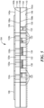
FIG. 1 shows a portion of an array antenna provided from a plurality of tripole antenna elements disposed on a triangular lattice; -
FIG. 2 shows a single antenna element unit cell of the array ofFIG. 1 ; -
FIG. 3 shows a bottom view of an antenna element ofFIG. 1 ; -
FIG. 4 is a transparent isometric view of the antenna element ofFIG. 3 ; -
FIG. 5 is a side view of the antenna element ofFIG. 3 ; and -
FIG. 6 is a cross-sectional view of an antenna element which may be the same as or substantially similar to the antenna element ofFIG. 3 coupled to a manifold. - Like reference symbols in the various drawings indicate like elements.
- Now referring to
FIG. 1 , an array antenna (or more simply "array") 100 includes a plurality of so called "tripole current loop"antenna elements 104a-104p. Each of theantenna elements 104a-104p are provided from threeconductors 106a-106c (also referred to herein as "arms") disposed in a predefined spaced relation on afirst surface 102a of asubstrate 102. In particular,conductors 106a-106c are disposed having a triangular relationship with respect to a center point. That is, each conductor or arm in an element is spaced apart and is rotated by an angle of about 120° with respect to the other conductors which comprise the element. - As illustrated in
Fig. 1 ,array 100 is provided having a triangular lattice. That is,antenna elements 104a-104p can be disposed onsubstrate 102 having a triangular lattice spacing (for clarity, atriangular grid 107 is superimposed over the example array illustrated inFIG. 1 ; it should be appreciated thatgrid 107 is not part of thearray 100, but rather is only included for clarity). As illustrated inFIG. 1 , each ofantenna elements 104a-104p are disposed at one of a plurality of vertices 111 (or nodes) oftriangular grid 107. Thus,antenna elements 104a-104p are disposed at various points along atriangular grid 107. - In the illustrative embodiment of
FIG. 1 , arms ofantenna elements line 109a and arms ofantenna elements line 109b. Further, and as noted above,conductors 106a-106c which make up each ofantenna elements 104a-104p, are disposed having a triangular relationship (i.e., 120° relationship) with respect to each other, and in the illustrative embodiment ofFIG. 1 , a center point between the three conductors is aligned with at least one of the plurality of vertices 111 (or node) oftriangular grid 107. -
Conductors 106a-106c may be provided from any electrical conductor (e.g., a metallic material) or any material electrically responsive to RF signals provided thereto.Conductors 106a-106c may be formed having the same or substantially same geometric shape. In other embodiments, one or more ofconductors 106a-106c may have different geometric shapes.Conductors 106a-106c may be formed in a variety of different shapes, including but not limited to any regular or irregular geometric shape. In some embodiments, the thickness (or width) ofconductors 106a-106c can be varied to modify (e.g., improve) design performance. The shape and/or properties ofconductors 106a-106c can be selected based, at least in part, on the dimensions ofarray antenna 100 and/or a particular application ofarray antenna 100. For example, the shape ofconductors 106a-106c can be modified to change a performance characteristic and/or frequency band within which therespective antenna element 104 orarray antenna 100 operates. Such performance characteristics include, but are not limited to, return and insertion loss, gain, and/or axial ratio characteristics therespective antenna element 104 orarray antenna 100. -
Substrate 102 comprises a dielectric material. In some embodiments,substrate 102 may include multiple layers some of which may be a dielectric material and some of which may be a non-dielectric material, as will be discussed in greater detail below with respect toFIGs. 2 and4-5 . - Referring now to
FIG. 2 , an array antenna unit cell 200 (hereinafter unit cell) includes threeconductors 106a-106c disposed on afirst surface 102a of asubstrate 102 so as to formantenna element 104 onfirst surface 102a ofsubstrate 102. It should be appreciated thatantenna element 104 may be the same as or substantially similar to at least one of the plurality ofantenna elements 104a-104p ofFIG. 1 . In the illustrative embodiment ofFIG. 2 ,unit cell 200 is provided having six (6) sides. Unit cells having other shapes, may of course, also be used. -
Unit cell 200 further includes aground plane 108 disposed on a second, oppositesurface 102b ofsubstrate 102. Asecond substrate 103 may be disposed over asecond surface 108b ofground plane 108. Each ofconductors 106a-106c is coupled toground 108 through a ground via as will be described in more detailed below with respect toFIG. 3 . - Thus,
array antenna 100 ofFIG. 1 may include a plurality of unit cells, each having antenna elements comprising threeconductors 106a-106c positioned such that they are disposed adjacent to each other and physically spaced apart in a center of the respective unit cell. -
Conductors 106a-106c are disposed onfirst surface 102a ofsubstrate 102 and spaced apart from each other. Thus, agap 105a-105c exists between each ofconductors 106a-106c such that theconductors 106a-106c are not in physical contact. -
Conductors 106a-106c can, for example, be spaced apart from each other and arranged alongfirst surface 102a so as to be responsive to radio frequency (RF) signals at a desired frequency range. In some embodiments, the spacing betweenconductors 106a-106c can be selected based at least in part on performance requirements and/or frequency band requirements of a particular application in which arespective antenna element 104 and/orarray antenna 100 is used. For example, changing the spacing (e.g., changing the gap) betweenconductors 106a-106c can change the return loss and insertion loss performance, gain, and/or axial ratio characteristics of arespective antenna element 104 and/orarray antenna 100. In some embodiments,antenna element 104 andconductors 106a-106c can be configured to be responsive to RF signals in the Q band frequency range (e.g., 33-50 GHZ). However, it should be appreciated thatantenna element 104 andconductors 106a-106c can be configured to be responsive to RF signals in a variety of different frequency ranges, based at least in part upon the needs of a particular application in whichantenna element 104 is used. - As illustrated in
FIG. 2 ,conductors 106a-106c are disposed having a triangular relationship (i.e., 120° relationship) with respect to each other. Such an arrangement allows a center point between the three conductors to be aligned at one of the plurality of vertices (or nodes) 111 (FIG. 1 ) of a triangular grid (e.g.,triangular grid 107 ofFIG. 1 ) so as to provide an array having a triangular lattice structure. In an embodiment, the use of threeconductors 106a-106c having a spaced triangular relationship provides for polarization alignment betweenconductors 106a-106c and a triangular lattice of an array antenna which may be formed by antenna elements provided fromconductors 106a-106c andsubstrate 102. The polarization alignment ofconductors 106a-106c can provide for a more predictable change over scan in mutual coupling between antenna elements in an array antenna, such as betweenantenna elements 104 ofarray antenna 100 ofFIG. 1 . The more predictable change over scan can provide an improved scan performance, particularly at far scan angles. - The use of three
conductors 106a-106c (instead of four as in traditional quad pole designs) reduces the footprint required byconductors 106a-106 withinunit cell 100 and facilitates inclusion of additional circuitry withinunit cell 200. Additionally, the use of the triangular lattice instead of a rectangular lattice provides a large unit cell area that is substantially grating lobe free, which also provides more space for feed circuitry and vertical vias. This additional area for circuitry can become very important at higher frequencies where a particular application of an antenna element or array antenna is required by grating lobe physics to be on a smaller lattice to maintain scan performance. For example,conductors 106a-106c can be sized and provided withinunit cell 200 with enough spacing to accommodate vertical transitions to active devices (not shown). The shape and triangular relationship between the three spaced conductors orarms 106a-106c which form the antenna element allows the antenna element to be used in an array having a triangular lattice. This, in turn, allows forfewer antenna elements 104a-104p to be used within an array antenna of a given size (area) as compared to a similarly sized array having a rectangular lattice structure. Such a decrease in the number of antenna elements maintains antenna gain while reducing overall array cost (because fewer active devices and components are required to support fewer channels, simplifying packaging of components on the array and reducing component cost). - Referring now to
FIGs. 3 and4 in which like elements are provided having like reference designations, each ofconductors 106a-106c include at least one signal via 120a-120c and at least one ground via 124a-124c to couple the respective conductors to afeed circuit 130 and a ground plane (e.g.,ground plane 108 ofFIG. 2 ) respectively. For example, a first signal via 120a and a first ground via 124a are coupled toconductor 106a. A second signal via 120b and a second ground via 124b are coupled toconductor 106b. A third signal via 120c and a third ground via 124c are coupled toconductor 106c. Thus, a tripole antenna element configured to generate circular polarizations can be provided having a single feed, here feedcircuit 130. -
Feed circuit 130 includes asignal path 132 coupled to first, second andthird antenna ports 121a-121c throughsignal paths paths Signal path 132 is coupled to port 131 (e.g., signal port interface) where a vertical RF via transition couples feedcircuit 130 to various circuit portions of which the respective antenna element is a part. For example, in one embodiment,port 131 couples feedcircuit 130 to active devices mounted on a printed wiring board (PWB). In some embodiments,signal path 132 may be referred to herein as a feed line. - A first end of first signal via 120a is coupled to
first conductor 106a and a second end of signal via is coupled to feedcircuit 130. In this way, RF signals may be coupled between the antenna element andport 131. Similarly, second signal via 120b has a first end coupled tosecond conductor 106b and a second end coupledfeed circuit 130 and third signal via 120c has a first end coupled tothird conductor 106c and a second end coupled to feedcircuit 130. Thus, feedcircuit 130 can provide RF signals to each of first, second andthird conductors 106a-106c. - The
feed circuit 130 is formed and configured to provide RF signals having equal amplitudes and phases shifted by 120° toconductors 106a-106c. For example,signal path 132 and each ofdelay lines feed circuit 130 provides RF signals to first, second andthird conductors 106a-106c respectively that are phase shifted 120° from RF signals provided to an adjacent (or neighboring) one of first, second andthird conductors 106a-106c. Thus, each of the arms may be excited from signals provided through the threesignal vias 120a-120c. - In this illustrative embodiment,
feed circuit 130 is provided from a pair of conductor signal layers (i.e. as a two-layer feed) which provides 0, 120 and 240 degree phase shifted equal amplitude signals toantenna element arms 106a-106c. -
Signal path 132 includes acoupling region 133 in whichpath 134 serves as a ground to signalpath 132.Coupling region 133 directs one-third of the power fed from a first end of signal path 132 (i.e. a port 131) toconductor 106b and two-thirds of the power propagates along path portion 132b towardconductors input port 131 is provided to conductor (or arm) 106c and one-third of the power is provided to conductor (or arm) 106a viasignal path 138. It should be appreciated thatpaths arms 106a-106c receive signals having an equal amount of signal power with relative phase shifts of 0°/120°/240° for right hand circuit polarization (RHCP). - As illustrated in
FIG. 3 , a first end offeed line 132 is configured to couple RF signals to and/or fromport 131, which, in turn, couples signals to and/or from various portions of an RF system of whichantenna element 104 is a part. For example,port 131 may be provided as an interface that couplesfeed circuit 130 to the various portions of an RF system (e.g., passive or active devices and/or circuits) through a vertical via transition. Thus,feed line 132 couples signals between the respective antenna ports and input/output port 131. -
Feed circuit 130 includes afirst delay line 134 coupling second signal via 120b to a second ground via 124b. Asecond delay line 136 couples third signal via 120c to a third ground via 124c, and athird delay line 138 couples third signal via 120c to first signal via 120a. -
Feed line 132 couples to third signal via 120c with third signal via 120c coupled to first signal via 120a throughthird delay line 138. Thus,feed line 132 can be configured to provide RF signals having a greater power factor to third signal via 120c as compared to the RF signal provided to second signal via 120b, as third signal via 120c is coupled to first signal via 120a and shares (e.g., splits) the RF signals with first signal via 120a. In one embodiment, a combined power factor of RF signals provided to third andfirst signal vias -
First delay line 134 andsecond delay line 136 can be spaced apart from each other a predetermined distance such that the predetermined distance produces a 120° phase shift between the RF signals provided to second signal via 120b and third signal via 120c. It should be appreciated that the predetermined distance betweenfirst delay line 134 andsecond delay line 136 can be selected to achieve a variety of different phase shifts. -
Third delay line 136 can be formed such that it splits RF signals between third signal via 120c and first signal via 120a. For example, a length, width (e.g., impedance) and/or shape (here an upside down L shape) ofthird delay line 138 can be selected such that it produces an approximately 120° phase shift between the RF signals provided to third signal via 120c and first signal via 120a. Thus, each of first, second andthird signal vias 120a-120c can be excited with RF signals approximately 120° out of phase relative to an adjacent signal via. - In some embodiments, first, second, and
third delay lines third delay lines third delay lines third delay lines FIG. 3 , the properties of first, second andthird delay lines conductors 106a-106c having equal amplitude but 120° out of phase relative to an adjacent one ofconductors 106a-106c. - It should be appreciated that shapes, impedances, lengths and/or spacing between first, second and
third delay lines - Each of
conductors 106a-106c is coupled to ground plane (e.g.,ground plane 108 ofFIG. 2 ) through at least one of ground vias 124a-124c. For example, and as illustrated inFIG. 3 , first ground via 124a couples a surface offirst conductor 106a to a ground plane, second ground via 124b couples a surface ofsecond conductor 106b to the ground plane, and third ground via 124c couples a surface ofthird conductor 106c to the ground plane. - A plurality of leakage vias 122a-122k can be formed in
antenna element 104 to prevent RF leakage through a feed layer, such as the feed layer betweenfeed circuit 130 andconductors 106a-106c. For example, and as will be described in greater detail with respect toFIGs. 4-5 ,leakage vias 122a-122k can be formed in a different layer ofantenna element 104 thanground vias 124a-124c and can form a cavity such that energy is transferred to (e.g., up to)conductors 106a-106c and doesn't leak through a stripline layer disposed adjacent to the feed layer ofantenna element 104. In the illustrative embodiment ofFIG. 3 ,leakage vias 122a-122k are formed generally in a circular shape, however it should be appreciated thatleakage vias 122a-122k can be formed in a variety of different shapes (e.g., rectangular, spherical, etc.) to prevent leakage. Further, the number of leakage vias 122a-122k can be selected based at least in part on a dimensions of a respective antenna element and its respective components and/or a frequency of RF signals being provided. For example, in an embodiment, the size of the cavity created byleakage vias 122a-122k can be used to tune the respective antenna element or array antenna. - Referring now to
FIG. 4 ,conductors 106a-106c are formed over afirst surface 140a of a firstdielectric region 140 forming anantenna circuit 150.Feed line 132 and first andsecond delay lines dielectric region 142 as part offeed circuit 130. In an embodiment, seconddielectric region 142 can be formed proximate to asecond surface 108b of ground plane 108 (here below ground plane 108) ofantenna element 104. Signals vias 120a-120c can be formed through firstdielectric region 140 and a portion of seconddielectric region 142 to couple a surface ofconductors 106a-106c to feedline 132. For example, in an embodiment,antenna circuit 150 is formed adjacent to afirst surface 108a of ground plane 108 (here above ground plane 108) andfeed circuit 130 is formed adjacent tosecond surface 108b of ground plane 108 (here below ground plane 108). - In the illustrative embodiment of
FIG. 4 , first signal via 120a extends fromfirst conductors 106a to afirst antenna port 121a, second signal via 120b extends fromsecond conductors 106b to asecond antenna port 121b, and third signal via 120c extends fromthird conductor 106c to a third antenna port 121c. In an embodiment, each of first, second andthird antenna ports 121a-121c can be part of the signal path forantenna element 104. For example, each of first, second andthird antenna ports 121a-121c can be coupled to feedline 132 to provide RF signals to first, second andthird signal vias 120a-120c, respectively. In some embodiments,first antenna port 121a can be coupled to thesecond region 138 ofsecond delay line 135 to receive RF signals,second port 121b can be coupled to thefirst delay line 134 to receive RF signals and third antenna port 121c can be capacitively coupled to feedline 132 to receive RF signals. In an embodiment, first, second andthird antenna ports 121a-121c may optionally include impedance tuning features (e.g., copper etched pads) added in some embodiments to improve loss performance. - As illustrated in
FIG. 4 ,ground vias 124a-124c are formed through firstdielectric region 140 to couple a surface ofconductors 106a-106c toground plane 108. Seconddielectric region 142 is belowsecond surface 108b ofground plane 108.Leakage vias 122a-122k can be formed within seconddielectric region 142. In some embodiments,leakage vias 122a-122k can be formed through seconddielectric region 142 such that they extend fromground plane 108 to an additional ground plane formed proximate to a second surface 142b of seconddielectric region 142. - For example, and referring now to
FIG. 5 , asecond ground plane 110 can be formed proximate to (here under) a second surface 142b of seconddielectric region 142. Further, and as illustrated inFIG. 5 ,leakage vias 122a-122k can be formed to couple a surface offirst ground plane 108 to a surface ofsecond ground plane 110. Thus,leakage vias 122a-122k can form a cavity proximate to (here under) couplings between signals vias 120a-120c canconductors 106a-106c to prevent leakage. - In the illustrative embodiment of
FIG .5 ,conductors 106a-106c are disposed proximate to afirst surface 140a of firstdielectric region 140.Signal vias 120a-120c extend from a surface ofconductors 106a-106c to feedline 132 anddelay lines dielectric region 140 and a portion of seconddielectric region 142. For example, signal vias 120a-c can extend through firstdielectric region 140 and a portion of seconddielectric region 142 to couple to components offeed circuit 130, described above. In some embodiments, one or more openings may be formed inground plane 108 such thatsignal vias 120a-120c can extend through and couple to delaylines -
Ground vias 124a-124c extend from a surface ofconductors 106a-106c toground plane 108. - Referring now to
FIG. 6 , a structure 600 having a manifold 602 coupled to anantenna element 604. In an embodiment,antenna element 604 may be the same as or substantially similar toantenna element 104 as described above with respect toFIGs. 1-5 . In some embodiments, structure 600 may include a printed wiring board (PWB) stack up havingmanifold 602 andantenna element 604 and power and control layers support active devices. - Manifold 600 may include circuitry operable to couple or otherwise convey an electrical signal (e.g., RF signal) to
antenna element 604 or an array antenna having a plurality ofantenna elements 604. - In the illustrative embodiment of
FIG. 6 ,antenna element 604 includesconductors 606 formed on afirst surface 640a of afirst layer 640.Conductors 606 are coupled to afirst ground plane 608 through one or more ground vias 624.Conductors 606 are coupled to afeed circuit 630 through one ormore signal vias 620. -
Ground plane 608 is generally disposed between firstdielectric region 640 and a second layer dielectric region 642 ofantenna element 604.Feed circuit 630 may include a feed line, one or more delay lines, a signal port and antenna ports to provide RF signals to conductors 660.Feed circuit 630 can be formed within second layer 642. One ormore leakage vias 622 can be formed such that they extend fromfirst ground plane 608 to asecond ground plane 610. In some embodiments,second ground plane 610 may be a component ofmanifold 602. In other embodiments,second ground plane 610 may be formed as a component ofantenna element 620. - Having described preferred embodiments, which serve to illustrate various concepts, structures and techniques, which are the subject of this patent, it will now become apparent that other embodiments incorporating these concepts, structures and techniques may be used. Accordingly, it is submitted that the scope of the patent should not be limited to the described embodiments but rather should be limited only by the scope of the following claims.
Claims (15)
- A radio frequency, RF, antenna element (104a-p) comprising:a substrate (102) having first (102a) and second opposing surfaces;three conductors (106a-c) disposed on the first surface of said substrate, said three conductors being physically spaced apart from each other and being arranged so as to form an antenna element responsive to RF signals at a desired frequency range;a feed circuit (130) having a signal port and first, second and third antenna ports (121a-c), each of the first, second and third antenna ports coupled to a respective one of the three conductors through a respective one of first, second, and third signal vias (120a-c); anda first ground via (124a) extending from a first conductor of the three conductors to a first ground plane (108), a second ground via (124b) extending from a second conductor of the three conductors to the first ground plane and a third ground via (124c) extending from a third conductor of the three conductors to the first ground plane;wherein said feed circuit is configured such that in response to an RF signal provided to the signal port thereof, said feed circuit provides at each of the first, second and third antenna ports, RF signals having equal amplitudes and phases shifted by 120 degrees.
- The antennal element of claim 1, wherein the three conductors have the same geometric shape.
- The antenna element of claim 1, further comprising a plurality of leakage vias disposed having a geometric relationship with respect to each other, each of the plurality of leakage vias coupling the first ground plane to a second ground plane.
- The antenna element of claim 3, wherein the antenna element comprises two layers such that the three conductors are disposed in a first layer and the plurality of leakage vias are disposed in a second layer.
- The antenna element of claim 1, wherein the feed circuit further comprises a feed line coupling the signal port to the second signal via, wherein the feed line is configured to provide the RF signals to each of the first, second and third signal vias having the equal amplitudes and having the 120 degree phase shift relative to the RF signals provided to an adjacent one of the first, second and third signal vias.
- The antenna element of claim 5, further comprising a first delay line having a first length, a second delay line having a second length, and a third delay line having a third length, wherein the first delay line couples the second ground via to the second signal via and the second delay line couples the third ground via to the third signal via and the third delay line couples the third signal via to the first signal via.
- The antenna element of claim 6, wherein:a portion of the feed line is disposed proximate to a portion of the first delay line to couple the feed line to the first delay line, and wherein the first delay line serves as a ground reference to the feed line; orthe first delay line and second delay line are spaced a predetermined distance from each other, and wherein the predetermined distance produces the 120 degree phase shift between the RF signals provided to the first and second signal vias; and optionally wherein the predetermined distance is selected such that a combined power factor of the RF signals provided to the second signal via and third signal via is two times greater than a power factor of the RF signals provided to the first signal via; orwherein the third length of the third delay line is selected to produce the 120 degree phase shift between the RF signals provided to the second signal via and third signal via.
- An array antenna comprising:a substrate having first and second opposing surfaces; anda plurality of antenna elements disposed on the first surface of said substrate, each of the plurality of antenna elements comprising:
three conductors physically spaced apart from each other and arranged so as to be responsive to RF signals at a desired frequency range;a feed circuit having a signal port and first, second and third antenna ports, each of the first, second and third antenna ports coupled to a respective one of the three conductors through a respective one of first, second, and third signal vias; anda first ground via extending from a first conductor of the three conductors to a first ground plane, a second ground via extending from a second conductor of the three conductors to the first ground plane and a third ground via extending from a third conductor of the three conductors to the first ground plane;wherein said feed circuit is configured such that in response to an RF signal provided to the signal port thereof, said feed circuit provides at each of the first, second and third antenna ports, RF signals having equal amplitudes and phases shifted by 120 degrees. - The array antenna of claim 8, wherein each of the antenna elements further comprises a plurality of leakage vias disposed having a geometric relationship with respect to each other, each of the plurality of leakage vias coupling the first ground plane to a second ground plane.
- The array antenna of claim 9, wherein each of the antenna elements further comprises two layers such that the three conductors are disposed in a first layer and the plurality of leakage vias are disposed in a second layer.
- The array antenna of claim 8, wherein each of the antenna elements further comprises a feed line coupling the signal port to the second signal via, wherein the feed line is configured to provide the RF signals to each of the first, second and third signal vias having the equal amplitudes and having the 120 degree phase shift relative to the RF signals provided to an adjacent one of the first, second and third signal vias.
- The array antenna of claim 11, wherein each of the antenna elements further comprises a first delay line having a first length, a second delay line having a second length and a third delay line having a third length, wherein the first delay line couples the second ground via to the second signal via, the second delay line couples the third ground via to the third signal via and the third delay line couples the third signal via to the first signal via.
- The array antenna of claim 12, wherein a portion of the feed line is disposed proximate to a portion of the first delay line to couple the feed line to the first delay line, and wherein the first delay serves as a ground reference to the feed line.
- The array antenna of claim 12, wherein the first delay line and second delay line are spaced a predetermined distance from each other, and wherein the predetermined distance produces the 120 degree phase shift between the RF signals provided to the first and second signal vias.
- The array antenna of claim 14, wherein the third length of the third delay line is selected to produce the 120 degree phase shift between the RF signals provided to the second signal via and third signal via.
Applications Claiming Priority (2)
| Application Number | Priority Date | Filing Date | Title |
|---|---|---|---|
| US15/731,906 US10361485B2 (en) | 2017-08-04 | 2017-08-04 | Tripole current loop radiating element with integrated circularly polarized feed |
| PCT/US2018/015421 WO2019027502A1 (en) | 2017-08-04 | 2018-01-26 | Tripole current loop radiating element with integrated circularly polarized feed |
Publications (2)
| Publication Number | Publication Date |
|---|---|
| EP3662537A1 EP3662537A1 (en) | 2020-06-10 |
| EP3662537B1 true EP3662537B1 (en) | 2024-10-09 |
Family
ID=61193091
Family Applications (1)
| Application Number | Title | Priority Date | Filing Date |
|---|---|---|---|
| EP18704713.9A Active EP3662537B1 (en) | 2017-08-04 | 2018-01-26 | Tripole current loop radiating element with integrated circularly polarized feed |
Country Status (4)
| Country | Link |
|---|---|
| US (1) | US10361485B2 (en) |
| EP (1) | EP3662537B1 (en) |
| KR (1) | KR102242123B1 (en) |
| WO (1) | WO2019027502A1 (en) |
Families Citing this family (9)
| Publication number | Priority date | Publication date | Assignee | Title |
|---|---|---|---|---|
| US10541461B2 (en) | 2016-12-16 | 2020-01-21 | Ratheon Company | Tile for an active electronically scanned array (AESA) |
| CA3077700A1 (en) * | 2017-10-19 | 2019-04-25 | Wafer, Llc | Polymer dispersed/shear aligned phase modulator device |
| US10879582B1 (en) * | 2019-08-12 | 2020-12-29 | Rockwell Collins, Inc. | Dielectric reinforced formed metal antenna |
| CN110797654B (en) * | 2019-12-03 | 2025-04-25 | 惠州硕贝德无线科技股份有限公司 | A high isolation antenna between the same frequency bands and a micro base station |
| US11152715B2 (en) | 2020-02-18 | 2021-10-19 | Raytheon Company | Dual differential radiator |
| EP4118707B1 (en) * | 2020-03-09 | 2026-01-07 | Nokia Technologies Oy | An antenna arrangement |
| FR3125886B1 (en) * | 2021-07-27 | 2023-11-24 | Commissariat Energie Atomique | Electromagnetic field probe |
| CN116454601A (en) * | 2023-03-14 | 2023-07-18 | 福耀玻璃工业集团股份有限公司 | Glass antenna, vehicle glass and vehicle |
| CN120691103A (en) * | 2024-03-20 | 2025-09-23 | 华为技术有限公司 | Antenna assembly and communication equipment |
Family Cites Families (156)
| Publication number | Priority date | Publication date | Assignee | Title |
|---|---|---|---|---|
| US2015028A (en) | 1932-04-12 | 1935-09-17 | Us Ind Alcohol Co | Holder for advertising material |
| US3414892A (en) | 1967-12-26 | 1968-12-03 | Lab For Electronics Inc | Means interconnecting printed circuit memory planes |
| US3528050A (en) | 1969-05-02 | 1970-09-08 | Holub Ind Inc | Push-on type grounding clip |
| US3624587A (en) | 1970-02-09 | 1971-11-30 | Litton Systems Inc | Clinched-wire interconnection device for printed circuit boards |
| US3960424A (en) | 1974-10-02 | 1976-06-01 | Amp Incorporated | Multi-contact spring connector for board to board connections |
| JPS6010297Y2 (en) | 1981-11-24 | 1985-04-09 | ソニー株式会社 | connector |
| FR2575336B1 (en) | 1984-12-21 | 1989-12-22 | Francelco Sa | CONNECTOR WITH NON-SLIDING CONTACTS |
| US4686536A (en) | 1985-08-15 | 1987-08-11 | Canadian Marconi Company | Crossed-drooping dipole antenna |
| US4690471A (en) | 1986-05-19 | 1987-09-01 | Motorola, Inc. | RF interconnect with triaxial self-alignment |
| US5060369A (en) | 1990-01-31 | 1991-10-29 | Ford Motor Company | Printed wiring board construction |
| JP2525545Y2 (en) | 1990-06-27 | 1997-02-12 | 日本電業工作株式会社 | Broadband microstrip antenna |
| US5146308A (en) | 1990-10-05 | 1992-09-08 | Micron Technology, Inc. | Semiconductor package utilizing edge connected semiconductor dice |
| US5172082A (en) | 1991-04-19 | 1992-12-15 | Hughes Aircraft Company | Multi-octave bandwidth balun |
| JPH0567912A (en) | 1991-04-24 | 1993-03-19 | Matsushita Electric Works Ltd | Flat antenna |
| FR2683952A1 (en) | 1991-11-14 | 1993-05-21 | Dassault Electronique | IMPROVED MICRO-TAPE ANTENNA DEVICE, PARTICULARLY FOR TELEPHONE TRANSMISSIONS BY SATELLITE. |
| US5244395A (en) | 1992-07-29 | 1993-09-14 | Motorola, Inc. | Circuit interconnect system |
| US5410281A (en) | 1993-03-09 | 1995-04-25 | Sierra Technologies, Inc. | Microwave high power combiner/divider |
| US5355283A (en) | 1993-04-14 | 1994-10-11 | Amkor Electronics, Inc. | Ball grid array with via interconnection |
| US5338207A (en) | 1993-06-09 | 1994-08-16 | The Whitaker Corporation | Multi-row right angle connectors |
| JPH07106841A (en) | 1993-10-06 | 1995-04-21 | Mitsubishi Electric Corp | Printed dipole antenna |
| US5434575A (en) | 1994-01-28 | 1995-07-18 | California Microwave, Inc. | Phased array antenna system using polarization phase shifting |
| US5455546A (en) | 1994-09-22 | 1995-10-03 | Glenayre Electronics, Inc. | High power radio frequency divider/combiner |
| US5644277A (en) | 1995-02-27 | 1997-07-01 | Hughes Aircraft Company | Three-wire-line vertical interconnect structure for multilevel substrates |
| US5661901A (en) | 1995-07-10 | 1997-09-02 | Micron Technology, Inc. | Method for mounting and electrically interconnecting semiconductor dice |
| US5603620A (en) | 1995-08-04 | 1997-02-18 | Delco Electronics Corp. | Integrated printed circuit connector and ground clip assembly |
| US6147648A (en) | 1996-04-03 | 2000-11-14 | Granholm; Johan | Dual polarization antenna array with very low cross polarization and low side lobes |
| US5938455A (en) | 1996-05-15 | 1999-08-17 | Ford Motor Company | Three-dimensional molded circuit board having interlocking connections |
| US6184832B1 (en) | 1996-05-17 | 2001-02-06 | Raytheon Company | Phased array antenna |
| US5745079A (en) * | 1996-06-28 | 1998-04-28 | Raytheon Company | Wide-band/dual-band stacked-disc radiators on stacked-dielectric posts phased array antenna |
| US5880694A (en) * | 1997-06-18 | 1999-03-09 | Hughes Electronics Corporation | Planar low profile, wideband, wide-scan phased array antenna using a stacked-disc radiator |
| US5886590A (en) | 1997-09-04 | 1999-03-23 | Hughes Electronics Corporation | Microstrip to coax vertical launcher using fuzz button and solderless interconnects |
| JPH11121896A (en) | 1997-10-16 | 1999-04-30 | Toshiba Corp | Circuit wiring board and method of manufacturing the same |
| JPH11145648A (en) | 1997-11-12 | 1999-05-28 | Harness Syst Tech Res Ltd | Method of fixing electronic components to printed circuit board and printed circuit board |
| US6114221A (en) | 1998-03-16 | 2000-09-05 | International Business Machines Corporation | Method and apparatus for interconnecting multiple circuit chips |
| US6114997A (en) | 1998-05-27 | 2000-09-05 | Raytheon Company | Low-profile, integrated radiator tiles for wideband, dual-linear and circular-polarized phased array applications |
| JP2000312112A (en) | 1998-09-22 | 2000-11-07 | Matsushita Electric Ind Co Ltd | Patch antenna device |
| US6320542B1 (en) | 1998-09-22 | 2001-11-20 | Matsushita Electric Industrial Co., Ltd. | Patch antenna apparatus with improved projection area |
| US6100775A (en) | 1998-10-15 | 2000-08-08 | Raytheon Company | Vertical interconnect circuit for coplanar waveguides |
| US6307160B1 (en) | 1998-10-29 | 2001-10-23 | Agilent Technologies, Inc. | High-strength solder interconnect for copper/electroless nickel/immersion gold metallization solder pad and method |
| US6351133B1 (en) | 1999-03-31 | 2002-02-26 | Adoamtest Corp. | Packaging and interconnection of contact structure |
| JP3306592B2 (en) | 1999-05-21 | 2002-07-24 | 株式会社豊田中央研究所 | Microstrip array antenna |
| US6830460B1 (en) | 1999-08-02 | 2004-12-14 | Gryphics, Inc. | Controlled compliance fine pitch interconnect |
| US6166701A (en) | 1999-08-05 | 2000-12-26 | Raytheon Company | Dual polarization antenna array with radiating slots and notch dipole elements sharing a common aperture |
| WO2002023672A2 (en) | 2000-09-15 | 2002-03-21 | Raytheon Company | Microelectromechanical phased array antenna |
| JP3826696B2 (en) | 2000-09-19 | 2006-09-27 | 日産自動車株式会社 | Wiring structure |
| US6512487B1 (en) | 2000-10-31 | 2003-01-28 | Harris Corporation | Wideband phased array antenna and associated methods |
| US6602078B2 (en) | 2001-03-16 | 2003-08-05 | Cenix, Inc. | Electrical interconnect having a multi-layer circuit board structure and including a conductive spacer for impedance matching |
| US6429816B1 (en) | 2001-05-04 | 2002-08-06 | Harris Corporation | Spatially orthogonal signal distribution and support architecture for multi-beam phased array antenna |
| US6459415B1 (en) | 2001-05-14 | 2002-10-01 | Eleven Engineering Inc. | Omni-directional planar antenna design |
| US6580402B2 (en) | 2001-07-26 | 2003-06-17 | The Boeing Company | Antenna integrated ceramic chip carrier for a phased array antenna |
| US6867742B1 (en) | 2001-09-04 | 2005-03-15 | Raytheon Company | Balun and groundplanes for decade band tapered slot antenna, and method of making same |
| US20030112200A1 (en) | 2001-12-17 | 2003-06-19 | Alcatel, Radio Frequency Systems, Inc. | Horizontally polarized printed circuit antenna array |
| US6935866B2 (en) | 2002-04-02 | 2005-08-30 | Adc Telecommunications, Inc. | Card edge coaxial connector |
| US6882247B2 (en) | 2002-05-15 | 2005-04-19 | Raytheon Company | RF filtered DC interconnect |
| US6664867B1 (en) | 2002-07-19 | 2003-12-16 | Paratek Microwave, Inc. | Tunable electromagnetic transmission structure for effecting coupling of electromagnetic signals |
| US6686885B1 (en) | 2002-08-09 | 2004-02-03 | Northrop Grumman Corporation | Phased array antenna for space based radar |
| US6950062B1 (en) | 2002-10-18 | 2005-09-27 | Rockwell Collins | Method and structure for phased array antenna interconnect using an array of substrate slats |
| US6822617B1 (en) | 2002-10-18 | 2004-11-23 | Rockwell Collins | Construction approach for an EMXT-based phased array antenna |
| WO2004040696A1 (en) | 2002-10-24 | 2004-05-13 | Centre National De La Recherche Scientifique (C.N.R.S.) | Multibeam antenna with photonic bandgap material |
| US6891511B1 (en) | 2002-11-07 | 2005-05-10 | Lockheed Martin Corporation | Method of fabricating a radar array |
| US6975267B2 (en) | 2003-02-05 | 2005-12-13 | Northrop Grumman Corporation | Low profile active electronically scanned antenna (AESA) for Ka-band radar systems |
| US7230339B2 (en) | 2003-03-28 | 2007-06-12 | Intel Corporation | Copper ring solder mask defined ball grid array pad |
| JP4004048B2 (en) | 2003-04-11 | 2007-11-07 | Tdk株式会社 | High frequency transmission line |
| US7180457B2 (en) | 2003-07-11 | 2007-02-20 | Raytheon Company | Wideband phased array radiator |
| ATE396516T1 (en) | 2003-07-25 | 2008-06-15 | Stichting Astron | DOUBLE POLARIZED ANTENNA ARRANGEMENT AND PROCESS FOR PRODUCTION THEREOF |
| US6876336B2 (en) | 2003-08-04 | 2005-04-05 | Harris Corporation | Phased array antenna with edge elements and associated methods |
| US6856297B1 (en) | 2003-08-04 | 2005-02-15 | Harris Corporation | Phased array antenna with discrete capacitive coupling and associated methods |
| US7074047B2 (en) | 2003-11-05 | 2006-07-11 | Tensolite Company | Zero insertion force high frequency connector |
| US7315288B2 (en) | 2004-01-15 | 2008-01-01 | Raytheon Company | Antenna arrays using long slot apertures and balanced feeds |
| US6977623B2 (en) | 2004-02-17 | 2005-12-20 | Harris Corporation | Wideband slotted phased array antenna and associated methods |
| US7272880B1 (en) | 2004-05-27 | 2007-09-25 | Lockheed Martin Corporation | Distributed load edge clamp |
| WO2005119765A2 (en) | 2004-06-02 | 2005-12-15 | Tessera, Inc. | Assembly including vertical and horizontal joined circuit panels |
| US7012572B1 (en) | 2004-07-16 | 2006-03-14 | Hrl Laboratories, Llc | Integrated ultra wideband element card for array antennas |
| US7113142B2 (en) | 2004-10-21 | 2006-09-26 | The Boeing Company | Design and fabrication methodology for a phased array antenna with integrated feed structure-conformal load-bearing concept |
| US7109942B2 (en) | 2004-10-21 | 2006-09-19 | The Boeing Company | Structurally integrated phased array antenna aperture design and fabrication method |
| US7138952B2 (en) | 2005-01-11 | 2006-11-21 | Raytheon Company | Array antenna with dual polarization and method |
| US7084827B1 (en) | 2005-02-07 | 2006-08-01 | Harris Corporation | Phased array antenna with an impedance matching layer and associated methods |
| US8035992B2 (en) | 2005-10-18 | 2011-10-11 | Nec Corporation | Vertical transitions, printed circuit boards therewith and semiconductor packages with the printed circuit boards and semiconductor chip |
| US7358921B2 (en) | 2005-12-01 | 2008-04-15 | Harris Corporation | Dual polarization antenna and associated methods |
| US7221322B1 (en) | 2005-12-14 | 2007-05-22 | Harris Corporation | Dual polarization antenna array with inter-element coupling and associated methods |
| US7338292B2 (en) | 2006-01-26 | 2008-03-04 | Agilent Technologies, Inc. | Board-to-board electronic interface using hemi-ellipsoidal surface features |
| US7411472B1 (en) | 2006-02-01 | 2008-08-12 | Rockwell Collins, Inc. | Low-loss integrated waveguide feed for wafer-scale heterogeneous layered active electronically scanned array |
| US7444736B1 (en) | 2006-04-27 | 2008-11-04 | Lockheed Martin Corporation | Method for fabricating horn antenna |
| US8373597B2 (en) | 2006-08-09 | 2013-02-12 | Spx Corporation | High-power-capable circularly polarized patch antenna apparatus and method |
| US9019166B2 (en) | 2009-06-15 | 2015-04-28 | Raytheon Company | Active electronically scanned array (AESA) card |
| US9172145B2 (en) | 2006-09-21 | 2015-10-27 | Raytheon Company | Transmit/receive daughter card with integral circulator |
| US7708569B2 (en) | 2006-10-30 | 2010-05-04 | Fci Americas Technology, Inc. | Broadside-coupled signal pair configurations for electrical connectors |
| US7489283B2 (en) | 2006-12-22 | 2009-02-10 | The Boeing Company | Phased array antenna apparatus and methods of manufacture |
| US20080169992A1 (en) | 2007-01-16 | 2008-07-17 | Harris Corporation | Dual-polarization, slot-mode antenna and associated methods |
| EP1970952A3 (en) | 2007-03-13 | 2009-05-06 | Semiconductor Energy Laboratory Co., Ltd. | Semiconductor device and manufacturing method thereof |
| US7948441B2 (en) | 2007-04-12 | 2011-05-24 | Raytheon Company | Low profile antenna |
| US7675466B2 (en) | 2007-07-02 | 2010-03-09 | International Business Machines Corporation | Antenna array feed line structures for millimeter wave applications |
| US7688265B2 (en) | 2007-09-18 | 2010-03-30 | Raytheon Company | Dual polarized low profile antenna |
| US7579997B2 (en) | 2007-10-03 | 2009-08-25 | The Boeing Company | Advanced antenna integrated printed wiring board with metallic waveguide plate |
| US8031126B2 (en) | 2007-11-13 | 2011-10-04 | Raytheon Company | Dual polarized antenna |
| GB0724684D0 (en) | 2007-12-18 | 2009-01-07 | Bae Systems Plc | Anntenna Feed Module |
| US7766665B2 (en) | 2008-01-31 | 2010-08-03 | Ivus Industries, Inc. | Printed circuit board direct connection and method of forming the same |
| FR2928066A1 (en) | 2008-02-27 | 2009-08-28 | Thomson Licensing Sas | SYSTEM FOR INTERCONNECTING TWO SUBSTRATES COMPRISING EACH AT LEAST ONE TRANSMISSION LINE |
| US8044861B2 (en) | 2008-06-30 | 2011-10-25 | Harris Corporation | Electronic device with edge surface antenna elements and related methods |
| IT1391192B1 (en) | 2008-08-05 | 2011-11-18 | Selex Communications Spa | MULTILAYER STRUCTURE DEVICE WITH A VERTICAL TRANSITION BETWEEN A MICRO STRIP AND A STRIPLINE |
| NL1035878C (en) | 2008-08-28 | 2010-03-11 | Thales Nederland Bv | An array antenna comprising means to establish galvanic contacts between its radiator elements while allowing for their thermal expansion. |
| CN201562831U (en) | 2008-09-09 | 2010-08-25 | 莫列斯公司 | Connector with impedance tuning terminal arrangement |
| US7891980B2 (en) | 2008-11-05 | 2011-02-22 | Dialogic Corporation | Interconnect device with discrete in-line components |
| US8706049B2 (en) | 2008-12-31 | 2014-04-22 | Intel Corporation | Platform integrated phased array transmit/receive module |
| US20100186997A1 (en) | 2009-01-29 | 2010-07-29 | Samtec Inc. | Crimped solder on a flexible circuit board |
| WO2010096567A1 (en) | 2009-02-18 | 2010-08-26 | Molex Incorporated | Vertical connector for a printed circuit board |
| IL197906A (en) | 2009-04-05 | 2014-09-30 | Elta Systems Ltd | Phased array antennas and method for producing them |
| US8325093B2 (en) | 2009-07-31 | 2012-12-04 | University Of Massachusetts | Planar ultrawideband modular antenna array |
| US20110089531A1 (en) | 2009-10-16 | 2011-04-21 | Teledyne Scientific & Imaging, Llc | Interposer Based Monolithic Microwave Integrate Circuit (iMMIC) |
| DE112010002548A5 (en) | 2009-12-17 | 2012-08-23 | Conti Temic Microelectronic Gmbh | CIRCUIT BOARD WITH MULTIPLE COUPLED PLATE LAYERS WITH A BARE-DIE MOUNTING FOR OPERATION AS A GEARBOX CONTROLLER |
| US8659499B1 (en) | 2010-01-15 | 2014-02-25 | Lockheed Martin Corporation | Fastener-less joint for radar array |
| KR20120035394A (en) | 2010-10-05 | 2012-04-16 | 삼성전자주식회사 | Apparatus for system-on-package using vertical transmission line transition and land grid array connection |
| US8542151B2 (en) | 2010-10-21 | 2013-09-24 | Mediatek Inc. | Antenna module and antenna unit thereof |
| US8928544B2 (en) | 2011-02-21 | 2015-01-06 | Her Majesty The Queen In Right Of Canada As Represented By The Minister Of National Defence | Wideband circularly polarized hybrid dielectric resonator antenna |
| US20120212920A1 (en) | 2011-02-21 | 2012-08-23 | Lockheed Martin Corporation | Circuit card assemblies having connector-less perpendicular card-to-card interconnects |
| US9112262B2 (en) | 2011-06-02 | 2015-08-18 | Brigham Young University | Planar array feed for satellite communications |
| WO2012167283A2 (en) | 2011-06-02 | 2012-12-06 | Brigham Young University | Planar array feed for satellite communications |
| TW201301964A (en) | 2011-06-30 | 2013-01-01 | Hon Hai Prec Ind Co Ltd | PWB connecting assembly |
| US20130026586A1 (en) | 2011-07-26 | 2013-01-31 | Texas Instruments Incorporated | Cross-loop antenna |
| US9373881B2 (en) | 2011-08-12 | 2016-06-21 | Bae Systems Information And Electronic Systems Integration Inc. | Low radar cross section array panel |
| US8786515B2 (en) | 2011-08-30 | 2014-07-22 | Harris Corporation | Phased array antenna module and method of making same |
| JP5822182B2 (en) | 2011-09-12 | 2015-11-24 | 日本精機株式会社 | Vehicle display device |
| TWI449475B (en) | 2012-01-09 | 2014-08-11 | Novatek Microelectronics Corp | Printed circuit board |
| US8648454B2 (en) | 2012-02-14 | 2014-02-11 | International Business Machines Corporation | Wafer-scale package structures with integrated antennas |
| US8780561B2 (en) | 2012-03-30 | 2014-07-15 | Raytheon Company | Conduction cooling of multi-channel flip chip based panel array circuits |
| US9054410B2 (en) | 2012-05-24 | 2015-06-09 | Commscope Technologies Llc | Dipole strength clip |
| US20130335931A1 (en) | 2012-06-15 | 2013-12-19 | Delphi Technologies, Inc. | Surface mount interconnection system for modular circuit board and method |
| JP5871729B2 (en) | 2012-06-28 | 2016-03-01 | 日本航空電子工業株式会社 | Housingless connector |
| US9077083B1 (en) | 2012-08-01 | 2015-07-07 | Ball Aerospace & Technologies Corp. | Dual-polarized array antenna |
| US9236652B2 (en) | 2012-08-21 | 2016-01-12 | Raytheon Company | Broadband array antenna enhancement with spatially engineered dielectrics |
| US9059517B2 (en) | 2012-09-04 | 2015-06-16 | The Boeing Company | Systems and methods for assembling conformal arrays |
| US9537208B2 (en) | 2012-11-12 | 2017-01-03 | Raytheon Company | Dual polarization current loop radiator with integrated balun |
| US9287632B2 (en) | 2012-11-30 | 2016-03-15 | The Boeing Company | Structural wideband multifunctional apertures |
| US20140160681A1 (en) | 2012-12-07 | 2014-06-12 | Wintec Industries, Inc. | Discrete-Pin Printed-Circuit Mounting with Notches |
| US8952752B1 (en) | 2012-12-12 | 2015-02-10 | Nuvotronics, Llc | Smart power combiner |
| US10403511B2 (en) | 2013-01-14 | 2019-09-03 | Intel Corporation | Backside redistribution layer patch antenna |
| US8921992B2 (en) | 2013-03-14 | 2014-12-30 | Raytheon Company | Stacked wafer with coolant channels |
| US9343816B2 (en) | 2013-04-09 | 2016-05-17 | Raytheon Company | Array antenna and related techniques |
| WO2015006293A1 (en) | 2013-07-08 | 2015-01-15 | Qualcomm Incorporated | Techniques for operating phased array antennas in millimeter-wave radio modules |
| US9136572B2 (en) | 2013-07-26 | 2015-09-15 | Raytheon Company | Dual stripline tile circulator utilizing thick film post-fired substrate stacking |
| US9190727B1 (en) | 2013-10-01 | 2015-11-17 | The Boeing Company | Structural wideband multifunctional aperture manufacturing |
| US10516214B2 (en) | 2013-11-05 | 2019-12-24 | Si2 Technologies, Inc. | Antenna elements and array |
| US9437929B2 (en) | 2014-01-15 | 2016-09-06 | Raytheon Company | Dual polarized array antenna with modular multi-balun board and associated methods |
| US9472859B2 (en) | 2014-05-20 | 2016-10-18 | International Business Machines Corporation | Integration of area efficient antennas for phased array or wafer scale array antenna applications |
| TWI677963B (en) | 2014-06-18 | 2019-11-21 | 愛爾蘭商艾克斯瑟樂普林特有限公司 | Micro assembled high frequency devices and arrays |
| US9402301B2 (en) | 2014-12-10 | 2016-07-26 | Raytheon Company | Vertical radio frequency module |
| US9660333B2 (en) | 2014-12-22 | 2017-05-23 | Raytheon Company | Radiator, solderless interconnect thereof and grounding element thereof |
| EP3262711B1 (en) | 2015-02-26 | 2020-11-18 | The Government of the United States of America as represented by the Secretary of the Navy | Planar ultrawideband modular antenna array having improved bandwidth |
| US9490519B2 (en) | 2015-03-19 | 2016-11-08 | James D Lilly | Transmission line transformer antenna |
| CN204857954U (en) | 2015-08-06 | 2015-12-09 | 中国电子科技集团公司第三十八研究所 | A Ka-band wide-angle scanning phased array antenna |
| US9780458B2 (en) | 2015-10-13 | 2017-10-03 | Raytheon Company | Methods and apparatus for antenna having dual polarized radiating elements with enhanced heat dissipation |
| EP3378123A4 (en) | 2015-11-17 | 2019-06-19 | Gapwaves AB | AUTOMATICALLY GROUND SINGLE BUTTERFLY ANTENNA ARRAY ARRANGEMENT, ANTENNA PEDAL AND METHOD OF MANUFACTURE |
| US9806432B2 (en) * | 2015-12-02 | 2017-10-31 | Raytheon Company | Dual-polarized wideband radiator with single-plane stripline feed |
| US10490907B2 (en) | 2016-09-27 | 2019-11-26 | Google Llc | Suppression of surface waves in printed circuit board-based phased-array antennas |
| US10541461B2 (en) | 2016-12-16 | 2020-01-21 | Ratheon Company | Tile for an active electronically scanned array (AESA) |
| US10658762B2 (en) * | 2017-07-14 | 2020-05-19 | Apple Inc. | Multi-band millimeter wave antenna arrays |
-
2017
- 2017-08-04 US US15/731,906 patent/US10361485B2/en active Active
-
2018
- 2018-01-26 EP EP18704713.9A patent/EP3662537B1/en active Active
- 2018-01-26 WO PCT/US2018/015421 patent/WO2019027502A1/en not_active Ceased
- 2018-01-26 KR KR1020197038981A patent/KR102242123B1/en active Active
Also Published As
| Publication number | Publication date |
|---|---|
| WO2019027502A1 (en) | 2019-02-07 |
| US20190044234A1 (en) | 2019-02-07 |
| EP3662537A1 (en) | 2020-06-10 |
| KR102242123B1 (en) | 2021-04-19 |
| US10361485B2 (en) | 2019-07-23 |
| KR20200011500A (en) | 2020-02-03 |
Similar Documents
| Publication | Publication Date | Title |
|---|---|---|
| EP3662537B1 (en) | Tripole current loop radiating element with integrated circularly polarized feed | |
| US8063832B1 (en) | Dual-feed series microstrip patch array | |
| Klionovski et al. | A dual-polarization-switched beam patch antenna array for millimeter-wave applications | |
| US5786793A (en) | Compact antenna for circular polarization | |
| US9000996B2 (en) | Modular wideband antenna array | |
| US8350774B2 (en) | Double balun dipole | |
| US20090140943A1 (en) | Slot antenna for mm-wave signals | |
| US20110090129A1 (en) | Circularly Polarised Array Antenna | |
| US10854996B2 (en) | Dual-polarized substrate-integrated beam steering antenna | |
| US6445346B2 (en) | Planar polarizer feed network for a dual circular polarized antenna array | |
| US10333228B2 (en) | Low coupling 2×2 MIMO array | |
| IL160629A (en) | Patch fed printed antenna | |
| CN112467395A (en) | Miniaturized low-profile dual-circularly-polarized antenna | |
| CN110676567A (en) | Double-circular-polarization patch array antenna based on broadband balun feed | |
| US4740793A (en) | Antenna elements and arrays | |
| WO2025036025A1 (en) | Circularly polarized antenna, array antenna, and communication device | |
| US10186768B2 (en) | Dipole antenna array | |
| Talbi et al. | A compact 4× 4 butler matrix for UWB applications | |
| US4660047A (en) | Microstrip antenna with resonator feed | |
| US11394114B2 (en) | Dual-polarized substrate-integrated 360° beam steering antenna | |
| Zhao et al. | A cross dipole antenna array in LTCC for satellite communication | |
| CN112271439A (en) | A circularly polarized microstrip antenna | |
| GB2510144A (en) | Dipole antenna array including at least one co-planar sub-array | |
| CN120016140B (en) | Ultra-wideband RCS (radio frequency control) reduced circular polarization antenna based on polarization conversion ultra-surface | |
| US20250357977A1 (en) | Antenna device, antenna device with multi-layer structure and wireless communication device |
Legal Events
| Date | Code | Title | Description |
|---|---|---|---|
| STAA | Information on the status of an ep patent application or granted ep patent |
Free format text: STATUS: UNKNOWN |
|
| STAA | Information on the status of an ep patent application or granted ep patent |
Free format text: STATUS: THE INTERNATIONAL PUBLICATION HAS BEEN MADE |
|
| PUAI | Public reference made under article 153(3) epc to a published international application that has entered the european phase |
Free format text: ORIGINAL CODE: 0009012 |
|
| STAA | Information on the status of an ep patent application or granted ep patent |
Free format text: STATUS: REQUEST FOR EXAMINATION WAS MADE |
|
| 17P | Request for examination filed |
Effective date: 20191209 |
|
| AK | Designated contracting states |
Kind code of ref document: A1 Designated state(s): AL AT BE BG CH CY CZ DE DK EE ES FI FR GB GR HR HU IE IS IT LI LT LU LV MC MK MT NL NO PL PT RO RS SE SI SK SM TR |
|
| AX | Request for extension of the european patent |
Extension state: BA ME |
|
| DAV | Request for validation of the european patent (deleted) | ||
| DAX | Request for extension of the european patent (deleted) | ||
| STAA | Information on the status of an ep patent application or granted ep patent |
Free format text: STATUS: EXAMINATION IS IN PROGRESS |
|
| 17Q | First examination report despatched |
Effective date: 20210909 |
|
| GRAP | Despatch of communication of intention to grant a patent |
Free format text: ORIGINAL CODE: EPIDOSNIGR1 |
|
| STAA | Information on the status of an ep patent application or granted ep patent |
Free format text: STATUS: GRANT OF PATENT IS INTENDED |
|
| GRAJ | Information related to disapproval of communication of intention to grant by the applicant or resumption of examination proceedings by the epo deleted |
Free format text: ORIGINAL CODE: EPIDOSDIGR1 |
|
| STAA | Information on the status of an ep patent application or granted ep patent |
Free format text: STATUS: EXAMINATION IS IN PROGRESS |
|
| INTG | Intention to grant announced |
Effective date: 20240516 |
|
| GRAP | Despatch of communication of intention to grant a patent |
Free format text: ORIGINAL CODE: EPIDOSNIGR1 |
|
| STAA | Information on the status of an ep patent application or granted ep patent |
Free format text: STATUS: GRANT OF PATENT IS INTENDED |
|
| INTC | Intention to grant announced (deleted) | ||
| INTG | Intention to grant announced |
Effective date: 20240625 |
|
| GRAS | Grant fee paid |
Free format text: ORIGINAL CODE: EPIDOSNIGR3 |
|
| GRAA | (expected) grant |
Free format text: ORIGINAL CODE: 0009210 |
|
| STAA | Information on the status of an ep patent application or granted ep patent |
Free format text: STATUS: THE PATENT HAS BEEN GRANTED |
|
| AK | Designated contracting states |
Kind code of ref document: B1 Designated state(s): AL AT BE BG CH CY CZ DE DK EE ES FI FR GB GR HR HU IE IS IT LI LT LU LV MC MK MT NL NO PL PT RO RS SE SI SK SM TR |
|
| REG | Reference to a national code |
Ref country code: CH Ref legal event code: EP |
|
| REG | Reference to a national code |
Ref country code: DE Ref legal event code: R096 Ref document number: 602018075143 Country of ref document: DE |
|
| REG | Reference to a national code |
Ref country code: IE Ref legal event code: FG4D |
|
| REG | Reference to a national code |
Ref country code: LT Ref legal event code: MG9D |
|
| REG | Reference to a national code |
Ref country code: NL Ref legal event code: MP Effective date: 20241009 |
|
| REG | Reference to a national code |
Ref country code: AT Ref legal event code: MK05 Ref document number: 1731632 Country of ref document: AT Kind code of ref document: T Effective date: 20241009 |
|
| PG25 | Lapsed in a contracting state [announced via postgrant information from national office to epo] |
Ref country code: NL Free format text: LAPSE BECAUSE OF FAILURE TO SUBMIT A TRANSLATION OF THE DESCRIPTION OR TO PAY THE FEE WITHIN THE PRESCRIBED TIME-LIMIT Effective date: 20241009 |
|
| PG25 | Lapsed in a contracting state [announced via postgrant information from national office to epo] |
Ref country code: NL Free format text: LAPSE BECAUSE OF FAILURE TO SUBMIT A TRANSLATION OF THE DESCRIPTION OR TO PAY THE FEE WITHIN THE PRESCRIBED TIME-LIMIT Effective date: 20241009 |
|
| PG25 | Lapsed in a contracting state [announced via postgrant information from national office to epo] |
Ref country code: HR Free format text: LAPSE BECAUSE OF FAILURE TO SUBMIT A TRANSLATION OF THE DESCRIPTION OR TO PAY THE FEE WITHIN THE PRESCRIBED TIME-LIMIT Effective date: 20241009 Ref country code: PT Free format text: LAPSE BECAUSE OF FAILURE TO SUBMIT A TRANSLATION OF THE DESCRIPTION OR TO PAY THE FEE WITHIN THE PRESCRIBED TIME-LIMIT Effective date: 20250210 Ref country code: IS Free format text: LAPSE BECAUSE OF FAILURE TO SUBMIT A TRANSLATION OF THE DESCRIPTION OR TO PAY THE FEE WITHIN THE PRESCRIBED TIME-LIMIT Effective date: 20250209 |
|
| PGFP | Annual fee paid to national office [announced via postgrant information from national office to epo] |
Ref country code: DE Payment date: 20241218 Year of fee payment: 8 |
|
| PG25 | Lapsed in a contracting state [announced via postgrant information from national office to epo] |
Ref country code: FI Free format text: LAPSE BECAUSE OF FAILURE TO SUBMIT A TRANSLATION OF THE DESCRIPTION OR TO PAY THE FEE WITHIN THE PRESCRIBED TIME-LIMIT Effective date: 20241009 |
|
| PG25 | Lapsed in a contracting state [announced via postgrant information from national office to epo] |
Ref country code: BG Free format text: LAPSE BECAUSE OF FAILURE TO SUBMIT A TRANSLATION OF THE DESCRIPTION OR TO PAY THE FEE WITHIN THE PRESCRIBED TIME-LIMIT Effective date: 20241009 |
|
| PG25 | Lapsed in a contracting state [announced via postgrant information from national office to epo] |
Ref country code: ES Free format text: LAPSE BECAUSE OF FAILURE TO SUBMIT A TRANSLATION OF THE DESCRIPTION OR TO PAY THE FEE WITHIN THE PRESCRIBED TIME-LIMIT Effective date: 20241009 |
|
| PG25 | Lapsed in a contracting state [announced via postgrant information from national office to epo] |
Ref country code: NO Free format text: LAPSE BECAUSE OF FAILURE TO SUBMIT A TRANSLATION OF THE DESCRIPTION OR TO PAY THE FEE WITHIN THE PRESCRIBED TIME-LIMIT Effective date: 20250109 |
|
| PG25 | Lapsed in a contracting state [announced via postgrant information from national office to epo] |
Ref country code: GR Free format text: LAPSE BECAUSE OF FAILURE TO SUBMIT A TRANSLATION OF THE DESCRIPTION OR TO PAY THE FEE WITHIN THE PRESCRIBED TIME-LIMIT Effective date: 20250110 Ref country code: LV Free format text: LAPSE BECAUSE OF FAILURE TO SUBMIT A TRANSLATION OF THE DESCRIPTION OR TO PAY THE FEE WITHIN THE PRESCRIBED TIME-LIMIT Effective date: 20241009 Ref country code: AT Free format text: LAPSE BECAUSE OF FAILURE TO SUBMIT A TRANSLATION OF THE DESCRIPTION OR TO PAY THE FEE WITHIN THE PRESCRIBED TIME-LIMIT Effective date: 20241009 |
|
| PG25 | Lapsed in a contracting state [announced via postgrant information from national office to epo] |
Ref country code: PL Free format text: LAPSE BECAUSE OF FAILURE TO SUBMIT A TRANSLATION OF THE DESCRIPTION OR TO PAY THE FEE WITHIN THE PRESCRIBED TIME-LIMIT Effective date: 20241009 |
|
| PG25 | Lapsed in a contracting state [announced via postgrant information from national office to epo] |
Ref country code: RS Free format text: LAPSE BECAUSE OF FAILURE TO SUBMIT A TRANSLATION OF THE DESCRIPTION OR TO PAY THE FEE WITHIN THE PRESCRIBED TIME-LIMIT Effective date: 20250109 |
|
| PG25 | Lapsed in a contracting state [announced via postgrant information from national office to epo] |
Ref country code: SM Free format text: LAPSE BECAUSE OF FAILURE TO SUBMIT A TRANSLATION OF THE DESCRIPTION OR TO PAY THE FEE WITHIN THE PRESCRIBED TIME-LIMIT Effective date: 20241009 |
|
| PG25 | Lapsed in a contracting state [announced via postgrant information from national office to epo] |
Ref country code: DK Free format text: LAPSE BECAUSE OF FAILURE TO SUBMIT A TRANSLATION OF THE DESCRIPTION OR TO PAY THE FEE WITHIN THE PRESCRIBED TIME-LIMIT Effective date: 20241009 |
|
| REG | Reference to a national code |
Ref country code: DE Ref legal event code: R097 Ref document number: 602018075143 Country of ref document: DE |
|
| PG25 | Lapsed in a contracting state [announced via postgrant information from national office to epo] |
Ref country code: EE Free format text: LAPSE BECAUSE OF FAILURE TO SUBMIT A TRANSLATION OF THE DESCRIPTION OR TO PAY THE FEE WITHIN THE PRESCRIBED TIME-LIMIT Effective date: 20241009 |
|
| PG25 | Lapsed in a contracting state [announced via postgrant information from national office to epo] |
Ref country code: RO Free format text: LAPSE BECAUSE OF FAILURE TO SUBMIT A TRANSLATION OF THE DESCRIPTION OR TO PAY THE FEE WITHIN THE PRESCRIBED TIME-LIMIT Effective date: 20241009 |
|
| PG25 | Lapsed in a contracting state [announced via postgrant information from national office to epo] |
Ref country code: SK Free format text: LAPSE BECAUSE OF FAILURE TO SUBMIT A TRANSLATION OF THE DESCRIPTION OR TO PAY THE FEE WITHIN THE PRESCRIBED TIME-LIMIT Effective date: 20241009 |
|
| PG25 | Lapsed in a contracting state [announced via postgrant information from national office to epo] |
Ref country code: CZ Free format text: LAPSE BECAUSE OF FAILURE TO SUBMIT A TRANSLATION OF THE DESCRIPTION OR TO PAY THE FEE WITHIN THE PRESCRIBED TIME-LIMIT Effective date: 20241009 |
|
| PG25 | Lapsed in a contracting state [announced via postgrant information from national office to epo] |
Ref country code: IT Free format text: LAPSE BECAUSE OF FAILURE TO SUBMIT A TRANSLATION OF THE DESCRIPTION OR TO PAY THE FEE WITHIN THE PRESCRIBED TIME-LIMIT Effective date: 20241009 |
|
| PLBE | No opposition filed within time limit |
Free format text: ORIGINAL CODE: 0009261 |
|
| STAA | Information on the status of an ep patent application or granted ep patent |
Free format text: STATUS: NO OPPOSITION FILED WITHIN TIME LIMIT |
|
| REG | Reference to a national code |
Ref country code: CH Ref legal event code: PL |
|
| PG25 | Lapsed in a contracting state [announced via postgrant information from national office to epo] |
Ref country code: SE Free format text: LAPSE BECAUSE OF FAILURE TO SUBMIT A TRANSLATION OF THE DESCRIPTION OR TO PAY THE FEE WITHIN THE PRESCRIBED TIME-LIMIT Effective date: 20241009 |
|
| PG25 | Lapsed in a contracting state [announced via postgrant information from national office to epo] |
Ref country code: MC Free format text: LAPSE BECAUSE OF FAILURE TO SUBMIT A TRANSLATION OF THE DESCRIPTION OR TO PAY THE FEE WITHIN THE PRESCRIBED TIME-LIMIT Effective date: 20241009 Ref country code: LU Free format text: LAPSE BECAUSE OF NON-PAYMENT OF DUE FEES Effective date: 20250126 |
|
| 26N | No opposition filed |
Effective date: 20250710 |
|
| PG25 | Lapsed in a contracting state [announced via postgrant information from national office to epo] |
Ref country code: BE Free format text: LAPSE BECAUSE OF NON-PAYMENT OF DUE FEES Effective date: 20250131 |
|
| PG25 | Lapsed in a contracting state [announced via postgrant information from national office to epo] |
Ref country code: CH Free format text: LAPSE BECAUSE OF NON-PAYMENT OF DUE FEES Effective date: 20250131 |
|
| REG | Reference to a national code |
Ref country code: BE Ref legal event code: MM Effective date: 20250131 |
|
| PGFP | Annual fee paid to national office [announced via postgrant information from national office to epo] |
Ref country code: GB Payment date: 20251220 Year of fee payment: 9 |
|
| PGFP | Annual fee paid to national office [announced via postgrant information from national office to epo] |
Ref country code: FR Payment date: 20251217 Year of fee payment: 9 |
|
| PG25 | Lapsed in a contracting state [announced via postgrant information from national office to epo] |
Ref country code: IE Free format text: LAPSE BECAUSE OF NON-PAYMENT OF DUE FEES Effective date: 20250126 |