EP3454462B1 - Method for generating a high pulse voltage in an inductive load - Google Patents
Method for generating a high pulse voltage in an inductive load Download PDFInfo
- Publication number
- EP3454462B1 EP3454462B1 EP16901111.1A EP16901111A EP3454462B1 EP 3454462 B1 EP3454462 B1 EP 3454462B1 EP 16901111 A EP16901111 A EP 16901111A EP 3454462 B1 EP3454462 B1 EP 3454462B1
- Authority
- EP
- European Patent Office
- Prior art keywords
- pulses
- voltage
- sequence
- inductive load
- voltage source
- Prior art date
- Legal status (The legal status is an assumption and is not a legal conclusion. Google has not performed a legal analysis and makes no representation as to the accuracy of the status listed.)
- Active
Links
- 230000001939 inductive effect Effects 0.000 title claims description 49
- 238000000034 method Methods 0.000 title claims description 18
- 239000003990 capacitor Substances 0.000 claims description 21
- 230000003111 delayed effect Effects 0.000 claims description 3
- 230000004044 response Effects 0.000 claims description 3
- 230000009466 transformation Effects 0.000 claims 1
- 230000001276 controlling effect Effects 0.000 description 32
- 238000004804 winding Methods 0.000 description 9
- 230000000694 effects Effects 0.000 description 4
- 230000001131 transforming effect Effects 0.000 description 4
- 230000009471 action Effects 0.000 description 3
- 238000010521 absorption reaction Methods 0.000 description 2
- 238000010586 diagram Methods 0.000 description 2
- 230000000737 periodic effect Effects 0.000 description 2
- 230000008569 process Effects 0.000 description 2
- 230000002776 aggregation Effects 0.000 description 1
- 238000004220 aggregation Methods 0.000 description 1
- 230000008859 change Effects 0.000 description 1
- 239000004020 conductor Substances 0.000 description 1
- 238000013016 damping Methods 0.000 description 1
- 238000004870 electrical engineering Methods 0.000 description 1
- 238000005516 engineering process Methods 0.000 description 1
- 230000005294 ferromagnetic effect Effects 0.000 description 1
- 230000005291 magnetic effect Effects 0.000 description 1
- 230000001681 protective effect Effects 0.000 description 1
- 230000001172 regenerating effect Effects 0.000 description 1
- 230000001105 regulatory effect Effects 0.000 description 1
Images


Classifications
-
- H—ELECTRICITY
- H02—GENERATION; CONVERSION OR DISTRIBUTION OF ELECTRIC POWER
- H02M—APPARATUS FOR CONVERSION BETWEEN AC AND AC, BETWEEN AC AND DC, OR BETWEEN DC AND DC, AND FOR USE WITH MAINS OR SIMILAR POWER SUPPLY SYSTEMS; CONVERSION OF DC OR AC INPUT POWER INTO SURGE OUTPUT POWER; CONTROL OR REGULATION THEREOF
- H02M3/00—Conversion of DC power input into DC power output
- H02M3/22—Conversion of DC power input into DC power output with intermediate conversion into AC
- H02M3/24—Conversion of DC power input into DC power output with intermediate conversion into AC by static converters
- H02M3/28—Conversion of DC power input into DC power output with intermediate conversion into AC by static converters using discharge tubes with control electrode or semiconductor devices with control electrode to produce the intermediate AC
- H02M3/325—Conversion of DC power input into DC power output with intermediate conversion into AC by static converters using discharge tubes with control electrode or semiconductor devices with control electrode to produce the intermediate AC using devices of a triode or a transistor type requiring continuous application of a control signal
- H02M3/335—Conversion of DC power input into DC power output with intermediate conversion into AC by static converters using discharge tubes with control electrode or semiconductor devices with control electrode to produce the intermediate AC using devices of a triode or a transistor type requiring continuous application of a control signal using semiconductor devices only
- H02M3/33507—Conversion of DC power input into DC power output with intermediate conversion into AC by static converters using discharge tubes with control electrode or semiconductor devices with control electrode to produce the intermediate AC using devices of a triode or a transistor type requiring continuous application of a control signal using semiconductor devices only with automatic control of the output voltage or current, e.g. flyback converters
-
- H—ELECTRICITY
- H02—GENERATION; CONVERSION OR DISTRIBUTION OF ELECTRIC POWER
- H02M—APPARATUS FOR CONVERSION BETWEEN AC AND AC, BETWEEN AC AND DC, OR BETWEEN DC AND DC, AND FOR USE WITH MAINS OR SIMILAR POWER SUPPLY SYSTEMS; CONVERSION OF DC OR AC INPUT POWER INTO SURGE OUTPUT POWER; CONTROL OR REGULATION THEREOF
- H02M1/00—Details of apparatus for conversion
- H02M1/08—Circuits specially adapted for the generation of control voltages for semiconductor devices incorporated in static converters
-
- H—ELECTRICITY
- H02—GENERATION; CONVERSION OR DISTRIBUTION OF ELECTRIC POWER
- H02M—APPARATUS FOR CONVERSION BETWEEN AC AND AC, BETWEEN AC AND DC, OR BETWEEN DC AND DC, AND FOR USE WITH MAINS OR SIMILAR POWER SUPPLY SYSTEMS; CONVERSION OF DC OR AC INPUT POWER INTO SURGE OUTPUT POWER; CONTROL OR REGULATION THEREOF
- H02M1/00—Details of apparatus for conversion
- H02M1/12—Arrangements for reducing harmonics from AC input or output
-
- H—ELECTRICITY
- H02—GENERATION; CONVERSION OR DISTRIBUTION OF ELECTRIC POWER
- H02M—APPARATUS FOR CONVERSION BETWEEN AC AND AC, BETWEEN AC AND DC, OR BETWEEN DC AND DC, AND FOR USE WITH MAINS OR SIMILAR POWER SUPPLY SYSTEMS; CONVERSION OF DC OR AC INPUT POWER INTO SURGE OUTPUT POWER; CONTROL OR REGULATION THEREOF
- H02M1/00—Details of apparatus for conversion
- H02M1/14—Arrangements for reducing ripples from DC input or output
-
- H—ELECTRICITY
- H02—GENERATION; CONVERSION OR DISTRIBUTION OF ELECTRIC POWER
- H02M—APPARATUS FOR CONVERSION BETWEEN AC AND AC, BETWEEN AC AND DC, OR BETWEEN DC AND DC, AND FOR USE WITH MAINS OR SIMILAR POWER SUPPLY SYSTEMS; CONVERSION OF DC OR AC INPUT POWER INTO SURGE OUTPUT POWER; CONTROL OR REGULATION THEREOF
- H02M1/00—Details of apparatus for conversion
- H02M1/44—Circuits or arrangements for compensating for electromagnetic interference in converters or inverters
-
- H—ELECTRICITY
- H02—GENERATION; CONVERSION OR DISTRIBUTION OF ELECTRIC POWER
- H02M—APPARATUS FOR CONVERSION BETWEEN AC AND AC, BETWEEN AC AND DC, OR BETWEEN DC AND DC, AND FOR USE WITH MAINS OR SIMILAR POWER SUPPLY SYSTEMS; CONVERSION OF DC OR AC INPUT POWER INTO SURGE OUTPUT POWER; CONTROL OR REGULATION THEREOF
- H02M3/00—Conversion of DC power input into DC power output
- H02M3/22—Conversion of DC power input into DC power output with intermediate conversion into AC
- H02M3/24—Conversion of DC power input into DC power output with intermediate conversion into AC by static converters
- H02M3/28—Conversion of DC power input into DC power output with intermediate conversion into AC by static converters using discharge tubes with control electrode or semiconductor devices with control electrode to produce the intermediate AC
- H02M3/325—Conversion of DC power input into DC power output with intermediate conversion into AC by static converters using discharge tubes with control electrode or semiconductor devices with control electrode to produce the intermediate AC using devices of a triode or a transistor type requiring continuous application of a control signal
- H02M3/335—Conversion of DC power input into DC power output with intermediate conversion into AC by static converters using discharge tubes with control electrode or semiconductor devices with control electrode to produce the intermediate AC using devices of a triode or a transistor type requiring continuous application of a control signal using semiconductor devices only
-
- H—ELECTRICITY
- H02—GENERATION; CONVERSION OR DISTRIBUTION OF ELECTRIC POWER
- H02M—APPARATUS FOR CONVERSION BETWEEN AC AND AC, BETWEEN AC AND DC, OR BETWEEN DC AND DC, AND FOR USE WITH MAINS OR SIMILAR POWER SUPPLY SYSTEMS; CONVERSION OF DC OR AC INPUT POWER INTO SURGE OUTPUT POWER; CONTROL OR REGULATION THEREOF
- H02M1/00—Details of apparatus for conversion
- H02M1/0003—Details of control, feedback or regulation circuits
- H02M1/0006—Arrangements for supplying an adequate voltage to the control circuit of converters
-
- H—ELECTRICITY
- H02—GENERATION; CONVERSION OR DISTRIBUTION OF ELECTRIC POWER
- H02M—APPARATUS FOR CONVERSION BETWEEN AC AND AC, BETWEEN AC AND DC, OR BETWEEN DC AND DC, AND FOR USE WITH MAINS OR SIMILAR POWER SUPPLY SYSTEMS; CONVERSION OF DC OR AC INPUT POWER INTO SURGE OUTPUT POWER; CONTROL OR REGULATION THEREOF
- H02M1/00—Details of apparatus for conversion
- H02M1/0048—Circuits or arrangements for reducing losses
- H02M1/0054—Transistor switching losses
- H02M1/0058—Transistor switching losses by employing soft switching techniques, i.e. commutation of transistors when applied voltage is zero or when current flow is zero
-
- H—ELECTRICITY
- H02—GENERATION; CONVERSION OR DISTRIBUTION OF ELECTRIC POWER
- H02M—APPARATUS FOR CONVERSION BETWEEN AC AND AC, BETWEEN AC AND DC, OR BETWEEN DC AND DC, AND FOR USE WITH MAINS OR SIMILAR POWER SUPPLY SYSTEMS; CONVERSION OF DC OR AC INPUT POWER INTO SURGE OUTPUT POWER; CONTROL OR REGULATION THEREOF
- H02M1/00—Details of apparatus for conversion
- H02M1/32—Means for protecting converters other than automatic disconnection
- H02M1/34—Snubber circuits
- H02M1/342—Active non-dissipative snubbers
-
- H—ELECTRICITY
- H02—GENERATION; CONVERSION OR DISTRIBUTION OF ELECTRIC POWER
- H02M—APPARATUS FOR CONVERSION BETWEEN AC AND AC, BETWEEN AC AND DC, OR BETWEEN DC AND DC, AND FOR USE WITH MAINS OR SIMILAR POWER SUPPLY SYSTEMS; CONVERSION OF DC OR AC INPUT POWER INTO SURGE OUTPUT POWER; CONTROL OR REGULATION THEREOF
- H02M3/00—Conversion of DC power input into DC power output
- H02M3/22—Conversion of DC power input into DC power output with intermediate conversion into AC
- H02M3/24—Conversion of DC power input into DC power output with intermediate conversion into AC by static converters
- H02M3/28—Conversion of DC power input into DC power output with intermediate conversion into AC by static converters using discharge tubes with control electrode or semiconductor devices with control electrode to produce the intermediate AC
- H02M3/325—Conversion of DC power input into DC power output with intermediate conversion into AC by static converters using discharge tubes with control electrode or semiconductor devices with control electrode to produce the intermediate AC using devices of a triode or a transistor type requiring continuous application of a control signal
- H02M3/335—Conversion of DC power input into DC power output with intermediate conversion into AC by static converters using discharge tubes with control electrode or semiconductor devices with control electrode to produce the intermediate AC using devices of a triode or a transistor type requiring continuous application of a control signal using semiconductor devices only
- H02M3/33507—Conversion of DC power input into DC power output with intermediate conversion into AC by static converters using discharge tubes with control electrode or semiconductor devices with control electrode to produce the intermediate AC using devices of a triode or a transistor type requiring continuous application of a control signal using semiconductor devices only with automatic control of the output voltage or current, e.g. flyback converters
- H02M3/33523—Conversion of DC power input into DC power output with intermediate conversion into AC by static converters using discharge tubes with control electrode or semiconductor devices with control electrode to produce the intermediate AC using devices of a triode or a transistor type requiring continuous application of a control signal using semiconductor devices only with automatic control of the output voltage or current, e.g. flyback converters with galvanic isolation between input and output of both the power stage and the feedback loop
Definitions
- the proposed design relates to electrical engineering and can be used for providing high voltage pulse power supply having minimally possible level of electromagnetic interference/noise radiated out to the environment.
- WO 2014/120153 A1 discloses a flyback converter comprising an input, an output, a rectifier, a transformer having a primary winding and a secondary winding, a switch, the switch being closed in a first mode of operation and open in a second and third mode of operation, and a regenerative snubber circuit, wherein the flyback converter is configured such that in the first mode of operation, the DC power from the rectifier charges the transformer, wherein the flyback converter is configured such that, in the second mode of operation, the snubber circuit is configured to store leakage energy from the primary winding, and wherein the flyback converter is configured such that, in the third mode of operation, the snubber circuit is configured to provide the stored energy to the primary winding.
- WO 2014/120153 A1 does not disclose transforming a sequence of controlled pulses, and WO 2014/120153 A1 also does not disclose applying the thus transformed sequence of controlling pulses to a control input of a controlled switch.
- Document US 2011/0194313 A1 discloses an active snubber circuit for a switching power supply, in which a main switching element repeatedly operates an on-off operation so that current intermittently flows in a primary coil, has a capacitor for surge voltage absorption, a sub-switching element and a sub-control circuit controlling the sub-switching element.
- a circuit in which the capacitor for surge voltage absorption and the sub-switching element are connected in series is connected in parallel with the primary coil, and the sub-control circuit turns on the sub-switching element for a predetermined time period just after the main switching element is off.
- a pulse signal is disclosed. However, transforming the pulse signal and applying the transformed pulse signal as in the subject-matter of the present application is not disclosed in document US 2011/0194313 A1 .
- Document US 2014/0307484 A1 discloses a control circuit of a flyback power converter which comprises a low-side transistor, an active-clamper, a high-side drive circuit, and a controller.
- the low-side transistor is coupled to switch a transformer.
- the active-clamper is coupled in parallel with the transformer.
- the high-side drive circuit is coupled to drive the active-clamper.
- the controller generates a switching signal and an active-clamp signal.
- the switching signal is coupled to drive the low-side transistor.
- the switching signal is generated in accordance with a feedback signal for regulating an output voltage of the flyback power converter.
- the active-clamp signal is coupled to control the high-side drive circuit and the active-clamper.
- the active-clamp signal is generated in response to a predicted time of the transformer.
- the predicted time is determined in accordance with an input voltage, the output voltage and an on time of the switching signal.
- Document US 2014/0307484 A1 further discloses waveforms for various signals. These waveforms might be considered correspondent to the first and second sequences of controlling square pulses of the subject-matter of the present application. Yet nowhere does document US 2014/0307484 A1 disclose transforming any of said waveforms into a third waveform, or to a third sequence of controlling pulses, and applying the said third sequence of controlling pulses to a control input of a second controlled switch.
- the apparatus for providing high pulse voltage in an inductive load implementing the proposed method comprises:
- the apparatus for providing high pulse voltage in the inductive load operates as follows.
- Square pulses of the duration ⁇ sq1 come from the output 18 of the control circuit 14 to the control input 19 of the first controlled gate 6 (to the gate of the MOS transistor) and thus open the first controlled gate 6.
- the potential of the second terminal 8 of the inductive load 2 becomes close to zero relative to the potential of the negative terminal 10 of the high DC voltage source 1 and the negative terminal 13 of the low DC voltage source 12 connected to each other.
- the voltage difference between the terminals 8 and 4 of the inductive load 2 becomes close to the value of the output voltage of the high DC voltage source 1, and the inductive load 2 starts building up a high voltage square pulse (relative to the positive terminal 5 of the high DC voltage source 1) which is transformed into the secondary winding of the transformer 3.
- the second controlled switch 28 connects the first input 29 thereof (connected to the positive terminal 16 of the low DC voltage source 12) to the output 30 thereof (connected to the anode 31 of the diode 22). Consequently, current starts flowing from the positive terminal 16 of the low DC voltage source 12 through the second controlled switch 28, opened diode 22, first capacitor 20 and opened first controlled gate 6. This current is charging the first capacitor 20, thus creating voltage on the plates 21 and 24 thereof, the voltage being close by the value thereof to the output voltage of the low DC voltage source 12.
- the diode 22 turns off since applied to the cathode 23 thereof is the voltage between the plates of the first capacitor 20 charged earlier, the voltage being close to the output voltage of the low DC voltage source 12. Because of diode 22 response time, the turning off thereof takes time of ⁇ diode (see chart 2d in Fig. 2 ).
- the diode 22 will be reliably off by the time of the ending of the control pulse of duration ⁇ sq1 at the output 18 of the control circuit 14 (see charts 2c, d in Fig. 2 ).
- the first controlled gate 6 turns off, and high voltage equal to the sum of the output voltage of the high DC voltage source 1 and voltage between terminals 8 and 4 of the inductive load 2 appears at the first terminal of the first controlled gate (the drain of the MOS transistor) connected to the terminal 8 of the inductive load 2.
- Seen on chart 2g in Fig. 2 can be the pulse voltage at the low-ohmic resistor 11 of the first controlled gate 5 which reflects a change of current in the inductive load 2 during the action of the control square pulse of the preset duration ⁇ sq1 . It shows that no short-time power pulse noise, caused in the prior art apparatuses by a surge of a pulse current through the incompletely closed diode 22, occurs at the end of generating high pulse voltage of the negative polarity in the inductive load 2, this resulting in better electromagnetic compatibility.
- the voltage difference between the first, 26, and second, 27, inputs of the first controlled switch 25 remains approximately equal to the output voltage of the low DC voltage source 12 but shifted (relative to the potential of the negative terminal 10 of the high DC voltage source 1 and the negative terminal 13 of the low DC voltage source 12 connected to each other) by the value equal to the sum of the output voltage of the high DC voltage source 1 and voltage between terminals 8 and 4 of the inductive load 2.
- the first controlled switch 25 connects the first input 27 thereof with the output 46 thereof, thus connecting, respectively, the second plate 24 of the first capacitor 20 with the control input 45 of the second controlled gate 41.
- the second controlled gate 41 goes open since a potential at the output 46 of the first controlled switch 25 turns out to be higher than the potential of the second terminal 44 (the source of the MOS transistor) of the second controlled gate 41 by the value of voltage between the plates 24 and 21 of the first capacitor 20 (which is close to the output voltage of the low DC voltage source 12).
- the second controlled gate 41 is on, recharging the second capacitor 39 takes place in the circuit including the first terminal 4 of the inductive load 2, the second capacitor 39, the open second controlled gate 41, and the second terminal 8 of the inductive load 2.
- the proposed method of generating high pulse voltage in the inductive load allows providing apparatuses advantageously differing from the prior art in lesser level of noise radiated into the environment.
- the square pulse duration converters 33 and 49 can, for example, be implemented as a monostable multivibrator described, for example, in " The 555 IC Project Book” by Robert J. Traister, TAB Books, 1985 or according to the diagram published in " A monostable multivibrator - monostable circuit. A design of a monostable multivibrator.” (http://www.meanders.ru/odnovibrator.shtml ) .
- a power component of the controlled switches 7, 41 can include either a MOS transistor or an IGBT or a bipolar transistor or a thyristor, etc. All the other elements of the apparatus are well known in the art and disclosed in numerous publications on pulse technique and radioelectronics.
Landscapes
- Engineering & Computer Science (AREA)
- Power Engineering (AREA)
- Physics & Mathematics (AREA)
- Electromagnetism (AREA)
- Power Conversion In General (AREA)
- Dc-Dc Converters (AREA)
- Electronic Switches (AREA)
Description
- The proposed design relates to electrical engineering and can be used for providing high voltage pulse power supply having minimally possible level of electromagnetic interference/noise radiated out to the environment.
- Similar engineering designs have been known in the art, see e.g. D. Makashov "Technology of active damping in DC-DC converters" (http://www.twirpx.com/file/482591 and http://www.bludger.narod.ru/ActC1.pdf). The essence of the known method of generating high pulse voltage in an inductive load, chosen as an analog, lies in:
- providing high DC voltage and low DC voltage;
- generating a sequence of controlling square pulses having a preset duration of pulses;
- delaying the controlling square pulses having a preset duration of pulses by two different delay elements and applying thus delayed controlling square pulses having a preset duration of pulses to two different inputs of a control circuit;
- generating a second sequence of controlling square pulses using the control circuit and applying same to a control input of a first controlled gate;
- periodically connecting an inductive load to outputs of a high DC voltage source by the first controlled gate to thus obtain high pulse voltage in the inductive load;
- generating a third sequence of controlling square pulses using the control circuit and applying same to a control input of a second controlled gate, thus providing periodic connecting and disconnecting a load of the second controlled gate;
- The proposed design and the above-identified design share the following common features:
- providing high DC voltage and low DC voltage;
- generating a sequence of controlling square pulses having a preset duration of pulses;
- generating a second sequence of controlling square pulses;
- applying controlling square pulses to a control input of a first controlled gate;
- generating a third sequence of controlling square pulses;
- providing periodic connecting and disconnecting a load of the second controlled gate;
- periodically connecting an inductive load to outputs of a high DC voltage source by the first controlled gate;
- providing high pulse voltage in the inductive load having a preset duration of pulses.
- Document
WO 2014/120153 A1 discloses a flyback converter comprising an input, an output, a rectifier, a transformer having a primary winding and a secondary winding, a switch, the switch being closed in a first mode of operation and open in a second and third mode of operation, and a regenerative snubber circuit, wherein the flyback converter is configured such that in the first mode of operation, the DC power from the rectifier charges the transformer, wherein the flyback converter is configured such that, in the second mode of operation, the snubber circuit is configured to store leakage energy from the primary winding, and wherein the flyback converter is configured such that, in the third mode of operation, the snubber circuit is configured to provide the stored energy to the primary winding. In particular, a gating pulse timing diagram is disclosed. However, documentWO 2014/120153 A1 does not disclose transforming a sequence of controlled pulses, andWO 2014/120153 A1 also does not disclose applying the thus transformed sequence of controlling pulses to a control input of a controlled switch. - Document
US 2011/0194313 A1 discloses an active snubber circuit for a switching power supply, in which a main switching element repeatedly operates an on-off operation so that current intermittently flows in a primary coil, has a capacitor for surge voltage absorption, a sub-switching element and a sub-control circuit controlling the sub-switching element. A circuit in which the capacitor for surge voltage absorption and the sub-switching element are connected in series is connected in parallel with the primary coil, and the sub-control circuit turns on the sub-switching element for a predetermined time period just after the main switching element is off. Furthermore, a pulse signal is disclosed. However, transforming the pulse signal and applying the transformed pulse signal as in the subject-matter of the present application is not disclosed in documentUS 2011/0194313 A1 . - Document
US 2014/0307484 A1 discloses a control circuit of a flyback power converter which comprises a low-side transistor, an active-clamper, a high-side drive circuit, and a controller. The low-side transistor is coupled to switch a transformer. The active-clamper is coupled in parallel with the transformer. The high-side drive circuit is coupled to drive the active-clamper. The controller generates a switching signal and an active-clamp signal. The switching signal is coupled to drive the low-side transistor. The switching signal is generated in accordance with a feedback signal for regulating an output voltage of the flyback power converter. The active-clamp signal is coupled to control the high-side drive circuit and the active-clamper. The active-clamp signal is generated in response to a predicted time of the transformer. The predicted time is determined in accordance with an input voltage, the output voltage and an on time of the switching signal. DocumentUS 2014/0307484 A1 further discloses waveforms for various signals. These waveforms might be considered correspondent to the first and second sequences of controlling square pulses of the subject-matter of the present application. Yet nowhere does documentUS 2014/0307484 A1 disclose transforming any of said waveforms into a third waveform, or to a third sequence of controlling pulses, and applying the said third sequence of controlling pulses to a control input of a second controlled switch. - Also known has been a design (
US patent application 20110305048A1 published Dec. 15, 2011 ), which is similar to the disclosure of documentUS 2014/0307484 A1 , and where a method of providing high pulse voltage in an inductive load is disclosed. It was chosen a closest analog, the prototype, and the essence thereof involves: - providing high DC voltage and low DC voltage;
- generating a first sequence of controlling square pulses having a preset duration of pulses;
- applying the first sequence of controlling square pulses to a control input of a first controlled gate;
- periodically connecting an inductive load to outputs of a high DC voltage source by the first controlled gate to thus obtain high pulse voltage with a preset duration of pulses in the inductive load; as well as
- generating a second sequence of controlling square pulses having another preset duration of pulses;
- applying the second sequence of controlling pulses to a control input of a first controlled switch;
- periodically disconnecting and connecting by the first controlled switch a line controlling the second controlled gate and a load thereof;
- The proposed design and the above-identified prototype share the following common features:
- providing high DC voltage and low DC voltage;
- generating a first sequence of controlling pulses having a preset duration of pulses;
- applying the first sequence of controlling pulses to a control input of a first controlled gate;
- periodically connecting an inductive load to outputs of a high DC voltage source by the first controlled gate;
- thus obtaining high pulse voltage having a preset duration of pulses in the inductive load; as well as
- generating a second sequence of controlling square pulses having another preset duration of pulses;
- applying the second sequence of controlling pulses to a control input of a first controlled switch; and
- periodically disconnecting and connecting by the first controlled switch a line controlling the second controlled gate and a load thereof.
- The effect which is impossible to achieve in any of the above-discussed prior art designs lies in preventing the short-term pulse electromagnetic noise (appearing in them in the process of providing high pulse voltage in an inductive load) from occurring.
- The reason for failure to achieve the above-identified effect in the prior art designs is believed to be lack of attention to the problem of reducing the level of short-term pulse electromagnetic noise radiated to the environment.
- With the characteristics of the prior art designs in view, it is possible to conclude that the problem of having means for providing high pulse voltage in an inductive load that ensure minimally possible level of short-term pulse electromagnetic noise radiated to the environment is of current interest.
- The effect mentioned above is achieved by proposing a method of generating high pulse voltage in an inductive load, the method comprising:
- providing high DC voltage and low DC voltage;
- generating a first sequence of controlling square pulses having a preset duration of pulses;
- applying the first sequence of controlling square pulses having a preset duration of pulses to a control input of a first controlled gate;
- periodically connecting an inductive load to outputs of a high DC voltage source by the first controlled gate;
- thus obtaining high pulse voltage having a preset duration of pulses in the inductive load; as well as
- generating a second sequence of controlling square pulses having another preset duration of pulses;
- applying the second sequence of controlling pulses to a control input of a first controlled switch;
- periodically disconnecting and connecting a control input of a second controlled gate and a load thereof by the first controlled switch;
- transforming the first sequence of controlling pulses having a preset duration of pulses into a third sequence of controlling pulses, trailing edges of the pulses of the third sequence leading trailing edges of the pulses of the first sequence by a preset value; and
- applying the third sequence of controlling pulses to a control input of a second controlled switch periodically applying low voltage from an output of a low voltage source to a control input of the second controlled gate;
- whereby preventing, upon generating the high pulse voltage in the inductive load, short-term pulse electromagnetic noise from occurring.
- It is in this way that the above-identified effect is attained.
- Reviewing the prior art designs showed that none of them comprises the aggregation of features - known and new. It follows from that that the proposed design satisfies the criteria of novelty and inventive step.
- The proposed method of providing high pulse voltage in an inductive load is illustrated by an ensuing description and drawings, where
-
Fig. 1 is a functional scheme of an apparatus for providing high pulse voltage in an inductive load implementing the proposed method, and -
Fig. 2 is flow charts of voltages illustrating the operation of the apparatus. - The apparatus for providing high pulse voltage in an inductive load implementing the proposed method comprises:
- a high
DC voltage source 1; - an
inductive load 2 made as a winding on a magnetic conductor and including a primary winding of atransformer 3 using a ferromagnetic core and a secondary winding connected, for example, to a rectifier, theinductive load 2 being connected via one of terminals thereof (a first one), 4, to a positive terminal 5 of the highDC voltage source 1; - a first controllable gate 6 (including, for example, a MOS transistor) connected by a
first terminal 7 thereof (by the drain of the MOS transistor) to another (a second)terminal 8 of theinductive load 2 and connected by asecond terminal 9 thereof to anegative terminal 10 of the high DC voltage source 1 (connected between the source of the MOS transistor and a second terminal of the first controlledgate 6 can be a low-ohmic resistor 11 limiting the value of the current flowing through the source of the MOS transistor of the first controlled gate); - a low
DC voltage source 12 connected by a negative terminal 13 thereof to thenegative terminal 10 of the highDC voltage source 1; - a
control circuit 14 connected by apositive power input 15 thereof to a respective (positive)terminal 16 of the lowDC voltage source 12, connected by anegative power input 17 thereof to the respective (negative) terminal 13 of the lowDC voltage source 12, and connected by afirst output 18 thereof to acontrol input 19 of the first controlled gate 6 (to the gate of the MOS transistor); - a
first capacitor 20 connected by one (first)plate 21 thereof to thesecond terminal 8 of the inductive load; - a
diode 22 connected by acathode 23 thereof to another (second) plate of thefirst capacitor 20; - a first controlled switch connected by a
first input 26 thereof to thefirst plate 21 of thefirst capacitor 20 and connected by asecond input 27 thereof to thesecond plate 24 of thefirst capacitor 20; - a second controlled
switch 28 connected by one (first)input 29 thereof to thepositive terminal 16 of the lowDC voltage source 12, connected by anoutput 30 thereof to ananode 31 of thediode 22, and connected by asecond input 32 thereof to the negative terminal 13 of the lowDC voltage source 12; - a
first converter 33 of square pulse duration connected by aninput 34 thereof to thefirst output 18 of thecontrol circuit 14, connected by anoutput 35 thereof to acontrol input 36 of the second controlledswitch 28, and connected bypower inputs respective terminals 16 and 13 of the lowDC voltage source 12; - a
second capacitor 39 connected by one (a first) of plates, 40, thereof to the positive terminal 5 of the highDC voltage source 1; - a second controlled gate 41 (including, for example, a MOS transistor) connected by a first (main)
terminal 42 thereof (the drain of the MOS transistor) to another (second)plate 43 of thesecond capacitor 39, connected by asecond terminal 44 thereof (the source of the MOS transistor) to thesecond terminal 8 of theinductive load 2, and connected by acontrol input 45 thereof to anoutput 46 of the first controlledswitch 25; - the
control circuit 14 comprising, for example, connected in series agenerator 47 of square pulses, anelement 48 of delay of square pulses, and asecond converter 49 of square pulse duration, anoutput 50 of thegenerator 47 of square pulses connected to aninput 51 of thedelay element 48 being thefirst output 18 of thecontrol circuit 14, and anoutput 52 of thesecond converter 40 of square pulse duration being asecond output 53 of thecontrol circuit 14 connected to acontrol input 54 of the first controlledswitch 25. - Flow charts of the voltages shown in
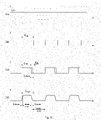
Fig. 2 and acting in the apparatus implementing the proposed method illustrate: - a) DC voltage U0 of the high
DC voltage source 1; - b) control square pulses with a preset duration, τsql, at the
first output 18 of thecontrol circuit 14; - c) control square pulses with a preset duration, τsqs,saw-tooth pulse voltage at the
output 35 of the converter33 of square pulse duration, τsqs = τsq1 - Δτ, where Δτ > τdiode is a value of a protective time interval securing pre-connecting the anode of thediode 22 to the negative terminal of the lowDC voltage source 12; - d) successive conditions of the diode 22: Diode is on, Diode is getting off during τdiode, and Diode is off;
- e) high pulse voltage between
terminals inductive load 2; - f) control pulses, of the τsq2 duration, at the
second output 53 of thecontrol circuit 14, these control pules being delayed relative the trailing edge of the square control pulses τsq1 at thefirst output 18 of thecontrol circuit 14 by the value of τsqd; - g) saw-tooth pulse voltage at the low-
ohmic resistor 11 of the first controlled gate 6 (which voltage reflects variations of current in the inductive load when the square control pulse with the preset duration τsq1 acts). - The apparatus for providing high pulse voltage in the inductive load, implementing the proposed method, operates as follows.
- Square pulses of the duration τsq1, (see Fig. 2b) come from the
output 18 of thecontrol circuit 14 to thecontrol input 19 of the first controlled gate 6 (to the gate of the MOS transistor) and thus open the first controlledgate 6. At that, the potential of thesecond terminal 8 of theinductive load 2 becomes close to zero relative to the potential of thenegative terminal 10 of the highDC voltage source 1 and the negative terminal 13 of the lowDC voltage source 12 connected to each other. Thus, the voltage difference between theterminals inductive load 2 becomes close to the value of the output voltage of the highDC voltage source 1, and theinductive load 2 starts building up a high voltage square pulse (relative to the positive terminal 5 of the high DC voltage source 1) which is transformed into the secondary winding of thetransformer 3. At the same time, square pulses from thefirst output 18 of thecontrol circuit 14 come to thecontrol input 34 of thefirst converter 33 of square pulse duration, which generates at theoutput 35 thereof a square pulse of the duration of τsqs = τsq1 - Δτ (see the flow chart of Fig. 2c) which comes to thecontrol input 36 of the second (additional) controlledswitch 28. - By the action of the above-discussed control pulse, the second controlled
switch 28 connects thefirst input 29 thereof (connected to thepositive terminal 16 of the low DC voltage source 12) to theoutput 30 thereof (connected to theanode 31 of the diode 22). Consequently, current starts flowing from thepositive terminal 16 of the lowDC voltage source 12 through the second controlledswitch 28, openeddiode 22,first capacitor 20 and opened first controlledgate 6. This current is charging thefirst capacitor 20, thus creating voltage on theplates DC voltage source 12. After the controlling pulse of the duration τsqs = τsq1 - Δτ ends at thecontrol input 36 of the second controlledswitch 28, theswitch 28 connects thesecond input 32 thereof (connected with the negative terminal 13 of the low DC voltage source 12) to theoutput 30 thereof (connected with the anode of the diode 22). - Accordingly, the
diode 22 turns off since applied to thecathode 23 thereof is the voltage between the plates of thefirst capacitor 20 charged earlier, the voltage being close to the output voltage of the lowDC voltage source 12. Because ofdiode 22 response time, the turning off thereof takes time of τdiode (seechart 2d inFig. 2 ). - If the duration τsqs of the control pulse at the
output 35 of the squarepulse duration converter 33 is such that τsq1 - τsqs = Δτ > τdiode, then thediode 22 will be reliably off by the time of the ending of the control pulse of duration τsq1 at theoutput 18 of the control circuit 14 (seecharts 2c, d inFig. 2 ). - After the square pulse of the duration τsq1 coming to the
control input 19 of the first controlled gate 6 (the gate of the MOS transistor) ends, the first controlledgate 6 turns off, and high voltage equal to the sum of the output voltage of the highDC voltage source 1 and voltage betweenterminals inductive load 2 appears at the first terminal of the first controlled gate (the drain of the MOS transistor) connected to theterminal 8 of theinductive load 2. - At that moment, the voltage difference between
terminals inductive load 2 changes the sign thereof (seechart 2e inFig. 2 ) indicating the end of generating high pulse voltage of the negative polarity in the inductive load. - Due to the fact that by this time the
diode 22 has been reliably off (seechart 2d inFig. 2 ), no pulse current surge happens through the incompletely closeddiode 22 in the apparatus for generating high pulse voltage implementing the proposed method - unlike apparatuses which implement prior art methods. - Seen on
chart 2g inFig. 2 can be the pulse voltage at the low-ohmic resistor 11 of the first controlled gate 5 which reflects a change of current in theinductive load 2 during the action of the control square pulse of the preset duration τsq1. It shows that no short-time power pulse noise, caused in the prior art apparatuses by a surge of a pulse current through the incompletely closeddiode 22, occurs at the end of generating high pulse voltage of the negative polarity in theinductive load 2, this resulting in better electromagnetic compatibility. - When the first controlled
gate 6 turns off (after the control square pulse of the duration τsq1 ends), voltage appears essentially instantaneously at the first terminal 7 (the drain of the MOS transistor) thereof from the positive terminal 5 of the highDC voltage source 1 via theinductive load 2. This voltage, equal to the sum of the output voltage of the highDC voltage source 1 and voltage betweenterminals inductive load 2, is applied to thefirst plate 21 of thefirst capacitor 20, which was charged earlier to the voltage equal to the output voltage of the lowDC voltage source 12. Consequently, the voltage difference between the first, 26, and second, 27, inputs of the first controlledswitch 25 remains approximately equal to the output voltage of the lowDC voltage source 12 but shifted (relative to the potential of thenegative terminal 10 of the highDC voltage source 1 and the negative terminal 13 of the lowDC voltage source 12 connected to each other) by the value equal to the sum of the output voltage of the highDC voltage source 1 and voltage betweenterminals inductive load 2. - From the
output 50 of thesquare pulse generator 47 of thecontrol circuit 14, square pulses, having passed through thedelay element 48 and the squarepulse duration converter 49 of thecontrol circuit 14 and having been converted as illustrated inchart 2f inFig. 2 , come to thecontrol input 54 of the first controlledswitch 25. - By the action of those pulses of the duration τsq2 , the first controlled
switch 25 connects thefirst input 27 thereof with theoutput 46 thereof, thus connecting, respectively, thesecond plate 24 of thefirst capacitor 20 with thecontrol input 45 of the second controlledgate 41. - As a result of that, the second controlled
gate 41 goes open since a potential at theoutput 46 of the first controlledswitch 25 turns out to be higher than the potential of the second terminal 44 (the source of the MOS transistor) of the second controlledgate 41 by the value of voltage between theplates gate 41 is on, recharging thesecond capacitor 39 takes place in the circuit including thefirst terminal 4 of theinductive load 2, thesecond capacitor 39, the open second controlledgate 41, and thesecond terminal 8 of theinductive load 2. - After the control square pulse of the duration τsq2 at the control input of the first controlled
switch 25 ends, the controlledgates charts Fig. 2 ), and dumped vibrations illustrated inchart 2e ofFig. 2 appear in a resonant circuit formed bytransformer 3 primary winding leakage inductance andtransformer 3 spurious capacitance (not shown). At the moment of minimal value of voltage at the first (main)terminal 7 of the first controlled gate 6 (drain of the MOS transistor), a control square pulse of the duration τsq1 from theoutput 18 of thecontrol circuit 14 is again applied to thecontrol input 19 of the first controlledgate 25, and the all the processes repeat themselves. - In this way, the proposed method of generating high pulse voltage in the inductive load allows providing apparatuses advantageously differing from the prior art in lesser level of noise radiated into the environment.
- Functional units composing the above-discussed apparatus can be implemented in various ways. The square
pulse duration converters switches
Claims (1)
- A method of generating high pulse voltage in an inductive load, the method comprising:- providing high DC voltage using a high DC voltage source (1) and providing low DC voltage using a low DC voltage source (12);- generating a first sequence of controlling square pulses having a preset duration of pulses (τsq1);- applying said first sequence to a control input (19) of a first controlled gate (6) for periodically connecting an inductive load (2) to outputs (5, 10) of said high DC voltage source (1) thus obtaining high pulse voltage having the preset duration of pulses (τsq1) in said inductive load (2); as well as- generating a second sequence of controlling square pulses having another preset duration of pulses (τsq2), these control pulses being delayed relative to the trailing edge of the control pulses of the first sequence by a value (τsqd);- applying said second sequence to a control input (54) of a first controlled switch (25) for periodically disconnecting and connecting a control input (45) of a second controlled gate (41) via said first controlled switch (25) to a first plate (21) of a capacitor (20) connected to a second terminal (8) of the inductive load (2) or to a second plate (24) of the capacitor (20) connected to a cathode (23) of a diode (22), wherein said control input (45) is connected to an output (46) of said first controlled switch (25); wherein a second capacitor (39) is connected by a first plate (40) thereof to a positive one of the outputs (5, 10) of the high DC voltage source (1) and to a first terminal (4) of the inductive load (2) and wherein the second controlled gate (41) is connected by a first terminal (42) thereof to a second plate (43) of the second capacitor (39) and is connected by a second terminal (44) thereof to the second terminal (8) of the inductive load (2);
characterized in that
in order to prevent short-term pulse electromagnetic noise from occurring- said first sequence of controlling pulses is transformed into a third sequence of controlling pulses, the result of the transformation being that trailing edges of the pulses of said third sequence are leading trailing edges of the pulses of said first sequence by a preset value, equal or greater than a response time of the diode (22); and- applying said third sequence of controlling pulses to a control input (36) of a second controlled switch (28), wherein said switch (28) is connected by an output (30) thereof to an anode (31) of the diode (22), said switch (28) periodically applying low voltage from an output (16) of said low DC voltage source (12) to the capacitor (20) via said diode (22).
Applications Claiming Priority (1)
| Application Number | Priority Date | Filing Date | Title |
|---|---|---|---|
| PCT/RU2016/000271 WO2017192058A1 (en) | 2016-05-04 | 2016-05-04 | Method for generating a high pulse voltage in an inductive load |
Publications (3)
| Publication Number | Publication Date |
|---|---|
| EP3454462A1 EP3454462A1 (en) | 2019-03-13 |
| EP3454462A4 EP3454462A4 (en) | 2019-11-27 |
| EP3454462B1 true EP3454462B1 (en) | 2022-06-22 |
Family
ID=60202958
Family Applications (1)
| Application Number | Title | Priority Date | Filing Date |
|---|---|---|---|
| EP16901111.1A Active EP3454462B1 (en) | 2016-05-04 | 2016-05-04 | Method for generating a high pulse voltage in an inductive load |
Country Status (6)
| Country | Link |
|---|---|
| US (1) | US10355599B2 (en) |
| EP (1) | EP3454462B1 (en) |
| JP (1) | JP6782306B2 (en) |
| CN (1) | CN109075694B (en) |
| RU (1) | RU2701553C1 (en) |
| WO (1) | WO2017192058A1 (en) |
Families Citing this family (2)
| Publication number | Priority date | Publication date | Assignee | Title |
|---|---|---|---|---|
| KR102054359B1 (en) * | 2017-01-10 | 2019-12-10 | 클로스드-업 조인트-스톡 컴파니 드라이브 | DC voltage-pulse voltage conversion method |
| WO2018199788A1 (en) * | 2017-04-24 | 2018-11-01 | Закрытое Акционерное Общество "Драйв" | Device for generating a high pulse voltage |
Family Cites Families (24)
| Publication number | Priority date | Publication date | Assignee | Title |
|---|---|---|---|---|
| SU864468A1 (en) * | 1978-06-05 | 1981-09-15 | Институт Электродинамики Ан Усср | Dc-to-ac voltage converter |
| US5173846A (en) * | 1991-03-13 | 1992-12-22 | Astec International Ltd. | Zero voltage switching power converter |
| US5687067A (en) * | 1995-05-30 | 1997-11-11 | Philips Electronics North America Corporation | Low noise controller for pulse width modulated converters |
| US5896279A (en) * | 1997-04-10 | 1999-04-20 | Api Technology Co., Ltd. | Constant-voltage clamping forward conversion switching power supply |
| US6069803A (en) * | 1999-02-12 | 2000-05-30 | Astec International Limited | Offset resonance zero volt switching flyback converter |
| JP2002027752A (en) * | 2000-07-07 | 2002-01-25 | Sony Corp | Switching power supply circuit |
| US6466462B2 (en) * | 2000-10-31 | 2002-10-15 | Yokogawa Electric Corporation | DC/DC converter having a control circuit to reduce losses at light loads |
| JP3707409B2 (en) * | 2001-09-10 | 2005-10-19 | 株式会社村田製作所 | Switching power supply |
| US7006364B2 (en) * | 2004-03-15 | 2006-02-28 | Delta Electronics, Inc. | Driving circuit for DC/DC converter |
| RU2264685C1 (en) * | 2004-04-01 | 2005-11-20 | Общество с ограниченной ответственностью Научно-производственное предприятие НПП "Поликоммуникационные системы" | Regulated voltage converter |
| US7286376B2 (en) * | 2005-11-23 | 2007-10-23 | System General Corp. | Soft-switching power converter having power saving circuit for light load operations |
| US8488348B2 (en) * | 2007-06-20 | 2013-07-16 | Samsung Electronics Co., Ltd. | Switch mode power supply apparatus having active clamping circuit |
| US7869235B2 (en) * | 2008-04-28 | 2011-01-11 | Fsp Technology Inc. | Flyback converter having an active snubber |
| JP4952807B2 (en) * | 2010-02-10 | 2012-06-13 | サンケン電気株式会社 | Active snubber circuit and power supply circuit |
| US20110305048A1 (en) * | 2010-06-11 | 2011-12-15 | System General Corp. | Active-clamp circuit for quasi-resonant flyback power converter |
| CN102891608B (en) * | 2011-07-21 | 2016-03-30 | 山特电子(深圳)有限公司 | A kind of high-efficiency and low-cost Forward-flyback DC-DC converter topology |
| JP6073077B2 (en) * | 2012-05-30 | 2017-02-01 | 株式会社テーケィアール | Switching power supply and electronic device equipped with switching power supply |
| RU2510764C2 (en) * | 2012-08-07 | 2014-04-10 | Закрытое Акционерное Общество "Драйв" | Device for generation of alternating current passing in load supply circuit |
| EP2951910B1 (en) * | 2013-01-30 | 2018-11-21 | Schneider Electric IT Corporation | Flyback converter |
| US9246392B2 (en) * | 2013-03-13 | 2016-01-26 | Power Integrations, Inc. | Switched mode power converter controller with ramp time modulation |
| US10038387B2 (en) * | 2013-04-15 | 2018-07-31 | Semiconductor Components Industries, Llc | Control circuit for active clamp flyback power converter with predicted timing control |
| RU2674010C2 (en) * | 2014-05-12 | 2018-12-04 | Закрытое Акционерное Общество "Драйв" | Device for producing direct current flowing in power supply circuit of load |
| US9991800B2 (en) * | 2015-05-20 | 2018-06-05 | Semiconductor Components Industries, Llc | Switched mode power supply with efficient operation at light loads and method therefor |
| US10050516B2 (en) * | 2016-03-29 | 2018-08-14 | Semiconductor Components Industries, Llc | Active clamp power converter and method of reducing shoot-through current during soft start |
-
2016
- 2016-05-04 EP EP16901111.1A patent/EP3454462B1/en active Active
- 2016-05-04 RU RU2018126218A patent/RU2701553C1/en active
- 2016-05-04 CN CN201680085051.6A patent/CN109075694B/en active Active
- 2016-05-04 JP JP2018555275A patent/JP6782306B2/en active Active
- 2016-05-04 WO PCT/RU2016/000271 patent/WO2017192058A1/en unknown
- 2016-05-04 US US16/092,693 patent/US10355599B2/en active Active
Also Published As
| Publication number | Publication date |
|---|---|
| WO2017192058A1 (en) | 2017-11-09 |
| EP3454462A1 (en) | 2019-03-13 |
| US20190165682A1 (en) | 2019-05-30 |
| RU2701553C1 (en) | 2019-09-30 |
| CN109075694B (en) | 2020-10-23 |
| CN109075694A (en) | 2018-12-21 |
| JP6782306B2 (en) | 2020-11-11 |
| JP2020509720A (en) | 2020-03-26 |
| EP3454462A4 (en) | 2019-11-27 |
| US10355599B2 (en) | 2019-07-16 |
Similar Documents
| Publication | Publication Date | Title |
|---|---|---|
| US10734906B2 (en) | Nanosecond pulser | |
| TWI424673B (en) | Synchronous rectifier control system and method for synchronous boost converter | |
| US10554128B2 (en) | Multi-level boost converter | |
| US6781853B2 (en) | Method and apparatus for reduction of energy loss due to body diode conduction in synchronous rectifiers | |
| EP0474471B1 (en) | Fixed frequency single ended forward converter switching at zero voltage | |
| EP2066012B1 (en) | Self-supply circuit and method for a voltage converter | |
| US6061255A (en) | Drive circuit for synchronous rectifiers in isolated forward converter | |
| CN103997213B (en) | The saturation of forward converter transformer is prevented | |
| US9787179B1 (en) | Apparatus and methods for control of discontinuous-mode power converters | |
| JP2014180199A (en) | Controller to be used in power converter, and power converter | |
| US6744647B2 (en) | Parallel connected converters apparatus and methods using switching cycle with energy holding state | |
| EP3454462B1 (en) | Method for generating a high pulse voltage in an inductive load | |
| TWI514730B (en) | Ultra high step-down converter | |
| JP6803993B2 (en) | DC voltage converter and how to operate the DC voltage converter | |
| US10361638B2 (en) | Apparatus for generating high pulse voltage | |
| JP2005507628A (en) | Synchronous rectifier circuit | |
| US6704211B1 (en) | DC-to-DC converter | |
| CN100438295C (en) | Multiple output DC-DC converter | |
| EP3618276B1 (en) | Device for generating a high pulse voltage | |
| Rao et al. | Design of buck type switched-mode power supplies using non-ideal components | |
| JP2005117884A (en) | Power supply | |
| JP2001119944A (en) | Direct current-to-direct current converter | |
| JPH05509220A (en) | Single-ended forward power converter with a transformer and two electronic switches protected by protective measures | |
| JPH0564445A (en) | Dc-dc converter | |
| JP2018046700A (en) | Insulation type switching power source device and power source control device |
Legal Events
| Date | Code | Title | Description |
|---|---|---|---|
| STAA | Information on the status of an ep patent application or granted ep patent |
Free format text: STATUS: THE INTERNATIONAL PUBLICATION HAS BEEN MADE |
|
| PUAI | Public reference made under article 153(3) epc to a published international application that has entered the european phase |
Free format text: ORIGINAL CODE: 0009012 |
|
| STAA | Information on the status of an ep patent application or granted ep patent |
Free format text: STATUS: REQUEST FOR EXAMINATION WAS MADE |
|
| 17P | Request for examination filed |
Effective date: 20181119 |
|
| AK | Designated contracting states |
Kind code of ref document: A1 Designated state(s): AL AT BE BG CH CY CZ DE DK EE ES FI FR GB GR HR HU IE IS IT LI LT LU LV MC MK MT NL NO PL PT RO RS SE SI SK SM TR |
|
| AX | Request for extension of the european patent |
Extension state: BA ME |
|
| DAV | Request for validation of the european patent (deleted) | ||
| DAX | Request for extension of the european patent (deleted) | ||
| A4 | Supplementary search report drawn up and despatched |
Effective date: 20191025 |
|
| RIC1 | Information provided on ipc code assigned before grant |
Ipc: H02M 1/12 20060101AFI20191021BHEP Ipc: H02M 1/14 20060101ALI20191021BHEP Ipc: H02M 1/34 20070101ALI20191021BHEP Ipc: H02M 3/335 20060101ALI20191021BHEP |
|
| STAA | Information on the status of an ep patent application or granted ep patent |
Free format text: STATUS: EXAMINATION IS IN PROGRESS |
|
| 17Q | First examination report despatched |
Effective date: 20201008 |
|
| STAA | Information on the status of an ep patent application or granted ep patent |
Free format text: STATUS: EXAMINATION IS IN PROGRESS |
|
| STAA | Information on the status of an ep patent application or granted ep patent |
Free format text: STATUS: EXAMINATION IS IN PROGRESS |
|
| REG | Reference to a national code |
Ref country code: DE Ref legal event code: R079 Ref document number: 602016073079 Country of ref document: DE Free format text: PREVIOUS MAIN CLASS: H02M0001120000 Ipc: H02M0001080000 |
|
| RIC1 | Information provided on ipc code assigned before grant |
Ipc: H02M 3/335 20060101ALI20220131BHEP Ipc: H02M 1/44 20070101ALI20220131BHEP Ipc: H02M 1/08 20060101AFI20220131BHEP |
|
| GRAP | Despatch of communication of intention to grant a patent |
Free format text: ORIGINAL CODE: EPIDOSNIGR1 |
|
| STAA | Information on the status of an ep patent application or granted ep patent |
Free format text: STATUS: GRANT OF PATENT IS INTENDED |
|
| INTG | Intention to grant announced |
Effective date: 20220316 |
|
| GRAS | Grant fee paid |
Free format text: ORIGINAL CODE: EPIDOSNIGR3 |
|
| GRAA | (expected) grant |
Free format text: ORIGINAL CODE: 0009210 |
|
| STAA | Information on the status of an ep patent application or granted ep patent |
Free format text: STATUS: THE PATENT HAS BEEN GRANTED |
|
| AK | Designated contracting states |
Kind code of ref document: B1 Designated state(s): AL AT BE BG CH CY CZ DE DK EE ES FI FR GB GR HR HU IE IS IT LI LT LU LV MC MK MT NL NO PL PT RO RS SE SI SK SM TR |
|
| REG | Reference to a national code |
Ref country code: GB Ref legal event code: FG4D |
|
| REG | Reference to a national code |
Ref country code: CH Ref legal event code: EP |
|
| REG | Reference to a national code |
Ref country code: DE Ref legal event code: R096 Ref document number: 602016073079 Country of ref document: DE |
|
| REG | Reference to a national code |
Ref country code: AT Ref legal event code: REF Ref document number: 1500429 Country of ref document: AT Kind code of ref document: T Effective date: 20220715 |
|
| REG | Reference to a national code |
Ref country code: IE Ref legal event code: FG4D |
|
| REG | Reference to a national code |
Ref country code: LT Ref legal event code: MG9D |
|
| REG | Reference to a national code |
Ref country code: NL Ref legal event code: MP Effective date: 20220622 |
|
| PG25 | Lapsed in a contracting state [announced via postgrant information from national office to epo] |
Ref country code: SE Free format text: LAPSE BECAUSE OF FAILURE TO SUBMIT A TRANSLATION OF THE DESCRIPTION OR TO PAY THE FEE WITHIN THE PRESCRIBED TIME-LIMIT Effective date: 20220622 Ref country code: NO Free format text: LAPSE BECAUSE OF FAILURE TO SUBMIT A TRANSLATION OF THE DESCRIPTION OR TO PAY THE FEE WITHIN THE PRESCRIBED TIME-LIMIT Effective date: 20220922 Ref country code: LT Free format text: LAPSE BECAUSE OF FAILURE TO SUBMIT A TRANSLATION OF THE DESCRIPTION OR TO PAY THE FEE WITHIN THE PRESCRIBED TIME-LIMIT Effective date: 20220622 Ref country code: HR Free format text: LAPSE BECAUSE OF FAILURE TO SUBMIT A TRANSLATION OF THE DESCRIPTION OR TO PAY THE FEE WITHIN THE PRESCRIBED TIME-LIMIT Effective date: 20220622 Ref country code: GR Free format text: LAPSE BECAUSE OF FAILURE TO SUBMIT A TRANSLATION OF THE DESCRIPTION OR TO PAY THE FEE WITHIN THE PRESCRIBED TIME-LIMIT Effective date: 20220923 Ref country code: FI Free format text: LAPSE BECAUSE OF FAILURE TO SUBMIT A TRANSLATION OF THE DESCRIPTION OR TO PAY THE FEE WITHIN THE PRESCRIBED TIME-LIMIT Effective date: 20220622 Ref country code: BG Free format text: LAPSE BECAUSE OF FAILURE TO SUBMIT A TRANSLATION OF THE DESCRIPTION OR TO PAY THE FEE WITHIN THE PRESCRIBED TIME-LIMIT Effective date: 20220922 |
|
| REG | Reference to a national code |
Ref country code: AT Ref legal event code: MK05 Ref document number: 1500429 Country of ref document: AT Kind code of ref document: T Effective date: 20220622 |
|
| PG25 | Lapsed in a contracting state [announced via postgrant information from national office to epo] |
Ref country code: RS Free format text: LAPSE BECAUSE OF FAILURE TO SUBMIT A TRANSLATION OF THE DESCRIPTION OR TO PAY THE FEE WITHIN THE PRESCRIBED TIME-LIMIT Effective date: 20220622 Ref country code: LV Free format text: LAPSE BECAUSE OF FAILURE TO SUBMIT A TRANSLATION OF THE DESCRIPTION OR TO PAY THE FEE WITHIN THE PRESCRIBED TIME-LIMIT Effective date: 20220622 |
|
| PG25 | Lapsed in a contracting state [announced via postgrant information from national office to epo] |
Ref country code: NL Free format text: LAPSE BECAUSE OF FAILURE TO SUBMIT A TRANSLATION OF THE DESCRIPTION OR TO PAY THE FEE WITHIN THE PRESCRIBED TIME-LIMIT Effective date: 20220622 |
|
| PG25 | Lapsed in a contracting state [announced via postgrant information from national office to epo] |
Ref country code: SM Free format text: LAPSE BECAUSE OF FAILURE TO SUBMIT A TRANSLATION OF THE DESCRIPTION OR TO PAY THE FEE WITHIN THE PRESCRIBED TIME-LIMIT Effective date: 20220622 Ref country code: SK Free format text: LAPSE BECAUSE OF FAILURE TO SUBMIT A TRANSLATION OF THE DESCRIPTION OR TO PAY THE FEE WITHIN THE PRESCRIBED TIME-LIMIT Effective date: 20220622 Ref country code: RO Free format text: LAPSE BECAUSE OF FAILURE TO SUBMIT A TRANSLATION OF THE DESCRIPTION OR TO PAY THE FEE WITHIN THE PRESCRIBED TIME-LIMIT Effective date: 20220622 Ref country code: PT Free format text: LAPSE BECAUSE OF FAILURE TO SUBMIT A TRANSLATION OF THE DESCRIPTION OR TO PAY THE FEE WITHIN THE PRESCRIBED TIME-LIMIT Effective date: 20221024 Ref country code: ES Free format text: LAPSE BECAUSE OF FAILURE TO SUBMIT A TRANSLATION OF THE DESCRIPTION OR TO PAY THE FEE WITHIN THE PRESCRIBED TIME-LIMIT Effective date: 20220622 Ref country code: EE Free format text: LAPSE BECAUSE OF FAILURE TO SUBMIT A TRANSLATION OF THE DESCRIPTION OR TO PAY THE FEE WITHIN THE PRESCRIBED TIME-LIMIT Effective date: 20220622 Ref country code: CZ Free format text: LAPSE BECAUSE OF FAILURE TO SUBMIT A TRANSLATION OF THE DESCRIPTION OR TO PAY THE FEE WITHIN THE PRESCRIBED TIME-LIMIT Effective date: 20220622 Ref country code: AT Free format text: LAPSE BECAUSE OF FAILURE TO SUBMIT A TRANSLATION OF THE DESCRIPTION OR TO PAY THE FEE WITHIN THE PRESCRIBED TIME-LIMIT Effective date: 20220622 |
|
| PG25 | Lapsed in a contracting state [announced via postgrant information from national office to epo] |
Ref country code: PL Free format text: LAPSE BECAUSE OF FAILURE TO SUBMIT A TRANSLATION OF THE DESCRIPTION OR TO PAY THE FEE WITHIN THE PRESCRIBED TIME-LIMIT Effective date: 20220622 Ref country code: IS Free format text: LAPSE BECAUSE OF FAILURE TO SUBMIT A TRANSLATION OF THE DESCRIPTION OR TO PAY THE FEE WITHIN THE PRESCRIBED TIME-LIMIT Effective date: 20221022 |
|
| REG | Reference to a national code |
Ref country code: DE Ref legal event code: R097 Ref document number: 602016073079 Country of ref document: DE |
|
| PG25 | Lapsed in a contracting state [announced via postgrant information from national office to epo] |
Ref country code: AL Free format text: LAPSE BECAUSE OF FAILURE TO SUBMIT A TRANSLATION OF THE DESCRIPTION OR TO PAY THE FEE WITHIN THE PRESCRIBED TIME-LIMIT Effective date: 20220622 |
|
| PG25 | Lapsed in a contracting state [announced via postgrant information from national office to epo] |
Ref country code: DK Free format text: LAPSE BECAUSE OF FAILURE TO SUBMIT A TRANSLATION OF THE DESCRIPTION OR TO PAY THE FEE WITHIN THE PRESCRIBED TIME-LIMIT Effective date: 20220622 |
|
| PLBE | No opposition filed within time limit |
Free format text: ORIGINAL CODE: 0009261 |
|
| STAA | Information on the status of an ep patent application or granted ep patent |
Free format text: STATUS: NO OPPOSITION FILED WITHIN TIME LIMIT |
|
| 26N | No opposition filed |
Effective date: 20230323 |
|
| PG25 | Lapsed in a contracting state [announced via postgrant information from national office to epo] |
Ref country code: SI Free format text: LAPSE BECAUSE OF FAILURE TO SUBMIT A TRANSLATION OF THE DESCRIPTION OR TO PAY THE FEE WITHIN THE PRESCRIBED TIME-LIMIT Effective date: 20220622 |
|
| PG25 | Lapsed in a contracting state [announced via postgrant information from national office to epo] |
Ref country code: MC Free format text: LAPSE BECAUSE OF FAILURE TO SUBMIT A TRANSLATION OF THE DESCRIPTION OR TO PAY THE FEE WITHIN THE PRESCRIBED TIME-LIMIT Effective date: 20220622 |
|
| REG | Reference to a national code |
Ref country code: BE Ref legal event code: MM Effective date: 20230531 |
|
| PG25 | Lapsed in a contracting state [announced via postgrant information from national office to epo] |
Ref country code: MC Free format text: LAPSE BECAUSE OF FAILURE TO SUBMIT A TRANSLATION OF THE DESCRIPTION OR TO PAY THE FEE WITHIN THE PRESCRIBED TIME-LIMIT Effective date: 20220622 Ref country code: LU Free format text: LAPSE BECAUSE OF NON-PAYMENT OF DUE FEES Effective date: 20230504 Ref country code: IT Free format text: LAPSE BECAUSE OF FAILURE TO SUBMIT A TRANSLATION OF THE DESCRIPTION OR TO PAY THE FEE WITHIN THE PRESCRIBED TIME-LIMIT Effective date: 20220622 |
|
| REG | Reference to a national code |
Ref country code: IE Ref legal event code: MM4A |
|
| PG25 | Lapsed in a contracting state [announced via postgrant information from national office to epo] |
Ref country code: IE Free format text: LAPSE BECAUSE OF NON-PAYMENT OF DUE FEES Effective date: 20230504 |
|
| PG25 | Lapsed in a contracting state [announced via postgrant information from national office to epo] |
Ref country code: IE Free format text: LAPSE BECAUSE OF NON-PAYMENT OF DUE FEES Effective date: 20230504 |
|
| PG25 | Lapsed in a contracting state [announced via postgrant information from national office to epo] |
Ref country code: BE Free format text: LAPSE BECAUSE OF NON-PAYMENT OF DUE FEES Effective date: 20230531 |
|
| PGFP | Annual fee paid to national office [announced via postgrant information from national office to epo] |
Ref country code: GB Payment date: 20240521 Year of fee payment: 9 |
|
| PGFP | Annual fee paid to national office [announced via postgrant information from national office to epo] |
Ref country code: DE Payment date: 20240311 Year of fee payment: 9 |
|
| PGFP | Annual fee paid to national office [announced via postgrant information from national office to epo] |
Ref country code: CH Payment date: 20240602 Year of fee payment: 9 |
|
| PGFP | Annual fee paid to national office [announced via postgrant information from national office to epo] |
Ref country code: FR Payment date: 20240528 Year of fee payment: 9 |
|
| PG25 | Lapsed in a contracting state [announced via postgrant information from national office to epo] |
Ref country code: BG Free format text: LAPSE BECAUSE OF FAILURE TO SUBMIT A TRANSLATION OF THE DESCRIPTION OR TO PAY THE FEE WITHIN THE PRESCRIBED TIME-LIMIT Effective date: 20220622 |
|
| PG25 | Lapsed in a contracting state [announced via postgrant information from national office to epo] |
Ref country code: BG Free format text: LAPSE BECAUSE OF FAILURE TO SUBMIT A TRANSLATION OF THE DESCRIPTION OR TO PAY THE FEE WITHIN THE PRESCRIBED TIME-LIMIT Effective date: 20220622 |