EP3364476B1 - Active oled display, method for preparing an active oled display and compound - Google Patents
Active oled display, method for preparing an active oled display and compound Download PDFInfo
- Publication number
- EP3364476B1 EP3364476B1 EP17156902.3A EP17156902A EP3364476B1 EP 3364476 B1 EP3364476 B1 EP 3364476B1 EP 17156902 A EP17156902 A EP 17156902A EP 3364476 B1 EP3364476 B1 EP 3364476B1
- Authority
- EP
- European Patent Office
- Prior art keywords
- hole transport
- dopant
- iii
- display device
- mol
- Prior art date
- Legal status (The legal status is an assumption and is not a legal conclusion. Google has not performed a legal analysis and makes no representation as to the accuracy of the status listed.)
- Active
Links
Images

Classifications
-
- H—ELECTRICITY
- H10—SEMICONDUCTOR DEVICES; ELECTRIC SOLID-STATE DEVICES NOT OTHERWISE PROVIDED FOR
- H10K—ORGANIC ELECTRIC SOLID-STATE DEVICES
- H10K59/00—Integrated devices, or assemblies of multiple devices, comprising at least one organic light-emitting element covered by group H10K50/00
- H10K59/30—Devices specially adapted for multicolour light emission
- H10K59/35—Devices specially adapted for multicolour light emission comprising red-green-blue [RGB] subpixels
-
- H—ELECTRICITY
- H10—SEMICONDUCTOR DEVICES; ELECTRIC SOLID-STATE DEVICES NOT OTHERWISE PROVIDED FOR
- H10K—ORGANIC ELECTRIC SOLID-STATE DEVICES
- H10K50/00—Organic light-emitting devices
- H10K50/10—OLEDs or polymer light-emitting diodes [PLED]
- H10K50/14—Carrier transporting layers
- H10K50/15—Hole transporting layers
- H10K50/155—Hole transporting layers comprising dopants
-
- H—ELECTRICITY
- H10—SEMICONDUCTOR DEVICES; ELECTRIC SOLID-STATE DEVICES NOT OTHERWISE PROVIDED FOR
- H10K—ORGANIC ELECTRIC SOLID-STATE DEVICES
- H10K85/00—Organic materials used in the body or electrodes of devices covered by this subclass
- H10K85/30—Coordination compounds
- H10K85/321—Metal complexes comprising a group IIIA element, e.g. Tris (8-hydroxyquinoline) gallium [Gaq3]
- H10K85/322—Metal complexes comprising a group IIIA element, e.g. Tris (8-hydroxyquinoline) gallium [Gaq3] comprising boron
-
- H—ELECTRICITY
- H10—SEMICONDUCTOR DEVICES; ELECTRIC SOLID-STATE DEVICES NOT OTHERWISE PROVIDED FOR
- H10K—ORGANIC ELECTRIC SOLID-STATE DEVICES
- H10K85/00—Organic materials used in the body or electrodes of devices covered by this subclass
- H10K85/30—Coordination compounds
- H10K85/381—Metal complexes comprising a group IIB metal element, e.g. comprising cadmium, mercury or zinc
Definitions
- the disclosure relates to an active OLED display having a plurality of OLED pixels and comprising a non-oxidizing p-dopant in a hole injection and/or hole transport layer shared by at least two pixels, a method of preparing the active OLED display and to a compound particularly suitable for the display.
- JP2010/087276 A discloses an OLED display comprising a common hole transporting layer shared by a plurality of pixels and containing a metal salt or an organic salt. There is, however, continuing demand for p-dopants fulfilling these criteria and improved in other parameters, e.g. from the viewpoint of processability and device stability.
- the improved materials should enable robust display manufacturing, e.g. in terms of improved device stability during any processing step which comprises a treatment of the device or its particular layer at an elevated temperature.
- the object is achieved through a display device comprising
- the anion and/or the anionic ligand is bound to the metal cation of the p-dopant through an oxygen atom, preferably through two oxygen atoms.
- bound encompasses structures of the p-dopant, wherein the distance between the metal cation and the oxygen atom/atoms is shorter that the distance between the metal cation and any other atom of the anion and/or of the anionic ligand.
- the oxygen atom of the anion and/or of the anionic ligand which is in the metal salt and/or in the metal complex bound to the metal cation has in dichloroethane lower basicity than at least one non-oxygen atoms of the anion and/or of the anionic ligand.
- each of the oxygen atoms of the anion and/or of the anionic ligand which are in the metal salt and/or in the metal complex bound to the metal cation has in dichloroethane lower basicity than at least one non-oxygen atom of the anion and/or of the anionic ligand.
- the basicity of an atom in the anion and/or in the anionic ligand in an environment e.g. in 1,2-dichloroethane, is inversely proportional to the acidity of a corresponding tautomeric form of the electrically neutral conjugated acid formed by addition of one or more protons in the same environment.
- the anion and/or the anionic ligand consists of at least 6, more preferably at least 7, even more preferably at least 8, most preferably at least 9 covalently bound atoms.
- the anion and/or the anionic ligand comprises at least two atoms selected from B, C and N which are bound to each other by a covalent bond.
- the anion and/or the anionic ligand comprises at least one peripheral atom selected from H, N, O, F, Cl, Br and I.
- peripheral atom it is to be understood an atom which is covalently bound to only one atom of the anion and/or of the anionic ligand.
- atoms covalently bound to at least two other atoms of the anion and/or of the anionic ligand are assigned as inner atoms.
- the anion and/or the anionic ligand comprises at least one electron withdrawing group selected from halogenated alkyl, halogenated (hetero)aryl, halogenated (hetero)arylalkyl, halogenated alkylsulfonyl, halogenated (hetero)arylsulfonyl, halogenated (hetero)arylalkylsulfonyl, cyano.
- halogenated (hetero)aryl means “halogenated aryl or halogenated heteroaryl
- halogenated (hetero)arylalkyl means “halogenated heteroarylalkyl or halogenated arylalkyl
- halogenated (hetero)arylsulfonyl means "halogenated heteroarylsulfonyl or halogenated arylsulfonyl”
- halogenated (hetero)arylalkylsulfonyl means "halogenated heteroarylalkylsulfonyl or halogenated arylalkylsulfonyl”.
- the electron withdrawing group is a perhalogenated group.
- halogenated means that at least one hydrogen atom of a group comprising peripheral or inner hydrogen atoms is replaced with an atom selected from F, Cl, Br and I. It is further understood that in a perhalogenated group, all hydrogen atoms comprised in the unsubstituted group are replaced with atoms independently selected from F, Cl, Br and I. Accordingly, under perfluorinated group, it is to be understood a perhalogenated group, wherein all halogen atoms replacing hydrogen atoms are fluorine atoms.
- the metal cation of the p-dopant is selected from Li(I), Na(I), K(I), Rb(I), Cs(I); Mg(II), Ca(II), Sr(II), Ba(II), Sn(II), Pb(II), Mn(II), Fe(II), Co(II), Ni(II), Zn(II), Cd(II), Al(III); rare earth metal in oxidation state (III), V(III), Nb(III), Ta(III), Cr(III), Mo(III), W(III) Ga(III), In(III) and from Ti(IV), Zr(IV), Hf(IV), Sn(IV).
- the atom of the anion and/or of the anionic ligand which is closest to the metal cation is a C or a N atom.
- the acidity of the electrically neutral conjugated acid formed from the anion and/or anionic ligand by addition of one or more protons in 1,2-dichloroethane is higher than that of HCl, preferably higher than that of HBr, more preferably higher than that of HI, even more preferably higher than that of fluorosulfuric acid, and most preferably higher than that of perchloric acid.
- the electrical p-dopant has energy level of its highest unoccupied molecular orbital computed by standard quantum chemical method and expressed in absolute vacuum scale at least 0.5 eV, preferably at least 0.6 eV, more preferably at least 0.8 eV, even more preferably at least 1.0 eV, most preferably at least 1.2 eV above the energy level of the highest occupied orbital of the covalent hole transport compound computed by the standard quantum chemical method.
- the standard quantum chemical method may be the software package TURBOMOLE using DFT functional B3LYP with the basis set def2-TZVP.
- the first hole transport matrix compound is an organic compound, preferably an organic compound comprising a conjugated system of at least 6, more preferably at least 10 delocalized electrons; also preferably, the first hole transport matrix compound comprises at least one triaryl amine structural moiety, more preferably, the first hole transport matrix compound comprises at least two triaryl amine structural moieties.
- the object is further achieved by method for preparing the display device according to any of the preceding embodiments, the method comprising at least one step wherein the hole transport matrix compound and the electrical p-dopant are in mutual contact exposed to a temperature above 50 °C.
- the method may comprise the steps, wherein
- the method may further comprise at least one step wherein the p-dopant is evaporated at a reduced pressure, preferably at a pressure below 1 ⁇ 10 -2 Pa and at a temperature above 50 °C, more preferably at a pressure below 5 ⁇ 10 -2 Pa and at a temperature above 80 °C, even more preferably at a pressure below 1 ⁇ 10 -3 Pa and at a temperature above 120 °C, most preferably at a pressure below 5 ⁇ 10 -4 Pa and at a temperature above 150 °C.
- a reduced pressure preferably at a pressure below 1 ⁇ 10 -2 Pa and at a temperature above 50 °C, more preferably at a pressure below 5 ⁇ 10 -2 Pa and at a temperature above 80 °C, even more preferably at a pressure below 1 ⁇ 10 -3 Pa and at a temperature above 120 °C, most preferably at a pressure below 5 ⁇ 10 -4 Pa and at a temperature above 150 °C.
- the p-dopant may be used in form of a solid hydrate.
- the p-dopant may be used as an anhydrous solid comprising less than 0.10 wt% water, preferably less than 0.05 wt% water.
- M is selected from Mg(II), Mn(II) and Zn(II).
- the compound according to formula (I) is provided in a solid form, preferably in a solid form comprising less than 0.10 wt % water, more preferably in a solid form comprising less than 0.05 wt % water, most preferably in a solid crystalline form comprising less than 0.05 wt % water.
- the compound according to formula (I) is provided in form of a solid crystalline hydrate, preferably in form of a solid crystalline hydrate which has water content in the range
- An important property of materials comprised in organic semi-conducting devices is their conductivity.
- a limited conductivity of the shared layer may be favourable for achieving a low level of the undesired electrical crosstalk in the display.
- very low conductivity of the shared layer may increase the operational voltage of the display.
- WO2016/050834 teaches a conductivity range which represents a trade-off between these contradictory requirements.
- semiconducting materials and/or layers doped with these compounds exhibit well-measurable electrical conductivities which are only slightly lower in comparison with materials and/or layers doped with typical redox p-dopants. It appears that this mode occurs if the doped material and/or layer is exposed to oxygen, even though only in trace amounts.
- the semiconducting materials and/or layers doped with the disclosed metal salts and/or electrically neutral metal complexes comprising an anionic ligand exhibit hardly measurable electrical conductivities.
- This mode occurs if the oxygen access to the doped material and/or layer is strictly avoided throughout processing thereof.
- the authors found that despite the extremely low conductivity of materials and/or layers doped in the second mode, devices comprising such materials and/or layers particularly as hole transporting or hole injecting layers still exhibit electrical behavior corresponding to an excellent hole injection.
- the existence of the two above described modes of p-doping activity provides the disclosed p-dopants with a unique versatility in their use in organic electronic devices, and particularly in displays comprising an anode structured into a multiplicity of pixels sharing a common hole transport layer.
- the conductivity of the common p-doped layer can be either set in the limits taught in WO2016/050834 by exploiting the first doping mode, or set below these limits, exploiting the second doping mode.
- the materials and/or layers doped with the presented metal salts and/or metal complexes may exhibit favourable thermal stability, particularly in materials provided according to the above described second mode of the p-doping action.
- These properties may be again particularly suitable for the use of the disclosed p-dopants in AMOLED displays, because the necessity of structuring such displays into separate pixels often requires a thermal treatment of p-doped layers or using another treatment which may result in an unavoidable heating of a previously deposited p-doped layer.
- the authors provided new amide compounds comprising bulkier fluorinated side chains in comparison with the compounds tested in EP15181385 .
- This change resulted in favourable storage properties of the new compounds, which are substantially non-hygroscopic and remain solid even at high air humidity, whereas LiTFSI and analogous TFSI salts have tendency to deliquesce.
- the electrical conductivity of a thin layer sample can be measured by, for example, the so called two-point method. At this, a voltage is applied to the thin layer and the current flowing through the layer is measured. The resistance, respectively the electrical conductivity, results by considering the geometry of the contacts and the thickness of the layer of the sample.
- the experimental setup for conductivity measurement used by the authors of the present application enables deposition of p-doped layers as well as conductivity measurement under controlled conditions, especially with regard to contact of deposited layers with an atmosphere comprising oxygen.
- the whole deposition-measurement sequence may be carried out either in a glove-box or in a chamber comprising a controlled atmosphere, using solution processing techniques, or completely in a vacuum chamber, using vacuum thermal evaporation (VTE) as the method of choice, especially suitable for materials and/or layers doped in the second mode.
- VTE vacuum thermal evaporation
- the electrical conductivity of the first hole transport layer may be lower than 1 ⁇ 10 -6 S ⁇ m -1 , preferably lower than 1 ⁇ 10 -7 S ⁇ m -1 , more preferably lower than 1 ⁇ 10 -8 S ⁇ m -1 .
- the detection limit of the used conductivity measurement method is lower than 1 ⁇ 10 -6 S ⁇ m -1 , it is preferred that the conductivity of the first hole transport layer is lower than the detection limit.
- the first hole transport layer is formed for the plurality of OLED pixels in the OLED display.
- the first HTL extends over all pixels of the plurality of pixels in the OLED display.
- the cathode may be formed as a common cathode for the plurality of pixels.
- the common cathode may extend over all pixels of the plurality of pixels in the OLED display. Every individual pixel may have its own anode that may not touch anodes of other individual pixels.
- organic layers may be provided: a hole blocking layer, an electron injection layer, and/or an electron blocking layer.
- the active OLED display has driving circuit configured to separately drive the individual pixels of the plurality of pixels provided in the OLED display.
- a step of separately driving may comprise separate control of the driving current applied the individual pixels.
- the first HTL is made of a hole transport matrix (HTM) material electrically doped with the p-dopant.
- the hole transport matrix material may be electrically doped with more than one p-dopant.
- HTM material may consist of one or more HTM compounds, whereas the term hole transport material is a broader term used throughout this application for all semiconducting materials comprising at least one hole transport matrix compound.
- the hole transport matrix material is not particularly limited. Generally, it is any material consisting of covalently bound atoms which allows embedding the p-dopant.
- the hole transport matrix material may consist of one or more organic compounds.
- the first hole transport layer may have a thickness of less than 50 nm, less than 40 nm, less than 30 nm, less than 20 nm, or less than 15 nm.
- the first hole transport layer may have a thickness of more than 3 nm, more than 5 nm, more than 8 nm, or more than 10 nm.
- the anode may be made of a transparent conductive oxide (TCO), like indium tin oxide (ITO) or aluminium zinc oxide (AZO).
- TCO transparent conductive oxide
- ITO indium tin oxide
- AZO aluminium zinc oxide
- the anode may be made of one or more thin metallic layers leading to a semitransparent anode.
- the anode may be made of a thick metallic layer which is not transparent to visible light.
- the OLED pixel(s) may comprise an electron blocking layer (EBL) provided between the first hole transport layer and the light emitting layer.
- the EBL may be in direct contact with the first HTL and the EML.
- the electron blocking layer may be an electrically undoped layer (in other words, it may be free of an electrical dopant) made of an organic hole transport matrix material.
- the composition of the organic hole transport matrix material of the first hole transport layer may be the same as the composition of the organic hole transport matrix material of the electron blocking layer. In another embodiment of the invention, the composition of both hole transport matrix materials may be different.
- the EBL may have a layer thickness of more than 30 nm, more than 50 nm, more than 70 nm, more than 100 nm, or more than 110 nm.
- the thickness of the EBL may be less than 200 nm, less than 170 nm, less than 140 nm, or less than 130 nm.
- the common HTL may be thinner by about one order of magnitude.
- Each compound forming the electron blocking layer may have a highest occupied molecular orbital (HOMO) energy level, expressed in the absolute scale referring to vacuum energy level being zero, higher than a HOMO level of any compound forming the hole transport matrix material of the common hole transport layer.
- HOMO occupied molecular orbital
- the organic matrix material of the electron blocking layer may have a hole mobility which is equal to or higher than the hole mobility of the matrix material of the hole transport layer.
- the hole transport matrix (HTM) material of the common HTL and/or of the EBL may be selected from compounds comprising a conjugated system of delocalized electrons, the conjugated system comprising lone electron pairs of at least two tertiary amine nitrogen atoms.
- Suitable compounds for the hole transport matrix material of the doped hole transport layer and / or the common hole transport layer may be selected from the known hole transport matrices (HTMs), e.g. from triaryl amine compounds.
- HTMs for the doped hole transport material may be compounds comprising a conjugated system of delocalized electrons, wherein the conjugated system comprises lone electron pairs of at least two tertiary amine nitrogen atoms.
- Examples are N4,N4'-di(naphthalen-1-yl)-N4,N4'-diphenyl-[1,1'-biphenyl]-4,4'-diamine (HT1), and N4,N4, N4",N4"-tetra([1,1'-biphenyl]-4-yl)-[1,1':4',1"-terphenyl]-4,4"-diamine (HT4).
- terphenyldiamine HTMs is described e.g. in WO 2011/134458 A1 , US 2012/223296 A1 or WO 2013/135237 A1 ; 1,3-phenylenediamine matrices are described e.g. in WO 2014/060526 A1 .
- Many triaryl amine HTMs are commercially available.
- the light emitting layer of the OLED display may comprise a plurality of sub-regions, each of the sub-regions being assigned to one of the pixels from the plurality of pixels.
- the organic layer comprising EMLs of individual pixels may be patterned by known methods, for example, by fine-metal masking (FMM), laser induced thermal imaging (LITI), and / or ink-jet printing (IJP) in either top emission, bottom emission or bottom emission micro cavity (see, for example, Chung et al.
- FMM fine-metal masking
- LITI laser induced thermal imaging
- IJP ink-jet printing
- a common electron transport layer may be formed by the electron transport layers provided in the stack of organic layers of the plurality of OLED pixels.
- the common electron transport layer may comprise an organic electron transport matrix (ETM) material. Further, the common electron transport layer may comprise one or more n-dopants-.Suitable compounds for the ETM contain aromatic or heteroaromatic structural moieties, as disclosed e.g. in documents EP 1970 371 A1 or WO 2013/079217 A1 .
- ETM organic electron transport matrix
- the cathode can be made of a metal or a metal alloy with a low work function.
- Transparent cathodes made of a TCO are also well-known in the art.
- the stack of organic layers may be made of organic compounds having a molecular weight of less than 2000 g/mol.
- the organic compounds may have a molecular weight of less than 1000 g/mol.
- Fig. 1 a schematic representation of an active OLED display, the display having a plurality of OLED pixels
- Fig. 1 shows a schematic representation of an active OLED display 1 having a plurality of OLED pixels 2, 3, 4 provided in an OLED display 1.
- each pixel 2, 3, 4 is provided with an anode 2a, 3a, 4a being connected to a driving circuit (not shown).
- a driving circuit not shown.
- the anodes 2a, 3a, 4a are made of a TCO, for example of ITO.
- a cathode 6 is provided on top of an organic stack comprising an electrically doped hole transport layer (HTL) 7, an electron blocking layer (EBL) 5, a light emitting layer (EML) having sub-regions 2b, 3b, 4b assigned to the pixels 2, 3, 4 and being provided separately in an electron transport layer (ETL) 9.
- the sub-regions 2b, 3b, 4b can provide an RGB combination for a color display (R - red, G - green, B - blue).
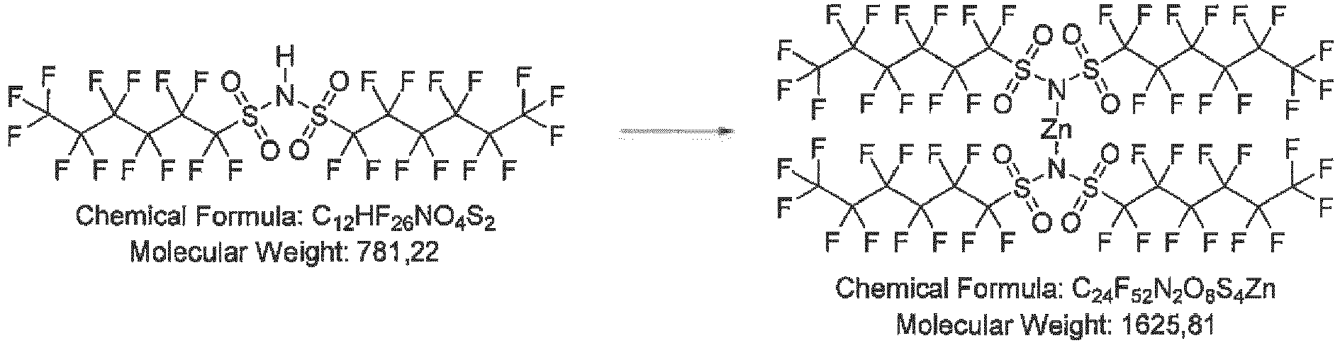
- Step 1 lithium bis((perfluorohexyl)sulfonyl)amide
- Step 2 lithium bis((perfluorohexyl)sulfonyl)amine
- Step 3 lithium bis((perfluorohexyl)sulfonyl)amide
- Mass spectroscopy with electrospray ionization confirmed the expected synthesis outcome by the dominant presence of m/z 780 (anion C 12 F 26 NO 4 S 2 ) in the intermediate bis((perfluorohexyl)sulfonyl)amine as well as in the Li salt.
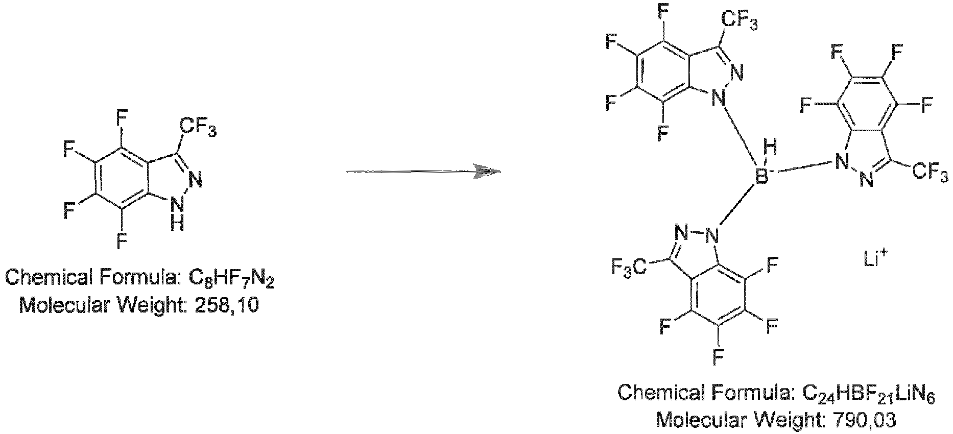
- Step 2 lithium tris(4,5,6,7-tetrafluoro-3-(trifluoromethyl)-1H-indazol-1-yl)hydroborate
- Step 1 4,5,6,7-tetrafluoro-3-(perfluorophenyl)-1H-indazole
- Step 2 lithium tris(4,5,6,7-tetrafluoro-3-(perfluorophenyl)-1H-indazol-1-yl)hydroborate
- the pressure tube is closed and heated to a temperature about 160 °C for ca 21 h. After cooling to room temperature, the mixture is treated with 5 mL hexane in an ultra-sonic bath for ca 30 min. The precipitated solid is filtered off and washed with hexane (20 mL in total). After drying, 0.48 g yellowish solid is obtained.
- Example 1 tandem OLED, model for bottom emitting white OLED pixel
- VTE vacuum thermal evaporation
- the operational voltage of the device 8 V was well comparable with the same device comprising a commercial state-of-art p-dopant instead of PB-1. Exact calibration of measuring equipment necessary for luminance/efficiency comparison was not made in this experiment..
- Example 2 bottom emitting blue OLED pixel
- VTE 10 nm hole injection layer made of the compound PB-1; 120 nm thick HTL made of neat F1; 20 nm EML made of ABH113 doped with 3 wt% NUBD370 (both supplied by SFC, Korea), 36 nm EIL/ETL made of F2 doped with 50 wt% LiQ; 100 nm Al cathode.
- Comparative device comprised the HIL made of the compound CN-HAT ( CAS 105598-27-4 ) instead of PB-1.
- the inventive device achieved current density 15 mA/cm 2 and external quantum efficiency (EQE) 5.4 % at an operational voltage 5.2 V, whereas the comparative device exhibited the same current density at a significantly higher voltage 5.4 V and with a significantly lower EQE 4.9 %.
Landscapes
- Chemical & Material Sciences (AREA)
- Inorganic Chemistry (AREA)
- Engineering & Computer Science (AREA)
- Materials Engineering (AREA)
- Physics & Mathematics (AREA)
- Optics & Photonics (AREA)
- Electroluminescent Light Sources (AREA)
Description
- The disclosure relates to an active OLED display having a plurality of OLED pixels and comprising a non-oxidizing p-dopant in a hole injection and/or hole transport layer shared by at least two pixels, a method of preparing the active OLED display and to a compound particularly suitable for the display.
- With respect to active OLED displays, comprising a plurality of OLED pixels sharing a common hole transport layer, challenging requirements are put on semiconducting materials used in layers arranged between the anode and the emitting layer and shared by the plurality of pixels. On one hand, the materials shall enable individual driving of individual pixels at operational voltages which are as low as possible. On the other hand, so called electrical crosstalk between neighbour pixels should be avoided. The application
WO2016/050834 teaches that these contradictory requirements can be fulfilled by p-doped layers having electrical conductivity in the range 1×10⁻³ S·m-1 and 1×10⁻⁸ S·m-1, most favourably between 1×10⁻⁵ S·m-1 and 1×10⁻⁶ S·m-1. Such low-conductivity p-doped hole transport layers are achievable by use of usual state-of-art redox dopants, like strongly electron accepting radialene compounds, in matrices which are poorly dopable in terms of their deep HOMO level. DocumentUS2014/264295 A1 discloses an OLED display having a conventional p-dopant in its hole transport layer, while documentsWO2017/014946 A1 ,US2013/330632 A1 andEP0510541 A1 disclose metal salts used as p-dopants in OLED devices. Different metal salts are also disclosed in Slawomir, P. et al. in Chemistry- A European Journal, vol. 16, no. 11, page 3355-3365, andEP1209708 .JP2010/087276 A - It is an object to provide improved active OLED displays and improved materials enabling this improvement. In one aspect, electrical crosstalk between neighbor pixels of the active OLED display shall be reduced. In another aspect, the improved materials should enable robust display manufacturing, e.g. in terms of improved device stability during any processing step which comprises a treatment of the device or its particular layer at an elevated temperature.
- The object is achieved through a display device comprising
- a plurality of OLED pixels comprising at least two OLED pixels, the OLED pixels comprising an anode, a cathode, and a stack of organic layers, wherein the stack of organic layers
- is arranged between and in contact with the cathode and the anode, and
- comprises a first electron transport layer, a first hole transport layer, and a first light emitting layer provided between the first hole transport layer and the first electron transport layer, and
- a driving circuit configured to separately driving the pixels of the plurality of OLED pixels,
- wherein, for the plurality of OLED pixels, the first hole transport layer is provided in the stack of organic layers as a common hole transport layer shared by the plurality of OLED pixels, and the first hole transport layer comprises
- (i) at least one first hole transport matrix compound consisting of covalently bound atoms and
- (ii) at least one electrical p-dopant selected from metal salts and from electrically neutral metal complexes comprising a metal cation and at least one anion and/or at least one anionic ligand, wherein the anion and/or the anionic ligand consists of at least 5 covalently bound atoms, wherein the anion and/or anionic ligand comprises at least one atom selected from B, C, N,
- wherein the metal cation of the electrical p-dopant is selected from alkali metals; alkaline earth metals, Pb, Mn, Fe, Co, Ni, Zn, Cd; rare earth metals in oxidation state (II) or (III); Al, Ga, In; and from Sn, Ti, Zr, Hf, V, Nb, Ta, Cr, Mo and W in oxidation state (IV) or less.
- wherein, for the plurality of OLED pixels, the first hole transport layer is provided in the stack of organic layers as a common hole transport layer shared by the plurality of OLED pixels, and the first hole transport layer comprises
- In one embodiment, the anion and/or the anionic ligand is bound to the metal cation of the p-dopant through an oxygen atom, preferably through two oxygen atoms.
- It is to be understood that the term "bound" encompasses structures of the p-dopant, wherein the distance between the metal cation and the oxygen atom/atoms is shorter that the distance between the metal cation and any other atom of the anion and/or of the anionic ligand.
- In an embodiment, not forming part of the claimed invention, the oxygen atom of the anion and/or of the anionic ligand which is in the metal salt and/or in the metal complex bound to the metal cation has in dichloroethane lower basicity than at least one non-oxygen atoms of the anion and/or of the anionic ligand.
- Analogously, in another embodiment, not forming part of the claimed invention, each of the oxygen atoms of the anion and/or of the anionic ligand which are in the metal salt and/or in the metal complex bound to the metal cation has in dichloroethane lower basicity than at least one non-oxygen atom of the anion and/or of the anionic ligand.It is to be understood that the basicity of an atom in the anion and/or in the anionic ligand in an environment, e.g. in 1,2-dichloroethane, is inversely proportional to the acidity of a corresponding tautomeric form of the electrically neutral conjugated acid formed by addition of one or more protons in the same environment. Measurement of the acidity in 1,2-dichloroethane as a versatile tool for comparison of various acids is described in Journal of Organic Chemistry (2011), 76(2), 391-395. It is understood that if the basicity of a particular atom in an anion and/or anionic ligand has to be assessed, the "corresponding tautomeric form" of the electrically neutral conjugated acid is the acid formed by proton addition to the particular atom.
- In one embodiment,_the anion and/or the anionic ligand consists of at least 6, more preferably at least 7, even more preferably at least 8, most preferably at least 9 covalently bound atoms.
- In one embodiment,_the anion and/or the anionic ligand comprises at least two atoms selected from B, C and N which are bound to each other by a covalent bond.
- In one embodiment,_the anion and/or the anionic ligand comprises at least one peripheral atom selected from H, N, O, F, Cl, Br and I. Under "peripheral atom", it is to be understood an atom which is covalently bound to only one atom of the anion and/or of the anionic ligand. Oppositely, atoms covalently bound to at least two other atoms of the anion and/or of the anionic ligand are assigned as inner atoms.
- Under covalent bond, it is to be understood any bonding interaction which involves electron density sharing between the two assessed atoms, wherein the bonding is stronger than van der Waals dispersive interactions; for the sake of simplicity, binding energy 10 kJ/mol may be taken as an arbitrary lower limit. In this sense, the term includes also coordination bonds or hydrogen bonds. Anions and/or anionic ligands comprising hydrogen bonds, however, are not particularly preferred.
- In one embodiment, the anion and/or the anionic ligand comprises at least one electron withdrawing group selected from halogenated alkyl, halogenated (hetero)aryl, halogenated (hetero)arylalkyl, halogenated alkylsulfonyl, halogenated (hetero)arylsulfonyl, halogenated (hetero)arylalkylsulfonyl, cyano. It is to be understood that for the sake of brevity, halogenated (hetero)aryl means "halogenated aryl or halogenated heteroaryl", halogenated (hetero)arylalkyl means "halogenated heteroarylalkyl or halogenated arylalkyl", halogenated (hetero)arylsulfonyl means "halogenated heteroarylsulfonyl or halogenated arylsulfonyl" and halogenated (hetero)arylalkylsulfonyl means "halogenated heteroarylalkylsulfonyl or halogenated arylalkylsulfonyl".
- In one embodiment, the electron withdrawing group is a perhalogenated group. It is to be understood that the term "halogenated" means that at least one hydrogen atom of a group comprising peripheral or inner hydrogen atoms is replaced with an atom selected from F, Cl, Br and I. It is further understood that in a perhalogenated group, all hydrogen atoms comprised in the unsubstituted group are replaced with atoms independently selected from F, Cl, Br and I. Accordingly, under perfluorinated group, it is to be understood a perhalogenated group, wherein all halogen atoms replacing hydrogen atoms are fluorine atoms.
- In one embodiment, the metal cation of the p-dopant is selected from Li(I), Na(I), K(I), Rb(I), Cs(I); Mg(II), Ca(II), Sr(II), Ba(II), Sn(II), Pb(II), Mn(II), Fe(II), Co(II), Ni(II), Zn(II), Cd(II), Al(III); rare earth metal in oxidation state (III), V(III), Nb(III), Ta(III), Cr(III), Mo(III), W(III) Ga(III), In(III) and from Ti(IV), Zr(IV), Hf(IV), Sn(IV).
- In one embodiment, in the p-dopant molecule, the atom of the anion and/or of the anionic ligand which is closest to the metal cation is a C or a N atom.
- In one embodiment, the acidity of the electrically neutral conjugated acid formed from the anion and/or anionic ligand by addition of one or more protons in 1,2-dichloroethane is higher than that of HCl, preferably higher than that of HBr, more preferably higher than that of HI, even more preferably higher than that of fluorosulfuric acid, and most preferably higher than that of perchloric acid.
- In one embodiment, the electrical p-dopant has energy level of its highest unoccupied molecular orbital computed by standard quantum chemical method and expressed in absolute vacuum scale at least 0.5 eV, preferably at least 0.6 eV, more preferably at least 0.8 eV, even more preferably at least 1.0 eV, most preferably at least 1.2 eV above the energy level of the highest occupied orbital of the covalent hole transport compound computed by the standard quantum chemical method.
- The standard quantum chemical method may be the software package TURBOMOLE using DFT functional B3LYP with the basis set def2-TZVP.
- In one embodiment, the first hole transport matrix compound is an organic compound, preferably an organic compound comprising a conjugated system of at least 6, more preferably at least 10 delocalized electrons; also preferably, the first hole transport matrix compound comprises at least one triaryl amine structural moiety, more preferably, the first hole transport matrix compound comprises at least two triaryl amine structural moieties.
- The object is further achieved by method for preparing the display device according to any of the preceding embodiments, the method comprising at least one step wherein the hole transport matrix compound and the electrical p-dopant are in mutual contact exposed to a temperature above 50 °C.
- In one embodiment, the method may comprise the steps, wherein
- (i) the p-dopant and the first hole transport matrix compound are dispersed in a solvent,
- (ii) the dispersion is deposited on a substrate and
- (iii) the solvent is evaporated at an elevated temperature.
- The method may further comprise at least one step wherein the p-dopant is evaporated at a reduced pressure, preferably at a pressure below 1×10⁻² Pa and at a temperature above 50 °C, more preferably at a pressure below 5×10⁻² Pa and at a temperature above 80 °C, even more preferably at a pressure below 1×10⁻³ Pa and at a temperature above 120 °C, most preferably at a pressure below 5×10⁻⁴ Pa and at a temperature above 150 °C.
- In one embodiment, the p-dopant may be used in form of a solid hydrate.
- In another embodiment, the p-dopant may be used as an anhydrous solid comprising less than 0.10 wt% water, preferably less than 0.05 wt% water.
- The object is further achieved by compound having formula (I)
- Mx⊕ is a x-valent cation of a metal selected from alkali metals, alkaline earth metals, rare earth metals and Al, Ga, In, Sn, Pb, Ti, Zr, Hf, V, Nb, Ta, Cr, Mo, W, Mn, Fe, Co, Ni, Zn and Cd;
- x is 1 for M selected from alkali metals; 2 for M selected from alkaline earth metals, Mn, Fe, Co, Ni, Zn and Cd; 2 or 3 for M selected from rare earth metals; 3 for Al, Ga, In; 2, 3 or 4 for Ti, Zr, Hf, V, Nb, Ta, Cr, Mo, W; and 2 or 4 for Sn;
- B1and B2 is independently selected from perhalogenated C3 to C20 alkyl, C3 to C20 cycloalkyl or C3 to C20 arylalkyl;
- with the proviso that the compound having formula (I), wherein
- a) M is selected from alkali metals, Mg, Ca and Zn and B1 and B2 are independently selected from perfluorinated straight-chain primary alkyl, or
- b) M is Li and B1and B2 is perfluorinated isopropyl,
- In one embodiment, M is selected from Mg(II), Mn(II) and Zn(II).
- In one embodiment, the compound according to formula (I) is provided in a solid form, preferably in a solid form comprising less than 0.10 wt % water, more preferably in a solid form comprising less than 0.05 wt % water, most preferably in a solid crystalline form comprising less than 0.05 wt % water.
- In another embodiment, the compound according to formula (I) is provided in form of a solid crystalline hydrate, preferably in form of a solid crystalline hydrate which has water content in the range
- (i) from 30.33 to 36.33 mol%, preferably from 31.00 to 35.66 mol%, more preferably from 31.00 to 35.66 mol%, even more preferably from 31.66 to 35.00 mol%, even more preferably from 32.33 to 34.33 mol%, most preferably from 33.00 to 33.66 mol%; or
- (ii) from 18.20 to 21.80 mol%, preferably from 18.60 to 21.40 mol%, more preferably from 19.00 to 21.00 mol%, even more preferably from 19.40 to 20.60 mol%, most preferably from 19.80 to 20.20 mol%.
- An important property of materials comprised in organic semi-conducting devices is their conductivity. In a display device having a structured anode and at least two pixels sharing at least one hole transport and/or hole injection layer, as described in
WO2016/050834 , a limited conductivity of the shared layer may be favourable for achieving a low level of the undesired electrical crosstalk in the display. On the other hand, very low conductivity of the shared layer may increase the operational voltage of the display.WO2016/050834 teaches a conductivity range which represents a trade-off between these contradictory requirements. - The authors of the present application, however, surprisingly found that electrical p-dopants based on certain metal salts and metal complexes enable, under certain conditions, preparing p-doped materials and/or p-doped layers providing stable hole injection state-of-art anodes into state-of-art hole transport matrices, without substantially increasing the concentration of the free charge carriers above the level which corresponds to conductivities observed in a neat matrix.
- This surprising finding offered an opportunity to build the displays of
WO2016/050834 , operating at fully comparable voltages, even though the hole transport and/or hole injection layers shared by the multiplicity of pixels have conductivities below the optimum range between 1×10⁻⁵ S·m-1 and 1×10⁻⁶ S·m-1 as disclosed inWO2016/050834 . The dopants of the present application enable efficient operation of display devices ofWO2016/050834 at the level of electrical conductivity in p-doped layers shared by the multiplicity of pixels which is near to the detection limit of the available measuring procedure or below it. Thus, the dopants of the present application enable further suppressing the electrical crosstalk in OLED displays and offer new opportunities for designing efficient OLED displays exhibiting very low level of electrical crosstalk. These observations made by the authors will be further described in more detail. - In a previous application
EP15181385 

- Parallel with further investigation of analogous metal amide compounds, the authors surprisingly found that also some structurally quite different compounds, namely metal borate complexes like

- Most surprisingly, the authors found that all these structurally different compounds analogously exhibit two different modes in their p-doping activity, depending on the process conditions during preparation of the doped material and/or layer.
- In the first mode, semiconducting materials and/or layers doped with these compounds (which can be generalized as metal salts and/or electrically neutral metal complexes with an anionic ligand) exhibit well-measurable electrical conductivities which are only slightly lower in comparison with materials and/or layers doped with typical redox p-dopants. It appears that this mode occurs if the doped material and/or layer is exposed to oxygen, even though only in trace amounts.
- In the second mode, the semiconducting materials and/or layers doped with the disclosed metal salts and/or electrically neutral metal complexes comprising an anionic ligand exhibit hardly measurable electrical conductivities. This mode occurs if the oxygen access to the doped material and/or layer is strictly avoided throughout processing thereof. The authors found that despite the extremely low conductivity of materials and/or layers doped in the second mode, devices comprising such materials and/or layers particularly as hole transporting or hole injecting layers still exhibit electrical behavior corresponding to an excellent hole injection.
- The existence of the two above described modes of p-doping activity provides the disclosed p-dopants with a unique versatility in their use in organic electronic devices, and particularly in displays comprising an anode structured into a multiplicity of pixels sharing a common hole transport layer. The conductivity of the common p-doped layer can be either set in the limits taught in
WO2016/050834 by exploiting the first doping mode, or set below these limits, exploiting the second doping mode. - Furthermore, recent investigations made by the authors provided hints that the materials and/or layers doped with the presented metal salts and/or metal complexes may exhibit favourable thermal stability, particularly in materials provided according to the above described second mode of the p-doping action. These properties may be again particularly suitable for the use of the disclosed p-dopants in AMOLED displays, because the necessity of structuring such displays into separate pixels often requires a thermal treatment of p-doped layers or using another treatment which may result in an unavoidable heating of a previously deposited p-doped layer.
- In a specific embodiment of the invention, the authors provided new amide compounds comprising bulkier fluorinated side chains in comparison with the compounds tested in
EP15181385 - The electrical conductivity of a thin layer sample can be measured by, for example, the so called two-point method. At this, a voltage is applied to the thin layer and the current flowing through the layer is measured. The resistance, respectively the electrical conductivity, results by considering the geometry of the contacts and the thickness of the layer of the sample. The experimental setup for conductivity measurement used by the authors of the present application enables deposition of p-doped layers as well as conductivity measurement under controlled conditions, especially with regard to contact of deposited layers with an atmosphere comprising oxygen. In this regard, the whole deposition-measurement sequence may be carried out either in a glove-box or in a chamber comprising a controlled atmosphere, using solution processing techniques, or completely in a vacuum chamber, using vacuum thermal evaporation (VTE) as the method of choice, especially suitable for materials and/or layers doped in the second mode.
- I The electrical conductivity of the first hole transport layer may be lower than 1×10⁻⁶ S·m-1, preferably lower than 1×10⁻⁷ S·m-1, more preferably lower than 1×10⁻⁸ S·m-1. Alternatively, provided that the detection limit of the used conductivity measurement method is lower than 1×10⁻⁶ S·m-1, it is preferred that the conductivity of the first hole transport layer is lower than the detection limit.
- The first hole transport layer (HTL) is formed for the plurality of OLED pixels in the OLED display. In the claimed invention, the first HTL extends over all pixels of the plurality of pixels in the OLED display. Similarly, the cathode may be formed as a common cathode for the plurality of pixels. The common cathode may extend over all pixels of the plurality of pixels in the OLED display. Every individual pixel may have its own anode that may not touch anodes of other individual pixels.
- Optionally, for one or more of the plurality of OLED pixels, following organic layers may be provided: a hole blocking layer, an electron injection layer, and/or an electron blocking layer.
- Further, the active OLED display has driving circuit configured to separately drive the individual pixels of the plurality of pixels provided in the OLED display. In one embodiment, a step of separately driving may comprise separate control of the driving current applied the individual pixels.
- The first HTL is made of a hole transport matrix (HTM) material electrically doped with the p-dopant. The hole transport matrix material may be electrically doped with more than one p-dopant. It is to be understood that the HTM material may consist of one or more HTM compounds, whereas the term hole transport material is a broader term used throughout this application for all semiconducting materials comprising at least one hole transport matrix compound. The hole transport matrix material is not particularly limited. Generally, it is any material consisting of covalently bound atoms which allows embedding the p-dopant. In this sense, infinite inorganic crystals having predominantly covalent bonds like silicon or germanium, or extremely crosslinked inorganic glasses like silicate glass, do not fall in the scope of the definition of the hole transport matrix material. Preferably, the hole transport matrix material may consist of one or more organic compounds.
- The first hole transport layer may have a thickness of less than 50 nm, less than 40 nm, less than 30 nm, less than 20 nm, or less than 15 nm.
- The first hole transport layer may have a thickness of more than 3 nm, more than 5 nm, more than 8 nm, or more than 10 nm.
- The anode may be made of a transparent conductive oxide (TCO), like indium tin oxide (ITO) or aluminium zinc oxide (AZO). Alternatively, the anode may be made of one or more thin metallic layers leading to a semitransparent anode. In another embodiment, the anode may be made of a thick metallic layer which is not transparent to visible light.
- The OLED pixel(s) may comprise an electron blocking layer (EBL) provided between the first hole transport layer and the light emitting layer. The EBL may be in direct contact with the first HTL and the EML. The electron blocking layer may be an electrically undoped layer (in other words, it may be free of an electrical dopant) made of an organic hole transport matrix material. The composition of the organic hole transport matrix material of the first hole transport layer may be the same as the composition of the organic hole transport matrix material of the electron blocking layer. In another embodiment of the invention, the composition of both hole transport matrix materials may be different.
- The EBL may have a layer thickness of more than 30 nm, more than 50 nm, more than 70 nm, more than 100 nm, or more than 110 nm.
- The thickness of the EBL may be less than 200 nm, less than 170 nm, less than 140 nm, or less than 130 nm. Compared to the EBL, the common HTL may be thinner by about one order of magnitude.
- Each compound forming the electron blocking layer may have a highest occupied molecular orbital (HOMO) energy level, expressed in the absolute scale referring to vacuum energy level being zero, higher than a HOMO level of any compound forming the hole transport matrix material of the common hole transport layer.
- The organic matrix material of the electron blocking layer may have a hole mobility which is equal to or higher than the hole mobility of the matrix material of the hole transport layer.
- The hole transport matrix (HTM) material of the common HTL and/or of the EBL may be selected from compounds comprising a conjugated system of delocalized electrons, the conjugated system comprising lone electron pairs of at least two tertiary amine nitrogen atoms.
- Suitable compounds for the hole transport matrix material of the doped hole transport layer and / or the common hole transport layer may be selected from the known hole transport matrices (HTMs), e.g. from triaryl amine compounds. HTMs for the doped hole transport material may be compounds comprising a conjugated system of delocalized electrons, wherein the conjugated system comprises lone electron pairs of at least two tertiary amine nitrogen atoms. Examples are N4,N4'-di(naphthalen-1-yl)-N4,N4'-diphenyl-[1,1'-biphenyl]-4,4'-diamine (HT1), and N4,N4, N4",N4"-tetra([1,1'-biphenyl]-4-yl)-[1,1':4',1"-terphenyl]-4,4"-diamine (HT4). The synthesis of terphenyldiamine HTMs is described e.g. in
WO 2011/134458 A1 ,US 2012/223296 A1 orWO 2013/135237 A1 ; 1,3-phenylenediamine matrices are described e.g. inWO 2014/060526 A1 . Many triaryl amine HTMs are commercially available. - The light emitting layer of the OLED display may comprise a plurality of sub-regions, each of the sub-regions being assigned to one of the pixels from the plurality of pixels. The light emitting layer of an individual pixel, corresponding to a sub-region of the emitting layer of the display, preferably does not touch light emitting layers of neighbor pixels. In the display manufacturing process, the organic layer comprising EMLs of individual pixels may be patterned by known methods, for example, by fine-metal masking (FMM), laser induced thermal imaging (LITI), and / or ink-jet printing (IJP) in either top emission, bottom emission or bottom emission micro cavity (see, for example, Chung et al. (2006), 70.1: Invited Paper: Large-Sized Full Color AMOLED TV: Advancements and Issues. SID Symposium Digest of Technical Papers, 37: 1958-1963, doi: 10.1889/1.2451418; Lee et al. (2009), 53.4: Development of 31-Inch Full-HD AMOLED TV Using LTPS-TFT and RGB FMM. SID Symposium Digest of Technical Papers, 40: 802-804. doi: 10.1889/1.3256911). A RGB layout may be provided.
- For the plurality of OLED pixels, a common electron transport layer may be formed by the electron transport layers provided in the stack of organic layers of the plurality of OLED pixels.
- The common electron transport layer may comprise an organic electron transport matrix (ETM) material. Further, the common electron transport layer may comprise one or more n-dopants-.Suitable compounds for the ETM contain aromatic or heteroaromatic structural moieties, as disclosed e.g. in documents
EP 1970 371 A1 orWO 2013/079217 A1 . - The cathode can be made of a metal or a metal alloy with a low work function. Transparent cathodes made of a TCO are also well-known in the art.
- The stack of organic layers may be made of organic compounds having a molecular weight of less than 2000 g/mol. In an alternative embodiment, the organic compounds may have a molecular weight of less than 1000 g/mol.
- In the following, further embodiments will be described in further detail, by way of example, with reference to figures. In the figures show:
Fig. 1 a schematic representation of an active OLED display, the display having a plurality of OLED pixels, -
Fig. 1 shows a schematic representation of an active OLED display 1 having a plurality ofOLED pixels 2, 3, 4 provided in an OLED display 1. In the OLED display 1, eachpixel 2, 3, 4 is provided with ananode 2a, 3a, 4a being connected to a driving circuit (not shown). Various equipment able to serve as a driving circuit for an active matrix display is known in the art. In one embodiment, theanodes 2a, 3a, 4a are made of a TCO, for example of ITO. - A
cathode 6 is provided on top of an organic stack comprising an electrically doped hole transport layer (HTL) 7, an electron blocking layer (EBL) 5, a light emitting layer (EML) havingsub-regions 2b, 3b, 4b assigned to thepixels 2, 3, 4 and being provided separately in an electron transport layer (ETL) 9. For example, thesub-regions 2b, 3b, 4b can provide an RGB combination for a color display (R - red, G - green, B - blue). By applying individual drive currents to thepixels 2, 3, 4 via theanodes 2a, 3a, 4a and thecathode 6, thedisplay pixels 2, 3, 4 are operated independently. -

- 1.0 g (1.29 mmol) N-(bis(perfluorophenyl)phosphoryl)-P,P-bis(perfluorophenyl)phosphinic amide is dissolved in 20 mL dry toluene and cooled to 0 °C. 10 mg (12.9 mmol, 1.0 eq) lithium hydride are added. The mixture is heated to reflux for 2 h. After cooling to room temperature, the product is precipitated with 20 mL n-hexane, filtered off, washed with n-hexane (2× 10 mL). 0.62 g (61 %) product is obtained as a white solid after drying in high vacuum.
-
- 2.0 g (2.57 mmol) N-(bis(perfluorophenyl)phosphoryl)-P,P-bis(perfluorophenyl)phosphinic amide are dissolved in 50 mL dry toluene and cooled to 0°C. 1.6 mL (1.40 mmol, 0.55 eq) 0.9 M diethylzinc solution in hexane are added. The mixture is heated to reflux for 2 h. After cooling to room temperature, the product is precipitated with 50 mL n-hexane, filtered off, washed with n-hexane (2×10 mL). 1.05 g (51 %) product is obtained as a white solid after drying in high vacuum.
-
- 10.25 g (25.7 mmol) perfluorohexyl sulfonyl amide is dissolved in a dried Schlenk flask in 100 mL dry THF. 0.51 g (64.2 mmol, 2.5 eq) lithium hydride is added under Ar counter-flow to the ice-cooled solution. 10.33 g (25.7 mmol, 1.0 eq) perfluorohexylsulfonylfluoride is added dropwise to the resulting slurry. The mixture is heated to 60 °C for ca 18 h. The mixture is cooled to room temperature, filtered and the solvent is removed under reduced pressure. The residue is treated with 50 mL toluene and concentrated again. The crude product is slurry-washed with 50 mL hexane, the solid is filtered-off and dried in vacuum. The 13.49g (67 %) product is obtained as a pale yellow powder.
-

- 5.0 g (6.35 mmol) bis((perfluorohexyl)sulfonyl)amide is dissolved in 100 mL diethyl ether and 40 mL 25% aqueous sulfuric acid is cautiously added under ice cooling. The mixture is stirred vigorously for 15 min. The organic phase is separated, dried over magnesium sulfate, 5 mL toluene is added to avoid foaming and the solvent is evaporated under reduced pressure. The residue is purified using a bulb-to-bulb-distillation apparatus at a temperature about 140 °C and a pressure about 4 Pa. 3.70 g (75 %) product is obtained as a yellowish, waxy solid.
-
- 1.0 g (1.28 mmol) bis((perfluorohexyl)sulfonyl)amine is dissolved in 5 mL dry methyl-tert-butylether (MTBE). 12 mg (1.24 mmol, 1.0 eq) LiH ares added under Ar counter-flow. The reaction mixture is stirred overnight and the solvent subsequently removed under reduced pressure. The pale pink solid residue is dried at 60 °C in vacuum. 0.89 g (88%) product are obtained as an off-white solid.
- Mass spectroscopy with electrospray ionization (MS-ESI) confirmed the expected synthesis outcome by the dominant presence of m/z 780 (anion C12F26NO4S2) in the intermediate bis((perfluorohexyl)sulfonyl)amine as well as in the Li salt.
-
- 1.0 g (1.28 mmol) bis((perfluorohexyl)sulfonyl)amine is dissolved in 6 mL dry MTBE. 0.71 mL (0.64 mmol, 0.5 eq) diethyl zinc solution in hexane are added dropwise. The reaction mixture is stirred overnight and the solvent removed under reduced pressure. 0.794g (78 %) pale pink solid are obtained after drying at 60 °C in vacuum.
-

- 0.5 g (1.04 mmol ) bis((perfluoropropan-2-yl)sulfonyl)amine is dissolved in 10 mL dry MTBE, 0.47 mL (0.52 mmol, 0.5 eq) diethyl zinc solution in hexane are added dropwise and the mixture is stirred overnight at room temperature. 10 mL hexane are added and the resulting solid precipitate is filtered off and dried in high vacuum. 0.34 g (33 %) product are obtained as a white powder.
-

- 0.5g (1.04 mmol ) bis((perfluoropropan-2-yl)sulfonyl)amine is dissolved in 10 mL dry MTBE, 0.52 mL (0.52 mmol, 0.5 eq) dibutyl magnesium solution in heptane are added dropwise and the mixture is stirred overnight at room temperature. The solvent is removed under reduced pressure and the residue is dried in high vacuum. 0.38 g (74 %) product are obtained as a white powder.
-

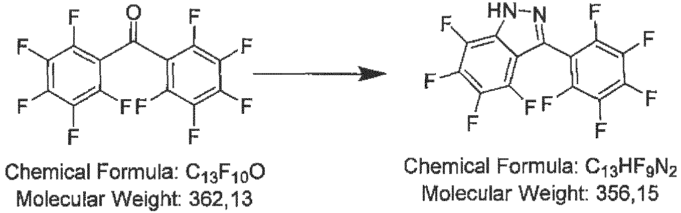
- 11.09 g (45.1 mmol) perfluoroacetophenone is dissolved in 100 mL toluene. The solution is cooled with an ice bath and 2.3 mL (2.37 g, 47.3 mmol, 1.05 eq) hydrazine-monohydrate is added dropwise. The mixture is heated to reflux for 3 days. After cooling to room temperature, the mixture is washed two times with 100 mL saturated aqueous sodium hydrogen carbonate solution and two times with 100 mL water, dried over magnesium sulfate and the solvent is removed under reduced pressure. The yellow, oily residue is distilled from bulb to bulb at a temperature about 140 °C and pressure about 12 Pa. The crude product is dissolved in hot hexane and the solution stored at -18 °C. The precipitated solid is filtered off and the slurry washed two times in 10 mL hexane. 5.0 g (43 %) product are obtained as a slightly yellow solid.
GCMS: confirms the expected M/z (mass/charge) ratio 258 -
- 5.1 g (19.8 mmol) 4,5,6,7-tetrafluoro-3-(trifluoromethyl)-1H-indazole is added under Ar counter-flow to an out-baked Schlenk flask and treated with 3 mL toluene. Freshly pulverized lithium borohydride is added to the starting material. The mixture is heated to 100 °C, until hydrogen formed ceases (ca. 4h). After slight cooling, 15 mL hexane are added, the mixture is heated to reflux for 10 min and cooled to room temperature. The precipitated solid is filtered off, washed with 10 mL hot hexane and dried in high vacuum. 2.55g (49 %) product is obtained as an off-white solid.
-

- 2.0 g ( 9.8 mmol, 5 eq) 3,5-bis(trifluoromethyl)pyrazole in a baked-out Schlenk flask is dissolved in 5 mL dry toluene. 43 mg (1.96 mmol, 1 eq) freshly pulverized lithium borohydride is added under Ar counter-flow and the mixture is heated to reflux for 3 days. The solvent and the excessive starting material are removed by distillation under reduced pressure and the residue is crystallized from n-chlorohexane. 0.25 g (20 %) product is obtained as a white solid.
-
GC-MS: confirms the expected M/z (mass/charge) ratio 356 -

- 1.02 g (2.86 mmol, 3.0 eq) 4,5,6,7-tetrafluoro-3-(perfluorophenyl)-1H-indazole are dissolved in 5 mL chlorobenzene in a baked-out Schlenk flask. Freshly pulverized lithium borohydride (21 mg, 0.95 mmol, 1.0 eq) is added under Ar counter-flow. The mixture is heated to 150 °C for 2 days and cooled to room temperature. The solvent is removed under reduced pressure and the residue dried in high vacuum. The crude is further purified by drying in a bulb to bulb apparatus at a temperature about 150 °C and a pressure about12 Pa. 0.57 g (70 %) product is obtained as an off-white solid.
-

- Freshly pulverized lithium borohydride (15 mg, 0.7 mmol, 1.0 eq) is placed in a baked-out pressure tube, 0.5 g (2.79 mmol, 4.0 eq) 5,6-difluoro-1H-indazole-3-carbonitrile are added under Ar counter-flow and washed down with 1 mL toluene. The pressure tube is closed and heated to a temperature about 160 °C for ca 21 h. After cooling to room temperature, the mixture is treated with 5 mL hexane in an ultra-sonic bath for
ca 30 min. The precipitated solid is filtered off and washed with hexane (20 mL in total). After drying, 0.48 g yellowish solid is obtained. -

- 0.57g (0.91 mmol) lithium tris(3,5-bis(trifluoromethyl)-1H-pyrazol-1-yl)hydroborate is dissolved in 6 mL N,N-dimethyl formamide. An aqueous solution of 62 mg zinc dichloride in 1 mL water is added dropwise. 20 mL water is further added and the mixture is treated in an ultra-sonic bath for 2 h. The precipitate is filtered off and dried in high vacuum. 0.485 g (82 %) product is obtained as a white solid.
- On a glass substrate provided with an ITO anode having thickness 90 nm, there were subsequently deposited 10 nm hole injection layer made of F1 doped with 8 wt% PD-2; 140 nm thick undoped hole transport layer made of neat F1; 20 nm thick first emitting layer formed of ABH113 doped with 3 wt% BD200 (both supplied by SFC, Korea); 25 nm thick first electron transport layer made of neat F2; 10 nm thick electron-generating part of the charge-generating layer (n-CGL) made of F3 doped with 5 wt% Yb; 2 nm thick interlayer made of F4; 30 nm thick hole-generating part of the charge-generating layer (p-CGL) made of PB-1; 10 nm thick second hole transport layer made of neat F1; 20 nm second emitting layer of the same thickness and composition as the first emitting layer; 25 nm thick first electron transport layer made of neat F2; 10 nm thick electron injection layer (EIL) made of F3 doped with 5 wt% Yb; 100 nm Al cathode.
- All layers were deposited by vacuum thermal evaporation (VTE).
- At the current density 10 mA/cm2, the operational voltage of the device 8 V was well comparable with the same device comprising a commercial state-of-art p-dopant instead of PB-1. Exact calibration of measuring equipment necessary for luminance/efficiency comparison was not made in this experiment..
- On the same glass substrate provided with an ITO anode as in the Example 1, following layers were subsequently deposited by VTE: 10 nm hole injection layer made of the compound PB-1; 120 nm thick HTL made of neat F1; 20 nm EML made of ABH113 doped with 3 wt% NUBD370 (both supplied by SFC, Korea), 36 nm EIL/ETL made of F2 doped with 50 wt% LiQ; 100 nm Al cathode.
- Comparative device comprised the HIL made of the compound CN-HAT (CAS 105598-27-4) instead of PB-1.
- The inventive device achieved current density 15 mA/cm2 and external quantum efficiency (EQE) 5.4 % at an operational voltage 5.2 V, whereas the comparative device exhibited the same current density at a significantly higher voltage 5.4 V and with a significantly lower EQE 4.9 %.
Table 1 auxiliary materials Compound Structure F1 
(CAS 1242056-42-3) F2 
(CAS 1440545-225-1) F3 
(CAS 597578-38-6) F4 
(CAS 1207671-22-4) PD2 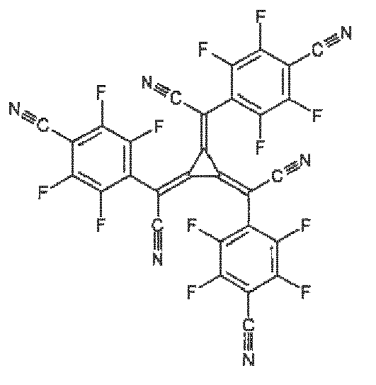
2,2',2"-(cyclopropane-1,2,3-triylidene)-tris[2-(4-cyanoperfluorophenyl)-acetonitrile] (CAS1224447-88-4) LiQ 
8-Hydroxyquinolato lithium (CAS 850918-68-2) CN-HAT 
(CAS 105598-27-4) - The features disclosed in the foregoing description and in the dependent claims may, both separately and in any combination thereof, be material for realizing the aspects of the disclosure made in the independent claims, in diverse forms thereof.
-
- CV
- cyclic voltammetry
- DSC
- differential scanning calorimentry
- EBL
- electron blocking layer
- EIL
- electron injecting layer
- EML
- emitting layer
- eq.
- equivalent
- ETL
- electron transport layer
- ETM
- electron transport matrix
- Fc
- ferrocene
- Fc+
- ferricenium
- HBL
- hole blocking layer
- HIL
- hole injecting layer
- HOMO
- highest occupied molecular orbital
- HPLC
- high performance liquid chromatography
- HTL
- hole transport layer
- p-HTL
- p-doped hole transport layer
- HTM
- hole transport matrix
- ITO
- indium tin oxide
- LUMO
- lowest unoccupied molecular orbital
- mol%
- molar percent
- NMR
- nuclear magnetic resonance
- OLED
- organic light emitting diode
- OPV
- organic photovoltaics
- QE
- quantum efficiency
- Rf
- retardation factor in TLC
- RGB
- red-green-blue
- TCO
- transparent conductive oxide
- TFT
- thin film transistor
- Tg
- glass transition temperature
- TLC
- thin layer chromatography
- wt%
- weight percent
Claims (21)
- Display device (1) comprising- a plurality of OLED pixels comprising at least two OLED pixels (2, 3, 4), the OLED pixels (2, 3, 4) comprising an anode (2a, 3a, 4a), a cathode (6), and a stack of organic layers, wherein the stack of organic layers- is arranged between and in contact with the cathode (6) and the anode (2a, 3a, 4a), and- comprises a first electron transport layer (9), a first hole transport layer (7), and a first light emitting layer provided between the first hole transport layer (7) and the first electron transport layer (9), and- a driving circuit configured to separately driving the pixels of the plurality of OLED pixels(2, 3, 4),wherein, for the plurality of OLED pixels(2, 3, 4), the first hole transport layer (7) is provided in the stack of organic layers as a common hole transport layer shared by the plurality of OLED pixels (2, 3, 4), and the first hole transport layer comprises(i) at least one first hole transport matrix compound consisting of covalently bound atoms and(ii) at least one electrical p-dopant characterized in that the electrical p-dopant is selected from metal salts and from electrically neutral metal complexes comprising a metal cation and at least one anion and/or at least one anionic ligand, wherein the anion and/or the anionic ligand consists of at least 5 covalently bound atoms, wherein the anion and/or anionic ligand comprises at least one atom selected from B, C, N,wherein the metal cation of the electrical p-dopant is selected from alkali metals; alkaline earth metals, Pb, Mn, Fe, Co, Ni, Zn, Cd; rare earth metals in oxidation state (II) or (III); Al, Ga, In; and from Sn, Ti, Zr, Hf, V, Nb, Ta, Cr, Mo and W in oxidation state (IV) or less.
- Display device (1) according to claim 1, wherein the anion and/or the anionic ligand consists of at least 6, more preferably at least 7, even more preferably at least 8, most preferably at least 9 covalently bound atoms.
- Display device (1) according to any of the preceding claims, wherein the anion and/or anionic ligand comprises at least two atoms selected from B, C and N which are bound to each other by a covalent bond.
- Display device (1) according to any of the preceding claims, wherein the anion and/or anionic ligand comprises at least one peripheral atom selected from H, N, O, F, Cl, Br and I.
- Display device (1) according to any of the preceding claims, wherein the anion and/or anionic ligand comprises at least one electron withdrawing group selected from halogenated alkyl, halogenated (hetero)aryl, halogenated (hetero)arylalkyl, halogenated alkylsulfonyl, halogenated (hetero)arylsulfonyl, halogenated (hetero)arylalkylsulfonyl, cyano.
- Display device (1) according to claim 5, wherein the electron withdrawing group is a perhalogenated group.
- Display device (1) according to claim 6, wherein the perhalogenated electron withdrawing group is a perfluorinated group.
- Display device (1) according to any of the preceding claims, wherein the metal cation of the p-dopant is selected from Li(I), Na(I), K(I), Rb(I), Cs(I); Mg(II), Ca(II), Sr(II), Ba(II), Sn(II), Pb(II), Mn(II), Fe(II), Co(II), Ni(II), Zn(II), Cd(II), Al(III); rare earth metal in oxidation state (III), V(III), Nb(III), Ta(III), Cr(III), Mo(III), W(III) Ga(III), In(III) and from Ti(IV), Zr(IV), Hf(IV), Sn(IV).
- Display device (1) according to any of the preceding claims, wherein in the p-dopant molecule, the atom of the anion and/or of the anionic ligand which is closest to the metal cation is a C or a N atom.
- Display device (1) according to any of the preceding claims, wherein the acidity of the electrically neutral conjugated acid formed from the anion and/or anionic ligand by addition of one or more protons in 1,2-dichloroethane is higher than that of HCl, preferably higher than that of HBr, more preferably higher than that of HI, even more preferably higher than that of fluorosulfuric acid, and most preferably higher than that of perchloric acid, wherein the measurement of the acidity in 1,2-dichlorethane is performed in line with the disclosure of Journal of Organic Chemistry (2011), 76(2), 391-395.
- Display device (1) according to any of the preceding claims, wherein the electrical p-dopant has energy level of its highest unoccupied molecular orbital computed by standard quantum chemical method and expressed in absolute vacuum scale at least 0.5 eV, preferably at least 0.6 eV, more preferably at least 0.8 eV, even more preferably at least 1.0 eV, most preferably at least 1.2 eV above the energy level of the highest occupied orbital of the first hole transport matrix compound computed by the standard quantum chemical method, wherein the standard quantum chemical method uses the software package TURBOMOLE using DFT functional B3LYP with the basis set def2-TZVP.
- Display device (1) according to any of the preceding claims, wherein the first hole transport matrix compound is an organic compound, preferably an organic compound comprising a conjugated system of at least 6, more preferably at least 10 delocalized electrons; also preferably, the first hole transport matrix compound comprises at least one triaryl amine structural moiety, more preferably, the first hole transport matrix compound comprises at least two triaryl amine structural moieties.
- Method for preparing the display device (1) according to any of the preceding claims, the method comprising at least one step wherein the first hole transport matrix compound and the electrical p-dopant are in mutual contact exposed to a temperature above 50 °C.
- Method according to claim 13, wherein(i) the p-dopant and the first hole transport matrix compound are dispersed in a solvent,(ii) the dispersion is deposited on a substrate and(iii) the solvent is evaporated at an elevated temperature.
- Method according to claim 13, further comprising at least one step wherein the p-dopant is evaporated at a reduced pressure, preferably at a pressure below 1×10⁻² Pa and at a temperature above 50 °C, more preferably at a pressure below 5×10⁻² Pa and at a temperature above 80 °C, even more preferably at a pressure below 1×10⁻³ Pa and at a temperature above 120 °C, most preferably at a pressure below 5×10⁻⁴ Pa and at a temperature above 150 °C.
- Method according to claim 13 to 15, wherein the p-dopant is used in form of a solid hydrate.
- Method according to claim 15, wherein the p-dopant is used as an anhydrous solid comprising less than 0.10 wt % water, preferably less than 0.05 wt % water.
- Compound having formula (I)
 Mx⊕ is a x-valent cation of a metal selected from alkali metals, alkaline earth metals, rare earth metals and Al, Ga, In, Sn, Ti, Zr, Hf, V, Nb, Ta, Cr, Mo, W, Mn, Fe, Co, Ni, Zn and Cd;x is 1 for M selected from alkali metals; 2 for M selected from alkaline earth metals, Mn, Fe, Co, Ni, Zn and Cd; 2 or 3 for M selected from rare earth metals; 3 for Al, Ga, In; 2, 3 or 4 for Ti, Zr, Hf, V, Nb, Ta, Cr, Mo, W; and 2 or 4 for Sn;B1and B2 is independently selected from perhalogenated C3 to C20 alkyl, C3 to C20 cycloalkyl or C3 to C20 arylalkyl;with the proviso that the compound having formula (I), whereina) M is selected from alkali metals, Mg, Ca and Zn and B1 and B2 are independently selected from perfluorinated straight-chain primary alkyl, orb) M is Li and B1 and B2 is perfluorinated isopropyl,is excluded.
 - Compound according to claim 18, wherein M is selected from Mg(II), Mn(II) and Zn(II).
- Compound according to claim 18 or 19 in a solid form, preferably in a solid form comprising less than 0.10 wt % water, more preferably in a solid form comprising less than 0.05 wt % water, most preferably in a solid crystalline form comprising less than 0.05 wt % water.
- Compound according to claim 18 or 19 in form of a solid crystalline hydrate, preferably in form of a solid crystalline hydrate which has water content in the range(i) from 30.33 to 36.33 mol%, preferably from 31.00 to 35.66 mol%, more preferably from 31.00 to 35.66 mol%, even more preferably from 31.66 to 35.00 mol%, even more preferably from 32.33 to 34.33 mol%, most preferably from 33.00 to 33.66 mol%; or(ii) from 18.20 to 21.80 mol%, preferably from 18.60 to 21.40 mol%, more preferably from 19.00 to 21.00 mol%, even more preferably from 19.40 to 20.60 mol%, most preferably from 19.80 to 20.20 mol%.
Priority Applications (45)
| Application Number | Priority Date | Filing Date | Title |
|---|---|---|---|
| EP17156902.3A EP3364476B1 (en) | 2017-02-20 | 2017-02-20 | Active oled display, method for preparing an active oled display and compound |
| JP2019545368A JP7082984B2 (en) | 2017-02-20 | 2018-02-16 | Electronic semiconductor devices and manufacturing methods and compounds for the electronic semiconductor devices |
| US16/485,824 US11539014B2 (en) | 2017-02-20 | 2018-02-16 | Electronic semiconducting device, method for preparing the electronic semiconducting device and compound |
| CN201880012552.0A CN110447117B (en) | 2017-02-20 | 2018-02-16 | Electronic semiconductor device, preparation method and compound of electronic semiconductor device |
| KR1020197027314A KR102478039B1 (en) | 2017-02-20 | 2018-02-16 | Electronic semiconducting elements, methods and compounds for making electronic semiconducting elements |
| EP18704265.0A EP3583636B1 (en) | 2017-02-20 | 2018-02-16 | Electronic semiconducting device, method for preparing the electronic semiconducting device and compound |
| PCT/EP2018/053954 WO2018150006A1 (en) | 2017-02-20 | 2018-02-16 | Electronic semiconducting device, method for preparing the electronic semiconducting device and compound |
| CN201880012559.2A CN110462871B (en) | 2017-02-20 | 2018-02-20 | Electronic semiconductor device and method for producing said electronic semiconductor device |
| US16/485,839 US11201306B2 (en) | 2017-02-20 | 2018-02-20 | Active OLED display, method for preparing an active OLED display and compound |
| US16/485,816 US11322710B2 (en) | 2017-02-20 | 2018-02-20 | Electronic semiconducting device and method for preparing the electronic semiconducting device |
| DE112018000907.6T DE112018000907B4 (en) | 2017-02-20 | 2018-02-20 | Electronic semiconductor device and method for manufacturing the electronic semiconductor device |
| CN201880012813.9A CN110521014B (en) | 2017-02-20 | 2018-02-20 | Electronic semiconductor device and method of making electronic semiconductor device |
| EP18706500.8A EP3583638B1 (en) | 2017-02-20 | 2018-02-20 | Electronic semiconducting device and method for preparing the electronic semiconducting device |
| DE112018000908.4T DE112018000908B4 (en) | 2017-02-20 | 2018-02-20 | Electronic device, method for manufacturing the same and display device comprising the same |
| PCT/EP2018/054154 WO2018150048A1 (en) | 2017-02-20 | 2018-02-20 | Electronic semiconducting device and method for preparing the electronic sem-iconducting device |
| JP2019545350A JP2020508580A (en) | 2017-02-20 | 2018-02-20 | Active OLED display, method of manufacturing active OLED display and compound |
| CN201880012814.3A CN110462872B (en) | 2017-02-20 | 2018-02-20 | Electronic device, method of manufacturing the same, and display device including the same |
| PCT/EP2018/054162 WO2018150051A1 (en) | 2017-02-20 | 2018-02-20 | Electronic semiconducting device and method for preparing the electronic semiconducting device |
| EP22171384.5A EP4057369B1 (en) | 2017-02-20 | 2018-02-20 | Active oled display, method for preparing an active oled display and compound |
| KR1020197027280A KR102519014B1 (en) | 2017-02-20 | 2018-02-20 | Electronic semiconducting elements and methods for manufacturing electronic semiconducting elements |
| JP2019544850A JP7305544B2 (en) | 2017-02-20 | 2018-02-20 | Electronic semiconductor device and manufacturing method thereof |
| JP2019544861A JP7373994B2 (en) | 2017-02-20 | 2018-02-20 | Electronic semiconductor device and its manufacturing method |
| CN202211016963.1A CN115377309A (en) | 2017-02-20 | 2018-02-20 | Active OLED display, method and compound for producing active OLED display |
| KR1020197027327A KR102690851B1 (en) | 2017-02-20 | 2018-02-20 | Active OLED displays, methods and compounds for manufacturing active OLED displays |
| EP25195136.4A EP4629808A3 (en) | 2017-02-20 | 2018-02-20 | Electronic semiconducting device and method for preparing the electronic semiconducting device |
| CN202210672671.7A CN115241374A (en) | 2017-02-20 | 2018-02-20 | Electronic semiconductor device and method for producing said electronic semiconductor device |
| US16/485,808 US11239440B2 (en) | 2017-02-20 | 2018-02-20 | Electronic semiconducting device and method for preparing the electronic semiconducting device |
| US16/485,813 US11522150B2 (en) | 2017-02-20 | 2018-02-20 | Electronic device, method for preparing the same and display device comprising the same |
| JP2019544860A JP6999684B2 (en) | 2017-02-20 | 2018-02-20 | An electronic device, a method for manufacturing the electronic device, and a display device containing the electronic device. |
| KR1020197027323A KR102677446B1 (en) | 2017-02-20 | 2018-02-20 | Electronic semiconducting devices and methods for manufacturing electronic semiconducting devices |
| CN201880013739.2A CN110521015B (en) | 2017-02-20 | 2018-02-20 | Active OLED display, method and compound for making active OLED display |
| EP18706499.3A EP3583637B1 (en) | 2017-02-20 | 2018-02-20 | Active oled display, method for preparing an active oled display and compound |
| PCT/EP2018/054160 WO2018150050A1 (en) | 2017-02-20 | 2018-02-20 | Active oled display, method for preparing an active oled display and compound |
| PCT/EP2018/054157 WO2018150049A1 (en) | 2017-02-20 | 2018-02-20 | Electronic device, method for preparing the same and display device comprising the same |
| KR1020197027288A KR102516665B1 (en) | 2017-02-20 | 2018-02-20 | Electronic device, method for manufacturing the same, and display device including the same |
| KR1020247025441A KR20240119182A (en) | 2017-02-20 | 2018-02-20 | Active OLED display, method for preparing an active OLED display and compound |
| TW107105851A TWI806851B (en) | 2017-02-20 | 2018-02-21 | Active oled display and method for preparing an active oled display |
| TW107105850A TWI761457B (en) | 2017-02-20 | 2018-02-21 | Electronic semiconducting device and method for preparing the electronic semiconducting device |
| TW107105848A TWI762586B (en) | 2017-02-20 | 2018-02-21 | Electronic semiconducting device and method for preparing the electronic semiconducting device |
| TW107105849A TWI753111B (en) | 2017-02-20 | 2018-02-21 | Electronic device, method for preparing the same and display device comprising the same |
| US17/519,446 US20220059787A1 (en) | 2017-02-20 | 2021-11-04 | Active OLED Display, Method for Preparing an Active OLED Display and Compound |
| US17/659,565 US11825667B2 (en) | 2017-02-20 | 2022-04-18 | Electronic semiconducting device and method for preparing the electronic semiconducting device |
| US17/881,878 US12022672B2 (en) | 2017-02-20 | 2022-08-05 | Electronic semiconducting device, method for preparing the electronic semiconducting device and compound |
| JP2022144426A JP7447209B2 (en) | 2017-02-20 | 2022-09-12 | Active OLED display, active OLED display manufacturing method and compound |
| JP2022178073A JP7541563B2 (en) | 2017-02-20 | 2022-11-07 | Electronic semiconductor device and method of manufacturing same |
Applications Claiming Priority (1)
| Application Number | Priority Date | Filing Date | Title |
|---|---|---|---|
| EP17156902.3A EP3364476B1 (en) | 2017-02-20 | 2017-02-20 | Active oled display, method for preparing an active oled display and compound |
Publications (2)
| Publication Number | Publication Date |
|---|---|
| EP3364476A1 EP3364476A1 (en) | 2018-08-22 |
| EP3364476B1 true EP3364476B1 (en) | 2024-06-05 |
Family
ID=58094304
Family Applications (1)
| Application Number | Title | Priority Date | Filing Date |
|---|---|---|---|
| EP17156902.3A Active EP3364476B1 (en) | 2017-02-20 | 2017-02-20 | Active oled display, method for preparing an active oled display and compound |
Country Status (1)
| Country | Link |
|---|---|
| EP (1) | EP3364476B1 (en) |
Families Citing this family (4)
| Publication number | Priority date | Publication date | Assignee | Title |
|---|---|---|---|---|
| JP7082984B2 (en) | 2017-02-20 | 2022-06-09 | ノヴァレッド ゲーエムベーハー | Electronic semiconductor devices and manufacturing methods and compounds for the electronic semiconductor devices |
| EP4106027B1 (en) * | 2021-06-18 | 2025-12-31 | Novaled GmbH | OLED DISPLAY WITH ACTIVE MATRIX |
| EP4106030B1 (en) * | 2021-06-18 | 2025-12-31 | Novaled GmbH | SURFACE RESISTANCE COMPONENT |
| EP4106031A1 (en) * | 2021-06-18 | 2022-12-21 | Novaled GmbH | Sheet resistance component |
Citations (2)
| Publication number | Priority date | Publication date | Assignee | Title |
|---|---|---|---|---|
| EP0510541A1 (en) * | 1991-04-19 | 1992-10-28 | Mitsubishi Chemical Corporation | Organic elecroluminescent device |
| JP2010087276A (en) * | 2008-09-30 | 2010-04-15 | Toshiba Mobile Display Co Ltd | Display device |
Family Cites Families (12)
| Publication number | Priority date | Publication date | Assignee | Title |
|---|---|---|---|---|
| DE102007012794B3 (en) | 2007-03-16 | 2008-06-19 | Novaled Ag | Pyrido [3,2-h] quinazolines and / or their 5,6-dihydro derivatives, their method of preparation and doped organic semiconductor material containing them |
| CN102892859B (en) | 2010-04-27 | 2016-03-09 | 诺瓦莱德公开股份有限公司 | Organic semiconductor material and electronic component |
| JP2014517807A (en) * | 2011-02-25 | 2014-07-24 | エコール ポリテクニーク フェデラル ドゥ ローザンヌ(エーペーエフエル) | Metal complexes for use as dopants and other uses |
| TWI526418B (en) | 2011-03-01 | 2016-03-21 | 諾瓦發光二極體股份公司 | Organic semiconductor materials and organic compositions |
| TWI584513B (en) | 2011-11-30 | 2017-05-21 | 諾瓦發光二極體有限公司 | Display |
| TW201341347A (en) | 2012-03-15 | 2013-10-16 | Novaled Ag | Aromatic amine terphenyl compounds and their applications in organic semiconductor devices |
| EP2722908A1 (en) | 2012-10-17 | 2014-04-23 | Novaled AG | Phosphorescent OLED and hole transporting materials for phosphorescent OLEDs |
| KR102035251B1 (en) * | 2013-03-12 | 2019-10-23 | 삼성디스플레이 주식회사 | Organic light emitting diode display |
| EP3002797B1 (en) * | 2014-09-30 | 2020-04-29 | Novaled GmbH | A light emitting organic device and an active OLED display |
| US20180201800A1 (en) * | 2015-07-17 | 2018-07-19 | Nissan Chemical Industries, Ltd. | Non-aqueous ink compositions containing metalloid nanoparticles suitable for use in organic electronics |
| EP3133664A1 (en) * | 2015-08-18 | 2017-02-22 | Novaled GmbH | Triaryl amine thick layer doped with metal amides for use as hole injection layer for an organic light-emitting diode (oled) |
| EP3133663B1 (en) * | 2015-08-18 | 2022-06-15 | Novaled GmbH | Metal amides for use as hole injection layer for an organic light-emitting diode (oled) |
-
2017
- 2017-02-20 EP EP17156902.3A patent/EP3364476B1/en active Active
Patent Citations (2)
| Publication number | Priority date | Publication date | Assignee | Title |
|---|---|---|---|---|
| EP0510541A1 (en) * | 1991-04-19 | 1992-10-28 | Mitsubishi Chemical Corporation | Organic elecroluminescent device |
| JP2010087276A (en) * | 2008-09-30 | 2010-04-15 | Toshiba Mobile Display Co Ltd | Display device |
Also Published As
| Publication number | Publication date |
|---|---|
| EP3364476A1 (en) | 2018-08-22 |
Similar Documents
| Publication | Publication Date | Title |
|---|---|---|
| US11825667B2 (en) | Electronic semiconducting device and method for preparing the electronic semiconducting device | |
| EP3364476B1 (en) | Active oled display, method for preparing an active oled display and compound | |
| EP3364477A1 (en) | Electronic semiconducting device and method for preparing the electronic semiconducting device | |
| EP3364475B1 (en) | Electronic semiconducting device, method for preparing the electronic semiconducting device and compound |
Legal Events
| Date | Code | Title | Description |
|---|---|---|---|
| PUAI | Public reference made under article 153(3) epc to a published international application that has entered the european phase |
Free format text: ORIGINAL CODE: 0009012 |
|
| STAA | Information on the status of an ep patent application or granted ep patent |
Free format text: STATUS: REQUEST FOR EXAMINATION WAS MADE |
|
| 17P | Request for examination filed |
Effective date: 20180309 |
|
| AK | Designated contracting states |
Kind code of ref document: A1 Designated state(s): AL AT BE BG CH CY CZ DE DK EE ES FI FR GB GR HR HU IE IS IT LI LT LU LV MC MK MT NL NO PL PT RO RS SE SI SK SM TR |
|
| AX | Request for extension of the european patent |
Extension state: BA ME |
|
| RAP1 | Party data changed (applicant data changed or rights of an application transferred) |
Owner name: NOVALED GMBH |
|
| STAA | Information on the status of an ep patent application or granted ep patent |
Free format text: STATUS: EXAMINATION IS IN PROGRESS |
|
| 17Q | First examination report despatched |
Effective date: 20200226 |
|
| REG | Reference to a national code |
Ref country code: DE Ref legal event code: R079 Free format text: PREVIOUS MAIN CLASS: H01L0051540000 Ipc: H10K0050155000 Ref country code: DE Ref legal event code: R079 Ref document number: 602017082379 Country of ref document: DE Free format text: PREVIOUS MAIN CLASS: H01L0051540000 Ipc: H10K0050155000 |
|
| GRAP | Despatch of communication of intention to grant a patent |
Free format text: ORIGINAL CODE: EPIDOSNIGR1 |
|
| STAA | Information on the status of an ep patent application or granted ep patent |
Free format text: STATUS: GRANT OF PATENT IS INTENDED |
|
| RIC1 | Information provided on ipc code assigned before grant |
Ipc: H10K 85/30 20230101ALI20231208BHEP Ipc: H10K 59/35 20230101ALI20231208BHEP Ipc: H10K 50/155 20230101AFI20231208BHEP |
|
| INTG | Intention to grant announced |
Effective date: 20240108 |
|
| GRAS | Grant fee paid |
Free format text: ORIGINAL CODE: EPIDOSNIGR3 |
|
| GRAA | (expected) grant |
Free format text: ORIGINAL CODE: 0009210 |
|
| STAA | Information on the status of an ep patent application or granted ep patent |
Free format text: STATUS: THE PATENT HAS BEEN GRANTED |
|
| AK | Designated contracting states |
Kind code of ref document: B1 Designated state(s): AL AT BE BG CH CY CZ DE DK EE ES FI FR GB GR HR HU IE IS IT LI LT LU LV MC MK MT NL NO PL PT RO RS SE SI SK SM TR |
|
| REG | Reference to a national code |
Ref country code: GB Ref legal event code: FG4D |
|
| P01 | Opt-out of the competence of the unified patent court (upc) registered |
Effective date: 20240506 |
|
| REG | Reference to a national code |
Ref country code: CH Ref legal event code: EP |
|
| REG | Reference to a national code |
Ref country code: DE Ref legal event code: R096 Ref document number: 602017082379 Country of ref document: DE |
|
| REG | Reference to a national code |
Ref country code: IE Ref legal event code: FG4D |
|
| REG | Reference to a national code |
Ref country code: LT Ref legal event code: MG9D |
|
| PG25 | Lapsed in a contracting state [announced via postgrant information from national office to epo] |
Ref country code: BG Free format text: LAPSE BECAUSE OF FAILURE TO SUBMIT A TRANSLATION OF THE DESCRIPTION OR TO PAY THE FEE WITHIN THE PRESCRIBED TIME-LIMIT Effective date: 20240605 |
|
| REG | Reference to a national code |
Ref country code: NL Ref legal event code: MP Effective date: 20240605 |
|
| PG25 | Lapsed in a contracting state [announced via postgrant information from national office to epo] |
Ref country code: FI Free format text: LAPSE BECAUSE OF FAILURE TO SUBMIT A TRANSLATION OF THE DESCRIPTION OR TO PAY THE FEE WITHIN THE PRESCRIBED TIME-LIMIT Effective date: 20240605 Ref country code: HR Free format text: LAPSE BECAUSE OF FAILURE TO SUBMIT A TRANSLATION OF THE DESCRIPTION OR TO PAY THE FEE WITHIN THE PRESCRIBED TIME-LIMIT Effective date: 20240605 |
|
| PG25 | Lapsed in a contracting state [announced via postgrant information from national office to epo] |
Ref country code: GR Free format text: LAPSE BECAUSE OF FAILURE TO SUBMIT A TRANSLATION OF THE DESCRIPTION OR TO PAY THE FEE WITHIN THE PRESCRIBED TIME-LIMIT Effective date: 20240906 |
|
| PG25 | Lapsed in a contracting state [announced via postgrant information from national office to epo] |
Ref country code: ES Free format text: LAPSE BECAUSE OF FAILURE TO SUBMIT A TRANSLATION OF THE DESCRIPTION OR TO PAY THE FEE WITHIN THE PRESCRIBED TIME-LIMIT Effective date: 20240605 |
|
| PG25 | Lapsed in a contracting state [announced via postgrant information from national office to epo] |
Ref country code: LV Free format text: LAPSE BECAUSE OF FAILURE TO SUBMIT A TRANSLATION OF THE DESCRIPTION OR TO PAY THE FEE WITHIN THE PRESCRIBED TIME-LIMIT Effective date: 20240605 |
|
| PG25 | Lapsed in a contracting state [announced via postgrant information from national office to epo] |
Ref country code: NO Free format text: LAPSE BECAUSE OF FAILURE TO SUBMIT A TRANSLATION OF THE DESCRIPTION OR TO PAY THE FEE WITHIN THE PRESCRIBED TIME-LIMIT Effective date: 20240905 Ref country code: LV Free format text: LAPSE BECAUSE OF FAILURE TO SUBMIT A TRANSLATION OF THE DESCRIPTION OR TO PAY THE FEE WITHIN THE PRESCRIBED TIME-LIMIT Effective date: 20240605 Ref country code: HR Free format text: LAPSE BECAUSE OF FAILURE TO SUBMIT A TRANSLATION OF THE DESCRIPTION OR TO PAY THE FEE WITHIN THE PRESCRIBED TIME-LIMIT Effective date: 20240605 Ref country code: GR Free format text: LAPSE BECAUSE OF FAILURE TO SUBMIT A TRANSLATION OF THE DESCRIPTION OR TO PAY THE FEE WITHIN THE PRESCRIBED TIME-LIMIT Effective date: 20240906 Ref country code: FI Free format text: LAPSE BECAUSE OF FAILURE TO SUBMIT A TRANSLATION OF THE DESCRIPTION OR TO PAY THE FEE WITHIN THE PRESCRIBED TIME-LIMIT Effective date: 20240605 Ref country code: ES Free format text: LAPSE BECAUSE OF FAILURE TO SUBMIT A TRANSLATION OF THE DESCRIPTION OR TO PAY THE FEE WITHIN THE PRESCRIBED TIME-LIMIT Effective date: 20240605 Ref country code: BG Free format text: LAPSE BECAUSE OF FAILURE TO SUBMIT A TRANSLATION OF THE DESCRIPTION OR TO PAY THE FEE WITHIN THE PRESCRIBED TIME-LIMIT Effective date: 20240605 Ref country code: RS Free format text: LAPSE BECAUSE OF FAILURE TO SUBMIT A TRANSLATION OF THE DESCRIPTION OR TO PAY THE FEE WITHIN THE PRESCRIBED TIME-LIMIT Effective date: 20240905 |
|
| PG25 | Lapsed in a contracting state [announced via postgrant information from national office to epo] |
Ref country code: NL Free format text: LAPSE BECAUSE OF FAILURE TO SUBMIT A TRANSLATION OF THE DESCRIPTION OR TO PAY THE FEE WITHIN THE PRESCRIBED TIME-LIMIT Effective date: 20240605 |
|
| REG | Reference to a national code |
Ref country code: AT Ref legal event code: MK05 Ref document number: 1693380 Country of ref document: AT Kind code of ref document: T Effective date: 20240605 |
|
| PG25 | Lapsed in a contracting state [announced via postgrant information from national office to epo] |
Ref country code: NL Free format text: LAPSE BECAUSE OF FAILURE TO SUBMIT A TRANSLATION OF THE DESCRIPTION OR TO PAY THE FEE WITHIN THE PRESCRIBED TIME-LIMIT Effective date: 20240605 |
|
| PG25 | Lapsed in a contracting state [announced via postgrant information from national office to epo] |
Ref country code: PT Free format text: LAPSE BECAUSE OF FAILURE TO SUBMIT A TRANSLATION OF THE DESCRIPTION OR TO PAY THE FEE WITHIN THE PRESCRIBED TIME-LIMIT Effective date: 20241007 |
|
| PG25 | Lapsed in a contracting state [announced via postgrant information from national office to epo] |
Ref country code: PT Free format text: LAPSE BECAUSE OF FAILURE TO SUBMIT A TRANSLATION OF THE DESCRIPTION OR TO PAY THE FEE WITHIN THE PRESCRIBED TIME-LIMIT Effective date: 20241007 |
|
| PG25 | Lapsed in a contracting state [announced via postgrant information from national office to epo] |
Ref country code: PL Free format text: LAPSE BECAUSE OF FAILURE TO SUBMIT A TRANSLATION OF THE DESCRIPTION OR TO PAY THE FEE WITHIN THE PRESCRIBED TIME-LIMIT Effective date: 20240605 |
|
| PG25 | Lapsed in a contracting state [announced via postgrant information from national office to epo] |
Ref country code: EE Free format text: LAPSE BECAUSE OF FAILURE TO SUBMIT A TRANSLATION OF THE DESCRIPTION OR TO PAY THE FEE WITHIN THE PRESCRIBED TIME-LIMIT Effective date: 20240605 |
|
| PG25 | Lapsed in a contracting state [announced via postgrant information from national office to epo] |
Ref country code: IS Free format text: LAPSE BECAUSE OF FAILURE TO SUBMIT A TRANSLATION OF THE DESCRIPTION OR TO PAY THE FEE WITHIN THE PRESCRIBED TIME-LIMIT Effective date: 20241005 Ref country code: AT Free format text: LAPSE BECAUSE OF FAILURE TO SUBMIT A TRANSLATION OF THE DESCRIPTION OR TO PAY THE FEE WITHIN THE PRESCRIBED TIME-LIMIT Effective date: 20240605 |
|
| PG25 | Lapsed in a contracting state [announced via postgrant information from national office to epo] |
Ref country code: CZ Free format text: LAPSE BECAUSE OF FAILURE TO SUBMIT A TRANSLATION OF THE DESCRIPTION OR TO PAY THE FEE WITHIN THE PRESCRIBED TIME-LIMIT Effective date: 20240605 |
|
| PG25 | Lapsed in a contracting state [announced via postgrant information from national office to epo] |
Ref country code: SK Free format text: LAPSE BECAUSE OF FAILURE TO SUBMIT A TRANSLATION OF THE DESCRIPTION OR TO PAY THE FEE WITHIN THE PRESCRIBED TIME-LIMIT Effective date: 20240605 Ref country code: RO Free format text: LAPSE BECAUSE OF FAILURE TO SUBMIT A TRANSLATION OF THE DESCRIPTION OR TO PAY THE FEE WITHIN THE PRESCRIBED TIME-LIMIT Effective date: 20240605 |
|
| PG25 | Lapsed in a contracting state [announced via postgrant information from national office to epo] |
Ref country code: SM Free format text: LAPSE BECAUSE OF FAILURE TO SUBMIT A TRANSLATION OF THE DESCRIPTION OR TO PAY THE FEE WITHIN THE PRESCRIBED TIME-LIMIT Effective date: 20240605 |
|
| PG25 | Lapsed in a contracting state [announced via postgrant information from national office to epo] |
Ref country code: SM Free format text: LAPSE BECAUSE OF FAILURE TO SUBMIT A TRANSLATION OF THE DESCRIPTION OR TO PAY THE FEE WITHIN THE PRESCRIBED TIME-LIMIT Effective date: 20240605 Ref country code: SK Free format text: LAPSE BECAUSE OF FAILURE TO SUBMIT A TRANSLATION OF THE DESCRIPTION OR TO PAY THE FEE WITHIN THE PRESCRIBED TIME-LIMIT Effective date: 20240605 Ref country code: RO Free format text: LAPSE BECAUSE OF FAILURE TO SUBMIT A TRANSLATION OF THE DESCRIPTION OR TO PAY THE FEE WITHIN THE PRESCRIBED TIME-LIMIT Effective date: 20240605 Ref country code: PL Free format text: LAPSE BECAUSE OF FAILURE TO SUBMIT A TRANSLATION OF THE DESCRIPTION OR TO PAY THE FEE WITHIN THE PRESCRIBED TIME-LIMIT Effective date: 20240605 Ref country code: IS Free format text: LAPSE BECAUSE OF FAILURE TO SUBMIT A TRANSLATION OF THE DESCRIPTION OR TO PAY THE FEE WITHIN THE PRESCRIBED TIME-LIMIT Effective date: 20241005 Ref country code: EE Free format text: LAPSE BECAUSE OF FAILURE TO SUBMIT A TRANSLATION OF THE DESCRIPTION OR TO PAY THE FEE WITHIN THE PRESCRIBED TIME-LIMIT Effective date: 20240605 Ref country code: CZ Free format text: LAPSE BECAUSE OF FAILURE TO SUBMIT A TRANSLATION OF THE DESCRIPTION OR TO PAY THE FEE WITHIN THE PRESCRIBED TIME-LIMIT Effective date: 20240605 Ref country code: AT Free format text: LAPSE BECAUSE OF FAILURE TO SUBMIT A TRANSLATION OF THE DESCRIPTION OR TO PAY THE FEE WITHIN THE PRESCRIBED TIME-LIMIT Effective date: 20240605 |
|
| PG25 | Lapsed in a contracting state [announced via postgrant information from national office to epo] |
Ref country code: IT Free format text: LAPSE BECAUSE OF FAILURE TO SUBMIT A TRANSLATION OF THE DESCRIPTION OR TO PAY THE FEE WITHIN THE PRESCRIBED TIME-LIMIT Effective date: 20240605 |
|
| REG | Reference to a national code |
Ref country code: DE Ref legal event code: R097 Ref document number: 602017082379 Country of ref document: DE |
|
| PGFP | Annual fee paid to national office [announced via postgrant information from national office to epo] |
Ref country code: DE Payment date: 20241224 Year of fee payment: 9 |
|
| PLBE | No opposition filed within time limit |
Free format text: ORIGINAL CODE: 0009261 |
|
| STAA | Information on the status of an ep patent application or granted ep patent |
Free format text: STATUS: NO OPPOSITION FILED WITHIN TIME LIMIT |
|
| PG25 | Lapsed in a contracting state [announced via postgrant information from national office to epo] |
Ref country code: DK Free format text: LAPSE BECAUSE OF FAILURE TO SUBMIT A TRANSLATION OF THE DESCRIPTION OR TO PAY THE FEE WITHIN THE PRESCRIBED TIME-LIMIT Effective date: 20240605 |
|
| PGFP | Annual fee paid to national office [announced via postgrant information from national office to epo] |
Ref country code: GB Payment date: 20250102 Year of fee payment: 9 |
|
| 26N | No opposition filed |
Effective date: 20250306 |
|
| PG25 | Lapsed in a contracting state [announced via postgrant information from national office to epo] |
Ref country code: SE Free format text: LAPSE BECAUSE OF FAILURE TO SUBMIT A TRANSLATION OF THE DESCRIPTION OR TO PAY THE FEE WITHIN THE PRESCRIBED TIME-LIMIT Effective date: 20240605 |
|
| PG25 | Lapsed in a contracting state [announced via postgrant information from national office to epo] |
Ref country code: MC Free format text: LAPSE BECAUSE OF FAILURE TO SUBMIT A TRANSLATION OF THE DESCRIPTION OR TO PAY THE FEE WITHIN THE PRESCRIBED TIME-LIMIT Effective date: 20240605 |
|
| REG | Reference to a national code |
Ref country code: CH Ref legal event code: PL |
|
| PG25 | Lapsed in a contracting state [announced via postgrant information from national office to epo] |
Ref country code: LU Free format text: LAPSE BECAUSE OF NON-PAYMENT OF DUE FEES Effective date: 20250220 |
|
| PG25 | Lapsed in a contracting state [announced via postgrant information from national office to epo] |
Ref country code: CH Free format text: LAPSE BECAUSE OF NON-PAYMENT OF DUE FEES Effective date: 20250228 |
|
| REG | Reference to a national code |
Ref country code: BE Ref legal event code: MM Effective date: 20250228 |
|
| PGFP | Annual fee paid to national office [announced via postgrant information from national office to epo] |
Ref country code: FR Payment date: 20251208 Year of fee payment: 10 |
|
| PG25 | Lapsed in a contracting state [announced via postgrant information from national office to epo] |
Ref country code: BE Free format text: LAPSE BECAUSE OF NON-PAYMENT OF DUE FEES Effective date: 20250228 |
|
| PG25 | Lapsed in a contracting state [announced via postgrant information from national office to epo] |
Ref country code: IE Free format text: LAPSE BECAUSE OF NON-PAYMENT OF DUE FEES Effective date: 20250220 |