EP3319165A1 - A radio frequency reflection type phase shifter, and method of phase shifting - Google Patents
A radio frequency reflection type phase shifter, and method of phase shifting Download PDFInfo
- Publication number
- EP3319165A1 EP3319165A1 EP16306453.8A EP16306453A EP3319165A1 EP 3319165 A1 EP3319165 A1 EP 3319165A1 EP 16306453 A EP16306453 A EP 16306453A EP 3319165 A1 EP3319165 A1 EP 3319165A1
- Authority
- EP
- European Patent Office
- Prior art keywords
- radio frequency
- phase shifter
- reflection type
- variable capacitors
- frequency reflection
- Prior art date
- Legal status (The legal status is an assumption and is not a legal conclusion. Google has not performed a legal analysis and makes no representation as to the accuracy of the status listed.)
- Granted
Links
Images


Classifications
-
- H—ELECTRICITY
- H01—ELECTRIC ELEMENTS
- H01P—WAVEGUIDES; RESONATORS, LINES, OR OTHER DEVICES OF THE WAVEGUIDE TYPE
- H01P1/00—Auxiliary devices
- H01P1/18—Phase-shifters
- H01P1/184—Strip line phase-shifters
Definitions
- the present invention relates to a Radio Frequency reflection type phase shifter, and a method of Radio Frequency reflection type phase shifting.
- An example of the present invention is a Radio Frequency reflection type phase shifter, the phase shifter comprising a coupler for input and output, and N variable capacitors, where N is an integer value of 2 or more, each of the variable capacitors providing radio frequency reflection, each of the variable capacitors being connected to the coupler by at least one of the impedance transformers, the characteristic impedances of the impedance transformers having been selected so that the phase shifter provides a phase shift at least substantially proportional to the value of N, wherein each of the variable capacitors comprises electrochromic material.
- each of the variable capacitors comprises an electrolyte element and at least one electrochromic element between a first electrode and a second electrode.
- the first electrode comprises a ground plate on which lies the first electrochromic element, and the electrolyte element lies on the electrochromic element, the electrochromic element comprising an electrochromic layer, and the electrolyte element comprising an electrolyte layer.
- each of the variable capacitors further comprises a second electrochromic element between the electrolyte element and second electrode, the second electrochromic element comprising a second electrochromic layer.
- the coupler is a 3dB-coupler having four ports, N'/2 of the variable capacitors being connected to the coupler via one of two of the ports, and N'/2 of the capacitors being connected to the coupler via a second of said two ports, where N' is an even number integer of 4 or more.
- the coupler is a circulator having three ports, the N variable capacitors being connected to the circulator via one of the ports.
- the impedance transformers are microstrip lines.
- the capacitance of each of the variable capacitors is variable by adjusting a d.c. voltage applied across the capacitors.
- said phase shift is at least substantially proportional to the value of N when a mid-range value of the capacitance of the variable capacitors is selected so the corresponding reactance at an operating radio frequency is the characteristic impedance Z 0 .
- the capacitors are variable between a higher capacitance 'fully ON' state when the d.c. voltage is at a first level and a lower capacitance 'OFF' state when the d.c. voltage is at a second level.
- Some preferred embodiments provide, as compared to existing solutions using EC materials, greater amounts of phase shift for lower insertion losses. Some preferred embodiments are suitable for the microwave frequency range.
- Examples of the present invention also relate to corresponding methods.
- An example of the present invention relates to a method of Radio Frequency reflection type phase shifting, by: applying an input signal to a phase shifter comprising a coupler for input and output, and N variable capacitors, where N is an integer value of 2 or more, each of the variable capacitors providing radio frequency reflection, each of the variable capacitors being connected to the coupler by at least one impedance transformer, the characteristic impedances of the impedance transformers having been selected so that the phase shifter provides a phase shift at least substantially proportional to the value of N, wherein each of the variable capacitors comprises electrochromic material; and receiving an output signal from the coupler.
- each of the variable capacitors is variable by adjusting a d.c. voltage applied across the capacitors.
- phase shift is at least substantially proportional to the value of N when a mid-range value of the capacitance of the variable capacitors is selected so the corresponding reactance at an operating radio frequency is the characteristic impedance Z 0 .
- a high frequency phase shifter based on EC materials is known from US Patent Publication US 2015/0325897A1 .
- This high frequency phase shifter is based on the use of Electochromic (EC) material as bulk, dc induced tunable media in a circuit.
- EC Electochromic
- phase shifter only allowed modest values of phase shifts, typically up to 15 -30 degrees at frequencies around 3 GHz.
- the exact value of the phase shift obtained is, of course, dependent on the frequency of operation and the type and thickness of the EC material used, however, there is always a limitation as to how much phase shift can be obtained. Accordingly, the inventors saw a need for new architectures for high frequency phase shifters based on EC materials.
- FIG. 1 This known approach of US 2015/0325897A1 is illustrated in Figure 1 .
- a ground plate on which an electrochromic layer is provided, and input and outputs connected via a 3dB coupler to microstrip contacts contacting the top of the EC layer.
- a 3-dB coupler is a radio frequency (RF) device which splits an input RF signal into two signals equal in magnitude, but with a 90° phase shift between them.
- RF radio frequency
- Y 2 k 22 2 k 21 2 Y + 1 k 21 2 Y 3
- Y 3 k 32 2 k 31 2 Y + 1 k 31 2 Y 4
- b 0 k 12 2 k 11 2 Y
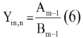
- n A m ⁇ 1 B m ⁇ 1
- a m-1 b m-1 A m-2 +a m-1 A m-3
- B m-1 b m-1 B m-2 +a m-1 B m-3 .
- P 1 Z 0 6
- P 2 ⁇ R 2 Z 0 4 ⁇ Z 0 4 X max X min + Z 0 4 X max 2 + Z 0 4 X min 2
- P 3 R 4 Z 0 2 ⁇ 6
- P 4 R 6 ⁇ R 4 X min X max ⁇ R 2 X min 3 X max + R 2 X max 2 X min 2 ⁇ R 2 X min X max 3 + R 4 X max 2 + R 4 X min 2 ⁇ X max 3 X min 3
- the first four roots of (13) are always complex conjugate, while the remaining two roots are real with equal magnitude, but opposite signs. As such, there is always one solution to (13) that yields the optimum value of the parameter q .
- the first term on the right represents the insertion loss of the reflective circuit of the proposed phase shifter.
- the second term on the right is the insertion loss of a 3-dB coupler.
- (11) and (16) demonstrate the potential of the proposed circuit - to increase the amount of phase shift of the phase shifter in a linear fashion with respect to the pairs of active elements, without increasing the insertion loss in the same linear fashion.
- the insertion loss of a 3-dB coupler is 0.3 dB (2*0.3 dB in the phase shifter configuration)
- q 1
- the active elements are capacitors formed using EC material as will be described next below.
- Figure 6 shows a parallel plate capacitor 10 in cross-section.
- ground plate 12 On which lies a first electrochromic layer 14 and a second electrochromic layer 18 separated by an electrolyte layer (in other words a dielectric layer) 16.
- an electrolyte layer in other words a dielectric layer
- top electrode 20 On top of the second electrochromic layer is a top electrode 20. It may be considered that the ground plate (also known as the ground electrode) 12 and the top electrode 20 effectively "sandwich" the intermediate active layers 14, 16,18.
- An electrochromic material is a material the optical absorption/transmission characteristics of which can be reversibly changed by the application of an external voltage, light source, or electric field.
- Examples include (i) transition-metal and inorganic oxides such as tungsten oxide, (ii) small organic molecules such as viologens, and (iii) polymers such a poly-viologens and derivatives of polythiophence, polypyrrole and polyaniline.
- the first EC layer 14 comprises a suitable EC material, such as WO 3 in this example.
- the EC material is TiO 2 , MoO 3 , Ta 2 O 5 , Nb 2 O 5 , or another of the above -mentioned electrochromic materials.
- the second EC layer 18 comprises NiO in this example.
- this layer is Cr 2 O 3 , MnO 2 , FeO 2 , CoO 2 , RhO 2 , IrO 2 , or another suitable material.
- the second EC layer 18 acts as an ion-storage layer.
- ground plate 12 is a cathode and the top electrode is an anode.
- the electrolyte layer 16 acts as an ion-conductor layer.
- the electrolyte layer 16 serves as a reservoir of ions for injection into the first EC layer 14.
- the electrolyte layer 16 also receives ions from the second EC layer 18.
- the phase shift provided by the phase shifter is at least substantially proportional to N where N is the number of reflective loads, in other words the number of capacitors.
- FIG. 7 A notional phase shifter 30 of nth order is shown in Figure 7 which is in accordance with the circuit shown in Figure 4 .
- the capacitors 10 are embedded in the substrate such that, each capacitor 10 has its respective top electrode 20 flush with (in other words in the same plane as) the top surface of the supporting substrate 28 so that the microstrip lines 26 can run flat.
- the microstrip line 26 has portions of different selected widths, hence different cross-sectional areas, to provide the respective impedance transformers.
- a 3-dB coupler 32 is a radio frequency (RF) device which splits an input RF signal into two signals equal in magnitude, but with a 90° phase shift between them for transmission to the capacitors 10.
- the 3dB-coupler has two input/output ports 34 and two other ports 36 for connection to the capacitors 10.
- the 3-dB coupler is replaced by a circulator (not shown).
- a circulator has three ports (one port less than the 3-dB coupler). Two ports of the circulator are input/output ports, whereas the last, third port is the port to which two or more reflective loads are connected.
- Each reflective load comprises a variable capacitor comprising EC materials as described with respect to Figure 6 , connected by at least two impedance transformers as described above made up of portions of microstrip line of different widths.
- Figure 8 shows a phase shifter where its circuit is as shown in Figures 4 and 7 with n selected as three. In other words, Figure 8 shows the 3 rd order reflective type phase shifter.
- Figure 9 shows a phase shifter where its circuit is as shown in Figures 4 and 7 with n selected as two. In other words, Figure 9 shows the 2nd order reflective type phase shifter.
- the proposed reflective type EC material based phase shifters of order two or more offer the benefits of lower loss and increased phase shift compared to an earlier approach. This can be seen, for example, in comparing the "second order" data, namely second and fourth rows of data in Table 1. This can also be seen, for example by comparing the "third order” data, namely the third and fifth row of data in Table 1.
- the capacitance ratio between the "ON” and “OFF” state can be tailored by the appropriate choice of the electrolyte, for which we have in-house experience.
- varactor diodes exhibit significant non-linear behaviour, whereas EC based materials are highly linear.
- program storage devices e.g., digital data storage media, which are machine or computer readable and encode machine-executable or computer-executable programs of instructions, wherein said instructions perform some or all of the steps of said above-described methods.
- the program storage devices may be, e.g., digital memories, magnetic storage media such as a magnetic disks and magnetic tapes, hard drives, or optically readable digital data storage media.
- Some embodiments involve computers programmed to perform said steps of the above-described methods.
Landscapes
- Waveguide Switches, Polarizers, And Phase Shifters (AREA)
Abstract

Description
- The present invention relates to a Radio Frequency reflection type phase shifter, and a method of Radio Frequency reflection type phase shifting.
- The reader is referred to the appended independent claims. Some preferred features are laid out in the dependent claims.
- An example of the present invention is a Radio Frequency reflection type phase shifter, the phase shifter comprising a coupler for input and output, and N variable capacitors, where N is an integer value of 2 or more, each of the variable capacitors providing radio frequency reflection, each of the variable capacitors being connected to the coupler by at least one of the impedance transformers, the characteristic impedances of the impedance transformers having been selected so that the phase shifter provides a phase shift at least substantially proportional to the value of N, wherein each of the variable capacitors comprises electrochromic material.
- The inventors realised that on the one hand capacitors using electrochromic materials were possible, for example as described in United States Patent Publication
US2015/00325897A1 - The inventors realised on the other hand a circuit as described in European Patent Publication
EP2996190 A1 was available using capacitors in the form of varactor diodes. - The inventors realised that the circuit described in
EP2996190A1 could be adapted to instead use capacitors using electrochromic materials as described inUS2015/00325897A1 - As compared to the prior approach described in
EP2996190A1 , four advantages of using EC based material as opposed to varactor diodes as active elements in the configuration of the proposed phase shifters are: (a) The exact values of the "ON" and "OFF" capacitance of EC based materials can be tailored by the surface area of the electrode end pads (this is not possible with varactor diodes); (b) The capacitance ratio between the "ON" and "OFF" state can be tailored by the appropriate choice of the electrolyte, for which we have in-house experience; (c) Varactor diodes exhibit a significant non-linear behaviour, whereas EC based materials are highly linear; (d) A possibility exists to actuate EC based materials by light, whereas this is not possible with varactor diodes. - Preferably each of the variable capacitors comprises an electrolyte element and at least one electrochromic element between a first electrode and a second electrode.
- Preferably, the first electrode comprises a ground plate on which lies the first electrochromic element, and the electrolyte element lies on the electrochromic element, the electrochromic element comprising an electrochromic layer, and the electrolyte element comprising an electrolyte layer.
- Preferably each of the variable capacitors further comprises a second electrochromic element between the electrolyte element and second electrode, the second electrochromic element comprising a second electrochromic layer.
- Preferably the coupler is a 3dB-coupler having four ports, N'/2 of the variable capacitors being connected to the coupler via one of two of the ports, and N'/2 of the capacitors being connected to the coupler via a second of said two ports, where N' is an even number integer of 4 or more. Alternatively preferably the coupler is a circulator having three ports, the N variable capacitors being connected to the circulator via one of the ports.
- Preferably the impedance transformers are microstrip lines.
- Preferably the characteristic impedances of the impedance transformers are selected in according with a selected value of a parameter value q determined for a given capacitor as

- Preferably the capacitance of each of the variable capacitors is variable by adjusting a d.c. voltage applied across the capacitors. Preferably said phase shift is at least substantially proportional to the value of N when a mid-range value of the capacitance of the variable capacitors is selected so the corresponding reactance at an operating radio frequency is the characteristic impedance Z0. Preferably the capacitors are variable between a higher capacitance 'fully ON' state when the d.c. voltage is at a first level and a lower capacitance 'OFF' state when the d.c. voltage is at a second level.
- Some preferred embodiments provide, as compared to existing solutions using EC materials, greater amounts of phase shift for lower insertion losses. Some preferred embodiments are suitable for the microwave frequency range.
- Examples of the present invention also relate to corresponding methods.
- An example of the present invention relates to a method of Radio Frequency reflection type phase shifting, by: applying an input signal to a phase shifter comprising a coupler for input and output, and N variable capacitors, where N is an integer value of 2 or more, each of the variable capacitors providing radio frequency reflection, each of the variable capacitors being connected to the coupler by at least one impedance transformer, the characteristic impedances of the impedance transformers having been selected so that the phase shifter provides a phase shift at least substantially proportional to the value of N, wherein each of the variable capacitors comprises electrochromic material; and receiving an output signal from the coupler.
- Preferably the capacitance of each of the variable capacitors is variable by adjusting a d.c. voltage applied across the capacitors.
- Preferably said phase shift is at least substantially proportional to the value of N when a mid-range value of the capacitance of the variable capacitors is selected so the corresponding reactance at an operating radio frequency is the characteristic impedance Z0.
- Embodiments of the present invention will now be described by way of example and with reference to the drawings, in which:
-
Figure 1 is a diagram illustrating a known Radio Frequency (RF) reflective type phase shifter (PRIOR ART), -
Figure 2 is a diagram illustrating a phase shifter which is two of the phase shifters shown inFigure 1 cascaded (PRIOR ART), -
Figure 3 is a diagram illustrating phase shifter which is three of the phase shifters shown inFigure 1 cascaded (PRIOR ART), -
Figure 4 is a general circuit diagram illustrating a generalised circuit of an RF reflective type phase shifter according to a first embodiment of the invention, generalised in the sense it is n-th order where n is two or more, -
Figure 5 is a circuit diagram illustrating part of the reflective loads portion of the circuit shown inFigure 4 , -
Figure 6 is a cross sectional view of a parallel plate capacitor including electrochromic (EC) material, multiple of which are used in the phase shifter shown inFigures 4 , -
Figure 7 is a perspective view of the generalised n-th order reflection type phase shifter shown inFigure 4 , -
Figure 8 is a diagram illustrates the phase shifter shown inFigures 4 and7 with n selected to be three, and -
Figure 9 is a diagram illustrating the phase shifter shown inFigures 4 and7 with n selected to be two. - We will first briefly outline the inventor's understanding of some earlier known approaches then focus in detail on embodiments of the present invention.
- A high frequency phase shifter based on EC materials is known from US Patent Publication
US 2015/0325897A1 . This high frequency phase shifter is based on the use of Electochromic (EC) material as bulk, dc induced tunable media in a circuit. - The inventors realised that this known high frequency EC material based phase shifter did not exploit the potential of EC materials. In particular, the circuit in that phase shifter only allowed modest values of phase shifts, typically up to 15 -30 degrees at frequencies around 3 GHz. In any particular case, the exact value of the phase shift obtained is, of course, dependent on the frequency of operation and the type and thickness of the EC material used, however, there is always a limitation as to how much phase shift can be obtained. Accordingly, the inventors saw a need for new architectures for high frequency phase shifters based on EC materials.
- This known approach of
US 2015/0325897A1 is illustrated inFigure 1 . As shown inFigure 1 , there is a ground plate on which an electrochromic layer is provided, and input and outputs connected via a 3dB coupler to microstrip contacts contacting the top of the EC layer. - The inventors realised that a problem with the phase shifter configuration of
Figure 1 lies in its inherently low values of achievable phase shifts. - The inventors realised that the amount of phase shift from the proposed configuration could be increased by cascading several structures of
Figure 1 as shown inFigures 2 and3 , but such an arrangements has drawbacks of increased structural size and complexity, and increased losses. As regards increased losses, since the number of 3-dB couplers will be increased, so will its corresponding insertion loss. The increase of the number of 3-dB couplers is particularly detrimental, since the radio frequency signal in any 3-dB coupler travels twice through - first to reach the reflective loads and second, back to reach the input/output ports. A 3-dB coupler is a radio frequency (RF) device which splits an input RF signal into two signals equal in magnitude, but with a 90° phase shift between them. - From noting these drawbacks, the need for different architectures for high frequency phase shifters based on EC materials became evident to the inventors.
- We now turn to describing some preferred embodiments.
- Firstly, a generic circuit for a range of phase shifters will be described. Secondly, the active elements used in the generic circuit will described, namely capacitors using EC material. Thirdly, example reflective type phase shifters will described that are in accordance with the generic circuit.
- As will be seen, in the generic circuit of
Figures 4 and5 , parallel plate capacitors are used formed using Electrochromic material as shown inFigure 6 . - After this description, we will present some comparison data comparing some properties of embodiments to examples of known approaches.
- The input admittance of the circuit in one of the reflective loads of the proposed circuit of
Fig. 4 is represented as
- Where,

- Or, in general,

- Here, ki,j,i= 2...n, j = 1, 2 represent the impedance transformers, n represents the order of the absorptive filter and Y=Z-1 . It can be inferred from (2) - (3) that the input admittance, Yin, can be represented in the form of a generalized continued fraction

- Or equivalently,


- The input admittance of the n-th order absorptive transmission zero can now be represented as
- Solving (6), one obtains the n-th order admittance polynomial from which the expression for the n-th order polynomial expression for the transmission coefficient of the notch filter (with the 3-dB coupler included) can be derived

- Substituting (6) into (7) and converting the admittance parameters into their impedance counterparts, i.e.


- In order for (8) to offer phase shift increase commensurate with the number of active elements in the reflective loads, (8) needs to be represented in the following form

Figs. 4 and5 . More generally, (9) can be written as

- For q=1, the phase shift of the proposed structure of
Figs. 4 and5 is increased n-times. Nevertheless, simply setting q=1, does not necessarily result in the optimal phase shift. The optimal phase shift is found by finding the roots of

- Where


- The first four roots of (13) are always complex conjugate, while the remaining two roots are real with equal magnitude, but opposite signs. As such, there is always one solution to (13) that yields the optimum value of the parameter q. The expression given by (14) can be simplified if it can be assumed that the parasitic resistance of an active element (i.e. parallel plate capacitor including EC material) can be neglected. This is a valid assumption in most cases, since this resistance is typically of the order of 1- 2 ohms. By setting R=0 (14) the optimal value q becomes

- The insertion loss of the proposed phase shifter (log scale) is

- Here, the first term on the right represents the insertion loss of the reflective circuit of the proposed phase shifter. For q=1 the insertion loss of the proposed reflective load is n-times higher than the insertion loss of the first order reflective circuit, while if parameter q is set in accordance with (13), the insertion loss of the reflective loads is always lower than that achieved with q=1. The second term on the right is the insertion loss of a 3-dB coupler.
- For comparison, a known phase shifter having cascade connection of n first order circuits will yield the same phase shift as (11), however, its insertion loss will be

- In quantitative terms, the reduction in the overall insertion loss of the proposed circuit over the known phase shifter having cascade connection is

- In view of (17) and (18), (11) and (16) demonstrate the potential of the proposed circuit - to increase the amount of phase shift of the phase shifter in a linear fashion with respect to the pairs of active elements, without increasing the insertion loss in the same linear fashion. For example, if the insertion loss of a 3-dB coupler is 0.3 dB (2*0.3 dB in the phase shifter configuration), and for n=2, q=1 the reduction of the insertion loss using the proposed circuit over the conventional cascade connection is

- In the derivation of the above equations the condition stipulated in the previous section related to the retention of a minimum number of 3-dB couplers in the design of the phase shifter has been fulfilled.
- The active elements are capacitors formed using EC material as will be described next below.
-
Figure 6 shows aparallel plate capacitor 10 in cross-section. - As shown in
Figure 6 , there is aground plate 12 on which lies afirst electrochromic layer 14 and asecond electrochromic layer 18 separated by an electrolyte layer (in other words a dielectric layer) 16. On top of the second electrochromic layer is atop electrode 20. It may be considered that the ground plate (also known as the ground electrode) 12 and thetop electrode 20 effectively "sandwich" the intermediateactive layers - An electrochromic material is a material the optical absorption/transmission characteristics of which can be reversibly changed by the application of an external voltage, light source, or electric field. Examples include (i) transition-metal and inorganic oxides such as tungsten oxide, (ii) small organic molecules such as viologens, and (iii) polymers such a poly-viologens and derivatives of polythiophence, polypyrrole and polyaniline.
- The
first EC layer 14 comprises a suitable EC material, such as WO3 in this example. In other examples, the EC material is TiO2, MoO3, Ta2O5, Nb2O5, or another of the above -mentioned electrochromic materials. - The
second EC layer 18 comprises NiO in this example. In other examples this layer is Cr2O3, MnO2, FeO2, CoO2, RhO2, IrO2, or another suitable material. In this example, thesecond EC layer 18 acts as an ion-storage layer. - In operation, the application of a d.c. bias voltage between the
ground plate 12 andtop electrode 20 induces changes in the dielectric characteristics of theintermediate layers ground plate 12 is a cathode and the top electrode is an anode. - The
electrolyte layer 16 acts as an ion-conductor layer. Theelectrolyte layer 16 serves as a reservoir of ions for injection into thefirst EC layer 14. In this example, theelectrolyte layer 16 also receives ions from thesecond EC layer 18. - When voltage is applied via
electrical leads ground electrode 12 andtop electrode 20. This electric field causes ions to be introduced into thefirst EC layer 14 fromelectrolyte layer 16. The electric charge caused by this injection of ions into thefirst EC layer 14 is neutralised by a corresponding charge balancing counter-flow of electrons fromground electrode 12. - In use the voltage is adjustable to vary the capacitance of the
capacitor 10 and is set to provide a capacitance corresponding to an impedance of characteristic impedance Z0, where Z0 is the characteristic impedance of theFigure 4 circuit. More specifically, the mid-range capacitance Cmid of thecapacitor 10 is selected (where Cmid = 0.5*(Cmax + Cmin) so that the reactance of the capacitor, which is a function of radio frequency and capacitance, matches the characteristic impedance Z0 of theFigure 4 circuit. In other word, the mid-range capacitance Cmid of thecapacitor 10 is selected so that Zmid = Z0 where Zmid=1/(ωCmid). - With the EC capacitors set to have this capacitance, the phase shift provided by the phase shifter is at least substantially proportional to N where N is the number of reflective loads, in other words the number of capacitors.
- A
notional phase shifter 30 of nth order is shown inFigure 7 which is in accordance with the circuit shown inFigure 4 . - As now shown in
Figure 7 , and as previously mentioned in relation toFigure 4 , ki,j,i = 2...n, j =1,2 represent the impedance transformers, and n represents the order of the phase shifter which may be considered an absorptive filter. - As shown in
Figure 7 , the impedance transformers ki,j, i = 2...n, j =1,2 are formed by microstrip lines 26 over a supportingsubstrate 28. Thecapacitors 10 are embedded in the substrate such that, eachcapacitor 10 has its respectivetop electrode 20 flush with (in other words in the same plane as) the top surface of the supportingsubstrate 28 so that the microstrip lines 26 can run flat. The microstrip line 26 has portions of different selected widths, hence different cross-sectional areas, to provide the respective impedance transformers. - As previously mentioned, as now shown in
Figure 7 , a 3-dB coupler 32 is a radio frequency (RF) device which splits an input RF signal into two signals equal in magnitude, but with a 90° phase shift between them for transmission to thecapacitors 10. The 3dB-coupler has two input/output ports 34 and twoother ports 36 for connection to thecapacitors 10. - In some otherwise similar embodiments (not shown), the 3-dB coupler is replaced by a circulator (not shown). A circulator has three ports (one port less than the 3-dB coupler). Two ports of the circulator are input/output ports, whereas the last, third port is the port to which two or more reflective loads are connected. Each reflective load comprises a variable capacitor comprising EC materials as described with respect to
Figure 6 , connected by at least two impedance transformers as described above made up of portions of microstrip line of different widths. -
Figure 8 shows a phase shifter where its circuit is as shown inFigures 4 and7 with n selected as three. In other words,Figure 8 shows the 3rd order reflective type phase shifter. - In one example, let us assume that the capacitance ratio between the "ON" and "OFF" state of the EC material based
capacitors 10 is 2 (Cmax/Cmin = 2) and that Cmin = 0.4 pF and that the EC material formedcapacitors 10 have an equivalent parasitic resistance of 1 ohm. - Setting n = 3 in (5) and substituting (5) into (8), the following expression for the transmission coefficient is obtained


- The condition that the discriminant of (21) is zero yields a triple zero at

- Solving (22) one obtains a quart-quadratic equation in


- The relationship between k22 and the rest of impedance transformers is found from (29). Imposing that the triple zero of (20) occurs at q · Z0, where q is a parameter that dictates the position of the transmission zero on the resistance scale, one obtains the following relationship for k22

- Substituting (28) into (27), the expression for


- The following conditions for the characteristic impedances, k12, k11 and k22 can now be expressed as

-
Figure 9 shows a phase shifter where its circuit is as shown inFigures 4 and7 with n selected as two. In other words,Figure 9 shows the 2nd order reflective type phase shifter. - In one example, let us assume that the capacitance ratio between the "ON" and "OFF" state of the EC material based
capacitors 10 is 2 (Cmax/Cmin = 2) and that Cmin = 0.4 pF and that the EC material formedcapacitors 10 have an equivalent parasitic resistance of 1 ohm. - Setting n = 2 in (5) and substituting (5) into (8), the following expression for the transmission coefficient is obtained

- (30) assumes that the 3-dB coupler is ideal. The zeroes of (30) yield the following values for the transformers k11 and k12
- Upon which (32) becomes

- By setting q=1 it follows

- For this comparison, with prior art approaches involving capacitors using EC materials, it is assumed that the capacitance ratio between the "ON" and "OFF" state of the EC material based
capacitors 10 is 2 (Cmax/Cmin = 2) and that Cmin = 0.4 pF and that the EC material formedcapacitors 10 have an equivalent parasitic resistance of 1 ohm. - Based on the information on the variable EC material based variable capacitors, the two phase shifters (one second order and one third order) shown in
Figures 8 and 9 were compared against prior art phase shifters involving capacitors using EC materials. In the design of all these phase shifters, a 3-dB coupler with an insertion loss of 0.3 dB is used. This is a realistic assumption and is evidenced in many practical designs. All three phase shifters are designed to operate at a centre frequency of 2. 5 GHz. Their performance is summarized in table 1 below.Table 1 Performance comparison of first, second and third order reflective type phase shifters Type of Phase Shifter Insertion phase (deg.) Insertion loss (dB) First order reflective type EC material based phase shifter ( Fig. 1 PRIOR ART)29.4 0.7 Second order reflective type EC material based phase shifter ( Fig. 9 )58.6 0.8 Third order reflective type EC material based phase shifter ( Fig. 8 )88.9 0.9 Second order reflective type EC material based phase shifter obtained by cascade connection of two first order phase shifters ( Fig. 2 PRIOR ART)58.8 1.4 Third order reflective type EC material based phase shifter obtained by cascade connection of three first order phase shifters( Fig. 3 PRIOR ART )88.2 2.1 - As shown in this table the proposed reflective type EC material based phase shifters of order two or more (n=2,3,4..) offer the benefits of lower loss and increased phase shift compared to an earlier approach. This can be seen, for example, in comparing the "second order" data, namely second and fourth rows of data in Table 1. This can also be seen, for example by comparing the "third order" data, namely the third and fifth row of data in Table 1.
- As compared to the prior approach described in
EP2996190A1 , some advantages of using EC based material as opposed to varactor diodes as the active elements in the configuration of the proposed phase shifters are as follows. - First, the exact values of the "ON" and "OFF" capacitance of EC based materials can be tailored by the surface area of the top electrodes- this is not possible with varactor diodes.
- Secondly, the capacitance ratio between the "ON" and "OFF" state can be tailored by the appropriate choice of the electrolyte, for which we have in-house experience.
- Thirdly, varactor diodes exhibit significant non-linear behaviour, whereas EC based materials are highly linear.
- Fourthly, a possibility exists in some other embodiments to actuate EC based materials by light, whereas this is not possible with varactor diodes.
- The present invention may be embodied in other specific forms without departing from its essential characteristics. The described embodiments are to be considered in all respects only as illustrative and not restrictive. The scope of the invention is, therefore, indicated by the appended claims rather than by the foregoing description. All changes that come within the meaning and range of equivalency of the claims are to be embraced within their scope.
- A person skilled in the art would readily recognize that steps of various above-described methods can be performed by programmed computers. Some embodiments relate to program storage devices, e.g., digital data storage media, which are machine or computer readable and encode machine-executable or computer-executable programs of instructions, wherein said instructions perform some or all of the steps of said above-described methods. The program storage devices may be, e.g., digital memories, magnetic storage media such as a magnetic disks and magnetic tapes, hard drives, or optically readable digital data storage media. Some embodiments involve computers programmed to perform said steps of the above-described methods.
Claims (13)
- A Radio Frequency reflection type phase shifter,the phase shifter comprising a coupler for input and output, and N variable capacitors, where N is an integer value of 2 or more, each of the variable capacitors providing in use radio frequency reflection,each of the variable capacitors being connected to the coupler by at least one impedance transformer, the characteristic impedances of the impedance transformers having been selected so that the phase shifter provides a phase shift at least substantially proportional to the value of N, wherein each of the variable capacitors comprises electrochromic material.
- A Radio Frequency reflection type phase shifter according to claim 1, in which each of the variable capacitors comprises an electrolyte element and at least one electrochromic element between a first electrode and a second electrode.
- A Radio Frequency reflection type phase shifter according to claim 2, in which the first electrode comprises a ground plate on which lies the first electrochromic element, and the electrolyte element lies on the electrochromic element, the electrochromic element comprising an electrochromic layer, and the electrolyte element comprising an electrolyte layer.
A Radio Frequency reflection type phase shifter according to claim 2 or claim 3, in which each of the variable capacitors further comprises a second electrochromic element between the electrolyte element and second electrode, the second electrochromic element comprising a second electrochromic layer. - A Radio Frequency reflection type phase shifter according to any preceding claim, in which the coupler is a 3dB-coupler having four ports, N'/2 of the variable capacitors being connected to the coupler via one of two of the ports, and N'/2 of the capacitors being connected to the coupler via a second of said two ports, where N' is an even number integer of 4 or more.
- A Radio Frequency reflection type phase shifter according to any of claims 1 to 4, in which the coupler is a circulator having three ports, the N variable capacitors being connected to the circulator via one of the ports.
- A Radio Frequency reflection type phase shifter according to any preceding claim, in which the impedance transformers are microstrip lines.
- A Radio Frequency reflection type phase shifter according to any preceding claim, in which the characteristic impedances of the impedance transformers are selected in accordance with a selected value of a parameter value q determined for a given capacitor as

- A Radio Frequency reflection type phase shifter according to any preceding claim, in which the capacitance of each of the variable capacitors is variable by adjusting a d.c. voltage applied across the capacitors.
- A Radio Frequency reflection type phase shifter according to claim 9, in which said phase shift is at least substantially proportional to the value of N when a mid-range value of the capacitance of the variable capacitors is selected so the corresponding reactance at an operating radio frequency is the characteristic impedance Z0.
- A Radio Frequency reflection type phase shifter according to claim 10, in which the capacitors are variable between a higher capacitance 'fully ON' state when the d.c. voltage is at a first level and a lower capacitance 'OFF' state when the d.c. voltage is at a second level.
- A method of Radio Frequency reflection type phase shifting, by:applying an input signal to a phase shifter comprising a coupler for input and output, and N variable capacitors, where N is an integer value of 2 or more, each of the variable capacitors providing radio frequency reflection, each of the variable capacitors being connected to the coupler by at least one impedance transformer, the characteristic impedances of the impedance transformers having been selected so that the phase shifter provides a phase shift at least substantially proportional to the value of N, wherein each of the variable capacitors comprises electrochromic material; andreceiving an output signal from the coupler.
- A method of Radio Frequency reflection type phase shifting according to claim 12, in which the capacitance of each of the variable capacitors is variable by adjusting a d.c. voltage applied across the capacitors.
- A method of Radio Frequency reflection type phase shifting according to claim 13, in which said phase shift is at least substantially proportional to the value of N when a mid-range value of the capacitance of the variable capacitors is selected so the corresponding reactance at an operating radio frequency is the characteristic impedance Z0.
Priority Applications (1)
| Application Number | Priority Date | Filing Date | Title |
|---|---|---|---|
| EP16306453.8A EP3319165B1 (en) | 2016-11-07 | 2016-11-07 | A radio frequency reflection type phase shifter, and method of phase shifting |
Applications Claiming Priority (1)
| Application Number | Priority Date | Filing Date | Title |
|---|---|---|---|
| EP16306453.8A EP3319165B1 (en) | 2016-11-07 | 2016-11-07 | A radio frequency reflection type phase shifter, and method of phase shifting |
Publications (2)
| Publication Number | Publication Date |
|---|---|
| EP3319165A1 true EP3319165A1 (en) | 2018-05-09 |
| EP3319165B1 EP3319165B1 (en) | 2020-03-18 |
Family
ID=57321248
Family Applications (1)
| Application Number | Title | Priority Date | Filing Date |
|---|---|---|---|
| EP16306453.8A Active EP3319165B1 (en) | 2016-11-07 | 2016-11-07 | A radio frequency reflection type phase shifter, and method of phase shifting |
Country Status (1)
| Country | Link |
|---|---|
| EP (1) | EP3319165B1 (en) |
Cited By (5)
| Publication number | Priority date | Publication date | Assignee | Title |
|---|---|---|---|---|
| CN110545085A (en) * | 2019-09-10 | 2019-12-06 | 大连海事大学 | A Frequency and Load Impedance Tunable Complex Impedance Converter |
| US11201634B2 (en) | 2020-03-27 | 2021-12-14 | Nokia Technologies Oy | Radio-frequency switching apparatus |
| CN113937440A (en) * | 2021-09-09 | 2022-01-14 | 电子科技大学长三角研究院(湖州) | Microstrip reflection type dynamic terahertz phase shifter based on varactor |
| CN114337723A (en) * | 2020-09-28 | 2022-04-12 | 诺基亚技术有限公司 | Radio communication |
| EP3989357A1 (en) * | 2020-10-22 | 2022-04-27 | Nokia Technologies Oy | Controllable radio frequency switching and/or splitting device |
Citations (6)
| Publication number | Priority date | Publication date | Assignee | Title |
|---|---|---|---|---|
| GB1186541A (en) * | 1966-02-25 | 1970-04-02 | American Cyanamid Co | Electro-Optical Devices |
| WO2000028613A1 (en) * | 1998-11-09 | 2000-05-18 | Paratek Microwave, Inc. | Ferroelectric varactor with built-in dc blocks |
| US6172385B1 (en) * | 1998-10-30 | 2001-01-09 | International Business Machines Corporation | Multilayer ferroelectric capacitor structure |
| EP1384286B1 (en) * | 2001-04-11 | 2006-06-14 | Kyocera Wireless Corp. | Inverted-f ferroelectric antenna |
| US20150325897A1 (en) | 2014-05-07 | 2015-11-12 | Alcatel-Lucent | Electrically controllable radio-frequency circuit element having an electrochromic material |
| EP2996190A1 (en) | 2014-09-09 | 2016-03-16 | Alcatel Lucent | Method for selecting a phase shift, phase shifter, beamformer and antenna array |
-
2016
- 2016-11-07 EP EP16306453.8A patent/EP3319165B1/en active Active
Patent Citations (6)
| Publication number | Priority date | Publication date | Assignee | Title |
|---|---|---|---|---|
| GB1186541A (en) * | 1966-02-25 | 1970-04-02 | American Cyanamid Co | Electro-Optical Devices |
| US6172385B1 (en) * | 1998-10-30 | 2001-01-09 | International Business Machines Corporation | Multilayer ferroelectric capacitor structure |
| WO2000028613A1 (en) * | 1998-11-09 | 2000-05-18 | Paratek Microwave, Inc. | Ferroelectric varactor with built-in dc blocks |
| EP1384286B1 (en) * | 2001-04-11 | 2006-06-14 | Kyocera Wireless Corp. | Inverted-f ferroelectric antenna |
| US20150325897A1 (en) | 2014-05-07 | 2015-11-12 | Alcatel-Lucent | Electrically controllable radio-frequency circuit element having an electrochromic material |
| EP2996190A1 (en) | 2014-09-09 | 2016-03-16 | Alcatel Lucent | Method for selecting a phase shift, phase shifter, beamformer and antenna array |
Non-Patent Citations (1)
| Title |
|---|
| SUBRAMANYAM G ET AL: "Thermally controlled vanadium dioxide thin film microwave devices", 2013 IEEE 56TH INTERNATIONAL MIDWEST SYMPOSIUM ON CIRCUITS AND SYSTEMS (MWSCAS), IEEE, 4 August 2013 (2013-08-04), pages 73 - 76, XP032525526, ISSN: 1548-3746, ISBN: 978-1-4799-4134-6, [retrieved on 20131124], DOI: 10.1109/MWSCAS.2013.6674588 * |
Cited By (8)
| Publication number | Priority date | Publication date | Assignee | Title |
|---|---|---|---|---|
| CN110545085A (en) * | 2019-09-10 | 2019-12-06 | 大连海事大学 | A Frequency and Load Impedance Tunable Complex Impedance Converter |
| CN110545085B (en) * | 2019-09-10 | 2023-02-10 | 大连海事大学 | A Complex Impedance Transformer with Tunable Frequency and Load Impedance |
| US11201634B2 (en) | 2020-03-27 | 2021-12-14 | Nokia Technologies Oy | Radio-frequency switching apparatus |
| CN114337723A (en) * | 2020-09-28 | 2022-04-12 | 诺基亚技术有限公司 | Radio communication |
| EP3989357A1 (en) * | 2020-10-22 | 2022-04-27 | Nokia Technologies Oy | Controllable radio frequency switching and/or splitting device |
| US11811124B2 (en) | 2020-10-22 | 2023-11-07 | Nokia Technologies Oy | Controllable radio frequency switching and/or splitting device |
| CN113937440A (en) * | 2021-09-09 | 2022-01-14 | 电子科技大学长三角研究院(湖州) | Microstrip reflection type dynamic terahertz phase shifter based on varactor |
| CN113937440B (en) * | 2021-09-09 | 2022-05-27 | 电子科技大学长三角研究院(湖州) | Microstrip reflection type dynamic terahertz phase shifter based on varactor |
Also Published As
| Publication number | Publication date |
|---|---|
| EP3319165B1 (en) | 2020-03-18 |
Similar Documents
| Publication | Publication Date | Title |
|---|---|---|
| US10804587B2 (en) | Electrically controllable radio-frequency circuit element having an electrochromic material | |
| EP3319165B1 (en) | A radio frequency reflection type phase shifter, and method of phase shifting | |
| KR100582548B1 (en) | Phase Shifter with PPU Structure Using Ferroelectric Thin Film | |
| US12206367B2 (en) | Traveling wave parametric amplifier | |
| EP3561890B1 (en) | Electrochromic switch | |
| US20140077894A1 (en) | Phase shifting device | |
| US10732476B2 (en) | Electrochromic cell | |
| CN109937510B (en) | Devices based on variable dielectric constant | |
| US20210075079A1 (en) | Electrically tunable radio-frequency components and circuits | |
| US20150325897A1 (en) | Electrically controllable radio-frequency circuit element having an electrochromic material | |
| US7031558B2 (en) | Low-pass filter transmission line with integral electroabsorption modulator | |
| US20260031517A1 (en) | Phase shifter and electronic device | |
| EP2544369B1 (en) | Attenuator | |
| US20050040915A1 (en) | Distributed analog phase shifter using etched ferroelectric thin film and method of manufacturing the same | |
| Shen et al. | Coupled‐line directional coupler with tunable power division ratio and operating frequency | |
| CN100442596C (en) | Phase shifter with aperiodic capacitive loading | |
| KR102521193B1 (en) | Apparatus and method for controlling a phase of a signal | |
| US11594795B2 (en) | Switchable element | |
| EP3893326A1 (en) | Apparatus comprising a waveguide for radio frequency signals | |
| Takeda et al. | Study of microstrip-based Terahertz phase shifter using liquid crystal | |
| US11556042B2 (en) | RF chirp reduction in MZ modulator | |
| US10594289B2 (en) | Apparatus and method for controlling phase of signal | |
| Subramanyam et al. | Ferroelectric thin-film based electrically tunable Ku-band coplanar waveguide components | |
| Chung et al. | Broadband phase shifters using complementary frequency‐dependent Δphase of low‐/high‐pass filters | |
| EP2996190A1 (en) | Method for selecting a phase shift, phase shifter, beamformer and antenna array |
Legal Events
| Date | Code | Title | Description |
|---|---|---|---|
| PUAI | Public reference made under article 153(3) epc to a published international application that has entered the european phase |
Free format text: ORIGINAL CODE: 0009012 |
|
| STAA | Information on the status of an ep patent application or granted ep patent |
Free format text: STATUS: THE APPLICATION HAS BEEN PUBLISHED |
|
| AK | Designated contracting states |
Kind code of ref document: A1 Designated state(s): AL AT BE BG CH CY CZ DE DK EE ES FI FR GB GR HR HU IE IS IT LI LT LU LV MC MK MT NL NO PL PT RO RS SE SI SK SM TR |
|
| AX | Request for extension of the european patent |
Extension state: BA ME |
|
| STAA | Information on the status of an ep patent application or granted ep patent |
Free format text: STATUS: REQUEST FOR EXAMINATION WAS MADE |
|
| 17P | Request for examination filed |
Effective date: 20181109 |
|
| RBV | Designated contracting states (corrected) |
Designated state(s): AL AT BE BG CH CY CZ DE DK EE ES FI FR GB GR HR HU IE IS IT LI LT LU LV MC MK MT NL NO PL PT RO RS SE SI SK SM TR |
|
| RAP1 | Party data changed (applicant data changed or rights of an application transferred) |
Owner name: NOKIA TECHNOLOGIES OY |
|
| GRAP | Despatch of communication of intention to grant a patent |
Free format text: ORIGINAL CODE: EPIDOSNIGR1 |
|
| STAA | Information on the status of an ep patent application or granted ep patent |
Free format text: STATUS: GRANT OF PATENT IS INTENDED |
|
| INTG | Intention to grant announced |
Effective date: 20191015 |
|
| GRAS | Grant fee paid |
Free format text: ORIGINAL CODE: EPIDOSNIGR3 |
|
| GRAA | (expected) grant |
Free format text: ORIGINAL CODE: 0009210 |
|
| STAA | Information on the status of an ep patent application or granted ep patent |
Free format text: STATUS: THE PATENT HAS BEEN GRANTED |
|
| AK | Designated contracting states |
Kind code of ref document: B1 Designated state(s): AL AT BE BG CH CY CZ DE DK EE ES FI FR GB GR HR HU IE IS IT LI LT LU LV MC MK MT NL NO PL PT RO RS SE SI SK SM TR |
|
| REG | Reference to a national code |
Ref country code: GB Ref legal event code: FG4D |
|
| REG | Reference to a national code |
Ref country code: DE Ref legal event code: R096 Ref document number: 602016031952 Country of ref document: DE |
|
| REG | Reference to a national code |
Ref country code: AT Ref legal event code: REF Ref document number: 1247001 Country of ref document: AT Kind code of ref document: T Effective date: 20200415 Ref country code: IE Ref legal event code: FG4D |
|
| PG25 | Lapsed in a contracting state [announced via postgrant information from national office to epo] |
Ref country code: RS Free format text: LAPSE BECAUSE OF FAILURE TO SUBMIT A TRANSLATION OF THE DESCRIPTION OR TO PAY THE FEE WITHIN THE PRESCRIBED TIME-LIMIT Effective date: 20200318 Ref country code: FI Free format text: LAPSE BECAUSE OF FAILURE TO SUBMIT A TRANSLATION OF THE DESCRIPTION OR TO PAY THE FEE WITHIN THE PRESCRIBED TIME-LIMIT Effective date: 20200318 Ref country code: NO Free format text: LAPSE BECAUSE OF FAILURE TO SUBMIT A TRANSLATION OF THE DESCRIPTION OR TO PAY THE FEE WITHIN THE PRESCRIBED TIME-LIMIT Effective date: 20200618 |
|
| REG | Reference to a national code |
Ref country code: NL Ref legal event code: MP Effective date: 20200318 |
|
| PG25 | Lapsed in a contracting state [announced via postgrant information from national office to epo] |
Ref country code: BG Free format text: LAPSE BECAUSE OF FAILURE TO SUBMIT A TRANSLATION OF THE DESCRIPTION OR TO PAY THE FEE WITHIN THE PRESCRIBED TIME-LIMIT Effective date: 20200618 Ref country code: GR Free format text: LAPSE BECAUSE OF FAILURE TO SUBMIT A TRANSLATION OF THE DESCRIPTION OR TO PAY THE FEE WITHIN THE PRESCRIBED TIME-LIMIT Effective date: 20200619 Ref country code: SE Free format text: LAPSE BECAUSE OF FAILURE TO SUBMIT A TRANSLATION OF THE DESCRIPTION OR TO PAY THE FEE WITHIN THE PRESCRIBED TIME-LIMIT Effective date: 20200318 Ref country code: LV Free format text: LAPSE BECAUSE OF FAILURE TO SUBMIT A TRANSLATION OF THE DESCRIPTION OR TO PAY THE FEE WITHIN THE PRESCRIBED TIME-LIMIT Effective date: 20200318 Ref country code: HR Free format text: LAPSE BECAUSE OF FAILURE TO SUBMIT A TRANSLATION OF THE DESCRIPTION OR TO PAY THE FEE WITHIN THE PRESCRIBED TIME-LIMIT Effective date: 20200318 |
|
| REG | Reference to a national code |
Ref country code: LT Ref legal event code: MG4D |
|
| PG25 | Lapsed in a contracting state [announced via postgrant information from national office to epo] |
Ref country code: NL Free format text: LAPSE BECAUSE OF FAILURE TO SUBMIT A TRANSLATION OF THE DESCRIPTION OR TO PAY THE FEE WITHIN THE PRESCRIBED TIME-LIMIT Effective date: 20200318 |
|
| PG25 | Lapsed in a contracting state [announced via postgrant information from national office to epo] |
Ref country code: SM Free format text: LAPSE BECAUSE OF FAILURE TO SUBMIT A TRANSLATION OF THE DESCRIPTION OR TO PAY THE FEE WITHIN THE PRESCRIBED TIME-LIMIT Effective date: 20200318 Ref country code: PT Free format text: LAPSE BECAUSE OF FAILURE TO SUBMIT A TRANSLATION OF THE DESCRIPTION OR TO PAY THE FEE WITHIN THE PRESCRIBED TIME-LIMIT Effective date: 20200812 Ref country code: EE Free format text: LAPSE BECAUSE OF FAILURE TO SUBMIT A TRANSLATION OF THE DESCRIPTION OR TO PAY THE FEE WITHIN THE PRESCRIBED TIME-LIMIT Effective date: 20200318 Ref country code: SK Free format text: LAPSE BECAUSE OF FAILURE TO SUBMIT A TRANSLATION OF THE DESCRIPTION OR TO PAY THE FEE WITHIN THE PRESCRIBED TIME-LIMIT Effective date: 20200318 Ref country code: IS Free format text: LAPSE BECAUSE OF FAILURE TO SUBMIT A TRANSLATION OF THE DESCRIPTION OR TO PAY THE FEE WITHIN THE PRESCRIBED TIME-LIMIT Effective date: 20200718 Ref country code: RO Free format text: LAPSE BECAUSE OF FAILURE TO SUBMIT A TRANSLATION OF THE DESCRIPTION OR TO PAY THE FEE WITHIN THE PRESCRIBED TIME-LIMIT Effective date: 20200318 Ref country code: LT Free format text: LAPSE BECAUSE OF FAILURE TO SUBMIT A TRANSLATION OF THE DESCRIPTION OR TO PAY THE FEE WITHIN THE PRESCRIBED TIME-LIMIT Effective date: 20200318 Ref country code: CZ Free format text: LAPSE BECAUSE OF FAILURE TO SUBMIT A TRANSLATION OF THE DESCRIPTION OR TO PAY THE FEE WITHIN THE PRESCRIBED TIME-LIMIT Effective date: 20200318 |
|
| REG | Reference to a national code |
Ref country code: AT Ref legal event code: MK05 Ref document number: 1247001 Country of ref document: AT Kind code of ref document: T Effective date: 20200318 |
|
| REG | Reference to a national code |
Ref country code: DE Ref legal event code: R097 Ref document number: 602016031952 Country of ref document: DE |
|
| PLBE | No opposition filed within time limit |
Free format text: ORIGINAL CODE: 0009261 |
|
| STAA | Information on the status of an ep patent application or granted ep patent |
Free format text: STATUS: NO OPPOSITION FILED WITHIN TIME LIMIT |
|
| PG25 | Lapsed in a contracting state [announced via postgrant information from national office to epo] |
Ref country code: IT Free format text: LAPSE BECAUSE OF FAILURE TO SUBMIT A TRANSLATION OF THE DESCRIPTION OR TO PAY THE FEE WITHIN THE PRESCRIBED TIME-LIMIT Effective date: 20200318 Ref country code: AT Free format text: LAPSE BECAUSE OF FAILURE TO SUBMIT A TRANSLATION OF THE DESCRIPTION OR TO PAY THE FEE WITHIN THE PRESCRIBED TIME-LIMIT Effective date: 20200318 Ref country code: DK Free format text: LAPSE BECAUSE OF FAILURE TO SUBMIT A TRANSLATION OF THE DESCRIPTION OR TO PAY THE FEE WITHIN THE PRESCRIBED TIME-LIMIT Effective date: 20200318 Ref country code: ES Free format text: LAPSE BECAUSE OF FAILURE TO SUBMIT A TRANSLATION OF THE DESCRIPTION OR TO PAY THE FEE WITHIN THE PRESCRIBED TIME-LIMIT Effective date: 20200318 |
|
| 26N | No opposition filed |
Effective date: 20201221 |
|
| PG25 | Lapsed in a contracting state [announced via postgrant information from national office to epo] |
Ref country code: PL Free format text: LAPSE BECAUSE OF FAILURE TO SUBMIT A TRANSLATION OF THE DESCRIPTION OR TO PAY THE FEE WITHIN THE PRESCRIBED TIME-LIMIT Effective date: 20200318 |
|
| PG25 | Lapsed in a contracting state [announced via postgrant information from national office to epo] |
Ref country code: SI Free format text: LAPSE BECAUSE OF FAILURE TO SUBMIT A TRANSLATION OF THE DESCRIPTION OR TO PAY THE FEE WITHIN THE PRESCRIBED TIME-LIMIT Effective date: 20200318 |
|
| PG25 | Lapsed in a contracting state [announced via postgrant information from national office to epo] |
Ref country code: MC Free format text: LAPSE BECAUSE OF FAILURE TO SUBMIT A TRANSLATION OF THE DESCRIPTION OR TO PAY THE FEE WITHIN THE PRESCRIBED TIME-LIMIT Effective date: 20200318 |
|
| REG | Reference to a national code |
Ref country code: CH Ref legal event code: PL |
|
| PG25 | Lapsed in a contracting state [announced via postgrant information from national office to epo] |
Ref country code: LU Free format text: LAPSE BECAUSE OF NON-PAYMENT OF DUE FEES Effective date: 20201107 |
|
| REG | Reference to a national code |
Ref country code: BE Ref legal event code: MM Effective date: 20201130 |
|
| PG25 | Lapsed in a contracting state [announced via postgrant information from national office to epo] |
Ref country code: LI Free format text: LAPSE BECAUSE OF NON-PAYMENT OF DUE FEES Effective date: 20201130 Ref country code: CH Free format text: LAPSE BECAUSE OF NON-PAYMENT OF DUE FEES Effective date: 20201130 |
|
| PG25 | Lapsed in a contracting state [announced via postgrant information from national office to epo] |
Ref country code: IE Free format text: LAPSE BECAUSE OF NON-PAYMENT OF DUE FEES Effective date: 20201107 |
|
| PG25 | Lapsed in a contracting state [announced via postgrant information from national office to epo] |
Ref country code: TR Free format text: LAPSE BECAUSE OF FAILURE TO SUBMIT A TRANSLATION OF THE DESCRIPTION OR TO PAY THE FEE WITHIN THE PRESCRIBED TIME-LIMIT Effective date: 20200318 Ref country code: MT Free format text: LAPSE BECAUSE OF FAILURE TO SUBMIT A TRANSLATION OF THE DESCRIPTION OR TO PAY THE FEE WITHIN THE PRESCRIBED TIME-LIMIT Effective date: 20200318 Ref country code: CY Free format text: LAPSE BECAUSE OF FAILURE TO SUBMIT A TRANSLATION OF THE DESCRIPTION OR TO PAY THE FEE WITHIN THE PRESCRIBED TIME-LIMIT Effective date: 20200318 |
|
| PG25 | Lapsed in a contracting state [announced via postgrant information from national office to epo] |
Ref country code: MK Free format text: LAPSE BECAUSE OF FAILURE TO SUBMIT A TRANSLATION OF THE DESCRIPTION OR TO PAY THE FEE WITHIN THE PRESCRIBED TIME-LIMIT Effective date: 20200318 Ref country code: AL Free format text: LAPSE BECAUSE OF FAILURE TO SUBMIT A TRANSLATION OF THE DESCRIPTION OR TO PAY THE FEE WITHIN THE PRESCRIBED TIME-LIMIT Effective date: 20200318 |
|
| PG25 | Lapsed in a contracting state [announced via postgrant information from national office to epo] |
Ref country code: BE Free format text: LAPSE BECAUSE OF NON-PAYMENT OF DUE FEES Effective date: 20201130 |
|
| PGFP | Annual fee paid to national office [announced via postgrant information from national office to epo] |
Ref country code: FR Payment date: 20250930 Year of fee payment: 10 |
|
| PGFP | Annual fee paid to national office [announced via postgrant information from national office to epo] |
Ref country code: DE Payment date: 20250930 Year of fee payment: 10 |
|
| PGFP | Annual fee paid to national office [announced via postgrant information from national office to epo] |
Ref country code: GB Payment date: 20251001 Year of fee payment: 10 |