EP3301780A1 - Low voltage bus system - Google Patents
Low voltage bus system Download PDFInfo
- Publication number
- EP3301780A1 EP3301780A1 EP17193063.9A EP17193063A EP3301780A1 EP 3301780 A1 EP3301780 A1 EP 3301780A1 EP 17193063 A EP17193063 A EP 17193063A EP 3301780 A1 EP3301780 A1 EP 3301780A1
- Authority
- EP
- European Patent Office
- Prior art keywords
- charging module
- conductive
- electrical contacts
- rail
- recited
- Prior art date
- Legal status (The legal status is an assumption and is not a legal conclusion. Google has not performed a legal analysis and makes no representation as to the accuracy of the status listed.)
- Withdrawn
Links
Images


Classifications
-
- H—ELECTRICITY
- H01—ELECTRIC ELEMENTS
- H01R—ELECTRICALLY-CONDUCTIVE CONNECTIONS; STRUCTURAL ASSOCIATIONS OF A PLURALITY OF MUTUALLY-INSULATED ELECTRICAL CONNECTING ELEMENTS; COUPLING DEVICES; CURRENT COLLECTORS
- H01R13/00—Details of coupling devices of the kinds covered by groups H01R12/70 or H01R24/00 - H01R33/00
- H01R13/62—Means for facilitating engagement or disengagement of coupling parts or for holding them in engagement
- H01R13/6205—Two-part coupling devices held in engagement by a magnet
-
- H—ELECTRICITY
- H01—ELECTRIC ELEMENTS
- H01R—ELECTRICALLY-CONDUCTIVE CONNECTIONS; STRUCTURAL ASSOCIATIONS OF A PLURALITY OF MUTUALLY-INSULATED ELECTRICAL CONNECTING ELEMENTS; COUPLING DEVICES; CURRENT COLLECTORS
- H01R13/00—Details of coupling devices of the kinds covered by groups H01R12/70 or H01R24/00 - H01R33/00
- H01R13/02—Contact members
-
- H—ELECTRICITY
- H01—ELECTRIC ELEMENTS
- H01R—ELECTRICALLY-CONDUCTIVE CONNECTIONS; STRUCTURAL ASSOCIATIONS OF A PLURALITY OF MUTUALLY-INSULATED ELECTRICAL CONNECTING ELEMENTS; COUPLING DEVICES; CURRENT COLLECTORS
- H01R24/00—Two-part coupling devices, or either of their cooperating parts, characterised by their overall structure
- H01R24/60—Contacts spaced along planar side wall transverse to longitudinal axis of engagement
- H01R24/62—Sliding engagements with one side only, e.g. modular jack coupling devices
-
- H—ELECTRICITY
- H01—ELECTRIC ELEMENTS
- H01R—ELECTRICALLY-CONDUCTIVE CONNECTIONS; STRUCTURAL ASSOCIATIONS OF A PLURALITY OF MUTUALLY-INSULATED ELECTRICAL CONNECTING ELEMENTS; COUPLING DEVICES; CURRENT COLLECTORS
- H01R24/00—Two-part coupling devices, or either of their cooperating parts, characterised by their overall structure
- H01R24/86—Parallel contacts arranged about a common axis
-
- H—ELECTRICITY
- H01—ELECTRIC ELEMENTS
- H01R—ELECTRICALLY-CONDUCTIVE CONNECTIONS; STRUCTURAL ASSOCIATIONS OF A PLURALITY OF MUTUALLY-INSULATED ELECTRICAL CONNECTING ELEMENTS; COUPLING DEVICES; CURRENT COLLECTORS
- H01R25/00—Coupling parts adapted for simultaneous co-operation with two or more identical counterparts, e.g. for distributing energy to two or more circuits
- H01R25/14—Rails or bus-bars constructed so that the counterparts can be connected thereto at any point along their length
- H01R25/142—Their counterparts
-
- H02J7/70—
-
- H—ELECTRICITY
- H01—ELECTRIC ELEMENTS
- H01R—ELECTRICALLY-CONDUCTIVE CONNECTIONS; STRUCTURAL ASSOCIATIONS OF A PLURALITY OF MUTUALLY-INSULATED ELECTRICAL CONNECTING ELEMENTS; COUPLING DEVICES; CURRENT COLLECTORS
- H01R2107/00—Four or more poles
-
- H—ELECTRICITY
- H01—ELECTRIC ELEMENTS
- H01R—ELECTRICALLY-CONDUCTIVE CONNECTIONS; STRUCTURAL ASSOCIATIONS OF A PLURALITY OF MUTUALLY-INSULATED ELECTRICAL CONNECTING ELEMENTS; COUPLING DEVICES; CURRENT COLLECTORS
- H01R25/00—Coupling parts adapted for simultaneous co-operation with two or more identical counterparts, e.g. for distributing energy to two or more circuits
- H01R25/14—Rails or bus-bars constructed so that the counterparts can be connected thereto at any point along their length
- H01R25/147—Low voltage devices, i.e. safe to touch live conductors
Definitions
- the following particularly describes a method for making a low voltage bus system whereby it will be ensured that the electrical contacts of a charging module will make and maintain continuous electrical connection with charging rails of a conductive bus regardless of the use orientation of the charging module relative to the conductive bus.
- the following is intended to provide a guideline for developing a charging module usable with a conductive bus having a center rail disposed intermediate a first conductive rail and a second conductive rail.
- the charging module has a base and the guidelines are usable to arrange a centered electrical contact and a first plurality of electrical contacts on the base.
- the centered electrical contact will be arranged on the base such that the centered electrical contact will engage with the center rail when the housing is placed into a use position on the conductive bus.
- the first plurality of electrical contacts will be arranged on the base along a perimeter of a first virtual circle that is generally centered on the centered electrical contact such that at least a first one of the first plurality of electrical contacts will engage with the first conductive rail and at least a second one of the first plurality of electrical contacts, different than the first one of the first plurality of electrical contacts, will engage with the second conductive rail when the housing is placed into the use position on the conductive bus in any rotational orientation of the housing relative to the conductive bus over a full 360 degrees.
- any one of the plurality of electrical contacts be capable of electrically coupling, or otherwise creating an electrical short condition between, the first conductive rail and the second conductive rail.
- the algorithms disclosed herein provide a means to design a charging module that will be able to be engaged with the conductive bus in any rotational orientation of the housing relative to the conductive bus over a full 360 degrees while using the minimal number of electrical contacts needed to achieve this purpose, the described system and method has the advantage of helping to reduce over system costs, e.g., it reduces the material costs associated with manufacturing a charging module, reduces the costs associated with purchasing and maintaining construction inventory, etc..
- the conductive bus system includes a charging module 100 that is intended to be electrically coupled to a conductive bus 200.
- the charging module 100 includes a plurality of electrical contacts 102 that are arranged such that a first circle 104 can be visualized to generally connect the plurality of electrical contacts 102 as shown in Figs. 1 and 4 .
- the charging module 100 may further include, or alternatively include, a plurality of electrical contacts 106 such that a second circle 108 can be visualized to generally connect the plurality of electrical contacts 106 as also shown in Fig. 1 .
- the plurality of electrical contacts 102 are intended to be used to provide a first direct voltage/current to the charging module 100 from the conductive bus 200 while the plurality of electrical contacts 106 are intended to be used to provide a second direct voltage/current to the charging module 100 from the conductive bus 200.
- the charging module 100 will further include electrical componentry for delivering a direct voltage/current received from the conductive bus 200 to a device that is coupled to the charging module 100.
- the charging module 100 may include, by way of example only, a universal serial bus (USB) port 110 for receiving a USB connector which, in turn, would be coupled to a device that is to be charged, such as a phone, computer, tablet, etc.
- the charging module 100 may yet further include an indicator 112, such as a light emitting diode (LED), to provide to a user an indication that the charging module 100 is receiving direct voltage/current from the conductive bus 200.
- LED light emitting diode
- the electrical contact 2 is in the form of a magnet.
- the electrical contact 2 is intended to, but need not be used to, receive a communication signal via the conductive bus 200.
- the communication signal received via the conductive bus 200 may be used to control functional operations of the charging module 100, e.g., to turn the charging module on/off, to throttle the amount of current that the charging module will draw from the conductive bus 200, etc.
- the communication signal received via the conductive bus 200 may additionally, or alternatively, be passed through the charging module 100 to the device that is coupled to the charging module 100 via the port 110 to thereby allow functional operations of the device being charged to be likewise controlled as desired.
- the conductive bus 200 to which the charging module 100 is to be coupled includes an elongated carrier 202 constructed from a non-conductive material.
- the carrier 202 includes a channel 203 in which is disposed a ferromagnetic rail 204.
- a surface 4 of the ferromagnetic rail 204 will preferably be exposed from the conductive bus 200 whereby the electrical contact 2 will be able to directly engage with the ferromagnetic rail 204 when the charging module 100 is disposed upon the conductive bus 200.
- the ferromagnetic rail 204 may be used to carry a communication signal, received from a controller that is coupled to the conductive bus 200, for provision to the charging module via the electrical contact 2 as described above.
- the carrier 202 further includes channels 205 and 206 for carrying conductive rails 207 and 208, respectively.
- a surface 3 of the conductive rails 207 and 208 will preferably be exposed from the conductive bus 200 whereby at least one of the plurality of electrical contacts 102 will be able to directly engage with the conductive rail 207 and at least one of the electrical contacts 102 will be able to directly engage with the conductive rail 208.
- the carrier 202 may further include, additionally or alternatively, channels 209 and 210 for carrying conductive rails 211 and 212, respectively.
- a surface 3 of the conductive rails 211 and 212 will preferably be exposed from the conductive bus 200 whereby at least one of the plurality of electrical contacts 106 will be able to directly engage with the conductive rail 211 and at least one of the electrical contacts 106 will be able to directly engage with the conductive rail 212.
- the carrier 202 illustrated in Fig. 2 is being provided by way of example only.
- the algorithms set forth hereinafter are to be used to determine the number of contacts 102 and/or 104 that are to be included in each set of the plurality of contacts, the positioning of the contacts 102 and/or 104 (as well as the contact 2), etc. given the design considerations of the conductive bus 200 and/or contacts available for use in constructing the charging module.
- the contact 2 be sized and arranged on the base of the charging module 100 such that, when the contact 2 is positioned in the vicinity of the rail 204, i.e., will be magnetically attracted thereto, the charging module 100 will generally center itself, i.e., generally center the virtual circles 102 and/or 106 upon a center line 204' of the rail 204, whereby, in any and all orientations of the charging module 100 relative to the conductive bus 204 at least one of the plurality of electrical contacts 102 will directly engage with the conductive rail 207 and at least one of the electrical contacts 102 will directly engage with the conductive rail 208 and, if used or in the alternative, at least one of the plurality of electrical contacts 106 will directly engage with the conductive rail 211 and at least one of the electrical contacts 106 will directly engage with the conductive rail 212.
- the algorithms described hereinafter function to optimize and output the orientation and number of contacts to be located on the base of the charging module 100 given the design considerations of the conductive bus 200 and the charging module 100, i.e., the aforementioned inputs.
- Table 1 and Table 2 set forth the various design inputs as well as the outputs to be generated where the generated outputs are to be employed to construct the charging module 100.
- the algorithms for generating these outputs then follow.
- the following nomenclature is applicable to the subject conductive bus system and the described methodology.
- Conductor rail - Strip (rail) of copper or other conductive material, e.g., rails 207, 208, 211, and 212, with a positive or negative charge, when the electrical contacts make contact with a positive and a negative conductor rail, power will flow to the charging module 100 ("CM").
- CM Electrical contact - conductive protrusion in the CM, e.g., contacts 102 and/or 106, that will come in contact with the conductor rail and allow power to flow to the CM, it is assumed to have a circular cross section but could be of a different shape without effecting design.
- Com contact - conductive protrusion in the CM e.g., contact 2
- the CM communications rail
- rail 204 e.g., rail 204
- Com rail - Strip (rail) of steel or other ferrous material, e.g., rail 204, that allows the CM to attach to the rail in a nonpermanent way, e.g., magnetically, and allow the rail to communicate to the CM.
- Perfect scenario - describes the case when all dimensions of actual product are true dimensions (tolerance is zero) and the center of the electrical contact circle is at the centerline of the com rail, e.g., 204', and the radius of the electrical contact circle, e.g., virtual circles 104 and/or 108, is tangent to the centerline of the conductor rail.
- Worst scenario - describes the case when the center of the electrical contact circle is moved laterally by the maximum allowable amount (Tp) from the centerline of the com rail and tolerances are at the maximum value.
- Root sum square - describes a mathematical formula where values are squared, summed together and the square root of that sum is taken, this provides an accurate measurement for multiple tolerances on a single object: n 1 2 + n 2 2 + n 3 2 + ⁇ + n i 2
- Housing - The part of the rail that holds the conductor and electrical rails in place, e.g., carrier 202, made of plastic or similar nonconductive material.
- CM Charging Module
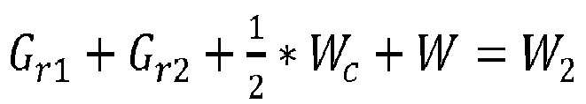
- G r is not constant between the com rail and inner conductor rail and the inner and outer conductor rails.
- G r + W + 1 2 ⁇ M d ⁇ 1 2 ⁇ 8 ⁇ T 5 ⁇ 1 2 ⁇ C dc ⁇ 1 2 ⁇ T 5 ⁇ G e ⁇ T 11 R o
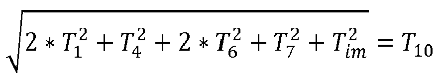
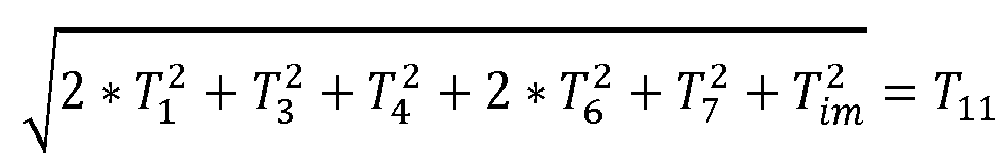
- T 1 2 + T 3 2 + T 4 2 + T 6 2 + T 7 2 + T im 2 T 11
- the algorithms set forth above provide a means to design a charging module that will be able to be engaged with the conductive bus in any rotational orientation of the housing relative to the conductive bus over a full 360 degrees while using the minimal number of electrical contacts needed to achieve this purpose.
- the described system and method has, among other advantages, the advantage of helping to reduce the material costs associated with manufacturing a charging module.
- the same (or very similar) electrical contacts will be used in the construction of the charging module, e.g., the electrical contacts for engaging with the conductive rails will all generally have the same rail surface engagement dimensions, the costs associated with purchasing and maintaining construction inventory will also be reduced.
Landscapes
- Charge And Discharge Circuits For Batteries Or The Like (AREA)
- Engineering & Computer Science (AREA)
- Power Engineering (AREA)
- Coupling Device And Connection With Printed Circuit (AREA)
Abstract
Description
- This application claims the benefit of U.S. Application No.
62/401,546, filed on September 29, 2016 -
U.S. Application No. 14/986,225 ,U.S. Application No. 14/857,918 ,U.S. Application No. 14/030,768 ,U.S. Provisional Application No. 61/725,795 U.S. Provisional Application No. 61/768,907 U.S. Provisional Application No. 61/744,777 U.S. Provisional Application No. 61/744,779 - The following particularly describes a method for making a low voltage bus system whereby it will be ensured that the electrical contacts of a charging module will make and maintain continuous electrical connection with charging rails of a conductive bus regardless of the use orientation of the charging module relative to the conductive bus. Specifically, the following is intended to provide a guideline for developing a charging module usable with a conductive bus having a center rail disposed intermediate a first conductive rail and a second conductive rail. The charging module has a base and the guidelines are usable to arrange a centered electrical contact and a first plurality of electrical contacts on the base. The centered electrical contact will be arranged on the base such that the centered electrical contact will engage with the center rail when the housing is placed into a use position on the conductive bus. The first plurality of electrical contacts will be arranged on the base along a perimeter of a first virtual circle that is generally centered on the centered electrical contact such that at least a first one of the first plurality of electrical contacts will engage with the first conductive rail and at least a second one of the first plurality of electrical contacts, different than the first one of the first plurality of electrical contacts, will engage with the second conductive rail when the housing is placed into the use position on the conductive bus in any rotational orientation of the housing relative to the conductive bus over a full 360 degrees. In this regard, it will be understood that in no use position over the full 360 degrees will any one of the plurality of electrical contacts be capable of electrically coupling, or otherwise creating an electrical short condition between, the first conductive rail and the second conductive rail. Furthermore, because the algorithms disclosed herein provide a means to design a charging module that will be able to be engaged with the conductive bus in any rotational orientation of the housing relative to the conductive bus over a full 360 degrees while using the minimal number of electrical contacts needed to achieve this purpose, the described system and method has the advantage of helping to reduce over system costs, e.g., it reduces the material costs associated with manufacturing a charging module, reduces the costs associated with purchasing and maintaining construction inventory, etc..
- A better understanding of the objects, advantages, features, properties and relationships of the described personal air sampler will be obtained from the following detailed description and accompanying drawing that set forth illustrative embodiments that are indicative of the various ways in which the principles expressed hereinafter may be employed.
- For a better understanding of the subject low voltage bus system, reference may be had to preferred embodiments shown in the following drawings in which:
-
Figure 1 is a schematic diagram illustrating an exemplary contact configuration for a charging module created via use of the methodology described hereinafter; -
Figure 2 illustrates an exemplary carrier of the conductive bus for use in connection with a charging module; and -
Figures 3 and 4 illustrate an exemplary charging module. - It is to be noted that elements in the figures are illustrated for simplicity and clarity and have not necessarily been drawn to scale. For example, the dimensions of some of the elements in the figures may be exaggerated relative to other elements to help to improve understanding of description which follows.
- With reference to the figures, an exemplary conductive bus system is now described. In general, the conductive bus system includes a
charging module 100 that is intended to be electrically coupled to aconductive bus 200. Thecharging module 100 includes a plurality ofelectrical contacts 102 that are arranged such that afirst circle 104 can be visualized to generally connect the plurality ofelectrical contacts 102 as shown inFigs. 1 and4 . Thecharging module 100 may further include, or alternatively include, a plurality ofelectrical contacts 106 such that asecond circle 108 can be visualized to generally connect the plurality ofelectrical contacts 106 as also shown inFig. 1 . In a preferred embodiment, the plurality ofelectrical contacts 102 are intended to be used to provide a first direct voltage/current to thecharging module 100 from theconductive bus 200 while the plurality ofelectrical contacts 106 are intended to be used to provide a second direct voltage/current to thecharging module 100 from theconductive bus 200. Thecharging module 100 will further include electrical componentry for delivering a direct voltage/current received from theconductive bus 200 to a device that is coupled to thecharging module 100. To this end, thecharging module 100 may include, by way of example only, a universal serial bus (USB)port 110 for receiving a USB connector which, in turn, would be coupled to a device that is to be charged, such as a phone, computer, tablet, etc. Thecharging module 100 may yet further include anindicator 112, such as a light emitting diode (LED), to provide to a user an indication that thecharging module 100 is receiving direct voltage/current from theconductive bus 200. - As further illustrated in
Figs. 1 and4 , centered within the plurality ofelectrical contacts 102, i.e., centered within the visualizedfirst circle 104, and/or centered within the plurality ofelectrical contacts 106, i.e., centered within the visualizedsecond circle 108, is a furtherelectrical contact 2. In a preferred embodiment, theelectrical contact 2 is in the form of a magnet. Theelectrical contact 2 is intended to, but need not be used to, receive a communication signal via theconductive bus 200. The communication signal received via theconductive bus 200 may be used to control functional operations of thecharging module 100, e.g., to turn the charging module on/off, to throttle the amount of current that the charging module will draw from theconductive bus 200, etc. The communication signal received via theconductive bus 200 may additionally, or alternatively, be passed through thecharging module 100 to the device that is coupled to thecharging module 100 via theport 110 to thereby allow functional operations of the device being charged to be likewise controlled as desired. - The
conductive bus 200 to which thecharging module 100 is to be coupled includes anelongated carrier 202 constructed from a non-conductive material. In a preferred embodiment, thecarrier 202 includes achannel 203 in which is disposed aferromagnetic rail 204. When disposed within thechannel 203, asurface 4 of theferromagnetic rail 204 will preferably be exposed from theconductive bus 200 whereby theelectrical contact 2 will be able to directly engage with theferromagnetic rail 204 when thecharging module 100 is disposed upon theconductive bus 200. While not required, theferromagnetic rail 204 may be used to carry a communication signal, received from a controller that is coupled to theconductive bus 200, for provision to the charging module via theelectrical contact 2 as described above. Thecarrier 202 further includeschannels conductive rails channels surface 3 of theconductive rails conductive bus 200 whereby at least one of the plurality ofelectrical contacts 102 will be able to directly engage with theconductive rail 207 and at least one of theelectrical contacts 102 will be able to directly engage with theconductive rail 208. Thecarrier 202 may further include, additionally or alternatively,channels conductive rails channels surface 3 of theconductive rails conductive bus 200 whereby at least one of the plurality ofelectrical contacts 106 will be able to directly engage with theconductive rail 211 and at least one of theelectrical contacts 106 will be able to directly engage with theconductive rail 212. It will be understood that different configuration for thecarrier 202 may be utilized as required and, as such, thecarrier 202 illustrated inFig. 2 is being provided by way of example only. - To ensure that the
charging module 100 will engage with theconductive bus 200 to thereby allow thecharging module 100 to be electrically coupled to the conductive rails regardless of the use orientation of thecharging module 100 when positioned upon theconductive bus 200, i.e., in any orientation of thecharging module 100 throughout the full 360 degrees of the visualizedcircles 104 and/or 108 when thecontact 2 is engaged with therail 204 as shown inFig. 1 , the algorithms set forth hereinafter are to be used to determine the number ofcontacts 102 and/or 104 that are to be included in each set of the plurality of contacts, the positioning of thecontacts 102 and/or 104 (as well as the contact 2), etc. given the design considerations of theconductive bus 200 and/or contacts available for use in constructing the charging module. As concerns thecontact 2, it is preferred that thecontact 2 be sized and arranged on the base of thecharging module 100 such that, when thecontact 2 is positioned in the vicinity of therail 204, i.e., will be magnetically attracted thereto, thecharging module 100 will generally center itself, i.e., generally center thevirtual circles 102 and/or 106 upon a center line 204' of therail 204, whereby, in any and all orientations of thecharging module 100 relative to theconductive bus 204 at least one of the plurality ofelectrical contacts 102 will directly engage with theconductive rail 207 and at least one of theelectrical contacts 102 will directly engage with theconductive rail 208 and, if used or in the alternative, at least one of the plurality ofelectrical contacts 106 will directly engage with theconductive rail 211 and at least one of theelectrical contacts 106 will directly engage with theconductive rail 212. - More particularly and as described/illustrated further below, there are sixteen design inputs that may be changed to design the rail/charger interface depending on the shape of the charging module and/or the rail. Accordingly, the algorithms described hereinafter function to optimize and output the orientation and number of contacts to be located on the base of the
charging module 100 given the design considerations of theconductive bus 200 and thecharging module 100, i.e., the aforementioned inputs. - With reference to
Fig. 1 , Table 1 and Table 2 set forth the various design inputs as well as the outputs to be generated where the generated outputs are to be employed to construct thecharging module 100. The algorithms for generating these outputs then follow. In addition, the following nomenclature is applicable to the subject conductive bus system and the described methodology. - Conductor rail - Strip (rail) of copper or other conductive material, e.g.,
rails - Electrical contact - conductive protrusion in the CM, e.g.,
contacts 102 and/or 106, that will come in contact with the conductor rail and allow power to flow to the CM, it is assumed to have a circular cross section but could be of a different shape without effecting design. - Com contact - conductive protrusion in the CM, e.g.,
contact 2, that will come in contact with the com (communications) rail, e.g.,rail 204, and allow the CM (and, in some instances, a device being charged) to communicate with the rail software, it is assumed to have a circular cross section but could be of a different shape without effecting design. - Com rail - Strip (rail) of steel or other ferrous material, e.g.,
rail 204, that allows the CM to attach to the rail in a nonpermanent way, e.g., magnetically, and allow the rail to communicate to the CM. - Tolerance - A distance that describes the extreme low and high of actual dimensions compared to the true dimension, this is an allowable variation generally supplied from manufacturers.
- Perfect scenario - describes the case when all dimensions of actual product are true dimensions (tolerance is zero) and the center of the electrical contact circle is at the centerline of the com rail, e.g., 204', and the radius of the electrical contact circle, e.g.,
virtual circles 104 and/or 108, is tangent to the centerline of the conductor rail. - Worst scenario - describes the case when the center of the electrical contact circle is moved laterally by the maximum allowable amount (Tp) from the centerline of the com rail and tolerances are at the maximum value.
- Root sum square - describes a mathematical formula where values are squared, summed together and the square root of that sum is taken, this provides an accurate measurement for multiple tolerances on a single object:

- Housing - The part of the rail that holds the conductor and electrical rails in place, e.g.,
carrier 202, made of plastic or similar nonconductive material. - Charging Module (CM) - Device that houses the electrical contacts and the necessary electrical components to transmit power to an external device.
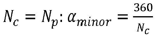
Table 1 Fig. 1 ElementVariable Equation Description Electrical Contact Inputs 1 Gr * Gap between exposed edges of conductor rails ** T1 * Tolerance on Gr (±) ** Cdm * Maximum outer diameter of electrical contact-this will limit how close the contacts can be in relation to each other ** T2 * Tolerance on Cdm (±) ** Cdc * Diameter of electrical contact that is in contact with the conductor rails ** T3 * Tolerance on Cdc (±) 2 Md * Communication (com) contact diameter ** T4 * Tolerance on Md (±) ** Tim * Tolerance of injection molding of Charging module (CM) base, which holds the electrical contacts Conductor and Com Rail Inputs 3 W * Exposed conductor rail width ** T6 * Tolerance on W (±) 4 Wc * Exposed com rail width ** T7 * Tolerance on Wc (±) ** Gc * Material gap between electrical contacts from inner edge to inner edge ** Ge * Minimum distance from outer edge of conductor rail to outer edge of contact ** T5 * Tolerance of flatness of conductor rail and housing (±) Table 2 Fig. 1 ElementVariable Equation Description 5 W 11 Distance from the center of the com rail to the inner edge of the conductor rail (Perfect scenario) 6 W 22 Distance from the center of the com rail to the outer edge of the conductor rail (Perfect scenario) 7 T p3 Distance the center of the CM can move from center of the com(±) ** R max4 Maximum electrical contact circle radius 8 R o5 Optimized electrical contact circle radius 9 α c6 Angle of individual electrical contact from edge to edge ** α cg7 Angle corresponding to Gc ** α min8 Minimum angle allowed between contacts from center to center ** R tp9 Center of contact circle to the outer edge of the conductor rail (Worst scenario) ** αmajor.int 10 Intermediate calculation of αmajor ** Nideal 11 Ideal number of electrical contacts Outputs ** Nc 12 Required number of electrical contacts ** N p13 Number of electrical circuit contacts ** α minor.int14 Intermediate calculation of αminor 12 αminor 15 Angle between contacts from center of sets 13 αmajor 16 Angle between sets of contacts from center to center 12 αminor2 17 Angle between contacts in a set when αminor is less than α min13 αmajor2 18 Angle between sets of contacts when αminor.int is less than αmin 14 Cd 19 Minimum electrical contact tip diameter of curvature to ensure contact with the conductor rail based on the flatness (T5) between the conductor rail and the housing ** T9 20 Root sum square of tolerances that effect Tp ** T10 21 Root sum square of tolerances that effect Rtp and Rmax ** T11 22 Root sum square of tolerances that effect Ro ** Mmax 23 Maximum magnet size ** Ncs 24 Number of electrical contacts per electrical circuit contact - Within the tables:
- * means these values are only inputs and, as such, there is no equation for them listed below in the algorithm section;
- ** means these values do not need pictorial representation or cannot be visually represented in a clear manner due to conditional factors; and
- *** means an arbitrary value input (see below)
- Thus, using the inputs noted above in tables 1 and 2, below are the algorithms for arriving at the spacing, etc. of the electrical contacts to ensure a constant electrical connection between the conductor rails and the electrical contacts in the
charging module 100. - Input - changed by user.
- Fixed values - from manufacturers or other internal sources which can vary from between manufacturers or processes.
- Intermediate calculations - these are values that are used to find the design requirements, but may not directly visible in the design of the CM.
- Design requirements - these calculations describe the optimal electrical contact layout based on the inputs and fixed values, some design outputs may not be used based on conditional outputs outlined below.

- For the inner conductor rail.
- a.

For the outer conductor rail if Gr is constant between the com rail and inner conductor rail and the inner and outer conductor rails. - b.

- For the outer conductor rail if Gr is not constant between the com rail and inner conductor rail and the inner and outer conductor rails.

- For the inner conductor rail.
- a.

For the outer conductor rail if Gr is constant between the com rail and inner conductor rail and the inner and outer conductor rails. - b.
- For the outer conductor rail if Gr is not constant between the com rail and inner conductor rail and the inner and outer conductor rails.


- For the inner conductor rail.
- a.

For the outer conductor rail if Gr is constant between the com rail and inner conductor rail and the inner and outer conductor rails. - b.

- For the outer conductor rail if Gr is not constant between the com rail and inner conductor rail and the inner and outer conductor rails.

- For the inner conductor rail.
- a.

For the outer conductor rail if Gr is constant between the com rail and inner conductor rail and the inner and outer conductor rails). - b.

- For the outer conductor rail, if Gr is not constant between the com rail and inner conductor rail and the inner and outer conductor rails.


- For the inner conductor rail.
- a.

For the outer conductor rail if Gr is constant between the com rail and inner conductor rail and the inner and outer conductor rails. - b.

- For the outer conductor rail if Gr is not constant between the com rail and inner conductor rail and the inner and outer conductor rails.


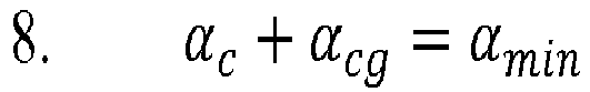
- a.

- This describes the upper and lower possibilities of Nc


- a.
- b. Nc ≠ Np :
- i. α aminor.int ≤ αmin : αminor = N/A
- ii. αminor.int ≥ αmin : αminor = αminor.int
- a. Nc = Np : αmajor = No Sets
- b. Nc ≠ Np :
- i. αminor.int < αmin : αmajor = N / A
- ii.

- a. Nc = Np : α minor2 No Sets
- b. Nc ≠ Np :
- i. αminor.int < αmin :α minor2 = αmin
- ii. αminor.int > αmin :α minor2 = N/A
- a. Nc = Np : αmajor = No Sets
- b. Nc ≠ Np :
- i.

- ii. αminor.int > αmin : α major2 = N/A
- i.
- For the inner conductor rail.
- a.
- For the outer conductor rail.

- For the inner conductor rail.
- a.
- For the outer conductor rail.


- As will now be appreciated, the algorithms set forth above provide a means to design a charging module that will be able to be engaged with the conductive bus in any rotational orientation of the housing relative to the conductive bus over a full 360 degrees while using the minimal number of electrical contacts needed to achieve this purpose. Thus, the described system and method has, among other advantages, the advantage of helping to reduce the material costs associated with manufacturing a charging module. Furthermore, because it is contemplated that the same (or very similar) electrical contacts will be used in the construction of the charging module, e.g., the electrical contacts for engaging with the conductive rails will all generally have the same rail surface engagement dimensions, the costs associated with purchasing and maintaining construction inventory will also be reduced.
- While specific embodiments of the invention have been described in detail, it will be appreciated by those skilled in the art that various modifications and alternatives to those details could be developed in light of the overall teachings of the disclosure. Accordingly, the particular arrangement disclosed is meant to be illustrative only and not limiting as to the scope of the invention which is to be given the full breadth of the appended claims and any equivalents thereof.
Claims (20)
- A charging module for use in connection with a conductive bus having non-conductive carrier which carries a center rail disposed intermediate a first conductive rail and a second conductive rail, the charging module comprising:a housing having a base on which is disposed a centered electrical contact and a first plurality of electrical contacts, wherein the centered electrical contact is arranged on the base such that the centered electrical contact will engage with the center rail when the housing is placed into a use position on the conductive bus, and the first plurality of electrical contacts are arranged on the base along a perimeter of a first virtual circle that is generally centered on the centered electrical contact such that at least a first one of the first plurality of electrical contacts will engage with the first conductive rail and at least a second one of the first plurality of electrical contacts, different than the first one of the first plurality of electrical contacts, will engage with the second conductive rail when the housing is placed into the use position on the conductive bus in any rotational orientation of the housing relative to the conductive bus over a full 360 degrees whereby power received from the conductive bus via an engagement between the first plurality of electrical contacts and the first conductive rail and/or the second conductive rail will be capable of being provided to a device coupled to the charging module.
- The charging module as recited in claim 1, wherein the non-conductive carrier carries a third conductive rail and a fourth conductive rail, a second plurality of electrical contacts are disposed on the base of the housing, the second plurality of electrical contacts are arranged on the base along a perimeter of a second virtual circle that is generally centered on the centered electrical contact such that at least a first one of the second plurality of electrical contacts will engage with the third conductive rail and at least a second one of the second plurality of electrical contacts, different than the first one of the second plurality of electrical contacts, will engage with the fourth conductive rail when the housing is placed into the use position on the conductive bus in any rotational orientation of the housing relative to the conductive bus over a full 360 degrees whereby power received from the conductive bus via an engagement between the second plurality of electrical contacts and the third conductive rail and/or the fourth conductive rail will be capable of being provided to a device coupled to the charging module.
- The charging module as recited in claim 1, wherein the first plurality of electrical contacts comprises at least five electrical contacts.
- The charging module as recited in claim 2, wherein the first plurality of electrical contacts comprises at least five electrical contacts and wherein the second plurality of electrical contacts comprises at least nine electrical contacts.
- The charging module as recited in claim 1, wherein the centered electrical contact is magnetically coupled to the center rail in the use position on the conductive bus.
- The charging module as recited in claim 5, wherein the housing will automatically place itself into the use position on the conductive bus when the centered electrical contact is freely positioned within a magnetically attractive distance from the center rail.
- The charging module as recited in claim 1, wherein the center rail carriers a communication signal and wherein the centered electrical contact is usable to receive the communication signal from the center rail for use by the charging module and/or the device coupled to the charging module when the housing is in the use position on the conductive bus.
- The charging module as recited in claim 1, wherein the housing has a port for use in electrically coupling the device to the charging module.
- The charging module as recited in claim 8, wherein the port comprises a universal serial bus port.
- The charging module as recited in claim 7, wherein the housing has a port for use in electrically and communicatively coupling the device to the charging module.
- The charging module as recited in claim 10, wherein the port comprises a universal serial bus port.
- The charging module as recited in claim 2, wherein the centered electrical contact is magnetically coupled to the center rail in the use position on the conductive bus.
- The charging module as recited in claim 12, wherein the housing will automatically place itself into the use position on the conductive bus when the centered electrical contact is freely positioned within a magnetically attractive distance from the center rail.
- The charging module as recited in claim 2, wherein the center rail carriers a communication signal and wherein the centered electrical contact is usable to receive the communication signal from the center rail for use by the charging module and/or the device coupled to the charging module when the housing is in the use position on the conductive bus.
- The charging module as recited in claim 2, wherein the housing has a port for use in electrically coupling the device to the charging module.
- The charging module as recited in claim 15, wherein the port comprises a universal serial bus port.
- The charging module as recited in claim 14, wherein the housing has a port for use in electrically and communicatively coupling the device to the charging module.
- The charging module as recited in claim 17, wherein the port comprises a universal serial bus port.
- The charging module as recited in claim 1, wherein the first plurality of electrical contacts each provide a similarly sized surface for engagement with the first and second conductive rails and the first plurality of electrical contacts has no more than a calculated minimal number of electrical contacts that is needed to allow the use position of the charging module to encompass any rotational orientation of the housing relative to the conductive bus over the full 360 degrees.
- The charging module as recited in claim 2, wherein the first plurality of electrical contacts each provide a similarly sized surface for engagement with the first and second conductive rails, the first plurality of electrical contacts has no more than a calculated minimal number of electrical contacts that is needed to allow the use position of the charging module to encompass any rotational orientation of the housing relative to the conductive bus over the full 360 degrees, the second plurality of electrical contacts each provide a similarly sized surface for engagement with the third and fourth conductive rails, and the second plurality of electrical contacts has no more than a calculated minimal number of electrical contacts that is needed to allow the use position of the charging module to encompass any rotational orientation of the housing relative to the conductive bus over the full 360 degrees.
Applications Claiming Priority (2)
| Application Number | Priority Date | Filing Date | Title |
|---|---|---|---|
| US201662401546P | 2016-09-29 | 2016-09-29 | |
| US15/701,145 US10218113B2 (en) | 2016-09-29 | 2017-09-11 | Low voltage bus system |
Publications (1)
| Publication Number | Publication Date |
|---|---|
| EP3301780A1 true EP3301780A1 (en) | 2018-04-04 |
Family
ID=60119785
Family Applications (1)
| Application Number | Title | Priority Date | Filing Date |
|---|---|---|---|
| EP17193063.9A Withdrawn EP3301780A1 (en) | 2016-09-29 | 2017-09-26 | Low voltage bus system |
Country Status (8)
| Country | Link |
|---|---|
| US (1) | US10218113B2 (en) |
| EP (1) | EP3301780A1 (en) |
| JP (1) | JP2018056127A (en) |
| CN (1) | CN107887727B (en) |
| AU (1) | AU2017235934A1 (en) |
| BR (1) | BR102017020852A2 (en) |
| MX (1) | MX2017012395A (en) |
| RU (1) | RU2017133516A (en) |
Cited By (1)
| Publication number | Priority date | Publication date | Assignee | Title |
|---|---|---|---|---|
| EP3618199A1 (en) * | 2018-08-28 | 2020-03-04 | Self Electronics Co., Ltd. | Shelf electrical supply system |
Families Citing this family (4)
| Publication number | Priority date | Publication date | Assignee | Title |
|---|---|---|---|---|
| USD833396S1 (en) * | 2017-04-21 | 2018-11-13 | Ideal Industries, Inc. | Electric buss rail carrier |
| USD833395S1 (en) * | 2017-04-21 | 2018-11-13 | Ideal Industries, Inc. | Electric buss rail carrier |
| USD833974S1 (en) * | 2017-04-21 | 2018-11-20 | Ideal Industries, Inc. | Electric buss rail carrier |
| USD832216S1 (en) * | 2017-04-21 | 2018-10-30 | Ideal Industries, Inc. | Electric buss rail carrier |
Citations (9)
| Publication number | Priority date | Publication date | Assignee | Title |
|---|---|---|---|---|
| FR2613883A1 (en) * | 1987-04-13 | 1988-10-14 | Scidepa Ste Civile Brevets | Device for supplying an electrical receiver placed on a surface including a network of lands (areas) made of electricity-conducting material |
| US6204632B1 (en) * | 1999-09-08 | 2001-03-20 | Selfcharge | Apparatus for charging multiple batteries |
| US20040048511A1 (en) * | 2002-03-01 | 2004-03-11 | Tal Dayan | Wirefree mobile device power supply method & system with free positioning |
| US20070194526A1 (en) * | 2002-12-10 | 2007-08-23 | Mitch Randall | System and method for providing power to an electronic device |
| WO2007099412A1 (en) * | 2006-02-28 | 2007-09-07 | Nokia Corporation | Providing an electrical circuit |
| FR2904894A1 (en) * | 2006-08-11 | 2008-02-15 | Tou Tong | Electrical supply device for e.g. telephone, has connection module comprising electrical contact elements placed in similar manner on two levels for permitting connection by respective physical contacts between elements and tracks |
| US20100022285A1 (en) * | 2008-03-03 | 2010-01-28 | Wildcharge, Inc. | Apparatus and method for retrofitting a broad range of mobile devices to receive wireless power |
| US20100055928A1 (en) * | 2008-07-24 | 2010-03-04 | Mitch Randall | Connector for providing power to a mobile electronic device |
| EP2582005A1 (en) * | 2011-10-14 | 2013-04-17 | Research In Motion Limited | Clip-on charging system with variable charging rates |
Family Cites Families (5)
| Publication number | Priority date | Publication date | Assignee | Title |
|---|---|---|---|---|
| US3521216A (en) * | 1968-06-19 | 1970-07-21 | Manuel Jerair Tolegian | Magnetic plug and socket assembly |
| CN202444150U (en) * | 2012-03-01 | 2012-09-19 | 刘祖光 | Combined type secure socket |
| US9678537B2 (en) * | 2013-04-30 | 2017-06-13 | Victor Kupferstein | Mobile device case and peripheral system |
| KR200489678Y1 (en) * | 2014-11-25 | 2019-07-23 | (주)에스피에스 | Thin film type magnetic connector module |
| AT516771B1 (en) * | 2015-01-30 | 2018-04-15 | Dipl Ing Bsc Flechl Christian | Plug connection and method for connecting in particular electrical lines |
-
2017
- 2017-09-11 US US15/701,145 patent/US10218113B2/en not_active Expired - Fee Related
- 2017-09-26 EP EP17193063.9A patent/EP3301780A1/en not_active Withdrawn
- 2017-09-27 MX MX2017012395A patent/MX2017012395A/en unknown
- 2017-09-27 AU AU2017235934A patent/AU2017235934A1/en not_active Abandoned
- 2017-09-27 RU RU2017133516A patent/RU2017133516A/en not_active Application Discontinuation
- 2017-09-28 CN CN201710897378.XA patent/CN107887727B/en not_active Expired - Fee Related
- 2017-09-28 BR BR102017020852-4A patent/BR102017020852A2/en not_active IP Right Cessation
- 2017-09-28 JP JP2017188449A patent/JP2018056127A/en not_active Withdrawn
Patent Citations (9)
| Publication number | Priority date | Publication date | Assignee | Title |
|---|---|---|---|---|
| FR2613883A1 (en) * | 1987-04-13 | 1988-10-14 | Scidepa Ste Civile Brevets | Device for supplying an electrical receiver placed on a surface including a network of lands (areas) made of electricity-conducting material |
| US6204632B1 (en) * | 1999-09-08 | 2001-03-20 | Selfcharge | Apparatus for charging multiple batteries |
| US20040048511A1 (en) * | 2002-03-01 | 2004-03-11 | Tal Dayan | Wirefree mobile device power supply method & system with free positioning |
| US20070194526A1 (en) * | 2002-12-10 | 2007-08-23 | Mitch Randall | System and method for providing power to an electronic device |
| WO2007099412A1 (en) * | 2006-02-28 | 2007-09-07 | Nokia Corporation | Providing an electrical circuit |
| FR2904894A1 (en) * | 2006-08-11 | 2008-02-15 | Tou Tong | Electrical supply device for e.g. telephone, has connection module comprising electrical contact elements placed in similar manner on two levels for permitting connection by respective physical contacts between elements and tracks |
| US20100022285A1 (en) * | 2008-03-03 | 2010-01-28 | Wildcharge, Inc. | Apparatus and method for retrofitting a broad range of mobile devices to receive wireless power |
| US20100055928A1 (en) * | 2008-07-24 | 2010-03-04 | Mitch Randall | Connector for providing power to a mobile electronic device |
| EP2582005A1 (en) * | 2011-10-14 | 2013-04-17 | Research In Motion Limited | Clip-on charging system with variable charging rates |
Cited By (1)
| Publication number | Priority date | Publication date | Assignee | Title |
|---|---|---|---|---|
| EP3618199A1 (en) * | 2018-08-28 | 2020-03-04 | Self Electronics Co., Ltd. | Shelf electrical supply system |
Also Published As
| Publication number | Publication date |
|---|---|
| CN107887727A (en) | 2018-04-06 |
| RU2017133516A3 (en) | 2020-12-01 |
| US10218113B2 (en) | 2019-02-26 |
| MX2017012395A (en) | 2018-09-26 |
| US20180090877A1 (en) | 2018-03-29 |
| BR102017020852A2 (en) | 2018-06-12 |
| JP2018056127A (en) | 2018-04-05 |
| RU2017133516A (en) | 2019-03-28 |
| CN107887727B (en) | 2020-06-23 |
| AU2017235934A1 (en) | 2018-04-12 |
Similar Documents
| Publication | Publication Date | Title |
|---|---|---|
| EP3301780A1 (en) | Low voltage bus system | |
| US11239682B2 (en) | Wireless charging pack | |
| US9472963B2 (en) | Device for wireless charging having a plurality of wireless charging protocols | |
| US10056719B1 (en) | Dual orientation electronic connector | |
| US10401905B2 (en) | Slide dock and methods of making and using | |
| CN105594093B (en) | The inductive charging interface with magnetic holder for electronic equipment and attachment | |
| US10916954B1 (en) | Mobile device case | |
| US7667431B2 (en) | Mechanically featureless inductive charging using an alignment marking feature | |
| US9093849B2 (en) | Universal charging dock with a wall mount | |
| US10141758B2 (en) | Power card and base | |
| US9601929B2 (en) | Self-aligning data connectivity for charger | |
| US9252605B1 (en) | Apparatus for charging multiple mobile devices | |
| US20210075237A1 (en) | Battery charging device | |
| WO2010090681A2 (en) | Apparatus and method for receiving power wire-free with in-line contacts from a power pad | |
| US20120212177A1 (en) | Electronic device back-up charger | |
| GB2525087A (en) | Cases for portable electronic devices | |
| US10218205B2 (en) | Wireless power transmission/reception device | |
| CN204809993U (en) | Wireless power transmission system | |
| US10199784B2 (en) | Electronic connector | |
| US20120098478A1 (en) | Charger for an electronic device | |
| US10270267B2 (en) | Charging device for supporting a computing device at multiple positions | |
| CN213425865U (en) | Bluetooth headset charging device who counterpoints is inhaled to magnetism | |
| CN216290253U (en) | Portable wireless charging seat | |
| US20240186746A1 (en) | Low-profile axisymmetric power connectors | |
| KR20180127094A (en) | Wireless charger utilizing a three-dimensional coil structure |
Legal Events
| Date | Code | Title | Description |
|---|---|---|---|
| PUAI | Public reference made under article 153(3) epc to a published international application that has entered the european phase |
Free format text: ORIGINAL CODE: 0009012 |
|
| STAA | Information on the status of an ep patent application or granted ep patent |
Free format text: STATUS: THE APPLICATION HAS BEEN PUBLISHED |
|
| AK | Designated contracting states |
Kind code of ref document: A1 Designated state(s): AL AT BE BG CH CY CZ DE DK EE ES FI FR GB GR HR HU IE IS IT LI LT LU LV MC MK MT NL NO PL PT RO RS SE SI SK SM TR |
|
| AX | Request for extension of the european patent |
Extension state: BA ME |
|
| STAA | Information on the status of an ep patent application or granted ep patent |
Free format text: STATUS: REQUEST FOR EXAMINATION WAS MADE |
|
| 17P | Request for examination filed |
Effective date: 20181004 |
|
| RBV | Designated contracting states (corrected) |
Designated state(s): AL AT BE BG CH CY CZ DE DK EE ES FI FR GB GR HR HU IE IS IT LI LT LU LV MC MK MT NL NO PL PT RO RS SE SI SK SM TR |
|
| STAA | Information on the status of an ep patent application or granted ep patent |
Free format text: STATUS: EXAMINATION IS IN PROGRESS |
|
| 17Q | First examination report despatched |
Effective date: 20210526 |
|
| STAA | Information on the status of an ep patent application or granted ep patent |
Free format text: STATUS: THE APPLICATION IS DEEMED TO BE WITHDRAWN |
|
| 18D | Application deemed to be withdrawn |
Effective date: 20210806 |