EP3252653B1 - Smart card connector - Google Patents
Smart card connector Download PDFInfo
- Publication number
- EP3252653B1 EP3252653B1 EP17173857.8A EP17173857A EP3252653B1 EP 3252653 B1 EP3252653 B1 EP 3252653B1 EP 17173857 A EP17173857 A EP 17173857A EP 3252653 B1 EP3252653 B1 EP 3252653B1
- Authority
- EP
- European Patent Office
- Prior art keywords
- smart card
- contact
- receiving slot
- card connector
- cam
- Prior art date
- Legal status (The legal status is an assumption and is not a legal conclusion. Google has not performed a legal analysis and makes no representation as to the accuracy of the status listed.)
- Active
Links
- 230000007704 transition Effects 0.000 claims description 6
- 238000003780 insertion Methods 0.000 claims description 5
- 230000037431 insertion Effects 0.000 claims description 5
- 230000003287 optical effect Effects 0.000 description 13
- 230000000712 assembly Effects 0.000 description 4
- 238000000429 assembly Methods 0.000 description 4
- 239000004020 conductor Substances 0.000 description 2
- 238000013479 data entry Methods 0.000 description 1
- 238000002347 injection Methods 0.000 description 1
- 239000007924 injection Substances 0.000 description 1
- 239000002184 metal Substances 0.000 description 1
- 238000005476 soldering Methods 0.000 description 1
Images


Classifications
-
- G—PHYSICS
- G06—COMPUTING; CALCULATING OR COUNTING
- G06K—GRAPHICAL DATA READING; PRESENTATION OF DATA; RECORD CARRIERS; HANDLING RECORD CARRIERS
- G06K7/00—Methods or arrangements for sensing record carriers, e.g. for reading patterns
- G06K7/04—Methods or arrangements for sensing record carriers, e.g. for reading patterns by mechanical means, e.g. by pins operating electric contacts
- G06K7/042—Methods or arrangements for sensing record carriers, e.g. for reading patterns by mechanical means, e.g. by pins operating electric contacts controlling electric circuits
-
- H—ELECTRICITY
- H01—ELECTRIC ELEMENTS
- H01R—ELECTRICALLY-CONDUCTIVE CONNECTIONS; STRUCTURAL ASSOCIATIONS OF A PLURALITY OF MUTUALLY-INSULATED ELECTRICAL CONNECTING ELEMENTS; COUPLING DEVICES; CURRENT COLLECTORS
- H01R12/00—Structural associations of a plurality of mutually-insulated electrical connecting elements, specially adapted for printed circuits, e.g. printed circuit boards [PCB], flat or ribbon cables, or like generally planar structures, e.g. terminal strips, terminal blocks; Coupling devices specially adapted for printed circuits, flat or ribbon cables, or like generally planar structures; Terminals specially adapted for contact with, or insertion into, printed circuits, flat or ribbon cables, or like generally planar structures
- H01R12/70—Coupling devices
- H01R12/71—Coupling devices for rigid printing circuits or like structures
-
- G—PHYSICS
- G06—COMPUTING; CALCULATING OR COUNTING
- G06K—GRAPHICAL DATA READING; PRESENTATION OF DATA; RECORD CARRIERS; HANDLING RECORD CARRIERS
- G06K7/00—Methods or arrangements for sensing record carriers, e.g. for reading patterns
- G06K7/0013—Methods or arrangements for sensing record carriers, e.g. for reading patterns by galvanic contacts, e.g. card connectors for ISO-7816 compliant smart cards or memory cards, e.g. SD card readers
- G06K7/0021—Methods or arrangements for sensing record carriers, e.g. for reading patterns by galvanic contacts, e.g. card connectors for ISO-7816 compliant smart cards or memory cards, e.g. SD card readers for reading/sensing record carriers having surface contacts
- G06K7/0026—Methods or arrangements for sensing record carriers, e.g. for reading patterns by galvanic contacts, e.g. card connectors for ISO-7816 compliant smart cards or memory cards, e.g. SD card readers for reading/sensing record carriers having surface contacts the galvanic contacts of the connector adapted for landing on the contacts of the card upon card insertion
-
- G—PHYSICS
- G06—COMPUTING; CALCULATING OR COUNTING
- G06K—GRAPHICAL DATA READING; PRESENTATION OF DATA; RECORD CARRIERS; HANDLING RECORD CARRIERS
- G06K7/00—Methods or arrangements for sensing record carriers, e.g. for reading patterns
-
- G—PHYSICS
- G06—COMPUTING; CALCULATING OR COUNTING
- G06K—GRAPHICAL DATA READING; PRESENTATION OF DATA; RECORD CARRIERS; HANDLING RECORD CARRIERS
- G06K7/00—Methods or arrangements for sensing record carriers, e.g. for reading patterns
- G06K7/0013—Methods or arrangements for sensing record carriers, e.g. for reading patterns by galvanic contacts, e.g. card connectors for ISO-7816 compliant smart cards or memory cards, e.g. SD card readers
- G06K7/0056—Methods or arrangements for sensing record carriers, e.g. for reading patterns by galvanic contacts, e.g. card connectors for ISO-7816 compliant smart cards or memory cards, e.g. SD card readers housing of the card connector
- G06K7/0078—Methods or arrangements for sensing record carriers, e.g. for reading patterns by galvanic contacts, e.g. card connectors for ISO-7816 compliant smart cards or memory cards, e.g. SD card readers housing of the card connector reinforced housing for protection against damage, be it due malevolent action, such as drilling and other ways of forced entry, or by accident, such as shock due to dropping
-
- G—PHYSICS
- G06—COMPUTING; CALCULATING OR COUNTING
- G06K—GRAPHICAL DATA READING; PRESENTATION OF DATA; RECORD CARRIERS; HANDLING RECORD CARRIERS
- G06K7/00—Methods or arrangements for sensing record carriers, e.g. for reading patterns
- G06K7/06—Methods or arrangements for sensing record carriers, e.g. for reading patterns by means which conduct current when a mark is sensed or absent, e.g. contact brush for a conductive mark
-
- G—PHYSICS
- G08—SIGNALLING
- G08B—SIGNALLING OR CALLING SYSTEMS; ORDER TELEGRAPHS; ALARM SYSTEMS
- G08B21/00—Alarms responsive to a single specified undesired or abnormal condition and not otherwise provided for
- G08B21/18—Status alarms
-
- H—ELECTRICITY
- H01—ELECTRIC ELEMENTS
- H01R—ELECTRICALLY-CONDUCTIVE CONNECTIONS; STRUCTURAL ASSOCIATIONS OF A PLURALITY OF MUTUALLY-INSULATED ELECTRICAL CONNECTING ELEMENTS; COUPLING DEVICES; CURRENT COLLECTORS
- H01R13/00—Details of coupling devices of the kinds covered by groups H01R12/70 or H01R24/00 - H01R33/00
- H01R13/02—Contact members
-
- H—ELECTRICITY
- H01—ELECTRIC ELEMENTS
- H01R—ELECTRICALLY-CONDUCTIVE CONNECTIONS; STRUCTURAL ASSOCIATIONS OF A PLURALITY OF MUTUALLY-INSULATED ELECTRICAL CONNECTING ELEMENTS; COUPLING DEVICES; CURRENT COLLECTORS
- H01R13/00—Details of coupling devices of the kinds covered by groups H01R12/70 or H01R24/00 - H01R33/00
- H01R13/40—Securing contact members in or to a base or case; Insulating of contact members
-
- H—ELECTRICITY
- H01—ELECTRIC ELEMENTS
- H01R—ELECTRICALLY-CONDUCTIVE CONNECTIONS; STRUCTURAL ASSOCIATIONS OF A PLURALITY OF MUTUALLY-INSULATED ELECTRICAL CONNECTING ELEMENTS; COUPLING DEVICES; CURRENT COLLECTORS
- H01R13/00—Details of coupling devices of the kinds covered by groups H01R12/70 or H01R24/00 - H01R33/00
- H01R13/66—Structural association with built-in electrical component
- H01R13/665—Structural association with built-in electrical component with built-in electronic circuit
- H01R13/6683—Structural association with built-in electrical component with built-in electronic circuit with built-in sensor
Definitions
- the invention relates to data entry devices generally, particularly to point of sale terminals and more particularly to smart card connector assemblies for point of sale terminals.
- the invention seeks to provide improved smart card connector assemblies for point of sale terminals.
- the at least one of the plurality of smart card contacts When the at least one of the plurality of smart card contacts is in the first position it is relatively inaccessible to tampering via the smart card ingress slit. This is to say that the smart card contacts in the first position are less accessible to tampering than in the second position.
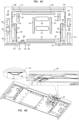
- a point of sale device 100 which includes a housing 102, a keypad 104 and a display 106.
- the housing 102 defines a magnetic stripe card reading slot 108 and a smart card ingress slit 110 which communicates with a smart card receiving slot 112.
- secure smart card connector assembly 120 Disposed within housing 102 is a secure smart card connector assembly 120, which is preferably mounted on a printed circuit board 122. It is a particular feature of the present invention that secure smart card connector assembly 120 includes an anti-tampering mechanism which minimizes exposure of smart card reading contacts to physical tampering and preferably also provides a warning of attempted tampering with the smart card reading contacts.
- this anti-tampering mechanism includes a smart card contact position sensor 130, such as an optical sensor or a mechanical sensor, which is operative to sense when the smart card contacts are in a tamperable orientation. Smart card contact position sensor 130 may be, for example, mechanical or optical.
- the anti-tampering mechanism also includes a card full insertion sensor 132 (shown in dashed lines in Fig. 1 ), which is operative to sense when a card is not fully inserted into smart card receiving slot 112.
- the anti-tampering mechanism also includes a tamper alarm circuit 134, operative to provide a tamper alarm indication in response to outputs of the smart card contact position sensor 130 and of the card full insertion sensor 132, indicating that the plurality of smart card contacts are in the tamperable orientation in the absence of a smart card fully inserted into said smart card receiving slot 112.
- Tamper alarm circuit 134 may be embodied in a microprocessor which forms part of a point of sale device and governs the operation thereof.
- Figs. 2A , 2B , 2C , 2D, 2E, 2F and 2G are simplified drawings including, respectively, a perspective view, a top planar view, a bottom planar view, a first side planar view, a second side planar view, a front planar view and a back planar view of the smart card connector assembly 120, which forms part of the point of sale terminal of Fig. 1 , and to Figs. 3A and 3B , which are simplified exploded view illustrations, taken generally in mutually opposite directions, of the smart card connector assembly 120 of Figs. 2A to 2G .
- the smart card connector assembly 120 includes a base element 150, a contact block assembly 160, which is pivotably mounted onto base element 150 and biased by a leaf spring 162, a contact block assembly position sensor 164, which is an embodiment of contact position sensor 130 (Fig. 1A), and which senses the position of the contact block assembly 160 relative to base element 150, and an actuation arm 170, biased by a tension coil spring 172, which governs the position of the contact block assembly 160 relative to base element 150 in response to the presence of a smart card in smart card receiving slot 112.
- Contact block assembly position sensor 164 senses the rotational position of actuation arm 170, which in turn governs the pivotal orientation of the contact block assembly 160, and is typically an optical sensor 164 as shown.
- contact position sensor 130 may be a mechanical sensor or any other suitable type of sensor.
- Figs. 4A, 4B , 4C, 4D , 4E, 4F, 4G and 4H are simplified drawings including, respectively, a perspective view, a top planar view, a bottom planar view, an upwardly-facing interior sectional view, taken along lines IVD - IVD in Fig. 4A , a first side planar view, a second side planar view, a front planar view and a back planar view of base element 150, forming part of the smart card connector assembly 120 of Figs. 2A - 3B .
- Figs. 4A, 4B , 4C, 4D , 4E, 4F, 4G and 4H are simplified drawings including, respectively, a perspective view, a top planar view, a bottom planar view, an upwardly-facing interior sectional view, taken along lines IVD - IVD in Fig. 4A , a first side planar view, a second side planar view, a front planar view and a back planar view of base
- base element 150 is a generally rectangular element having a top wall portion 200, a bottom wall portion 210, first and second side wall portions 220 and 230, a rear wall portion 240 and a front wall portion 250, which defines a smart card access slit 252 which lies behind and is aligned with smart card ingress slit 110 ( Fig. 1 ) and leads to smart card receiving slot 112, which is defined by interior surfaces of top wall portion 200, bottom wall portion 210, first and second side wall portions 220 and 230 and rear wall portion 240.
- top wall portion 200 includes a central aperture 254, a first side aperture 260 and a second side aperture 270. Top wall portion 200 also includes a relatively long slit aperture 272 and a pair of relatively short slit apertures 274 and 276. Additionally, top wall portion 200 includes first, second, third and fourth upwardly facing tapered elongate recesses, respectively designated by reference numerals 278, 280, 282 and 284. Further, top wall portion 200 includes first, second, third, fourth and fifth upwardly facing elongate recesses having rounded corners, respectively designated by reference numerals 288, 290, 292, 294 and 296.
- top wall portion 200 additionally includes a plurality of relatively large square recesses 298, arranged in a row, a plurality of relatively small square recesses 300, a plurality of relatively large circular recesses 302 and a plurality of relatively small circular recesses 304.
- an upstanding wall portion 306 is provided and includes a central portion 308, a pair of side portions 310 extending perpendicularly to central portion 308, a pair of intermediate portions 312 extending mutually inwardly from respective side portions 310, parallel to central portion 308, and a pair of end portions 314 extending from intermediate portions 312 perpendicularly to central portion 308.
- Upstanding wall portion 306 defines a socket 315, which accommodates leaf spring 162.
- bottom wall portion 210 includes four side apertures 350, 352, 354 and 356.
- Bottom wall portion 210 also includes a pair of mutually spaced U-shaped slits 360 and 362, which surround respective integrally formed spring fingers 364 and 366.
- Bottom wall portion 210 additionally includes two pairs of mutually spaced parallel slits 370 and 372 which surround respective integrally formed elongate leaf springs 374 and 376.
- bottom wall portion 210 includes a pair of relatively short slit apertures 384 and 386. Additionally, bottom wall portion 210 includes a plurality of additional apertures designated by reference numerals 388, 390, 392, 394, 396, 398, 400 and 402.
- Bottom wall portion 210 includes first, second, third, fourth, fifth and sixth downwardly facing elongate shallow protrusions, respectively designated by reference numerals 418, 420, 422, 424, 426 and 428 and four downwardly facing leg protrusions 430.
- a card full insertion sensor 132 ( Fig. 1 ), in the form of a card present switch assembly 440, which preferably includes a resilient card engagement bent finger 442.
- Bent finger 442 is preferably integrally formed with a generally planar mounting portion 446, which is mounted onto an inside facing surface of top wall portion 200 of base element 150.
- Bent finger 442 is normally spaced from an electrically conductive contact 447, preferably in the form of a dome, which is also mounted on an inside facing surface of top wall portion 200, and overlies a pair of mutually spaced electrical conductor pads, preferably, respectively, a central disk 448 surrounded by a ring 449, which is preferably electrically connected to contact 447.
- Disk 448 and ring 449 are preferably electrically connected by conductors (not shown) via respective edge contacts 450 and 452 ( Fig. 4C ) to tamper alarm circuit 134, wherein closing of an electric circuit between disk 448 and ring 449 provides a smart card fully inserted output indication.
- Figs. 5A, 5B , 5C, 5D , 5E , 5F and 5G are simplified drawings including respectively a perspective view, a top planar view, a bottom planar view, a first side planar view, a second side planar view, a front planar view and a back planar view of contact block assembly 160, forming part of the smart card connector of Figs. 2A - 3B , to Figs. 6A and 6B , which are simplified exploded view illustrations, taken generally in mutually opposite directions, of the contact block assembly of Figs. 5A - 5G , and to Figs. 7A - 10B , which illustrate elements of the contact block assembly 160.
- contact block assembly160 includes a plurality of electrical contact elements 500, including at least one I/O contact 501, which are flexibly seated in an electrical contact element support 502 and electrically connected, as by soldering, to corresponding contact pads 504 on a flexible printed circuit element 506.
- a cam path defining element 508 is supported on electrical contact element support 502 and overlies part of flexible printed circuit element 506.
- each electrical contact element 500 is a metal element, preferably formed by stamping, and preferably includes a contact pad portion 520, which is configured for soldered attachment to a contact pad 504 on flexible printed circuit element 506.
- a bent-over tail portion 522 connects contact pad portion 520 to a smart card contact engageable portion 524.
- smart card contact engageable portion 524 is configured to be without a hook engageable surface, so as to be resistant to engagement therewith and pulling thereof by a tampering instrument inserted into the smart card ingress slit 110 ( Fig. 1 ).
- Smart card contact engageable portion 524 is preferably a side to side symmetric, generally hollow portion having an overall partial disk-like configuration and having a curved outer surface 526.
- the curved outer surface 526 includes a curved, ribbon-like smart card contact engagement surface 530, which extends from bent-over tail portion 522 to a forward end of a top edge 532 of smart card contact engageable portion 524.
- Smart card contact engagement surface 530 preferably has an overall circular configuration and preferably has a curved cross section, as seen in a sectional illustration forming part of Fig. 7A , taken along the lines A-A in Fig. 7A .
- Curved outer surface 526 also includes a pair of curved side surfaces 534 alongside both sides of smart card contact engagement surface 530. Curved outer surface 526 additionally includes a pair of generally flat side surfaces 536, which extend between curved side surfaces 534 and top edge 532.
- electrical contact element support 502 is a generally planar element, preferably injection molded of plastic to define at a first end thereof a pivot axle 550 extending along a pivot axis 552 and including an array of elongate recesses 554, preferably eight in number, each recess configured for accommodating an electrical contact element 500.
- Electrical contact element support 502 preferably defines at an end thereof opposite to that at which pivot axle 550 is located, a lip portion 560, which is engaged on an underside surface 562 thereof by leaf spring 162 for normally urging electrical contact element support 502 and thus contact block assembly 160 and electrical contact elements 500 into an upwardly pivoted operative orientation, which is resistant to tampering, when a smart card is not fully inserted into smart card receiving slot 112.
- flexible printed circuit element 506 includes contact pads 504 on a main portion thereof 570.
- Flexible printed circuit element 506 also preferably includes an intermediate portion 572 and a tail portion 574 having formed adjacent an edge thereof an array of electrical contact pads 576.
- cam path defining element 508 is a generally planar element having a generally planar top surface 579, which is formed with a partially recessed, partially protruding cam surface 580.
- Cam surface 580 includes three regions, a recessed region 582 having a uniform depth and a region 584 angled with respect to recessed region 582 and defining a ramp extending from recessed region 582 to a protruding region 586, having a uniform height.
- Figs. 11A , 11B , 11C , 11D, 11E, 11F and 11G are simplified drawings including, respectively, a perspective view, a top planar view, a bottom planar view, a first side planar view, a second side planar view, a front planar view and a back planar view of actuation arm 170, forming part of the smart card connector of Figs. 2A - 3B .
- actuation arm 170 comprises first and second elongate arm portions 600 and 602 which extend in a first plane preferably at right angles to each other.
- a pivot aperture 604 is located at the junction of arm portions 600 and 602 and is arranged for pivotable engagement with upwardly facing protrusion 316 of base element 150.
- Arm portion 600 terminates in a generally cylindrical payment card engagement protrusion 606, which depends from arm portion 600.
- Extending sideways and somewhat upwardly from arm portion 600 at an intermediate location therealong is an apertured spring engagement portion 608, which is arranged to be engaged by tension coil spring 172.
- Arm portion 602 terminates at one end thereof in a cam arm portion 610, which preferably extends generally perpendicular to arm portion 602 and parallel to arm portion 600 in a second plane, above and parallel to the first plane in which arm portions 600 and 602 are located.
- cam arm portion 610 terminates in a depending tapered cam finger portion 612 having a generally planar cam engagement surface 614, which is configured for slidable engagement with partially recessed, partially protruding cam surface 580 of cam path defining element 508.
- Arm portion 602 terminates at an opposite end thereof in a mechanical sensor toggle engagement finger portion 620, which defines a recess 622 bordered by edge surfaces 624, 626 and 628.
- Edge surface 628 is preferably in the form of a curved fingertip surface of a finger portion 630.
- edge surface 628 and part of edge surface 626 is an optical sensor selectable light reflecting finger portion 632, which lies in a third plane, above and parallel to the first plane in which arm portions 600 and 602 are located and below and parallel to the second plane in which cam portion 610 is located, and extends generally parallel to arm portions 600 and 610.
- FIGS. 12A and 12B are simplified perspective view illustrations illustrating a transition of the smart card connector of Figs. 1 - 11G from a card not inserted state to a card fully inserted state.
- actuation arm 170 is in its at rest position, as seen in Fig. 2A , and light reflecting finger portion 632 does not overlie the optical sensor 164 and thus does not reflect light emitted thereby by an LED 692 to a detector 694 thereof, as seen particularly in enlargement A, which shows a simplified section of optical sensor 164 and a light beam emanating therefrom which is not reflected by finger portion 632.
- optical sensor 164 is in a first logic state, which indicates to tamper alarm circuit 134 that card engagement contacts 500, and specifically at least one I/O contact 501, are in a retracted operative orientation.
- the card present switch assembly 440 In the absence of a card in smart card receiving slot 112, the card present switch assembly 440 is in its at rest position, as seen in Fig. 4D , and the bent finger 442 is spaced from electrically conductive contact 447, as seen particularly in enlargement B, which shows a simplified cross section of the bent finger 442 and electrically conductive contact 447. Bent finger 442 is not resiliently displaced into deforming engagement with electrically conductive contact 447, and central disk 448 is not in electrical contact with ring 449 causing a smart card not inserted output indication to be provided to tamper alarm circuit 134.
- actuation arm 170 In the absence of a card in smart card receiving slot 112, when actuation arm 170 is in its at rest position, the cam finger portion 612 of the actuation arm 170 is in engagement with recessed region 582 of cam surface 580 defined on cam path defining element 508. When in this position, actuation arm 170 preferably does not exert any downward pressure on contact block assembly 160, and thus contact block assembly 160 remains in its upwardly retracted operative orientation, as seen particularly in enlargement C, which is a side view illustration, taken along lines C - C in Fig. 12A .
- leaf spring 162 In the absence of a card in smart card receiving slot 112, when actuation arm 170 is in its at rest position and the cam finger portion 612 of the actuation arm 170 is in engagement with recessed region 582 of cam surface 580 defined on cam path defining element 508, leaf spring 162 is in its extended operative orientation, as seen particularly in enlargement D, which is a cross section taken along lines D - D in Fig. 12A .
- Leaf spring 162 engages underside surface 562 of lip portion 560 of electrical contact element support 502 and thereby urges electrical contact element support 502, and thus contact block assembly 160 and electrical contact elements 500, into their upwardly pivoted operative orientation, which is resistant to tampering.
- Fig. 12B shows the operative orientation of the secure smart card connector assembly 120 when a smart card 690 is fully inserted in smart card receiving slot 112, actuation arm 170 is fully rotated in a clockwise rotation direction 700 about an actuation arm rotation axis 702 defined by protrusion 316 ( Fig. 4A ) which extends through pivot aperture 604 ( Fig. 11A ) from its at rest position, as seen in Figs. 2A and 12A , to a fully rotated position seen in Fig. 12B .
- optical sensor 164 When actuation arm 170 is in this fully rotated position, as seen particularly in enlargement A, light reflecting finger portion 632 overlies the optical sensor 164 and thus a light beam emanating from LED 692 of optical sensor 164 is reflected by finger portion 632 to detector 694 of optical sensor 164. In this situation, optical sensor 164 is in a second logic state, which indicates to tamper alarm circuit 134 that card engagement contacts 500, and specifically at least one I/O contact 501, are in an extended operative orientation.
- bent finger 442 When a smart card 690 is fully inserted into smart card receiving slot 112, bent finger 442 is resiliently displaced into deforming engagement with electrically conductive contact 447, as indicated by an arrow 710, causing it to contact central disk 448, as seen particularly in enlargement B, which shows a simplified cross section of the bent finger 442 and electrically conductive contact 447. Accordingly, an electrical connection is made between disk 448 and ring 449, and thus between edge contacts 450 and 452, thereby providing a smart card fully inserted output indication to tamper alarm circuit 134.
- actuation arm 170 When a smart card 690 is fully inserted in smart card receiving slot 112, and actuation arm 170 is in its fully rotated position, the cam finger portion 612 of the actuation arm 170 is in engagement with protruding region 586 of cam surface 580 defined on cam path defining element 508. When in this position, actuation arm 170 preferably exerts downward pressure on contact block assembly 160, and thus contact block assembly 160 is in its pivotally lowered operative orientation, as seen particularly in enlargement C, which is a side view illustration, taken along lines C- C in Fig. 12B .
- actuation arm 170 When a smart card 690 is fully inserted in smart card receiving slot 112, actuation arm 170 is in its fully rotated position and the cam finger portion 612 of the actuation arm 170 is in engagement with protruding region 586 of cam surface 580 defined on cam path defining element 508. Rotation of actuation arm 170 causes downward pivoting of electrical contact element support 502 which overcomes the upward force of leaf spring 162 and underside surface 562 of lip portion 560 of electrical contact element support 502 compresses leaf spring 162 into a compressed operative orientation, as seen particularly in enlargement D, which is a cross section taken along lines D - D. In the compressed operative orientation, access to electrical contact elements 500 is blocked by the smart card 690, which is fully inserted into smart card receiving slot 112.
- contact block assembly 160 When a smart card 690 is fully inserted in smart card receiving slot 112, contact block assembly 160 is in its pivotally lowered operative orientation and electrical contact elements 500, and specifically at least one I/O contact 501, are at least partly located within smart card receiving slot 112 and in engagement with contact pads 691 on the smart card 690, as seen particularly in enlargement E, which is taken along arrow E. It is a particular feature of an embodiment of the present invention that only in the presence of a card in smart card receiving slot 112, are the electrical contact elements 500, and specifically at least one I/O contact 501, lowered into conductive engagement with contact pads of the card, thereby making it difficult for a potential hacker to engage the electrical contact elements 500.
- FIGs. 13A and 13B are simplified perspective view illustrations illustrating a transition of the smart card connector of an alternative embodiment of the invention from a card not inserted state to a card fully inserted state.
- the alternative embodiment of the invention is generally identical to that described hereinabove with reference to Figs. 1 - 12B with the sole difference being that the optical sensor 164 is replaced by a mechanical sensor 764 having an engagement finger 766.
- actuation arm 170 is in its at rest position and engagement finger 766 of mechanical sensor 764 lies within recess 622 ( Fig. 11C ) of actuation arm 170, as seen particularly in enlargement A, which shows a partially cut away top view of mechanical sensor 764 and recess 622.
- engagement finger 766 is in this orientation, mechanical sensor 764 is in a first logic state, which indicates to tamper alarm circuit 134 that card engagement contacts 500, and specifically at least one I/O contact 501, are in a retracted operative orientation.
- the card present switch assembly 440 In the absence of a card in smart card receiving slot 112, the card present switch assembly 440 is in its at rest position, as seen in Fig. 4D , and the bent finger 442 is spaced from electrically conductive contact 447, as seen particularly in enlargement B, which shows a simplified cross section of the bent finger 442 and electrically conductive contact 447. Bent finger 442 is not resiliently displaced into deforming engagement with electrically conductive contact 447, and central disk 448 is not in electrical contact with ring 449 causing a smart card not inserted output indication to be provided to tamper alarm circuit 134.
- actuation arm 170 In the absence of a card in smart card receiving slot 112, when actuation arm 170 is in its at rest position, the cam finger portion 612 of the actuation arm 170 is in engagement with recessed region 582 of cam surface 580 defined on cam path defining element 508. When in this position, actuation arm 170 preferably does not exert any downward pressure on contact block assembly 160, and thus contact block assembly 160 remains in its upwardly retracted operative orientation, as seen particularly in enlargement C, which is a side view illustration, taken along an arrow C.
- leaf spring 162 In the absence of a card in smart card receiving slot 112, when actuation arm 170 is in its at rest position and the cam finger portion 612 of the actuation arm 170 is in engagement with recessed region 582 of cam surface 580 defined on cam path defining element 508, leaf spring 162 is in its extended operative orientation, as seen particularly in enlargement D, which is a cross section taken along lines D - D in Fig. 13A .
- Leaf spring 162 engages underside surface 562 of lip portion 560 of electrical contact element support 502 and thereby urges electrical contact element support 502, and thus contact block assembly 160 and electrical contact elements 500, into their upwardly pivoted operative orientation, which is resistant to tampering.
- actuation arm 170 is fully rotated in clockwise rotation direction 700 about an actuation arm rotation axis 702 defined by protrusion 316 ( Fig. 4A ) which extends through pivot aperture 604 ( Fig. 11A ) from its at rest position, as seen in Fig. 13A , to a fully rotated position seen in Fig. 13B .
- engagement finger 766 of mechanical sensor 764 lies outside recess 622 ( Fig.
- actuation arm 170 engages edge surface 628 of finger portion 630 of actuation arm 170, as seen particularly in enlargement A, which shows a partially cut away top view of mechanical sensor 764 and recess 622. It is seen that engagement finger 766 has been pivoted relative to the remainder of mechanical sensor 764, such that the mechanical sensor is in a second logic state which indicates that electrical contact elements 500, and specifically at least one I/O contact 501, are in an extended state.
- bent finger 442 When a smart card 690 is fully inserted into smart card receiving slot 112, bent finger 442 is resiliently displaced into deforming engagement with electrically conductive contact 447, as indicated by an arrow 770, causing it to contact central disk 448, as seen particularly in enlargement B, which shows a simplified cross section of the bent finger 442 and electrically conductive contact 447. Accordingly an electrical connection is made between disk 448 and ring 449, and thus between edge contacts 450 and 452, thereby providing a smart card fully inserted output indication to tamper alarm circuit 134.
- actuation arm 170 When a smart card 690 is fully inserted in smart card receiving slot 112, when actuation arm 170 is in its fully rotated position, the cam finger portion 612 of the actuation arm 170 is in engagement with protruding region 586 of cam surface 580 defined on cam path defining element 508. When in this position, actuation arm 170 preferably exerts downward pressure on contact block assembly 160, and thus contact block assembly 160 is in its pivotally lowered operative orientation, as seen particularly in enlargement C, which is a side view illustration, taken along line C - C.
- actuation arm 170 When a smart card 690 is fully inserted in smart card receiving slot 112, actuation arm 170 is in its fully rotated position and the cam finger portion 612 of the actuation arm 170 is in engagement with protruding region 586 of cam surface 580 defined on cam path defining element 508. Rotation of actuation arm 170 causes downward pivoting of electrical contact element support 502 which overcomes the upward force of leaf spring 162 and underside surface 562 of lip portion 560 of electrical contact element support 502 compresses leaf spring 162 into a compressed operative orientation, as seen particularly in enlargement D, which is a cross section taken along lines D - D in Fig. 13B . In the compressed operative orientation, access to electrical contact elements 500 is blocked by the smart card 690, which is fully inserted into smart card receiving slot 112.
- electrical contact elements 500 When a smart card 690 is fully inserted in smart card receiving slot 112, when contact block assembly 160 is in its pivotally lowered operative orientation, electrical contact elements 500, and specifically at least one I/O contact 501, are at least partly located within smart card receiving slot 112 and in engagement with contact pads 691 on the smart card 690, as seen particularly in enlargement E, which is taken along arrow E. It is a particular feature of an embodiment of the present invention that only in the presence of a card in smart card receiving slot 112, are the electrical contact elements 500, and specifically at least one I/O contact 501, lowered into conductive engagement with contact pads of the card, thereby making it difficult for a potential hacker to engage the electrical contact elements 500.
- an alarm is provided when electrical contact elements 500 are extended into the smart card receiving slot 112 in the absence of a card fully inserted into smart card receiving slot 112.
- tamper alarm circuit 134 may be designed as summarized below ... CARD PRESENT IN SLOT CONTACT ELEMENTS EXTENDED INTO SLOT ALARM YES/NO (SENSOR 132) (SENSOR 130) YES NO YES YES YES NO NO NO NO NO NO YES YES
Landscapes
- Engineering & Computer Science (AREA)
- Physics & Mathematics (AREA)
- General Physics & Mathematics (AREA)
- Artificial Intelligence (AREA)
- Computer Vision & Pattern Recognition (AREA)
- Theoretical Computer Science (AREA)
- Business, Economics & Management (AREA)
- Emergency Management (AREA)
- Microelectronics & Electronic Packaging (AREA)
- Details Of Connecting Devices For Male And Female Coupling (AREA)
- Coupling Device And Connection With Printed Circuit (AREA)
Description
- The invention relates to data entry devices generally, particularly to point of sale terminals and more particularly to smart card connector assemblies for point of sale terminals.
- Various types of smart card connector assemblies for point of sale terminals are known.
-
FR 2 792 437 US 2015/0213334 ,US 2005/0218227 ,US 5,563,397 ,US 5,045,674 ,US 2001/ 014549 US 6,210,193 andUS 4,904,852 disclose aspects of such smart card connectors assemblies. - The invention seeks to provide improved smart card connector assemblies for point of sale terminals.
- There is thus provided a smart card as defined by the claims.
- When the at least one of the plurality of smart card contacts is in the first position it is relatively inaccessible to tampering via the smart card ingress slit. This is to say that the smart card contacts in the first position are less accessible to tampering than in the second position.
- The invention will be understood and appreciated more fully from the following detailed description, taken in conjunction with the drawings.
-
Fig. 1 is a simplified pictorial illustration of a point of sale terminal constructed and operative in accordance with a preferred embodiment of the present invention; -
Figs. 2A ,2B ,2C ,2D, 2E, 2F and 2G are simplified drawings including, respectively, a perspective view, a top planar view, a bottom planar view, a first side planar view, a second side planar view, a front planar view and a back planar view of a smart card connector assembly constructed and operative in accordance with a preferred embodiment of the invention, which forms part of the point of sale terminal ofFig. 1 and includes an optical sensor; -
Figs. 3A and 3B are simplified exploded view illustrations, taken generally in mutually opposite directions, of the smart card connector assembly ofFigs. 2A to 2G ; -
Figs. 4A, 4B ,4C, 4D ,4E, 4F, 4G and 4H are simplified drawings including, respectively, a perspective view, a top planar view, a bottom planar view, an upwardly-facing interior sectional view, taken along lines IVD - IVD inFig. 4A , a first side planar view, a second side planar view, a front planar view and a back planar view of a base element forming part of the smart card connector ofFigs. 2A to 3B ; -
Figs. 5A, 5B ,5C, 5D ,5E ,5F and 5G are simplified drawings including, respectively, a perspective view, a top planar view, a bottom planar view, a first side planar view, a second side planar view, a front planar view and a back planar view of a contact block assembly forming part of the smart card connector ofFigs. 2A to 3B ; -
Figs. 6A and6B are simplified exploded view illustrations, taken generally in mutually opposite directions, of the contact block assembly ofFigs. 5A to 5G ; -
Figs. 7A ,7B, 7C, 7D ,7E ,7F and 7G are simplified drawings including, respectively, a perspective view, a top planar view, a bottom planar view, a first side planar view, a second side planar view, a front planar view and a back planar view of an electrical contact element forming part of the contact block assembly ofFigs. 5A to 6B ; -
Figs. 8A ,8B, 8C, 8D ,8E ,8F and 8G are simplified drawings including, respectively, a perspective view, a top planar view, a bottom planar view, a first side planar view, a second side planar view, a front planar view and a back planar view of an electrical contact element support forming part of the contact block assembly ofFigs. 5A to 6B ; -
Figs. 9A ,9B and 9C are simplified drawings including, respectively, a perspective view, a top planar view and a bottom planar view of a flexible printed circuit element forming part of the contact block assembly ofFigs. 5A to 6B ; -
Figs. 10A ,10B, 10C, 10D ,10E ,10F and 10G are, respectively, a perspective view, a top planar view, a bottom planar view, a first side planar view, a second side planar view, a front planar view and a back planar view of a cam path defining element forming part of the contact block assembly ofFigs. 5A to 6B ; -
Figs. 11A ,11B ,11C ,11D, 11E, 11F and 11G are simplified drawings including, respectively, a perspective view, a top planar view, a bottom planar view, a first side planar view, a second side planar view, a front planar view and a back planar view of an actuation arm forming part of the smart card connector ofFigs. 2A to 3B ; -
Figs. 12A and12B are simplified perspective view illustrations illustrating a transition of the smart card connector ofFigs. 1to 11G from a card not inserted state to a card fully inserted state; and -
Figs. 13A and13B are simplified perspective view illustrations illustrating a transition of an alternative embodiment of the smart card connector ofFigs. 1 to 11G from a card not inserted state to a card fully inserted state. - Reference is now made to
Fig. 1 , which is a simplified pictorial illustration of a point of sale terminal constructed and operative in accordance with a preferred embodiment of the present invention. As seen inFig. 1 , there is provided a point ofsale device 100, which includes ahousing 102, akeypad 104 and adisplay 106. Preferably, thehousing 102 defines a magnetic stripecard reading slot 108 and a smartcard ingress slit 110 which communicates with a smartcard receiving slot 112. - Disposed within
housing 102 is a secure smartcard connector assembly 120, which is preferably mounted on a printedcircuit board 122. It is a particular feature of the present invention that secure smartcard connector assembly 120 includes an anti-tampering mechanism which minimizes exposure of smart card reading contacts to physical tampering and preferably also provides a warning of attempted tampering with the smart card reading contacts. Preferably, this anti-tampering mechanism includes a smart cardcontact position sensor 130, such as an optical sensor or a mechanical sensor, which is operative to sense when the smart card contacts are in a tamperable orientation. Smart cardcontact position sensor 130 may be, for example, mechanical or optical. - The anti-tampering mechanism also includes a card full insertion sensor 132 (shown in dashed lines in
Fig. 1 ), which is operative to sense when a card is not fully inserted into smartcard receiving slot 112. - The anti-tampering mechanism also includes a
tamper alarm circuit 134, operative to provide a tamper alarm indication in response to outputs of the smart cardcontact position sensor 130 and of the cardfull insertion sensor 132, indicating that the plurality of smart card contacts are in the tamperable orientation in the absence of a smart card fully inserted into said smartcard receiving slot 112.Tamper alarm circuit 134 may be embodied in a microprocessor which forms part of a point of sale device and governs the operation thereof. - Reference is now additionally made to
Figs. 2A ,2B ,2C ,2D, 2E, 2F and 2G , which are simplified drawings including, respectively, a perspective view, a top planar view, a bottom planar view, a first side planar view, a second side planar view, a front planar view and a back planar view of the smartcard connector assembly 120, which forms part of the point of sale terminal ofFig. 1 , and toFigs. 3A and 3B , which are simplified exploded view illustrations, taken generally in mutually opposite directions, of the smartcard connector assembly 120 ofFigs. 2A to 2G . - As seen in
Figs. 2A - 3B , the smartcard connector assembly 120 includes abase element 150, acontact block assembly 160, which is pivotably mounted ontobase element 150 and biased by aleaf spring 162, a contact blockassembly position sensor 164, which is an embodiment of contact position sensor 130 (Fig. 1A), and which senses the position of thecontact block assembly 160 relative tobase element 150, and anactuation arm 170, biased by atension coil spring 172, which governs the position of thecontact block assembly 160 relative tobase element 150 in response to the presence of a smart card in smartcard receiving slot 112. Contact blockassembly position sensor 164 senses the rotational position ofactuation arm 170, which in turn governs the pivotal orientation of thecontact block assembly 160, and is typically anoptical sensor 164 as shown. Alternatively,contact position sensor 130 may be a mechanical sensor or any other suitable type of sensor. - Reference is now additionally made to
Figs. 4A, 4B ,4C, 4D ,4E, 4F, 4G and 4H , which are simplified drawings including, respectively, a perspective view, a top planar view, a bottom planar view, an upwardly-facing interior sectional view, taken along lines IVD - IVD inFig. 4A , a first side planar view, a second side planar view, a front planar view and a back planar view ofbase element 150, forming part of the smartcard connector assembly 120 ofFigs. 2A - 3B . As seen inFigs. 4A - 4H ,base element 150 is a generally rectangular element having atop wall portion 200, abottom wall portion 210, first and secondside wall portions rear wall portion 240 and afront wall portion 250, which defines a smart card access slit 252 which lies behind and is aligned with smart card ingress slit 110 (Fig. 1 ) and leads to smartcard receiving slot 112, which is defined by interior surfaces oftop wall portion 200,bottom wall portion 210, first and secondside wall portions rear wall portion 240. - As seen particularly in
Figs. 4A and 4B ,top wall portion 200 includes acentral aperture 254, afirst side aperture 260 and asecond side aperture 270.Top wall portion 200 also includes a relativelylong slit aperture 272 and a pair of relativelyshort slit apertures top wall portion 200 includes first, second, third and fourth upwardly facing tapered elongate recesses, respectively designated byreference numerals top wall portion 200 includes first, second, third, fourth and fifth upwardly facing elongate recesses having rounded corners, respectively designated byreference numerals - It is also seen that
top wall portion 200 additionally includes a plurality of relatively largesquare recesses 298, arranged in a row, a plurality of relatively smallsquare recesses 300, a plurality of relatively largecircular recesses 302 and a plurality of relatively smallcircular recesses 304. It is further seen that anupstanding wall portion 306 is provided and includes acentral portion 308, a pair ofside portions 310 extending perpendicularly tocentral portion 308, a pair ofintermediate portions 312 extending mutually inwardly fromrespective side portions 310, parallel tocentral portion 308, and a pair ofend portions 314 extending fromintermediate portions 312 perpendicularly tocentral portion 308.Upstanding wall portion 306 defines asocket 315, which accommodatesleaf spring 162. - It is additionally seen that there are provided three generally circular cylindrical upwardly facing protrusions, respectively designated by
reference numerals - As seen particularly in
Fig. 4C ,bottom wall portion 210 includes fourside apertures Bottom wall portion 210 also includes a pair of mutually spacedU-shaped slits spring fingers Bottom wall portion 210 additionally includes two pairs of mutually spacedparallel slits elongate leaf springs - Additionally,
bottom wall portion 210 includes a pair of relativelyshort slit apertures bottom wall portion 210 includes a plurality of additional apertures designated byreference numerals -
Bottom wall portion 210 includes first, second, third, fourth, fifth and sixth downwardly facing elongate shallow protrusions, respectively designated byreference numerals leg protrusions 430. - As seen particularly in
Fig. 4D , there is provided a preferred embodiment of a card full insertion sensor 132 (Fig. 1 ), in the form of a cardpresent switch assembly 440, which preferably includes a resilient card engagementbent finger 442.Bent finger 442 is preferably integrally formed with a generally planar mountingportion 446, which is mounted onto an inside facing surface oftop wall portion 200 ofbase element 150.Bent finger 442 is normally spaced from an electricallyconductive contact 447, preferably in the form of a dome, which is also mounted on an inside facing surface oftop wall portion 200, and overlies a pair of mutually spaced electrical conductor pads, preferably, respectively, acentral disk 448 surrounded by aring 449, which is preferably electrically connected to contact 447. -
Disk 448 andring 449 are preferably electrically connected by conductors (not shown) viarespective edge contacts 450 and 452 (Fig. 4C ) to tamperalarm circuit 134, wherein closing of an electric circuit betweendisk 448 andring 449 provides a smart card fully inserted output indication. - Reference is now made to
Figs. 5A, 5B ,5C, 5D ,5E ,5F and 5G , which are simplified drawings including respectively a perspective view, a top planar view, a bottom planar view, a first side planar view, a second side planar view, a front planar view and a back planar view ofcontact block assembly 160, forming part of the smart card connector ofFigs. 2A - 3B , toFigs. 6A and6B , which are simplified exploded view illustrations, taken generally in mutually opposite directions, of the contact block assembly ofFigs. 5A - 5G , and toFigs. 7A - 10B , which illustrate elements of thecontact block assembly 160. - As seen in
Figs. 5A - 6B , contact block assembly160 includes a plurality ofelectrical contact elements 500, including at least one I/O contact 501, which are flexibly seated in an electricalcontact element support 502 and electrically connected, as by soldering, tocorresponding contact pads 504 on a flexible printedcircuit element 506. A campath defining element 508 is supported on electricalcontact element support 502 and overlies part of flexible printedcircuit element 506. - Referring additionally to
Figs. 7A - 7G , it is seen that eachelectrical contact element 500 is a metal element, preferably formed by stamping, and preferably includes acontact pad portion 520, which is configured for soldered attachment to acontact pad 504 on flexible printedcircuit element 506. A bent-overtail portion 522 connectscontact pad portion 520 to a smart card contactengageable portion 524. It is a particular feature of an embodiment of the present invention that smart card contactengageable portion 524 is configured to be without a hook engageable surface, so as to be resistant to engagement therewith and pulling thereof by a tampering instrument inserted into the smart card ingress slit 110 (Fig. 1 ). - Smart card contact
engageable portion 524 is preferably a side to side symmetric, generally hollow portion having an overall partial disk-like configuration and having a curvedouter surface 526. Preferably, the curvedouter surface 526 includes a curved, ribbon-like smart cardcontact engagement surface 530, which extends from bent-overtail portion 522 to a forward end of atop edge 532 of smart card contactengageable portion 524. Smart cardcontact engagement surface 530 preferably has an overall circular configuration and preferably has a curved cross section, as seen in a sectional illustration forming part ofFig. 7A , taken along the lines A-A inFig. 7A . - Curved
outer surface 526 also includes a pair of curved side surfaces 534 alongside both sides of smart cardcontact engagement surface 530. Curvedouter surface 526 additionally includes a pair of generally flat side surfaces 536, which extend between curved side surfaces 534 andtop edge 532. - Referring now specifically to
Figs. 8A - 8G , it is seen that electricalcontact element support 502 is a generally planar element, preferably injection molded of plastic to define at a first end thereof apivot axle 550 extending along apivot axis 552 and including an array ofelongate recesses 554, preferably eight in number, each recess configured for accommodating anelectrical contact element 500. Electricalcontact element support 502 preferably defines at an end thereof opposite to that at whichpivot axle 550 is located, alip portion 560, which is engaged on anunderside surface 562 thereof byleaf spring 162 for normally urging electricalcontact element support 502 and thus contactblock assembly 160 andelectrical contact elements 500 into an upwardly pivoted operative orientation, which is resistant to tampering, when a smart card is not fully inserted into smartcard receiving slot 112. - Referring now specifically to
Figs. 9A ,9B and 9C , it is seen that flexible printedcircuit element 506 includescontact pads 504 on amain portion thereof 570. Flexible printedcircuit element 506 also preferably includes anintermediate portion 572 and atail portion 574 having formed adjacent an edge thereof an array ofelectrical contact pads 576. - Referring now specifically to
Figs. 10A ,10B, 10C, 10D ,10E ,10F and 10G , which are, respectively, a perspective view, a top planar view, a bottom planar view, a first side planar view, a second side planar view, a front planar view and a back planar view of campath defining element 508, it is seen that campath defining element 508 is a generally planar element having a generally planartop surface 579, which is formed with a partially recessed, partially protrudingcam surface 580.Cam surface 580 includes three regions, a recessedregion 582 having a uniform depth and aregion 584 angled with respect to recessedregion 582 and defining a ramp extending from recessedregion 582 to aprotruding region 586, having a uniform height. - Reference is now made to
Figs. 11A ,11B ,11C ,11D, 11E, 11F and 11G , which are simplified drawings including, respectively, a perspective view, a top planar view, a bottom planar view, a first side planar view, a second side planar view, a front planar view and a back planar view ofactuation arm 170, forming part of the smart card connector ofFigs. 2A - 3B . - As seen in
Figs. 11A - 11G ,actuation arm 170 comprises first and secondelongate arm portions pivot aperture 604 is located at the junction ofarm portions protrusion 316 ofbase element 150.Arm portion 600 terminates in a generally cylindrical paymentcard engagement protrusion 606, which depends fromarm portion 600. Extending sideways and somewhat upwardly fromarm portion 600 at an intermediate location therealong is an aperturedspring engagement portion 608, which is arranged to be engaged bytension coil spring 172. -
Arm portion 602 terminates at one end thereof in acam arm portion 610, which preferably extends generally perpendicular toarm portion 602 and parallel toarm portion 600 in a second plane, above and parallel to the first plane in which armportions Fig. 11C ,cam arm portion 610 terminates in a depending taperedcam finger portion 612 having a generally planarcam engagement surface 614, which is configured for slidable engagement with partially recessed, partially protrudingcam surface 580 of campath defining element 508. -
Arm portion 602 terminates at an opposite end thereof in a mechanical sensor toggleengagement finger portion 620, which defines arecess 622 bordered byedge surfaces Edge surface 628 is preferably in the form of a curved fingertip surface of afinger portion 630. -
Overlying finger portion 630,edge surface 628 and part ofedge surface 626 is an optical sensor selectable light reflectingfinger portion 632, which lies in a third plane, above and parallel to the first plane in which armportions cam portion 610 is located, and extends generally parallel to armportions - Reference is now made to
Figs. 12A and12B , which are simplified perspective view illustrations illustrating a transition of the smart card connector ofFigs. 1 - 11G from a card not inserted state to a card fully inserted state. - As seen in
Fig. 12A , where asmart card 690 havingcontact pads 691 is located outside of smartcard receiving slot 112,actuation arm 170 is in its at rest position, as seen inFig. 2A , and light reflectingfinger portion 632 does not overlie theoptical sensor 164 and thus does not reflect light emitted thereby by anLED 692 to adetector 694 thereof, as seen particularly in enlargement A, which shows a simplified section ofoptical sensor 164 and a light beam emanating therefrom which is not reflected byfinger portion 632. In this situation,optical sensor 164 is in a first logic state, which indicates to tamperalarm circuit 134 thatcard engagement contacts 500, and specifically at least one I/O contact 501, are in a retracted operative orientation. - In the absence of a card in smart
card receiving slot 112, the cardpresent switch assembly 440 is in its at rest position, as seen inFig. 4D , and thebent finger 442 is spaced from electricallyconductive contact 447, as seen particularly in enlargement B, which shows a simplified cross section of thebent finger 442 and electricallyconductive contact 447.Bent finger 442 is not resiliently displaced into deforming engagement with electricallyconductive contact 447, andcentral disk 448 is not in electrical contact withring 449 causing a smart card not inserted output indication to be provided to tamperalarm circuit 134. - In the absence of a card in smart
card receiving slot 112, whenactuation arm 170 is in its at rest position, thecam finger portion 612 of theactuation arm 170 is in engagement with recessedregion 582 ofcam surface 580 defined on campath defining element 508. When in this position,actuation arm 170 preferably does not exert any downward pressure oncontact block assembly 160, and thus contactblock assembly 160 remains in its upwardly retracted operative orientation, as seen particularly in enlargement C, which is a side view illustration, taken along lines C - C inFig. 12A . - In the absence of a card in smart
card receiving slot 112, whenactuation arm 170 is in its at rest position and thecam finger portion 612 of theactuation arm 170 is in engagement with recessedregion 582 ofcam surface 580 defined on campath defining element 508,leaf spring 162 is in its extended operative orientation, as seen particularly in enlargement D, which is a cross section taken along lines D - D inFig. 12A .Leaf spring 162 engagesunderside surface 562 oflip portion 560 of electricalcontact element support 502 and thereby urges electricalcontact element support 502, and thus contactblock assembly 160 andelectrical contact elements 500, into their upwardly pivoted operative orientation, which is resistant to tampering. - In the absence of a
smart card 690 in smartcard receiving slot 112, whencontact block assembly 160 is in its upwardly retracted operative orientation,electrical contact elements 500, and specifically at least one I/O contact 501, are nearly completely retracted upwardly out of smartcard receiving slot 112, as seen particularly in enlargement E, which is taken along arrow E. It is a particular feature of an embodiment of the present invention that in the absence of a card in smartcard receiving slot 112, theelectrical contact elements 500, and specifically at least one I/O contact 501, are nearly completely retracted upwardly out of smartcard receiving slot 112, thereby making it difficult for a potential hacker to engage theelectrical contact elements 500. - It is a further particular feature of an embodiment of the present invention that in addition to the retraction of the
electrical contact elements 500 when a card is not fully inserted into smartcard receiving slot 112, the particular configuration of theelectrical contact elements 500, so as to be without a hook engageable surface, makes it difficult to tamper with theelectrical contact elements 500 in general and the one or more I/O contact elements 501 in particular. - Turning now to
Fig. 12B , which shows the operative orientation of the secure smartcard connector assembly 120 when asmart card 690 is fully inserted in smartcard receiving slot 112,actuation arm 170 is fully rotated in aclockwise rotation direction 700 about an actuationarm rotation axis 702 defined by protrusion 316 (Fig. 4A ) which extends through pivot aperture 604 (Fig. 11A ) from its at rest position, as seen inFigs. 2A and12A , to a fully rotated position seen inFig. 12B . Whenactuation arm 170 is in this fully rotated position, as seen particularly in enlargement A, light reflectingfinger portion 632 overlies theoptical sensor 164 and thus a light beam emanating fromLED 692 ofoptical sensor 164 is reflected byfinger portion 632 todetector 694 ofoptical sensor 164. In this situation,optical sensor 164 is in a second logic state, which indicates to tamperalarm circuit 134 thatcard engagement contacts 500, and specifically at least one I/O contact 501, are in an extended operative orientation. - When a
smart card 690 is fully inserted into smartcard receiving slot 112,bent finger 442 is resiliently displaced into deforming engagement with electricallyconductive contact 447, as indicated by anarrow 710, causing it to contactcentral disk 448, as seen particularly in enlargement B, which shows a simplified cross section of thebent finger 442 and electricallyconductive contact 447. Accordingly, an electrical connection is made betweendisk 448 andring 449, and thus betweenedge contacts alarm circuit 134. - When a
smart card 690 is fully inserted in smartcard receiving slot 112, andactuation arm 170 is in its fully rotated position, thecam finger portion 612 of theactuation arm 170 is in engagement with protrudingregion 586 ofcam surface 580 defined on campath defining element 508. When in this position,actuation arm 170 preferably exerts downward pressure oncontact block assembly 160, and thus contactblock assembly 160 is in its pivotally lowered operative orientation, as seen particularly in enlargement C, which is a side view illustration, taken along lines C- C inFig. 12B . - When a
smart card 690 is fully inserted in smartcard receiving slot 112,actuation arm 170 is in its fully rotated position and thecam finger portion 612 of theactuation arm 170 is in engagement with protrudingregion 586 ofcam surface 580 defined on campath defining element 508. Rotation ofactuation arm 170 causes downward pivoting of electricalcontact element support 502 which overcomes the upward force ofleaf spring 162 andunderside surface 562 oflip portion 560 of electricalcontact element support 502 compressesleaf spring 162 into a compressed operative orientation, as seen particularly in enlargement D, which is a cross section taken along lines D - D. In the compressed operative orientation, access toelectrical contact elements 500 is blocked by thesmart card 690, which is fully inserted into smartcard receiving slot 112. - When a
smart card 690 is fully inserted in smartcard receiving slot 112,contact block assembly 160 is in its pivotally lowered operative orientation andelectrical contact elements 500, and specifically at least one I/O contact 501, are at least partly located within smartcard receiving slot 112 and in engagement withcontact pads 691 on thesmart card 690, as seen particularly in enlargement E, which is taken along arrow E. It is a particular feature of an embodiment of the present invention that only in the presence of a card in smartcard receiving slot 112, are theelectrical contact elements 500, and specifically at least one I/O contact 501, lowered into conductive engagement with contact pads of the card, thereby making it difficult for a potential hacker to engage theelectrical contact elements 500. - It is a further particular feature of an embodiment of the present invention that in addition to the lowering and extension of the
electrical contact elements 500 into the smartcard receiving slot 112 only when a smart card is fully inserted into smartcard receiving slot 112, the particular configuration of theelectrical contact elements 500, so as to be without a hook engageable surface, makes it difficult to tamper with theelectrical contact elements 500 in general and the one or more I/O contact elements 501 in particular. - Reference is now made to
Figs. 13A and13B , which are simplified perspective view illustrations illustrating a transition of the smart card connector of an alternative embodiment of the invention from a card not inserted state to a card fully inserted state. The alternative embodiment of the invention is generally identical to that described hereinabove with reference toFigs. 1 - 12B with the sole difference being that theoptical sensor 164 is replaced by amechanical sensor 764 having anengagement finger 766. - As seen in
Fig. 13A , where asmart card 690 havingcontact pads 691 is located outside of smartcard receiving slot 112,actuation arm 170 is in its at rest position andengagement finger 766 ofmechanical sensor 764 lies within recess 622 (Fig. 11C ) ofactuation arm 170, as seen particularly in enlargement A, which shows a partially cut away top view ofmechanical sensor 764 andrecess 622. Whenengagement finger 766 is in this orientation,mechanical sensor 764 is in a first logic state, which indicates to tamperalarm circuit 134 thatcard engagement contacts 500, and specifically at least one I/O contact 501, are in a retracted operative orientation. - In the absence of a card in smart
card receiving slot 112, the cardpresent switch assembly 440 is in its at rest position, as seen inFig. 4D , and thebent finger 442 is spaced from electricallyconductive contact 447, as seen particularly in enlargement B, which shows a simplified cross section of thebent finger 442 and electricallyconductive contact 447.Bent finger 442 is not resiliently displaced into deforming engagement with electricallyconductive contact 447, andcentral disk 448 is not in electrical contact withring 449 causing a smart card not inserted output indication to be provided to tamperalarm circuit 134. - In the absence of a card in smart
card receiving slot 112, whenactuation arm 170 is in its at rest position, thecam finger portion 612 of theactuation arm 170 is in engagement with recessedregion 582 ofcam surface 580 defined on campath defining element 508. When in this position,actuation arm 170 preferably does not exert any downward pressure oncontact block assembly 160, and thus contactblock assembly 160 remains in its upwardly retracted operative orientation, as seen particularly in enlargement C, which is a side view illustration, taken along an arrow C. - In the absence of a card in smart
card receiving slot 112, whenactuation arm 170 is in its at rest position and thecam finger portion 612 of theactuation arm 170 is in engagement with recessedregion 582 ofcam surface 580 defined on campath defining element 508,leaf spring 162 is in its extended operative orientation, as seen particularly in enlargement D, which is a cross section taken along lines D - D inFig. 13A .Leaf spring 162 engagesunderside surface 562 oflip portion 560 of electricalcontact element support 502 and thereby urges electricalcontact element support 502, and thus contactblock assembly 160 andelectrical contact elements 500, into their upwardly pivoted operative orientation, which is resistant to tampering. - In the absence of a
smart card 690 in smartcard receiving slot 112, whencontact block assembly 160 is in its upwardly retracted operative orientation,electrical contact elements 500, and specifically at least one I/O contact 501, are nearly completely retracted upwardly out of smartcard receiving slot 112, as seen particularly in enlargement E, which is taken along arrow E. It is a particular feature of an embodiment of the present invention that in the absence of a card in smartcard receiving slot 112, theelectrical contact elements 500, and specifically at least one I/O contact 501, are nearly completely retracted upwardly out of smartcard receiving slot 112, thereby making it difficult for a potential hacker to engage theelectrical contact elements 500. - It is a further particular feature of an embodiment of the present invention that in addition to the retraction of the
electrical contact elements 500 when a card is not fully inserted into smartcard receiving slot 112, the particular configuration of theelectrical contact elements 500, so as to be without a hook engageable surface, makes it difficult to tamper with theelectrical contact elements 500 in general and the one or more I/O contact elements 501 in particular. - Turning now to
Fig. 13B , which shows the operative orientation of the secure smartcard connector assembly 120 when acard 690 is fully inserted in smartcard receiving slot 112,actuation arm 170 is fully rotated inclockwise rotation direction 700 about an actuationarm rotation axis 702 defined by protrusion 316 (Fig. 4A ) which extends through pivot aperture 604 (Fig. 11A ) from its at rest position, as seen inFig. 13A , to a fully rotated position seen inFig. 13B . Whenactuation arm 170 is in this fully rotatedposition engagement finger 766 ofmechanical sensor 764 lies outside recess 622 (Fig. 11C ) ofactuation arm 170 and engagesedge surface 628 offinger portion 630 ofactuation arm 170, as seen particularly in enlargement A, which shows a partially cut away top view ofmechanical sensor 764 andrecess 622. It is seen thatengagement finger 766 has been pivoted relative to the remainder ofmechanical sensor 764, such that the mechanical sensor is in a second logic state which indicates thatelectrical contact elements 500, and specifically at least one I/O contact 501, are in an extended state. - When a
smart card 690 is fully inserted into smartcard receiving slot 112,bent finger 442 is resiliently displaced into deforming engagement with electricallyconductive contact 447, as indicated by anarrow 770, causing it to contactcentral disk 448, as seen particularly in enlargement B, which shows a simplified cross section of thebent finger 442 and electricallyconductive contact 447. Accordingly an electrical connection is made betweendisk 448 andring 449, and thus betweenedge contacts alarm circuit 134. - When a
smart card 690 is fully inserted in smartcard receiving slot 112, whenactuation arm 170 is in its fully rotated position, thecam finger portion 612 of theactuation arm 170 is in engagement with protrudingregion 586 ofcam surface 580 defined on campath defining element 508. When in this position,actuation arm 170 preferably exerts downward pressure oncontact block assembly 160, and thus contactblock assembly 160 is in its pivotally lowered operative orientation, as seen particularly in enlargement C, which is a side view illustration, taken along line C - C. - When a
smart card 690 is fully inserted in smartcard receiving slot 112,actuation arm 170 is in its fully rotated position and thecam finger portion 612 of theactuation arm 170 is in engagement with protrudingregion 586 ofcam surface 580 defined on campath defining element 508. Rotation ofactuation arm 170 causes downward pivoting of electricalcontact element support 502 which overcomes the upward force ofleaf spring 162 andunderside surface 562 oflip portion 560 of electricalcontact element support 502 compressesleaf spring 162 into a compressed operative orientation, as seen particularly in enlargement D, which is a cross section taken along lines D - D inFig. 13B . In the compressed operative orientation, access toelectrical contact elements 500 is blocked by thesmart card 690, which is fully inserted into smartcard receiving slot 112. - When a
smart card 690 is fully inserted in smartcard receiving slot 112, whencontact block assembly 160 is in its pivotally lowered operative orientation,electrical contact elements 500, and specifically at least one I/O contact 501, are at least partly located within smartcard receiving slot 112 and in engagement withcontact pads 691 on thesmart card 690, as seen particularly in enlargement E, which is taken along arrow E. It is a particular feature of an embodiment of the present invention that only in the presence of a card in smartcard receiving slot 112, are theelectrical contact elements 500, and specifically at least one I/O contact 501, lowered into conductive engagement with contact pads of the card, thereby making it difficult for a potential hacker to engage theelectrical contact elements 500. It is a further particular feature of an embodiment of the present invention that in addition to the lowering and extension of theelectrical contact elements 500 into the smartcard receiving slot 112 only when a smart card is fully inserted into smartcard receiving slot 112, the particular configuration of theelectrical contact elements 500, so as to be without a hook engageable surface, makes it difficult to tamper with theelectrical contact elements 500 in general and the one or more I/O contact elements 501 in particular. - It is an additional particular feature of an embodiment of the present invention that an alarm is provided when
electrical contact elements 500 are extended into the smartcard receiving slot 112 in the absence of a card fully inserted into smartcard receiving slot 112. - Preferably the alarm logic provided by
tamper alarm circuit 134 may be designed as summarized below ...CARD PRESENT IN SLOT CONTACT ELEMENTS EXTENDED INTO SLOT ALARM YES/NO (SENSOR 132) (SENSOR 130) YES NO YES YES YES NO NO NO NO NO YES YES
Claims (9)
- Smart card connector comprising a housing (102) defining a smart card receiving slot (112) communicating with a smart card ingress slit (110) formed in the housing (102);
and comprisinga plurality of smart card connector contacts (500) mounted within the housing (102) and being configured for reading contact with a smart card (690) when the smart card (690) is inserted into the smart card receiving slot (112);a movable smart card contact mounting assembly as a contact block assembly (160) supporting the plurality of smart card connector contacts (500) and for positioning the plurality of smart card connector contacts (500) in first and second different orientations including a first orientation when the smart card (690) is fully inserted in the smart card receiving slot (112); andan actuation arm (170),characterized in that the actuation arm (170) comprises a protrusion (606), arm portions (600, 602) and a cam arm portion (610), wherein the protrusion (606) extends into the smart card receiving slot (112) and is configured to be displaced within the housing when the smart card (690) is fully inserted in the smart card receiving slot (112),the actuation arm (170) is configured to transition from a retracted rest position to a fully rotated position when the smart card (690) is fully inserted in the smart card receiving slot (112),the arm portions (600, 602) of the actuation arm (170) extend within a first plane of the housing (102) to the cam arm portion (610), and the cam arm portion (610) extends within a second plane of the housing above the first plane, wherein the first and second planes are parallel to the smart card receiving slot (112);the cam arm portion (610) extends orthogonal to one of the arm portions (602) and parallel to the other of the arm portions (600),the actuation arm (170) transitions from the retracted rest position to the fully rotated position by a rotation of the arm portions (600, 602) and the cam arm portion (610) about a rotation axis (702),wherein the rotation axis (702) is orthogonal to the smart card receiving slot (112). - Smart card connector according to any of claims 1, comprising a smart card contact position sensor (130) operative to sense when the plurality of smart card connector contacts (500) are in the first orientation.
- Smart card connector according to any of claims 1 or 2, wherein when the plurality of smart card connector contacts (500) is in the first orientation the plurality of smart card connector contacts (500) is adapted for physical electrical engagement with contact pads (691) on the smart card (690).
- Smart card connector according to any of claims 1 to 3, also comprising a smart card insertion sensors (132) operative to sense when the smart card (690) is fully inserted into the smart card receiving slot (112).
- Smart card connector according to claim 4, wherein the card insertion sensor (132) is a contact block assembly position sensor (164), which senses the orientation of the contact block assembly (160) relative to a base element (150).
- Smart card connector according to any of claims 1 to 5, comprising a smart card contact position sensor (130) operative to sense when an I/O contact (501) is in the first orientation.
- Smart card connector according to any of claims 1 or 2, wherein at least one of the plurality of smart card connector contacts (500) is an I/O contact (501).
- Smart card connector according to claim 1, wherein the movable smart card contact mounting assembly (160) is pivotably mounted in the housing (102) to allow at least one smart card contact (500) to pivot between the first orientation and the second orientation.
- Smart card connector according to one of the prior claims, wherein the actuation arm (170) has a cam finger portion (612) and at the retracted rest position of the actuation arm (170), the cam finger portion (612) is in engagement with a recessed region (582) of a cam surface (580) defined on a cam path defining element (508).
Priority Applications (1)
| Application Number | Priority Date | Filing Date | Title |
|---|---|---|---|
| EP22157228.2A EP4030336A1 (en) | 2016-05-31 | 2017-05-31 | Smart card connector |
Applications Claiming Priority (1)
| Application Number | Priority Date | Filing Date | Title |
|---|---|---|---|
| US15/168,966 US9715603B1 (en) | 2016-05-31 | 2016-05-31 | Smart card connector |
Related Child Applications (2)
| Application Number | Title | Priority Date | Filing Date |
|---|---|---|---|
| EP22157228.2A Division EP4030336A1 (en) | 2016-05-31 | 2017-05-31 | Smart card connector |
| EP22157228.2A Division-Into EP4030336A1 (en) | 2016-05-31 | 2017-05-31 | Smart card connector |
Publications (3)
| Publication Number | Publication Date |
|---|---|
| EP3252653A2 EP3252653A2 (en) | 2017-12-06 |
| EP3252653A3 EP3252653A3 (en) | 2018-02-14 |
| EP3252653B1 true EP3252653B1 (en) | 2023-07-12 |
Family
ID=59053907
Family Applications (3)
| Application Number | Title | Priority Date | Filing Date |
|---|---|---|---|
| EP17173857.8A Active EP3252653B1 (en) | 2016-05-31 | 2017-05-31 | Smart card connector |
| EP22157228.2A Pending EP4030336A1 (en) | 2016-05-31 | 2017-05-31 | Smart card connector |
| EP17173858.6A Active EP3252654B1 (en) | 2016-05-31 | 2017-05-31 | Smart card connector and method of its operation |
Family Applications After (2)
| Application Number | Title | Priority Date | Filing Date |
|---|---|---|---|
| EP22157228.2A Pending EP4030336A1 (en) | 2016-05-31 | 2017-05-31 | Smart card connector |
| EP17173858.6A Active EP3252654B1 (en) | 2016-05-31 | 2017-05-31 | Smart card connector and method of its operation |
Country Status (3)
| Country | Link |
|---|---|
| US (2) | US9715603B1 (en) |
| EP (3) | EP3252653B1 (en) |
| CN (1) | CN107453068B (en) |
Families Citing this family (3)
| Publication number | Priority date | Publication date | Assignee | Title |
|---|---|---|---|---|
| US9715603B1 (en) * | 2016-05-31 | 2017-07-25 | Verifone, Inc. | Smart card connector |
| US10181061B2 (en) | 2017-05-11 | 2019-01-15 | Verifone, Inc. | Systems, methods and devices for concealed EMV chip card readers |
| US10373417B1 (en) * | 2018-03-01 | 2019-08-06 | Verifone, Inc. | Systems, methods and devices for detecting unauthorized devices at transaction devices |
Citations (7)
| Publication number | Priority date | Publication date | Assignee | Title |
|---|---|---|---|---|
| US4904852A (en) * | 1986-12-12 | 1990-02-27 | Omron Tateisi Electronics Co. | IC card reader |
| US5045674A (en) * | 1987-10-21 | 1991-09-03 | Omron Tateisi Electronics Co. | IC card reader/writer having rotating contact support with pin-check verification |
| US5563397A (en) * | 1993-12-16 | 1996-10-08 | Anritsu Corporation | Cards receiving mechanism having function for certainly receiving qualified cards and blocking unqualified cards and foreign articles |
| US6210193B1 (en) * | 1998-04-03 | 2001-04-03 | Molex Incorporated | Card reader connector |
| US20010014549A1 (en) * | 1997-07-02 | 2001-08-16 | Roberto Martucci | Blade switch assembly for a card reader |
| US20050218227A1 (en) * | 2002-03-01 | 2005-10-06 | Yukihiko Takita | Object sensor and ic card reader with the object sensor |
| US20150213334A1 (en) * | 2012-09-28 | 2015-07-30 | Nidec Sankyo Corporation | Card reader |
Family Cites Families (30)
| Publication number | Priority date | Publication date | Assignee | Title |
|---|---|---|---|---|
| DE3916783A1 (en) * | 1988-10-19 | 1990-04-26 | Landis & Gyr Ag | Read-write unit for data cards - has slide=in carriage with guide system to bring card against contacts |
| DE3943703C2 (en) * | 1989-09-21 | 2001-06-21 | Amphenol Tuchel Elect | Smart card reader |
| JPH0997313A (en) | 1995-10-02 | 1997-04-08 | Nippon Conlux Co Ltd | Information recording and reproducing device |
| GB2319104B (en) | 1995-12-08 | 1999-04-21 | Hitachi Ltd | IC card reader/writer and method of operation thereof |
| JPH09231325A (en) | 1996-02-28 | 1997-09-05 | Hitachi Ltd | Portable card reader |
| JP3367039B2 (en) * | 1998-01-09 | 2003-01-14 | アンリツ株式会社 | IC card processing device |
| KR100333312B1 (en) | 1998-06-09 | 2002-04-24 | 임봉순 | Construction of connector for card reader |
| FR2792437B1 (en) * | 1999-04-16 | 2003-06-27 | Ascom Monetel Sa | METHOD AND DEVICE FOR TAKING AN ELECTRICAL CONTACT ON A CHIP CARD |
| EP1095356B1 (en) * | 1999-05-14 | 2011-07-20 | Robert Bosch Gmbh | Contact arrangement and counter-contact module |
| SE515495C2 (en) * | 1999-12-30 | 2001-08-13 | Ericsson Telefon Ab L M | ESD protection device for a memory card holder |
| US6508673B2 (en) | 2000-04-05 | 2003-01-21 | Mcdowell Jennifer Lyn | Low cost smart card reader, extension style, with wiping contacts |
| WO2002019253A1 (en) * | 2000-08-31 | 2002-03-07 | Anritsu Corporation | Ic card handling device |
| GB0404922D0 (en) | 2004-03-04 | 2004-04-07 | Dione Plc | Secure card reader |
| CN2711921Y (en) * | 2004-05-20 | 2005-07-20 | 上海莫仕连接器有限公司 | Connector for user identifying module card |
| FR2875037B1 (en) | 2004-09-07 | 2006-10-20 | Itt Mfg Enterprises Inc | CONNECTOR ASSEMBLY FOR A CHIP CARD HAVING MEANS FOR PROTECTING AGAINST FRAUD |
| DE502005002999D1 (en) * | 2005-06-23 | 2008-04-10 | Hopt & Schuler Ddm | Card reader with symmetrical contact spring |
| US7475818B2 (en) | 2005-10-31 | 2009-01-13 | Research In Motion Limited | Combined battery and smart card |
| US9038891B2 (en) | 2005-12-20 | 2015-05-26 | Diebold Self-Service Systems Division Of Diebold, Incorporated | Banking machine controlled responsive to data read from data bearing records |
| DE102005061641A1 (en) * | 2005-12-22 | 2007-06-28 | Amphenol-Tuchel-Electronics Gmbh | Smart card connector, has connectors that are in contact with control tip such that tip is pressed for short time at contact surface of card before achieving reading position of card, and metal cover attached at upper side of carrier |
| US7500611B2 (en) | 2006-09-20 | 2009-03-10 | Tyco Electronics Corporation | Vertical mount smart card reader assembly |
| KR200440366Y1 (en) * | 2007-02-13 | 2008-06-10 | 주식회사 티엠엑스 | Dual memory connector |
| US20090042433A1 (en) | 2007-08-06 | 2009-02-12 | Bushby Donald P | Data connector plug with internal cover and locking system |
| US8450278B2 (en) | 2008-10-15 | 2013-05-28 | Board Of Regents, The University Of Texas System | MUC18 targeting peptides |
| US8931698B2 (en) | 2010-02-08 | 2015-01-13 | Nidec Sankyo Corporation | Card reader |
| US8333521B2 (en) | 2010-04-01 | 2012-12-18 | Va, Inc. | Shutter assembly with rotating magnet |
| EP2659425B1 (en) * | 2010-12-31 | 2015-08-26 | Amphenol-tuchel Electronics GmbH | Smart card connector comprising a contact rocker |
| BR102012010461B1 (en) | 2012-05-03 | 2021-07-20 | Gertec Brasil Ltda. | SYSTEM FOR MECHANICAL AND ELECTRONIC PROTECTION OF SAFE EQUIPMENT |
| WO2016042543A1 (en) * | 2014-09-16 | 2016-03-24 | Verifone, Inc. | Secure smartcard reader |
| CN104953365A (en) * | 2015-05-26 | 2015-09-30 | 方小刚 | Circuit board plug-in component with alarm |
| US9715603B1 (en) * | 2016-05-31 | 2017-07-25 | Verifone, Inc. | Smart card connector |
-
2016
- 2016-05-31 US US15/168,966 patent/US9715603B1/en active Active
-
2017
- 2017-05-24 CN CN201710371329.2A patent/CN107453068B/en active Active
- 2017-05-31 EP EP17173857.8A patent/EP3252653B1/en active Active
- 2017-05-31 EP EP22157228.2A patent/EP4030336A1/en active Pending
- 2017-05-31 EP EP17173858.6A patent/EP3252654B1/en active Active
- 2017-06-20 US US15/627,972 patent/US9886601B2/en active Active
Patent Citations (7)
| Publication number | Priority date | Publication date | Assignee | Title |
|---|---|---|---|---|
| US4904852A (en) * | 1986-12-12 | 1990-02-27 | Omron Tateisi Electronics Co. | IC card reader |
| US5045674A (en) * | 1987-10-21 | 1991-09-03 | Omron Tateisi Electronics Co. | IC card reader/writer having rotating contact support with pin-check verification |
| US5563397A (en) * | 1993-12-16 | 1996-10-08 | Anritsu Corporation | Cards receiving mechanism having function for certainly receiving qualified cards and blocking unqualified cards and foreign articles |
| US20010014549A1 (en) * | 1997-07-02 | 2001-08-16 | Roberto Martucci | Blade switch assembly for a card reader |
| US6210193B1 (en) * | 1998-04-03 | 2001-04-03 | Molex Incorporated | Card reader connector |
| US20050218227A1 (en) * | 2002-03-01 | 2005-10-06 | Yukihiko Takita | Object sensor and ic card reader with the object sensor |
| US20150213334A1 (en) * | 2012-09-28 | 2015-07-30 | Nidec Sankyo Corporation | Card reader |
Also Published As
| Publication number | Publication date |
|---|---|
| EP4030336A1 (en) | 2022-07-20 |
| US9715603B1 (en) | 2017-07-25 |
| BR122020010433A8 (en) | 2023-04-11 |
| EP3252654A1 (en) | 2017-12-06 |
| EP3252653A3 (en) | 2018-02-14 |
| EP3252654B1 (en) | 2022-02-16 |
| US20170344764A1 (en) | 2017-11-30 |
| BR102017011238A2 (en) | 2018-05-15 |
| US9886601B2 (en) | 2018-02-06 |
| EP3252653A2 (en) | 2017-12-06 |
| CN107453068A (en) | 2017-12-08 |
| BR122020010433A2 (en) | 2018-05-15 |
| CN107453068B (en) | 2022-06-21 |
Similar Documents
| Publication | Publication Date | Title |
|---|---|---|
| US7828574B2 (en) | Edge connector for reverse insertion of daughter board | |
| US5775937A (en) | Card connector with switch | |
| KR100286566B1 (en) | Electrical connector | |
| US20070059959A1 (en) | Electrical connector with a detective switch | |
| EP3252653B1 (en) | Smart card connector | |
| JP2000506638A (en) | Smart card and smart card connector | |
| US6478630B1 (en) | Electrical card connector having polarization mechanism | |
| US20080254657A1 (en) | Electrical card connector | |
| JPH10187896A (en) | IC card connector | |
| US7997932B2 (en) | Shieled connector having leveling arrangement ensuring reliable interconnection | |
| EP0302530B1 (en) | Ic card connecting mechanism | |
| US6394843B1 (en) | Card connector with improved shell structure | |
| US6361339B1 (en) | Electronic card connector having an integral ejector mechanism | |
| US6896532B2 (en) | Switch terminal for memory card connectors | |
| US7556522B2 (en) | Land grid array connector having improved stiffener | |
| KR100552322B1 (en) | Electrical connector | |
| US7134888B2 (en) | Connector with shutter and elastic means supporting the shutter | |
| US6508659B1 (en) | Electrical socket having a backup means | |
| US7588453B2 (en) | Zero insertion force connector with improved driving device | |
| US6120310A (en) | Switch device for electrical card connector | |
| EP2020709A2 (en) | Electrical card connector with improved contacts | |
| US20050009406A1 (en) | Switch terminal for memory card connectors | |
| US20050186809A1 (en) | Socket connector having keying means | |
| US6551121B1 (en) | Card edge connector having compact structure | |
| BR102017011238B1 (en) | SMART CARD CONNECTOR |
Legal Events
| Date | Code | Title | Description |
|---|---|---|---|
| PUAI | Public reference made under article 153(3) epc to a published international application that has entered the european phase |
Free format text: ORIGINAL CODE: 0009012 |
|
| STAA | Information on the status of an ep patent application or granted ep patent |
Free format text: STATUS: THE APPLICATION HAS BEEN PUBLISHED |
|
| AK | Designated contracting states |
Kind code of ref document: A2 Designated state(s): AL AT BE BG CH CY CZ DE DK EE ES FI FR GB GR HR HU IE IS IT LI LT LU LV MC MK MT NL NO PL PT RO RS SE SI SK SM TR |
|
| AX | Request for extension of the european patent |
Extension state: BA ME |
|
| PUAL | Search report despatched |
Free format text: ORIGINAL CODE: 0009013 |
|
| AK | Designated contracting states |
Kind code of ref document: A3 Designated state(s): AL AT BE BG CH CY CZ DE DK EE ES FI FR GB GR HR HU IE IS IT LI LT LU LV MC MK MT NL NO PL PT RO RS SE SI SK SM TR |
|
| AX | Request for extension of the european patent |
Extension state: BA ME |
|
| RIC1 | Information provided on ipc code assigned before grant |
Ipc: G06K 7/00 20060101AFI20180109BHEP |
|
| STAA | Information on the status of an ep patent application or granted ep patent |
Free format text: STATUS: REQUEST FOR EXAMINATION WAS MADE |
|
| 17P | Request for examination filed |
Effective date: 20180814 |
|
| RBV | Designated contracting states (corrected) |
Designated state(s): AL AT BE BG CH CY CZ DE DK EE ES FI FR GB GR HR HU IE IS IT LI LT LU LV MC MK MT NL NO PL PT RO RS SE SI SK SM TR |
|
| STAA | Information on the status of an ep patent application or granted ep patent |
Free format text: STATUS: EXAMINATION IS IN PROGRESS |
|
| 17Q | First examination report despatched |
Effective date: 20191118 |
|
| STAA | Information on the status of an ep patent application or granted ep patent |
Free format text: STATUS: EXAMINATION IS IN PROGRESS |
|
| STAA | Information on the status of an ep patent application or granted ep patent |
Free format text: STATUS: EXAMINATION IS IN PROGRESS |
|
| GRAP | Despatch of communication of intention to grant a patent |
Free format text: ORIGINAL CODE: EPIDOSNIGR1 |
|
| STAA | Information on the status of an ep patent application or granted ep patent |
Free format text: STATUS: GRANT OF PATENT IS INTENDED |
|
| INTG | Intention to grant announced |
Effective date: 20230125 |
|
| GRAS | Grant fee paid |
Free format text: ORIGINAL CODE: EPIDOSNIGR3 |
|
| GRAA | (expected) grant |
Free format text: ORIGINAL CODE: 0009210 |
|
| STAA | Information on the status of an ep patent application or granted ep patent |
Free format text: STATUS: THE PATENT HAS BEEN GRANTED |
|
| AK | Designated contracting states |
Kind code of ref document: B1 Designated state(s): AL AT BE BG CH CY CZ DE DK EE ES FI FR GB GR HR HU IE IS IT LI LT LU LV MC MK MT NL NO PL PT RO RS SE SI SK SM TR |
|
| P01 | Opt-out of the competence of the unified patent court (upc) registered |
Effective date: 20230529 |
|
| REG | Reference to a national code |
Ref country code: CH Ref legal event code: EP |
|
| RAP4 | Party data changed (patent owner data changed or rights of a patent transferred) |
Owner name: VERIFONE, INC. |
|
| REG | Reference to a national code |
Ref country code: IE Ref legal event code: FG4D |
|
| REG | Reference to a national code |
Ref country code: DE Ref legal event code: R096 Ref document number: 602017071131 Country of ref document: DE |
|
| REG | Reference to a national code |
Ref country code: LT Ref legal event code: MG9D |
|
| REG | Reference to a national code |
Ref country code: NL Ref legal event code: MP Effective date: 20230712 |
|
| REG | Reference to a national code |
Ref country code: AT Ref legal event code: MK05 Ref document number: 1587894 Country of ref document: AT Kind code of ref document: T Effective date: 20230712 |
|
| PG25 | Lapsed in a contracting state [announced via postgrant information from national office to epo] |
Ref country code: NL Free format text: LAPSE BECAUSE OF FAILURE TO SUBMIT A TRANSLATION OF THE DESCRIPTION OR TO PAY THE FEE WITHIN THE PRESCRIBED TIME-LIMIT Effective date: 20230712 |
|
| PG25 | Lapsed in a contracting state [announced via postgrant information from national office to epo] |
Ref country code: GR Free format text: LAPSE BECAUSE OF FAILURE TO SUBMIT A TRANSLATION OF THE DESCRIPTION OR TO PAY THE FEE WITHIN THE PRESCRIBED TIME-LIMIT Effective date: 20231013 |
|
| PG25 | Lapsed in a contracting state [announced via postgrant information from national office to epo] |
Ref country code: ES Free format text: LAPSE BECAUSE OF FAILURE TO SUBMIT A TRANSLATION OF THE DESCRIPTION OR TO PAY THE FEE WITHIN THE PRESCRIBED TIME-LIMIT Effective date: 20230712 |
|
| PG25 | Lapsed in a contracting state [announced via postgrant information from national office to epo] |
Ref country code: IS Free format text: LAPSE BECAUSE OF FAILURE TO SUBMIT A TRANSLATION OF THE DESCRIPTION OR TO PAY THE FEE WITHIN THE PRESCRIBED TIME-LIMIT Effective date: 20231112 |
|
| PG25 | Lapsed in a contracting state [announced via postgrant information from national office to epo] |
Ref country code: SE Free format text: LAPSE BECAUSE OF FAILURE TO SUBMIT A TRANSLATION OF THE DESCRIPTION OR TO PAY THE FEE WITHIN THE PRESCRIBED TIME-LIMIT Effective date: 20230712 Ref country code: RS Free format text: LAPSE BECAUSE OF FAILURE TO SUBMIT A TRANSLATION OF THE DESCRIPTION OR TO PAY THE FEE WITHIN THE PRESCRIBED TIME-LIMIT Effective date: 20230712 Ref country code: PT Free format text: LAPSE BECAUSE OF FAILURE TO SUBMIT A TRANSLATION OF THE DESCRIPTION OR TO PAY THE FEE WITHIN THE PRESCRIBED TIME-LIMIT Effective date: 20231113 Ref country code: NO Free format text: LAPSE BECAUSE OF FAILURE TO SUBMIT A TRANSLATION OF THE DESCRIPTION OR TO PAY THE FEE WITHIN THE PRESCRIBED TIME-LIMIT Effective date: 20231012 Ref country code: LV Free format text: LAPSE BECAUSE OF FAILURE TO SUBMIT A TRANSLATION OF THE DESCRIPTION OR TO PAY THE FEE WITHIN THE PRESCRIBED TIME-LIMIT Effective date: 20230712 Ref country code: LT Free format text: LAPSE BECAUSE OF FAILURE TO SUBMIT A TRANSLATION OF THE DESCRIPTION OR TO PAY THE FEE WITHIN THE PRESCRIBED TIME-LIMIT Effective date: 20230712 Ref country code: IS Free format text: LAPSE BECAUSE OF FAILURE TO SUBMIT A TRANSLATION OF THE DESCRIPTION OR TO PAY THE FEE WITHIN THE PRESCRIBED TIME-LIMIT Effective date: 20231112 Ref country code: HR Free format text: LAPSE BECAUSE OF FAILURE TO SUBMIT A TRANSLATION OF THE DESCRIPTION OR TO PAY THE FEE WITHIN THE PRESCRIBED TIME-LIMIT Effective date: 20230712 Ref country code: GR Free format text: LAPSE BECAUSE OF FAILURE TO SUBMIT A TRANSLATION OF THE DESCRIPTION OR TO PAY THE FEE WITHIN THE PRESCRIBED TIME-LIMIT Effective date: 20231013 Ref country code: FI Free format text: LAPSE BECAUSE OF FAILURE TO SUBMIT A TRANSLATION OF THE DESCRIPTION OR TO PAY THE FEE WITHIN THE PRESCRIBED TIME-LIMIT Effective date: 20230712 Ref country code: ES Free format text: LAPSE BECAUSE OF FAILURE TO SUBMIT A TRANSLATION OF THE DESCRIPTION OR TO PAY THE FEE WITHIN THE PRESCRIBED TIME-LIMIT Effective date: 20230712 Ref country code: AT Free format text: LAPSE BECAUSE OF FAILURE TO SUBMIT A TRANSLATION OF THE DESCRIPTION OR TO PAY THE FEE WITHIN THE PRESCRIBED TIME-LIMIT Effective date: 20230712 |
|
| PG25 | Lapsed in a contracting state [announced via postgrant information from national office to epo] |
Ref country code: PL Free format text: LAPSE BECAUSE OF FAILURE TO SUBMIT A TRANSLATION OF THE DESCRIPTION OR TO PAY THE FEE WITHIN THE PRESCRIBED TIME-LIMIT Effective date: 20230712 |
|
| REG | Reference to a national code |
Ref country code: DE Ref legal event code: R097 Ref document number: 602017071131 Country of ref document: DE |
|
| PG25 | Lapsed in a contracting state [announced via postgrant information from national office to epo] |
Ref country code: SM Free format text: LAPSE BECAUSE OF FAILURE TO SUBMIT A TRANSLATION OF THE DESCRIPTION OR TO PAY THE FEE WITHIN THE PRESCRIBED TIME-LIMIT Effective date: 20230712 Ref country code: RO Free format text: LAPSE BECAUSE OF FAILURE TO SUBMIT A TRANSLATION OF THE DESCRIPTION OR TO PAY THE FEE WITHIN THE PRESCRIBED TIME-LIMIT Effective date: 20230712 Ref country code: EE Free format text: LAPSE BECAUSE OF FAILURE TO SUBMIT A TRANSLATION OF THE DESCRIPTION OR TO PAY THE FEE WITHIN THE PRESCRIBED TIME-LIMIT Effective date: 20230712 Ref country code: DK Free format text: LAPSE BECAUSE OF FAILURE TO SUBMIT A TRANSLATION OF THE DESCRIPTION OR TO PAY THE FEE WITHIN THE PRESCRIBED TIME-LIMIT Effective date: 20230712 Ref country code: CZ Free format text: LAPSE BECAUSE OF FAILURE TO SUBMIT A TRANSLATION OF THE DESCRIPTION OR TO PAY THE FEE WITHIN THE PRESCRIBED TIME-LIMIT Effective date: 20230712 Ref country code: SK Free format text: LAPSE BECAUSE OF FAILURE TO SUBMIT A TRANSLATION OF THE DESCRIPTION OR TO PAY THE FEE WITHIN THE PRESCRIBED TIME-LIMIT Effective date: 20230712 |
|
| PLBE | No opposition filed within time limit |
Free format text: ORIGINAL CODE: 0009261 |
|
| STAA | Information on the status of an ep patent application or granted ep patent |
Free format text: STATUS: NO OPPOSITION FILED WITHIN TIME LIMIT |
|
| PG25 | Lapsed in a contracting state [announced via postgrant information from national office to epo] |
Ref country code: IT Free format text: LAPSE BECAUSE OF FAILURE TO SUBMIT A TRANSLATION OF THE DESCRIPTION OR TO PAY THE FEE WITHIN THE PRESCRIBED TIME-LIMIT Effective date: 20230712 |
|
| 26N | No opposition filed |
Effective date: 20240415 |
|
| PGFP | Annual fee paid to national office [announced via postgrant information from national office to epo] |
Ref country code: GB Payment date: 20240527 Year of fee payment: 8 |
|
| PGFP | Annual fee paid to national office [announced via postgrant information from national office to epo] |
Ref country code: DE Payment date: 20240530 Year of fee payment: 8 |
|
| PG25 | Lapsed in a contracting state [announced via postgrant information from national office to epo] |
Ref country code: SI Free format text: LAPSE BECAUSE OF FAILURE TO SUBMIT A TRANSLATION OF THE DESCRIPTION OR TO PAY THE FEE WITHIN THE PRESCRIBED TIME-LIMIT Effective date: 20230712 |
|
| PGFP | Annual fee paid to national office [announced via postgrant information from national office to epo] |
Ref country code: FR Payment date: 20240527 Year of fee payment: 8 |
|
| PG25 | Lapsed in a contracting state [announced via postgrant information from national office to epo] |
Ref country code: BG Free format text: LAPSE BECAUSE OF FAILURE TO SUBMIT A TRANSLATION OF THE DESCRIPTION OR TO PAY THE FEE WITHIN THE PRESCRIBED TIME-LIMIT Effective date: 20230712 |
|
| PG25 | Lapsed in a contracting state [announced via postgrant information from national office to epo] |
Ref country code: BG Free format text: LAPSE BECAUSE OF FAILURE TO SUBMIT A TRANSLATION OF THE DESCRIPTION OR TO PAY THE FEE WITHIN THE PRESCRIBED TIME-LIMIT Effective date: 20230712 |
|
| REG | Reference to a national code |
Ref country code: CH Ref legal event code: PL |
|
| PG25 | Lapsed in a contracting state [announced via postgrant information from national office to epo] |
Ref country code: MC Free format text: LAPSE BECAUSE OF FAILURE TO SUBMIT A TRANSLATION OF THE DESCRIPTION OR TO PAY THE FEE WITHIN THE PRESCRIBED TIME-LIMIT Effective date: 20230712 |
|
| PG25 | Lapsed in a contracting state [announced via postgrant information from national office to epo] |
Ref country code: LU Free format text: LAPSE BECAUSE OF NON-PAYMENT OF DUE FEES Effective date: 20240531 |
|
| PG25 | Lapsed in a contracting state [announced via postgrant information from national office to epo] |
Ref country code: MC Free format text: LAPSE BECAUSE OF FAILURE TO SUBMIT A TRANSLATION OF THE DESCRIPTION OR TO PAY THE FEE WITHIN THE PRESCRIBED TIME-LIMIT Effective date: 20230712 Ref country code: LU Free format text: LAPSE BECAUSE OF NON-PAYMENT OF DUE FEES Effective date: 20240531 Ref country code: CH Free format text: LAPSE BECAUSE OF NON-PAYMENT OF DUE FEES Effective date: 20240531 |