EP3143651B1 - Capacitor and method of production thereof - Google Patents
Capacitor and method of production thereof Download PDFInfo
- Publication number
- EP3143651B1 EP3143651B1 EP15792405.1A EP15792405A EP3143651B1 EP 3143651 B1 EP3143651 B1 EP 3143651B1 EP 15792405 A EP15792405 A EP 15792405A EP 3143651 B1 EP3143651 B1 EP 3143651B1
- Authority
- EP
- European Patent Office
- Prior art keywords
- core
- substituents
- insulating
- molecular material
- anisometric
- Prior art date
- Legal status (The legal status is an assumption and is not a legal conclusion. Google has not performed a legal analysis and makes no representation as to the accuracy of the status listed.)
- Not-in-force
Links
Images


Classifications
-
- H—ELECTRICITY
- H01—ELECTRIC ELEMENTS
- H01G—CAPACITORS; CAPACITORS, RECTIFIERS, DETECTORS, SWITCHING DEVICES, LIGHT-SENSITIVE OR TEMPERATURE-SENSITIVE DEVICES OF THE ELECTROLYTIC TYPE
- H01G4/00—Fixed capacitors; Processes of their manufacture
- H01G4/002—Details
- H01G4/018—Dielectrics
- H01G4/06—Solid dielectrics
- H01G4/14—Organic dielectrics
-
- H—ELECTRICITY
- H01—ELECTRIC ELEMENTS
- H01G—CAPACITORS; CAPACITORS, RECTIFIERS, DETECTORS, SWITCHING DEVICES, LIGHT-SENSITIVE OR TEMPERATURE-SENSITIVE DEVICES OF THE ELECTROLYTIC TYPE
- H01G4/00—Fixed capacitors; Processes of their manufacture
- H01G4/002—Details
- H01G4/005—Electrodes
- H01G4/008—Selection of materials
-
- H—ELECTRICITY
- H01—ELECTRIC ELEMENTS
- H01G—CAPACITORS; CAPACITORS, RECTIFIERS, DETECTORS, SWITCHING DEVICES, LIGHT-SENSITIVE OR TEMPERATURE-SENSITIVE DEVICES OF THE ELECTROLYTIC TYPE
- H01G4/00—Fixed capacitors; Processes of their manufacture
- H01G4/002—Details
- H01G4/018—Dielectrics
- H01G4/06—Solid dielectrics
- H01G4/14—Organic dielectrics
- H01G4/18—Organic dielectrics of synthetic material, e.g. derivatives of cellulose
- H01G4/186—Organic dielectrics of synthetic material, e.g. derivatives of cellulose halogenated
-
- H—ELECTRICITY
- H10—SEMICONDUCTOR DEVICES; ELECTRIC SOLID-STATE DEVICES NOT OTHERWISE PROVIDED FOR
- H10D—INORGANIC ELECTRIC SEMICONDUCTOR DEVICES
- H10D1/00—Resistors, capacitors or inductors
- H10D1/60—Capacitors
- H10D1/68—Capacitors having no potential barriers
-
- H—ELECTRICITY
- H10—SEMICONDUCTOR DEVICES; ELECTRIC SOLID-STATE DEVICES NOT OTHERWISE PROVIDED FOR
- H10D—INORGANIC ELECTRIC SEMICONDUCTOR DEVICES
- H10D99/00—Subject matter not provided for in other groups of this subclass
Definitions
- the present invention relates generally to passive components of electrical circuit and more particularly to a capacitor intended for energy storage and method of production thereof.
- a capacitor is a passive electronic component that is used to store energy in the form of an electrostatic field, and comprises a pair of electrodes separated by a dielectric layer. When a potential difference exists between two electrodes, an electric field is present in the dielectric layer. This field stores energy, and an ideal capacitor is characterized by a single constant value of capacitance which is a ratio of the electric charge on each electrode to the potential difference between them. In practice, the dielectric layer between electrodes passes a small amount of leakage current. Electrodes and leads introduce an equivalent series resistance, and dielectric layer has limitation to an electric field strength which results in a breakdown voltage.
- the maximal volumetric energy density stored in the capacitor is limited by the value proportional to ⁇ - ⁇ E 2 bd , where ⁇ is dielectric permittivity and E bd is breakdown strength.
- ⁇ dielectric permittivity
- E bd breakdown strength
- Breakdown of the dielectric layer usually occurs as follows. Intensity of an electric field becomes high enough to free electrons from atoms of the dielectric material and make them conduct an electric current from one electrode to another. Presence of impurities in the dielectric or imperfections of the crystal structure can result in an avalanche breakdown as observed in semiconductor devices.
- dielectric material Other important characteristic of a dielectric material is its dielectric permittivity. Different types of dielectric materials are used for capacitors and include ceramics, polymer film, paper, and electrolytic capacitors of different kinds. The most widely used polymer film materials are polypropylene and polyester. Increase of dielectric permittivity allows increasing of volumetric energy density which makes it an important technical task.
- the drawback of this material is a possible occurrence of percolation and formation of at least one continuous conductive path under electric field with probability of such an event increasing with an increase of the electric field.
- at least one continuous path (track) through the neighboring conducting PANI particles is formed between electrodes of the capacitor, it decreases a breakdown voltage of such a capacitor.
- Single crystals of doped aniline oligomers are produced via a simple solution-based self-assembly method (see, Yue Wang, et. al., "Morphological and Dimensional Control via Hierarchical Assembly of Doped Oligoaniline Single Crystals", J. Am. Chem. Soc. 2012, 134, pp. 9251-9262 ).
- Detailed mechanistic studies reveal that crystals of different morphologies and dimensions can be produced by a "bottom-up" hierarchical assembly where structures such as one-dimensional (1-D) nanofibers can be aggregated into higher order architectures.
- a large variety of crystalline nanostructures including 1-D nanofibers and nanowires, 2-D nanoribbons and nanosheets, 3-D nanoplates, stacked sheets, nanoflowers, porous networks, hollow spheres, and twisted coils, can be obtained by controlling the nucleation of the crystals and the non-covalent interactions between the doped oligomers.
- These nanoscale crystals exhibit enhanced conductivity compared to their bulk counterparts as well as interesting structure-property relationships such as shape-dependent crystallinity.
- the morphology and dimension of these structures can be largely rationalized and predicted by monitoring molecule-solvent interactions via absorption studies. Using doped tetra-aniline as a model system, the results and strategies presented in this article provide insight into the general scheme of shape and size control for organic materials.
- the energy storage device includes first and second electrodes, and a multilayer structure comprising blocking and dielectric layers.
- the first blocking layer is disposed between the first electrode and a dielectric layer
- the second blocking layer is disposed between the second electrode and a dielectric layer.
- Dielectric constants of the first and second blocking layers are both independently greater than the dielectric constant of the dielectric layer.
- Figure 1 shows one exemplary design that includes electrodes 1 and 2, and multilayer structure comprising layers made of dielectric material (3, 4, 5) which are separated by layers of blocking material (6, 7, 8, 9).
- the blocking layers 6 and 9 are disposed in the neighborhood of the electrodes 1 and 2 accordingly and characterized by higher dielectric constant than dielectric constant of the dielectric material.
- a drawback of this device is that blocking layers of high dielectric permittivity located directly in contact with electrodes can lead to destruction of the energy storage device.
- Materials with high dielectric permittivity which are based on composite materials and containing polarized particles (such as PANI particles) might demonstrate a percolation phenomenon.
- the formed polycrystalline structure of layers has multiple tangling chemical bonds on borders between crystallites.
- polarized particles such as PANI particles
- Another drawback of the known device is an expensive manufacturing procedure which is vacuum deposition of all layers.
- Capacitors as energy storage device have well-known advantages versus electrochemical energy storage, e.g. a battery. Compared to batteries, capacitors are able to store energy with very high power density, i.e. charge/recharge rates, have long shelf life with little degradation, and can be charged and discharged (cycled) hundreds of thousands or millions of times. However, capacitors often do not store energy in a small volume or weight as in a case of batteries, or at low energy storage cost, which makes capacitors impractical for some applications, for example electric vehicles. Accordingly, it would be an advance in energy storage technology to provide capacitors of higher volumetric and mass energy storage density and lower cost.
- US2008002329A1 discloses a high-dielectric, non-linear capacitor comprising a chromophore between two electrodes.
- WO2013085467A1 discloses a method for forming a graft copolymer of a poly(vinylidene fluoride)-based polymer and at least one type of electrically conductive polymer, wherein the electrically conductive polymer is grafted on the poly(vinylidene fluoride)-based polymer.
- the present invention solves a problem of the further increase of volumetric and mass density of reserved energy of the capacitor, and at the same time reduces cost of materials and manufacturing process.
- Embodiments of the present invention provides a capacitor comprising a first electrode, a second electrode, and a dielectric layer of molecular material disposed between said first and second electrodes. Said electrodes are flat and planar and positioned parallel to each other.
- the molecular material is described by the general formula D p -(Core)- H q , (I) where Core is a polarizable conductive anisometric core, having conjugated ⁇ -systems, and characterized by a longitudinal axis, D and H are insulating substituents, and p and q are numbers of the D and H substituents accordingly and is as defined in claim 1.
- the insulating substituents are attached to the polarizable anisometric core in apex positions, and p and q are independently selected from values 1, 2, 3, 4, and 5 and are as defined in claim 1.
- a method of producing a capacitor which comprises the steps of a) preparation of a conducting substrate serving as one of the electrodes, b) application of a molecular material on the substrate, c) formation of the solid layer molecular material layer on the substrate, and d) formation of the second electrode on the solid molecular material layer, wherein the molecular material is described by the general formula Dp-(Core)-Hq. (I) where Core is a conductive and polarizable anisometric core, having conjugated ⁇ -systems, and characterized by a longitudinal axis, D and H are insulating substituents, and p and q are numbers of the D and H substituents accordingly and is as defined in claim 1.
- the insulating substituents are attached to the polarizable anisometric core in apex positions, and p and q are independently selected from values 1, 2, 3, 4, and 5 and is as defined in claim 1.
- the present invention provides a capacitor as disclosed hereinabove.
- the disclosed capacitor comprises a first electrode, a second electrode, and a dielectric layer of molecular material disposed between said first and second electrodes. Said electrodes are flat and planar and positioned parallel to each other.
- a molecule of the molecular material (schematically shown in Fig. 2 ) described by general formula D p -(Core)- H q , (I) where Core 10 is a polarizable conductive anisometric core, having conjugated ⁇ -systems, and characterized by a longitudinal axis, and insulating substituents D and H 11 , and p and q are numbers of substituents D and H accordingly.
- the insulating substituents are attached to the polarizable anisometric core in apex positions, and p and q are independently selected from values 1, 2, 3, 4, and 5.
- the anisometric core is a flat molecular system having thickness not exceeding 0.34 ⁇ 0.01 nm and unequal dimensions. It can be characterized by a longitudinal axis which is an axis along the lengthwise direction of the core.
- At least one of the insulating groups D and at least one of the insulating groups H are independently selected from the list comprising alkyl, fluorinated alkyl, chlorinated alkyl, branched and complex alkyl, branched and complex fluorinated alkyl, branched and complex chlorinated alkyl groups, and any combination thereof.
- said Core 10 is polyaniline (PANI)
- the insulating substituents 11 are fluorinated alkyl substituents.
- the anisometric cores form conductive stacks due to ⁇ - ⁇ -interaction, and the insulating substituents form the insulating sublayers surrounding said stacks.
- the longitudinal axes of the adjacent anisometric cores form a twist angle ⁇ , said twist angle is in the range of 0° ⁇ ⁇ ⁇ 90°, and distance between the cores in the stacks is 0.34 ⁇ 0.1nm.
- a dielectric permittivity of the insulating sublayer material formed with the insulating substitutes ⁇ ins can be in the broad range; for most embodiments it is in the range between about 2 and 25.
- the insulating sublayer material is characterized by a band gap of greater than 4 eV.
- the insulating sublayer is characterized by a breakdown field strength being in the range between about of 0.01 V/nm and 10 V/nm. Due to high polarizability of the anisometric cores, the conductive molecular stacks possess relatively high dielectric permittivity ⁇ cor in comparison with dielectric permittivity of the insulating sublayer ⁇ ins .
- Electric field intensity E cor is much less than electric field intensity E ins and the voltage enclosed to the energy storage device is distributed over the insulating sublayers. In order to increase a working voltage of the energy storage device it is necessary to increase number of the insulating sublayers.
- the anisometric cores form twisted conductive stacks, wherein the longitudinal axes (dashed lines in an insert to Figure 3 ) of the adjacent anisometric cores are twisted at a twist angle ⁇ .
- the dielectric layer has a hexagonal crystal structure.
- the capacitor comprises two electrodes 13 and 14 and dielectric layer 15 which comprises the anisotropic twisted stacks 12 surrounded with insulating sublayers 16.
- the term "hexagonal structure" is referred to the molecular material structure of the dielectric layer comprising the twisted conductive stacks.
- the dielectric layer is characterized by a dense packing of the twisted stacks located parallel to each other. The projections of these stacks onto a plane normal to them form the two-dimensional structure possessing hexagonal symmetry.
- the anisometric cores form conductive stacks with the twist angle equal to zero.
- the longitudinal axes of the anisometric cores in one stack are parallel to each other and perpendicular to the surface of said electrodes.
- Figure 4 schematically shows the stack 12 formed with the anisometric cores and the insulating sublayers 16 formed with the insulating substituents.
- the insulating substituents form the insulating sublayers between the conductive stacks and also between the conductive stacks and electrodes.
- the additional role of the insulating substitutes is increasing of the work function in the molecular material. Work function is the minimum amount of energy required to remove an electron from the surface of the conductive stack.
- the molecular material has a lamellar crystal structure.
- Lamellar structures or microstructures are composed of the alternating fine layers (sublayers) of different materials and/or regions of different structure and/or properties, as for example in a lamellar polyethylene.
- the fine layers of the conductive stacks are alternating with the amorphous sublayers of the insulating substituents.
- Figure 5 shows a capacitor with the lamellar structure of the dielectric layer, according to an embodiment of the invention.
- the capacitor comprises two electrodes 13 and 14, the dielectric layer 15 which comprises the fine layers of the conductive stacks 12 formed with the polarizable anisometric cores, and isotropic insulating sublayers 16.
- the polarizable anisometric cores of the molecular material of the disclosed capacitor may possess a translation periodicity and symmetry at least in one direction.
- the translational symmetry is symmetry type at which properties of considered system do not change at shift on a certain vector which is called a translation vector, and crystals possess a translational symmetry in all three directions.
- the polarizable anisometric core is electroconductive oligomer comprising monomers having conjugated ⁇ -systems and the electroconductive oligomers form molecular stacks due to ⁇ - ⁇ -interaction and stacks are positioned parallel to surface of the planar electrode.
- the Core 10 is polyaniline (PANI), or a polarizable anisometric core forming molecular stacks due to ⁇ - ⁇ -interaction, or an electroconductive oligomer forming molecular stacks due to ⁇ - ⁇ -interaction, said polarizable anisometric core and said electroconductive oligomer being selected from the list comprising following structural formulas corresponding to one of structures 2 to 7 as given in Table 1.
- Table 1 Polarizable anisometric cores and electroconductive oligomers 2 3 4 5 6 7 where n equals to 2, 3, 4, 5, 6, 7, 8, 9, 10, 11 or 12.
- Electrodes of the disclosed capacitor may be made of any suitable material, including but not limited to Pt, Cu, Al, Ag or Au.
- the capacitor is produced by a manufacturing method, which comprise the steps of a) preparation of a conducting substrate serving as one of the electrodes, b) application of a molecular material on the substrate, c) formation of the solid layer molecular material layer on the substrate, and d) formation of the second electrode on the solid molecular material layer, wherein the molecular material is described by the general formula D p -(Core)-H q . (I) where Core 10 is a polarizable conductive anisometric core, having conjugated ⁇ -systems and characterized by a longitudinal axis, D and H are insulating substituents, and p and q are numbers of substituents D and H accordingly.
- the insulating substituents are attached to the polarizable anisometric core in apex positions, and p and q are independently selected from values 1, 2, 3, 4, and 5.
- the Core 10 is polyaniline (PANI), or a polarizable anisometric core forming molecular stacks due to ⁇ - ⁇ -interaction, or an electroconductive oligomer forming molecular stacks due to ⁇ - ⁇ -interaction, said polarizable anisometric core and said electroconductive oligomer being selected from the list comprising structural formulas corresponding to one of structures 2 to 7 as given in Table 1 above.
- PANI polyaniline
- At least one of the insulating groups D and at least one of the insulating groups H are independently selected from the list comprising alkyl, fluorinated alkyl, chlorinated alkyl, branched and complex alkyl, branched and complex fluorinated alkyl, branched and complex chlorinated alkyl groups, and any combination thereof.
- the Core 10 is polyaniline (PANI)
- the insulating substituents 11 are fluorinated alkyl substituents
- the application step b) comprises application of a solution of the molecular material
- the solid layer formation step c) comprises drying to form a solid molecular material layer.
- the application step b) comprises application of a melt of the molecular material
- the solid layer formation step c) comprises cooling down to form a solid molecular material layer.
- Example 1 describes a capacitor comprising a dielectric layer formed with the solid molecular material of lamellar structure as shown in Figure 5 .
- the capacitor comprises two electrodes 13 and 14, the dielectric layer 15 which comprises the conductive anisometric stacks 12 formed with the polarizable anisometric cores, and isotropic insulating sublayers 16.
- Polyaniline (PANI) is used as the polarizable anisometric core, and fluorinated alkyl substituents are used as the insulating substituents.
- the working voltage of the capacitor does not exceed the breakdown voltage Vbd which is approximately equal to 1000 V.
Landscapes
- Engineering & Computer Science (AREA)
- Power Engineering (AREA)
- Microelectronics & Electronic Packaging (AREA)
- Manufacturing & Machinery (AREA)
- Chemical & Material Sciences (AREA)
- Materials Engineering (AREA)
- Fixed Capacitors And Capacitor Manufacturing Machines (AREA)
- Physics & Mathematics (AREA)
- Ceramic Engineering (AREA)
- Condensed Matter Physics & Semiconductors (AREA)
- General Physics & Mathematics (AREA)
- Organic Low-Molecular-Weight Compounds And Preparation Thereof (AREA)
Description
- The present invention relates generally to passive components of electrical circuit and more particularly to a capacitor intended for energy storage and method of production thereof.
- A capacitor is a passive electronic component that is used to store energy in the form of an electrostatic field, and comprises a pair of electrodes separated by a dielectric layer. When a potential difference exists between two electrodes, an electric field is present in the dielectric layer. This field stores energy, and an ideal capacitor is characterized by a single constant value of capacitance which is a ratio of the electric charge on each electrode to the potential difference between them. In practice, the dielectric layer between electrodes passes a small amount of leakage current. Electrodes and leads introduce an equivalent series resistance, and dielectric layer has limitation to an electric field strength which results in a breakdown voltage. The simplest energy storage device consists of two parallel electrodes separated by a dielectric layer of permittivity ε, each of the electrodes has an area S and is placed on a distance d from each other. Electrodes are considered to extend uniformly over an area S, and a surface charge density can be expressed by the equation: ±ρ = ±Q/S. As the width of the electrodes is much greater than the separation (distance) d, an electrical field near the centre of the capacitor will be uniform with the magnitude E = ρ/ε. Voltage is defined as a line integral of the electric field between electrodes. An ideal capacitor is characterized by a constant capacitance C defined by the formula

- A characteristic electric field known as the breakdown strength E bd, is an electric field in which the dielectric layer in a capacitor becomes conductive. Voltage at which this occurs is called the breakdown voltage of the device, and is given by the product of dielectric strength and separation between the electrodes

- The maximal volumetric energy density stored in the capacitor is limited by the value proportional to ∼-ε·E 2 bd, where ε is dielectric permittivity and E bd is breakdown strength. Thus, in order to increase the stored energy of the capacitor it is necessary to increase dielectric permeability ε and breakdown strength E bd of the dielectric.
- For high voltage applications much larger capacitors have to be used. There is a number of factors that can dramatically reduce the breakdown voltage. Geometry of the conductive electrodes is important for these applications. In particular, sharp edges or points hugely increase the electric field strength locally and can lead to a local breakdown. Once a local breakdown starts at any point, the breakdown will quickly "trace" through the dielectric layer till it reaches the opposite electrode and causes a short circuit.
- Breakdown of the dielectric layer usually occurs as follows. Intensity of an electric field becomes high enough to free electrons from atoms of the dielectric material and make them conduct an electric current from one electrode to another. Presence of impurities in the dielectric or imperfections of the crystal structure can result in an avalanche breakdown as observed in semiconductor devices.
- Other important characteristic of a dielectric material is its dielectric permittivity. Different types of dielectric materials are used for capacitors and include ceramics, polymer film, paper, and electrolytic capacitors of different kinds. The most widely used polymer film materials are polypropylene and polyester. Increase of dielectric permittivity allows increasing of volumetric energy density which makes it an important technical task.
- An ultra-high dielectric constant composite of polyaniline, PANI-DBSA/PAA, was synthesized using in situ polymerization of aniline in an aqueous dispersion of poly-acrylic acid (PAA) in the presence of dodecylbenzene sulfonate (DBSA) (see, Chao-Hsien Hoa et al., "High dielectric constant polyaniline/poly(acrylic acid) composites prepared by in situ polymerization", Synthetic Metals 158 (2008), pp. 630-637). The water-soluble PAA served as a polymeric stabilizer, protecting the PANI particles from macroscopic aggregation. A very high dielectric constant of ca. 2.0∗105 (at 1 kHz) was obtained for the composite containing 30% PANI by weight. Influence of the PANI content on the morphological, dielectric and electrical properties of the composites was investigated. Frequency dependence of dielectric permittivity, dielectric loss, loss tangent and electric modulus were analyzed in the frequency range from 0.5 kHz to 10 MHz. SEM micrograph revealed that composites with high PANI content (i.e., 20 wt.%) consisted of numerous nano-scale PANI particles that were evenly distributed within the PAA matrix. High dielectric constants were attributed to the sum of the small capacitors of the PANI particles. The drawback of this material is a possible occurrence of percolation and formation of at least one continuous conductive path under electric field with probability of such an event increasing with an increase of the electric field. When at least one continuous path (track) through the neighboring conducting PANI particles is formed between electrodes of the capacitor, it decreases a breakdown voltage of such a capacitor.
- Single crystals of doped aniline oligomers are produced via a simple solution-based self-assembly method (see, Yue Wang, et. al., "Morphological and Dimensional Control via Hierarchical Assembly of Doped Oligoaniline Single Crystals", J. Am. Chem. Soc. 2012, 134, pp. 9251-9262). Detailed mechanistic studies reveal that crystals of different morphologies and dimensions can be produced by a "bottom-up" hierarchical assembly where structures such as one-dimensional (1-D) nanofibers can be aggregated into higher order architectures. A large variety of crystalline nanostructures, including 1-D nanofibers and nanowires, 2-D nanoribbons and nanosheets, 3-D nanoplates, stacked sheets, nanoflowers, porous networks, hollow spheres, and twisted coils, can be obtained by controlling the nucleation of the crystals and the non-covalent interactions between the doped oligomers. These nanoscale crystals exhibit enhanced conductivity compared to their bulk counterparts as well as interesting structure-property relationships such as shape-dependent crystallinity. Furthermore, the morphology and dimension of these structures can be largely rationalized and predicted by monitoring molecule-solvent interactions via absorption studies. Using doped tetra-aniline as a model system, the results and strategies presented in this article provide insight into the general scheme of shape and size control for organic materials.
- There is a known energy storage device based on a multilayer structure. The energy storage device includes first and second electrodes, and a multilayer structure comprising blocking and dielectric layers. The first blocking layer is disposed between the first electrode and a dielectric layer, and the second blocking layer is disposed between the second electrode and a dielectric layer. Dielectric constants of the first and second blocking layers are both independently greater than the dielectric constant of the dielectric layer.
Figure 1 shows one exemplary design that includeselectrodes layers 6 and 9 are disposed in the neighborhood of theelectrodes - Capacitors as energy storage device have well-known advantages versus electrochemical energy storage, e.g. a battery. Compared to batteries, capacitors are able to store energy with very high power density, i.e. charge/recharge rates, have long shelf life with little degradation, and can be charged and discharged (cycled) hundreds of thousands or millions of times. However, capacitors often do not store energy in a small volume or weight as in a case of batteries, or at low energy storage cost, which makes capacitors impractical for some applications, for example electric vehicles. Accordingly, it would be an advance in energy storage technology to provide capacitors of higher volumetric and mass energy storage density and lower cost.
-
US2008002329A1 discloses a high-dielectric, non-linear capacitor comprising a chromophore between two electrodes.WO2013085467A1 discloses a method for forming a graft copolymer of a poly(vinylidene fluoride)-based polymer and at least one type of electrically conductive polymer, wherein the electrically conductive polymer is grafted on the poly(vinylidene fluoride)-based polymer. - The present invention solves a problem of the further increase of volumetric and mass density of reserved energy of the capacitor, and at the same time reduces cost of materials and manufacturing process.
- Embodiments of the present invention provides a capacitor comprising a first electrode, a second electrode, and a dielectric layer of molecular material disposed between said first and second electrodes. Said electrodes are flat and planar and positioned parallel to each other. The molecular material is described by the general formula
Dp-(Core)- Hq, (I)
where Core is a polarizable conductive anisometric core, having conjugated π-systems, and characterized by a longitudinal axis, D and H are insulating substituents, and p and q are numbers of the D and H substituents accordingly and is as defined inclaim 1. The insulating substituents are attached to the polarizable anisometric core in apex positions, and p and q are independently selected fromvalues claim 1. - A method of producing a capacitor, which comprises the steps of a) preparation of a conducting substrate serving as one of the electrodes, b) application of a molecular material on the substrate, c) formation of the solid layer molecular material layer on the substrate, and d) formation of the second electrode on the solid molecular material layer, wherein the molecular material is described by the general formula
Dp-(Core)-Hq. (I)
where Core is a conductive and polarizable anisometric core, having conjugated π-systems, and characterized by a longitudinal axis, D and H are insulating substituents, and p and q are numbers of the D and H substituents accordingly and is as defined inclaim 1. The insulating substituents are attached to the polarizable anisometric core in apex positions, and p and q are independently selected fromvalues claim 1. -
-
Figure 1 is a schematic illustration that shows an energy storage device. -
Figure 2 is a schematic illustration that shows a single molecule of a molecular material, according to an embodiment of the invention. -
Figure 3 is a schematic illustration that shows a disclosed capacitor with a hexagonal crystal structure in the dielectric layer of the molecular material, according to an embodiment of the invention. The insert is a schematic illustration that shows a formation of twisted conductive stacks. -
Figure 4 is a schematic illustration that shows a dielectric layer of the molecular material, wherein the conductive stacks are formed with a twist angle equal to zero, according to an embodiment of the invention. -
Figure 5 is a schematic illustration that shows disclosed capacitor with a lamellar structure of the dielectric layer of the molecular material, according to an embodiment of the invention. - The general description of the present invention having been made, a further understanding can be obtained by reference to the specific preferred embodiments, which are given herein only for the purpose of illustration and are not intended to limit the scope of the appended claims.
- The present invention provides a capacitor as disclosed hereinabove. The disclosed capacitor comprises a first electrode, a second electrode, and a dielectric layer of molecular material disposed between said first and second electrodes. Said electrodes are flat and planar and positioned parallel to each other. A molecule of the molecular material (schematically shown in
Fig. 2 ) described by general formula
Dp-(Core)- Hq, (I)
whereCore 10 is a polarizable conductive anisometric core, having conjugated π-systems, and characterized by a longitudinal axis, and insulating substituents D andH 11 , and p and q are numbers of substituents D and H accordingly. The insulating substituents are attached to the polarizable anisometric core in apex positions, and p and q are independently selected fromvalues - The anisometric core is a flat molecular system having thickness not exceeding 0.34±0.01 nm and unequal dimensions. It can be characterized by a longitudinal axis which is an axis along the lengthwise direction of the core.
- In the disclosed capacitor, at least one of the insulating groups D and at least one of the insulating groups H are independently selected from the list comprising alkyl, fluorinated alkyl, chlorinated alkyl, branched and complex alkyl, branched and complex fluorinated alkyl, branched and complex chlorinated alkyl groups, and any combination thereof. When said
Core 10 is polyaniline (PANI), the insulatingsubstituents 11 are fluorinated alkyl substituents. - In one embodiment of the disclosed capacitor the anisometric cores form conductive stacks due to π- π-interaction, and the insulating substituents form the insulating sublayers surrounding said stacks. The longitudinal axes of the adjacent anisometric cores form a twist angle α , said twist angle is in the range of 0° ≤ α ≤ 90°, and distance between the cores in the stacks is 0.34±0.1nm.
- Depending on the application of the device, a dielectric permittivity of the insulating sublayer material formed with the insulating substitutes εins can be in the broad range; for most embodiments it is in the range between about 2 and 25. The insulating sublayer material is characterized by a band gap of greater than 4 eV. The insulating sublayer is characterized by a breakdown field strength being in the range between about of 0.01 V/nm and 10 V/nm. Due to high polarizability of the anisometric cores, the conductive molecular stacks possess relatively high dielectric permittivity εcor in comparison with dielectric permittivity of the insulating sublayer εins. Thus, the conductive polarizable stacks possess dielectric permittivity εcor, which is ten to one hundred thousand times higher than dielectric permittivity εins of the insulating sublayer. Therefore electric field intensity in the insulating sublayer Eins and electric field intensity in the conductive polarizable molecular stacks Ecor satisfy

- Electric field intensity Ecor is much less than electric field intensity Eins and the voltage enclosed to the energy storage device is distributed over the insulating sublayers. In order to increase a working voltage of the energy storage device it is necessary to increase number of the insulating sublayers.
- In one embodiment of the present invention the anisometric cores form twisted conductive stacks, wherein the longitudinal axes (dashed lines in an insert to
Figure 3 ) of the adjacent anisometric cores are twisted at a twist angle α. In yet another embodiment the dielectric layer has a hexagonal crystal structure. - In the schematic view in
Figure 3 the capacitor comprises twoelectrodes dielectric layer 15 which comprises the anisotropictwisted stacks 12 surrounded with insulatingsublayers 16. The term "hexagonal structure" is referred to the molecular material structure of the dielectric layer comprising the twisted conductive stacks. The dielectric layer is characterized by a dense packing of the twisted stacks located parallel to each other. The projections of these stacks onto a plane normal to them form the two-dimensional structure possessing hexagonal symmetry. - In one embodiment of the disclosed capacitor the anisometric cores form conductive stacks with the twist angle equal to zero. The longitudinal axes of the anisometric cores in one stack are parallel to each other and perpendicular to the surface of said electrodes.
Figure 4 schematically shows thestack 12 formed with the anisometric cores and the insulatingsublayers 16 formed with the insulating substituents. The insulating substituents form the insulating sublayers between the conductive stacks and also between the conductive stacks and electrodes. The additional role of the insulating substitutes is increasing of the work function in the molecular material. Work function is the minimum amount of energy required to remove an electron from the surface of the conductive stack. - In yet another embodiment the molecular material has a lamellar crystal structure. Lamellar structures or microstructures are composed of the alternating fine layers (sublayers) of different materials and/or regions of different structure and/or properties, as for example in a lamellar polyethylene. In the present invention the fine layers of the conductive stacks are alternating with the amorphous sublayers of the insulating substituents.
Figure 5 shows a capacitor with the lamellar structure of the dielectric layer, according to an embodiment of the invention. The capacitor comprises twoelectrodes dielectric layer 15 which comprises the fine layers of theconductive stacks 12 formed with the polarizable anisometric cores, and isotropic insulatingsublayers 16. - The polarizable anisometric cores of the molecular material of the disclosed capacitor may possess a translation periodicity and symmetry at least in one direction. The translational symmetry is symmetry type at which properties of considered system do not change at shift on a certain vector which is called a translation vector, and crystals possess a translational symmetry in all three directions.
- In one embodiment of the present invention, the polarizable anisometric core is electroconductive oligomer comprising monomers having conjugated π-systems and the electroconductive oligomers form molecular stacks due to π- π-interaction and stacks are positioned parallel to surface of the planar electrode.
In the disclosed capacitor, theCore 10 is polyaniline (PANI), or a polarizable anisometric core forming molecular stacks due to π- π-interaction, or an electroconductive oligomer forming molecular stacks due to π- π-interaction, said polarizable anisometric core and said electroconductive oligomer being selected from the list comprising following structural formulas corresponding to one ofstructures 2 to 7 as given in Table 1.Table 1. Polarizable anisometric cores and electroconductive oligomers 
2 
3 
4 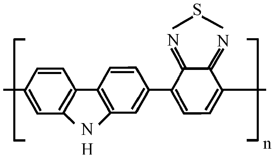
5 
6 
7 - Electrodes of the disclosed capacitor may be made of any suitable material, including but not limited to Pt, Cu, Al, Ag or Au.
- The capacitor is produced by a manufacturing method, which comprise the steps of a) preparation of a conducting substrate serving as one of the electrodes, b) application of a molecular material on the substrate, c) formation of the solid layer molecular material layer on the substrate, and d) formation of the second electrode on the solid molecular material layer, wherein the molecular material is described by the general formula
Dp-(Core)-Hq. (I)
whereCore 10 is a polarizable conductive anisometric core, having conjugated π-systems and characterized by a longitudinal axis, D and H are insulating substituents, and p and q are numbers of substituents D and H accordingly. The insulating substituents are attached to the polarizable anisometric core in apex positions, and p and q are independently selected fromvalues Core 10 is polyaniline (PANI), or a polarizable anisometric core forming molecular stacks due to π- π-interaction, or an electroconductive oligomer forming molecular stacks due to π- π-interaction, said polarizable anisometric core and said electroconductive oligomer being selected from the list comprising structural formulas corresponding to one ofstructures 2 to 7 as given in Table 1 above. - In the disclosed method at least one of the insulating groups D and at least one of the insulating groups H are independently selected from the list comprising alkyl, fluorinated alkyl, chlorinated alkyl, branched and complex alkyl, branched and complex fluorinated alkyl, branched and complex chlorinated alkyl groups, and any combination thereof. When the
Core 10 is polyaniline (PANI), the insulatingsubstituents 11 are fluorinated alkyl substituents - In one embodiment of the disclosed method the application step b) comprises application of a solution of the molecular material, and the solid layer formation step c) comprises drying to form a solid molecular material layer.
- In yet another embodiment of the disclosed method the application step b) comprises application of a melt of the molecular material, and the solid layer formation step c) comprises cooling down to form a solid molecular material layer.
- In order that the embodiments of the invention may be more readily understood, reference is made to the following example, which is intended to be illustrative of the invention, but is not intended to be limiting in scope.
- Example 1 describes a capacitor comprising a dielectric layer formed with the solid molecular material of lamellar structure as shown in
Figure 5 . - The capacitor comprises two
electrodes dielectric layer 15 which comprises the conductiveanisometric stacks 12 formed with the polarizable anisometric cores, and isotropic insulatingsublayers 16. Polyaniline (PANI) is used as the polarizable anisometric core, and fluorinated alkyl substituents are used as the insulating substituents. The conductive anisometric stacks formed with polyaniline (PANI) have the dielectric permittivity εcor equal to 10,000. Thickness of each insulating sublayers formed by the substituents is approximately dins=2 nm, and number of the insulating sublayers nins is equal to 500.Electrodes
Claims (12)
- A capacitor comprising
a first electrode (13),
a second electrode (14), and
a dielectric layer (15) of molecular material disposed between said first and second electrodes (13, 14),
wherein said electrodes (13, 14) are flat and planar and positioned parallel to each other, and
the molecular material is described by the general formula
Dp-(Core)-Hq (I)
where Core (10) is:- a polarizable conductive anisometric core forming molecular stacks (12) due to π- π-interaction selected from the group consisting of the following structural formulas 2, 5, 6 and 7:
2 
5 
6 
7 - an electroconductive oligomer (10) forming molecular stacks (12) due to π-π-interaction selected from the group consisting of the following structural formulas 3 and 4:
3 
4 - polyaniline (PANI), and
said Core (10) being characterized by a longitudinal axisD and H are insulating substituents (11) respectively attached at the opposite ends of the core molecule (10) according to said longitudinal axis, andp and q are numbers of the D and H substituents (11) accordingly,wherein said substituents (11) are attached to the Core (10) in apex positions, and p and q are independently selected from values 1, 2, 3, 4, and 5, and
wherein at least one of the insulating groups D (11) and at least one of the insulating groups H (11) is each selected independently from the group consisting of alkyl, fluorinated alkyl, chlorinated alkyl, branched alkyl, branched fluorinated alkyl, branched chlorinated alkyl groups, and any combination thereof, and
wherein when said Core (10) is polyaniline (PANI), the insulating substituents (11) are fluorinated alkyl substituents. - A capacitor according to Claim 1, wherein the anisometric cores (10) form conductive stacks (12) due to π- π-interaction, and the insulating substituents (11) form the insulating sublayers (16) surrounding said stacks, wherein a twist angle α is formed between the longitudinal axes of the adjacent anisometric cores (10), said twist angle is in the range of 0° ≤ α ≤ 90°, and distance between the cores in the stacks is 0.34±0.1nm.
- A capacitor according to Claim 2, wherein the anisometric cores (10) form the twisted conductive stacks (12), wherein said twist angle is in the range of 0° < α ≤ 90°.
- A capacitor according to Claim 3, wherein the dielectric layer (15) of molecular material has a hexagonal crystal structure.
- A capacitor according to Claim 2, wherein the anisometric cores (10) form the conductive stacks (12), wherein said twist angle α equals zero, and the longitudinal axes of the anisometric cores (10) are perpendicular to the electrodes (13, 14).
- A capacitor according to Claim 5, wherein the dielectric layer (15) of molecular material has a lamellar crystal structure.
- A capacitor according to Claim 6, wherein said polarizable anisometric cores (10) possess translational periodicity and symmetry at least in one direction.
- A capacitor according to Claim 1, wherein the electrodes (13, 14) are made of Pt, Cu, Al, Ag or Au.
- A capacitor according to Claim 1, comprising two electrodes (13, 14) made of copper, polyaniline (PANI) as the polarizable anisometric core (10), and fluorinated alkyl substituents as the insulating substituents (11).
- A method of producing a capacitor, which comprises the steps ofa) preparation of a conducting substrate serving as one of the electrodes (13, 14),b) application of a molecular material on the substrate,c) formation of the solid layer of the molecular material, andd) formation of the second electrode (13, 14) on the solid molecular material layer,
wherein the molecular material is described by the general formula
Dp-(Core)-Hq (I)
where Core (10) is:- a polarizable conductive anisometric core (10) forming molecular stacks (12) due to π- π-interaction selected from the group consisting of the following structural formulas 2, 5, 6 and 7:
2 
5 
6 
7 - an electroconductive oligomer (10) forming molecular stacks (12) due to π-π-interaction selected from the group consisting of the following structural formulas 3 and 4: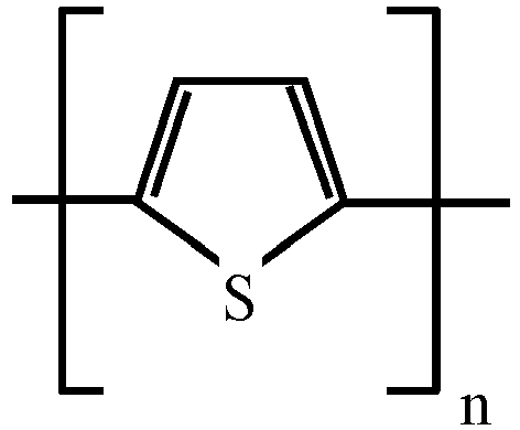
3 
4 - polyaniline (PANI), andsaid Core (10) being characterized by a longitudinal axis,D and H are insulating substituents (11) respectively attached at the opposite ends of the core molecule according to said longitudinal axis, andp and q are numbers of the D and H substituents (11) accordingly,wherein said substituents (11) are attached to the Core (10) in apex positions, and p and q are independently selected from values 1, 2, 3, 4, and 5, and wherein at least one of the insulating groups D (11) and at least one of the insulating groups H (11) is each selected independently from the group consisting of alkyl, fluorinated alkyl, chlorinated alkyl, branched alkyl, branched fluorinated alkyl, branched chlorinated alkyl groups, and any combination thereof, and
wherein when said Core (10) is polyaniline (PANI), the insulating substituents (11) are fluorinated alkyl substituents. - A method according to Claim 10, wherein the application step b) comprises application of a solution of the molecular material, and the solid layer formation step c) comprises drying to form a solid molecular material layer.
- A method according to Claim 10, wherein the application step b) comprises application of a melt of the molecular material, and the solid layer formation step c) comprises cooling down to form a solid molecular material layer.
Applications Claiming Priority (2)
| Application Number | Priority Date | Filing Date | Title |
|---|---|---|---|
| US201461991871P | 2014-05-12 | 2014-05-12 | |
| PCT/US2015/030356 WO2015175522A1 (en) | 2014-05-12 | 2015-05-12 | Capacitor and method of production thereof |
Publications (3)
| Publication Number | Publication Date |
|---|---|
| EP3143651A1 EP3143651A1 (en) | 2017-03-22 |
| EP3143651A4 EP3143651A4 (en) | 2017-12-13 |
| EP3143651B1 true EP3143651B1 (en) | 2020-09-16 |
Family
ID=54480548
Family Applications (1)
| Application Number | Title | Priority Date | Filing Date |
|---|---|---|---|
| EP15792405.1A Not-in-force EP3143651B1 (en) | 2014-05-12 | 2015-05-12 | Capacitor and method of production thereof |
Country Status (14)
| Country | Link |
|---|---|
| US (1) | US9589727B2 (en) |
| EP (1) | EP3143651B1 (en) |
| JP (2) | JP2017520128A (en) |
| KR (1) | KR20170005821A (en) |
| CN (1) | CN106463618B (en) |
| AU (1) | AU2015259345B2 (en) |
| CA (1) | CA2948008A1 (en) |
| IL (1) | IL248829A0 (en) |
| MX (1) | MX2016014827A (en) |
| RU (1) | RU2016143559A (en) |
| SG (1) | SG11201609438UA (en) |
| TW (1) | TW201618139A (en) |
| WO (1) | WO2015175522A1 (en) |
| ZA (1) | ZA201608040B (en) |
Families Citing this family (28)
| Publication number | Priority date | Publication date | Assignee | Title |
|---|---|---|---|---|
| US10347423B2 (en) | 2014-05-12 | 2019-07-09 | Capacitor Sciences Incorporated | Solid multilayer structure as semiproduct for meta-capacitor |
| US10319523B2 (en) | 2014-05-12 | 2019-06-11 | Capacitor Sciences Incorporated | Yanli dielectric materials and capacitor thereof |
| KR102331588B1 (en) | 2014-05-12 | 2021-11-30 | 캐패시터 사이언시스 인코포레이티드 | Energy storage device and method of production thereof |
| US10340082B2 (en) | 2015-05-12 | 2019-07-02 | Capacitor Sciences Incorporated | Capacitor and method of production thereof |
| US20170301477A1 (en) * | 2016-04-04 | 2017-10-19 | Capacitor Sciences Incorporated | Electro-polarizable compound and capacitor |
| WO2016073522A1 (en) | 2014-11-04 | 2016-05-12 | Capacitor Sciences Incorporated | Energy storage devices and methods of production thereof |
| JP2018511167A (en) | 2015-02-26 | 2018-04-19 | キャパシタ サイエンシス インコーポレイテッド | Self-healing capacitor and manufacturing method thereof |
| US9932358B2 (en) | 2015-05-21 | 2018-04-03 | Capacitor Science Incorporated | Energy storage molecular material, crystal dielectric layer and capacitor |
| US9941051B2 (en) | 2015-06-26 | 2018-04-10 | Capactor Sciences Incorporated | Coiled capacitor |
| US10026553B2 (en) | 2015-10-21 | 2018-07-17 | Capacitor Sciences Incorporated | Organic compound, crystal dielectric layer and capacitor |
| DE102015224739A1 (en) * | 2015-12-09 | 2017-06-14 | Robert Bosch Gmbh | Method and device for triggering pedestrian protection devices and / or pedestrian warning devices |
| US20170236642A1 (en) * | 2016-02-12 | 2017-08-17 | Capacitor Sciences Incorporated | para-FURUTA POLYMER AND CAPACITOR |
| US20170236641A1 (en) * | 2016-02-12 | 2017-08-17 | Capacitor Sciences Incorporated | Furuta co-polymer and capacitor |
| US10636575B2 (en) | 2016-02-12 | 2020-04-28 | Capacitor Sciences Incorporated | Furuta and para-Furuta polymer formulations and capacitors |
| US20170233528A1 (en) * | 2016-02-12 | 2017-08-17 | Capacitor Sciences Incorporated | Sharp polymer and capacitor |
| US10305295B2 (en) | 2016-02-12 | 2019-05-28 | Capacitor Sciences Incorporated | Energy storage cell, capacitive energy storage module, and capacitive energy storage system |
| US11092142B2 (en) * | 2017-11-20 | 2021-08-17 | Capacitor Sciences Incorporated | Plasma electric propulsion device |
| US9978517B2 (en) * | 2016-04-04 | 2018-05-22 | Capacitor Sciences Incorporated | Electro-polarizable compound and capacitor |
| US20170283618A1 (en) * | 2016-04-04 | 2017-10-05 | Capacitor Sciences Incorporated | Non-linear dielectric materials and capacitor |
| US10153087B2 (en) * | 2016-04-04 | 2018-12-11 | Capacitor Sciences Incorporated | Electro-polarizable compound and capacitor |
| WO2018021328A1 (en) * | 2016-07-26 | 2018-02-01 | 日産化学工業株式会社 | Polymer composition |
| US10395841B2 (en) | 2016-12-02 | 2019-08-27 | Capacitor Sciences Incorporated | Multilayered electrode and film energy storage device |
| US10388461B2 (en) | 2017-08-02 | 2019-08-20 | Perriquest Defense Research Enterprises, Llc | Capacitor arrangements |
| US10163575B1 (en) | 2017-11-07 | 2018-12-25 | Capacitor Sciences Incorporated | Non-linear capacitor and energy storage device comprising thereof |
| JP2021503488A (en) * | 2017-11-20 | 2021-02-12 | キャパシター サイエンシズ インコーポレイテッドCapacitor Sciences Incorporated | Hein electron-polarizing compounds and their capacitors |
| US10403435B2 (en) | 2017-12-15 | 2019-09-03 | Capacitor Sciences Incorporated | Edder compound and capacitor thereof |
| US11476261B2 (en) * | 2019-02-27 | 2022-10-18 | Kepler Computing Inc. | High-density low voltage non-volatile memory with unidirectional plate-line and bit-line and pillar capacitor |
| JP7444561B2 (en) | 2019-08-08 | 2024-03-06 | 株式会社東芝 | Aluminum electrolytic capacitor, electrical equipment, and method for manufacturing aluminum electrolytic capacitor |
Family Cites Families (19)
| Publication number | Priority date | Publication date | Assignee | Title |
|---|---|---|---|---|
| US6501093B1 (en) | 1994-04-04 | 2002-12-31 | Alvin M. Marks | Quantum energy storage or retrieval device |
| US7033406B2 (en) | 2001-04-12 | 2006-04-25 | Eestor, Inc. | Electrical-energy-storage unit (EESU) utilizing ceramic and integrated-circuit technologies for replacement of electrochemical batteries |
| DE60212668T2 (en) * | 2001-09-27 | 2007-06-21 | 3M Innovative Properties Co., St. Paul | SEMICONDUCTOR BASED ON SUBSTITUTED PENTACEN |
| DE10248722A1 (en) | 2002-10-18 | 2004-05-06 | Infineon Technologies Ag | Integrated circuit arrangement with capacitor and manufacturing process |
| EP1592029B1 (en) * | 2003-02-07 | 2019-07-03 | Showa Denko K.K. | Production method for the capacitor |
| US7466536B1 (en) | 2004-08-13 | 2008-12-16 | Eestor, Inc. | Utilization of poly(ethylene terephthalate) plastic and composition-modified barium titanate powders in a matrix that allows polarization and the use of integrated-circuit technologies for the production of lightweight ultrahigh electrical energy storage units (EESU) |
| JP3841814B1 (en) * | 2005-04-28 | 2006-11-08 | 三井金属鉱業株式会社 | Capacitor layer forming material and method for manufacturing the capacitor layer forming material |
| US20090030152A1 (en) | 2005-12-28 | 2009-01-29 | Qiming Zhang | High Electric Energy Density Polymer Capacitors With Fast Discharge Speed and High Efficiency Based On Unique Poly (Vinylidene Fluoride) Copolymers and Terpolymers as Dielectric Materials |
| US20080002329A1 (en) * | 2006-07-02 | 2008-01-03 | Pohm Arthur V | High Dielectric, Non-Linear Capacitor |
| GB0616358D0 (en) * | 2006-08-16 | 2006-09-27 | Crysoptix Ltd | Anisotropic polymer film and method of production thereof |
| GB0622150D0 (en) * | 2006-11-06 | 2006-12-20 | Kontrakt Technology Ltd | Anisotropic semiconductor film and method of production thereof |
| MX2011007202A (en) | 2009-01-16 | 2011-07-28 | Univ The Board Of Trustees Of The Leland Stanford Junio R | ULTRACAPACITOR OF QUANTIC POINT AND ELECTRONIC BATTERY. |
| US8524398B2 (en) | 2009-04-01 | 2013-09-03 | The Board Of Trustees Of The Leland Stanford Junior University | All-electron battery having area-enhanced electrodes |
| KR20110122051A (en) * | 2010-05-03 | 2011-11-09 | 제일모직주식회사 | Compound for organic photoelectric device and organic photoelectric device comprising same |
| US20120008251A1 (en) * | 2010-07-12 | 2012-01-12 | Wei-Ching Yu | Film capacitors comprising melt-stretched films as dielectrics |
| JP5531163B2 (en) | 2011-07-05 | 2014-06-25 | 株式会社村田製作所 | Dielectric thin film, dielectric thin film element, and thin film capacitor |
| US9732194B2 (en) * | 2011-12-09 | 2017-08-15 | Nanyang Technological University | Graft copolymers of a poly(vinylidene fluoride)-based polymer and at least one type of electrically conductive polymer, and methods for forming the graft copolymers |
| US9087645B2 (en) | 2012-01-30 | 2015-07-21 | QuantrumScape Corporation | Solid state energy storage devices |
| US20130334657A1 (en) | 2012-06-15 | 2013-12-19 | Taiwan Semiconductor Manufacturing Co., Ltd. | Planar interdigitated capacitor structures and methods of forming the same |
-
2015
- 2015-05-12 US US14/710,491 patent/US9589727B2/en not_active Expired - Fee Related
- 2015-05-12 AU AU2015259345A patent/AU2015259345B2/en not_active Ceased
- 2015-05-12 MX MX2016014827A patent/MX2016014827A/en unknown
- 2015-05-12 KR KR1020167033251A patent/KR20170005821A/en not_active Ceased
- 2015-05-12 RU RU2016143559A patent/RU2016143559A/en not_active Application Discontinuation
- 2015-05-12 CN CN201580025110.6A patent/CN106463618B/en not_active Expired - Fee Related
- 2015-05-12 EP EP15792405.1A patent/EP3143651B1/en not_active Not-in-force
- 2015-05-12 SG SG11201609438UA patent/SG11201609438UA/en unknown
- 2015-05-12 CA CA2948008A patent/CA2948008A1/en not_active Abandoned
- 2015-05-12 JP JP2017512654A patent/JP2017520128A/en active Pending
- 2015-05-12 TW TW104115076A patent/TW201618139A/en unknown
- 2015-05-12 WO PCT/US2015/030356 patent/WO2015175522A1/en not_active Ceased
-
2016
- 2016-11-08 IL IL248829A patent/IL248829A0/en unknown
- 2016-11-21 ZA ZA2016/08040A patent/ZA201608040B/en unknown
-
2020
- 2020-04-24 JP JP2020077405A patent/JP2020120130A/en active Pending
Non-Patent Citations (1)
| Title |
|---|
| None * |
Also Published As
| Publication number | Publication date |
|---|---|
| US9589727B2 (en) | 2017-03-07 |
| EP3143651A4 (en) | 2017-12-13 |
| CN106463618A (en) | 2017-02-22 |
| CA2948008A1 (en) | 2015-11-19 |
| RU2016143559A (en) | 2018-06-19 |
| AU2015259345A1 (en) | 2016-11-24 |
| US20160020027A1 (en) | 2016-01-21 |
| ZA201608040B (en) | 2018-11-28 |
| SG11201609438UA (en) | 2016-12-29 |
| MX2016014827A (en) | 2017-03-10 |
| AU2015259345B2 (en) | 2018-03-01 |
| JP2020120130A (en) | 2020-08-06 |
| KR20170005821A (en) | 2017-01-16 |
| JP2017520128A (en) | 2017-07-20 |
| EP3143651A1 (en) | 2017-03-22 |
| TW201618139A (en) | 2016-05-16 |
| WO2015175522A1 (en) | 2015-11-19 |
| CN106463618B (en) | 2019-06-14 |
| IL248829A0 (en) | 2017-01-31 |
Similar Documents
| Publication | Publication Date | Title |
|---|---|---|
| EP3143651B1 (en) | Capacitor and method of production thereof | |
| EP3216037B1 (en) | Energy storage devices and methods of production thereof | |
| US10347424B2 (en) | Energy storage device and method of production thereof | |
| US10685782B2 (en) | Capacitor and method of production thereof | |
| WO2017139451A1 (en) | para-FURUTA POLYMER AND CAPACITOR |
Legal Events
| Date | Code | Title | Description |
|---|---|---|---|
| STAA | Information on the status of an ep patent application or granted ep patent |
Free format text: STATUS: THE INTERNATIONAL PUBLICATION HAS BEEN MADE |
|
| PUAI | Public reference made under article 153(3) epc to a published international application that has entered the european phase |
Free format text: ORIGINAL CODE: 0009012 |
|
| STAA | Information on the status of an ep patent application or granted ep patent |
Free format text: STATUS: REQUEST FOR EXAMINATION WAS MADE |
|
| 17P | Request for examination filed |
Effective date: 20161121 |
|
| AK | Designated contracting states |
Kind code of ref document: A1 Designated state(s): AL AT BE BG CH CY CZ DE DK EE ES FI FR GB GR HR HU IE IS IT LI LT LU LV MC MK MT NL NO PL PT RO RS SE SI SK SM TR |
|
| AX | Request for extension of the european patent |
Extension state: BA ME |
|
| DAV | Request for validation of the european patent (deleted) | ||
| DAX | Request for extension of the european patent (deleted) | ||
| A4 | Supplementary search report drawn up and despatched |
Effective date: 20171110 |
|
| RIC1 | Information provided on ipc code assigned before grant |
Ipc: H01G 4/14 20060101AFI20171106BHEP Ipc: H01L 49/02 20060101ALI20171106BHEP |
|
| STAA | Information on the status of an ep patent application or granted ep patent |
Free format text: STATUS: EXAMINATION IS IN PROGRESS |
|
| 17Q | First examination report despatched |
Effective date: 20180716 |
|
| REG | Reference to a national code |
Ref country code: DE Ref legal event code: R079 Ref document number: 602015059219 Country of ref document: DE Free format text: PREVIOUS MAIN CLASS: H01L0049020000 Ipc: H01G0004140000 |
|
| RIC1 | Information provided on ipc code assigned before grant |
Ipc: H01G 4/14 20060101AFI20200113BHEP |
|
| GRAP | Despatch of communication of intention to grant a patent |
Free format text: ORIGINAL CODE: EPIDOSNIGR1 |
|
| STAA | Information on the status of an ep patent application or granted ep patent |
Free format text: STATUS: GRANT OF PATENT IS INTENDED |
|
| INTG | Intention to grant announced |
Effective date: 20200326 |
|
| GRAJ | Information related to disapproval of communication of intention to grant by the applicant or resumption of examination proceedings by the epo deleted |
Free format text: ORIGINAL CODE: EPIDOSDIGR1 |
|
| STAA | Information on the status of an ep patent application or granted ep patent |
Free format text: STATUS: EXAMINATION IS IN PROGRESS |
|
| GRAR | Information related to intention to grant a patent recorded |
Free format text: ORIGINAL CODE: EPIDOSNIGR71 |
|
| GRAS | Grant fee paid |
Free format text: ORIGINAL CODE: EPIDOSNIGR3 |
|
| STAA | Information on the status of an ep patent application or granted ep patent |
Free format text: STATUS: GRANT OF PATENT IS INTENDED |
|
| GRAA | (expected) grant |
Free format text: ORIGINAL CODE: 0009210 |
|
| STAA | Information on the status of an ep patent application or granted ep patent |
Free format text: STATUS: THE PATENT HAS BEEN GRANTED |
|
| INTC | Intention to grant announced (deleted) | ||
| AK | Designated contracting states |
Kind code of ref document: B1 Designated state(s): AL AT BE BG CH CY CZ DE DK EE ES FI FR GB GR HR HU IE IS IT LI LT LU LV MC MK MT NL NO PL PT RO RS SE SI SK SM TR |
|
| INTG | Intention to grant announced |
Effective date: 20200807 |
|
| REG | Reference to a national code |
Ref country code: GB Ref legal event code: FG4D |
|
| REG | Reference to a national code |
Ref country code: CH Ref legal event code: EP |
|
| REG | Reference to a national code |
Ref country code: DE Ref legal event code: R096 Ref document number: 602015059219 Country of ref document: DE |
|
| REG | Reference to a national code |
Ref country code: IE Ref legal event code: FG4D |
|
| REG | Reference to a national code |
Ref country code: AT Ref legal event code: REF Ref document number: 1314899 Country of ref document: AT Kind code of ref document: T Effective date: 20201015 |
|
| PG25 | Lapsed in a contracting state [announced via postgrant information from national office to epo] |
Ref country code: SE Free format text: LAPSE BECAUSE OF FAILURE TO SUBMIT A TRANSLATION OF THE DESCRIPTION OR TO PAY THE FEE WITHIN THE PRESCRIBED TIME-LIMIT Effective date: 20200916 Ref country code: BG Free format text: LAPSE BECAUSE OF FAILURE TO SUBMIT A TRANSLATION OF THE DESCRIPTION OR TO PAY THE FEE WITHIN THE PRESCRIBED TIME-LIMIT Effective date: 20201216 Ref country code: HR Free format text: LAPSE BECAUSE OF FAILURE TO SUBMIT A TRANSLATION OF THE DESCRIPTION OR TO PAY THE FEE WITHIN THE PRESCRIBED TIME-LIMIT Effective date: 20200916 Ref country code: NO Free format text: LAPSE BECAUSE OF FAILURE TO SUBMIT A TRANSLATION OF THE DESCRIPTION OR TO PAY THE FEE WITHIN THE PRESCRIBED TIME-LIMIT Effective date: 20201216 Ref country code: GR Free format text: LAPSE BECAUSE OF FAILURE TO SUBMIT A TRANSLATION OF THE DESCRIPTION OR TO PAY THE FEE WITHIN THE PRESCRIBED TIME-LIMIT Effective date: 20201217 Ref country code: FI Free format text: LAPSE BECAUSE OF FAILURE TO SUBMIT A TRANSLATION OF THE DESCRIPTION OR TO PAY THE FEE WITHIN THE PRESCRIBED TIME-LIMIT Effective date: 20200916 |
|
| REG | Reference to a national code |
Ref country code: AT Ref legal event code: MK05 Ref document number: 1314899 Country of ref document: AT Kind code of ref document: T Effective date: 20200916 |
|
| REG | Reference to a national code |
Ref country code: NL Ref legal event code: MP Effective date: 20200916 |
|
| PG25 | Lapsed in a contracting state [announced via postgrant information from national office to epo] |
Ref country code: LV Free format text: LAPSE BECAUSE OF FAILURE TO SUBMIT A TRANSLATION OF THE DESCRIPTION OR TO PAY THE FEE WITHIN THE PRESCRIBED TIME-LIMIT Effective date: 20200916 Ref country code: RS Free format text: LAPSE BECAUSE OF FAILURE TO SUBMIT A TRANSLATION OF THE DESCRIPTION OR TO PAY THE FEE WITHIN THE PRESCRIBED TIME-LIMIT Effective date: 20200916 |
|
| REG | Reference to a national code |
Ref country code: LT Ref legal event code: MG4D |
|
| PG25 | Lapsed in a contracting state [announced via postgrant information from national office to epo] |
Ref country code: CZ Free format text: LAPSE BECAUSE OF FAILURE TO SUBMIT A TRANSLATION OF THE DESCRIPTION OR TO PAY THE FEE WITHIN THE PRESCRIBED TIME-LIMIT Effective date: 20200916 Ref country code: NL Free format text: LAPSE BECAUSE OF FAILURE TO SUBMIT A TRANSLATION OF THE DESCRIPTION OR TO PAY THE FEE WITHIN THE PRESCRIBED TIME-LIMIT Effective date: 20200916 Ref country code: LT Free format text: LAPSE BECAUSE OF FAILURE TO SUBMIT A TRANSLATION OF THE DESCRIPTION OR TO PAY THE FEE WITHIN THE PRESCRIBED TIME-LIMIT Effective date: 20200916 Ref country code: SM Free format text: LAPSE BECAUSE OF FAILURE TO SUBMIT A TRANSLATION OF THE DESCRIPTION OR TO PAY THE FEE WITHIN THE PRESCRIBED TIME-LIMIT Effective date: 20200916 Ref country code: RO Free format text: LAPSE BECAUSE OF FAILURE TO SUBMIT A TRANSLATION OF THE DESCRIPTION OR TO PAY THE FEE WITHIN THE PRESCRIBED TIME-LIMIT Effective date: 20200916 Ref country code: PT Free format text: LAPSE BECAUSE OF FAILURE TO SUBMIT A TRANSLATION OF THE DESCRIPTION OR TO PAY THE FEE WITHIN THE PRESCRIBED TIME-LIMIT Effective date: 20210118 Ref country code: EE Free format text: LAPSE BECAUSE OF FAILURE TO SUBMIT A TRANSLATION OF THE DESCRIPTION OR TO PAY THE FEE WITHIN THE PRESCRIBED TIME-LIMIT Effective date: 20200916 |
|
| PG25 | Lapsed in a contracting state [announced via postgrant information from national office to epo] |
Ref country code: AT Free format text: LAPSE BECAUSE OF FAILURE TO SUBMIT A TRANSLATION OF THE DESCRIPTION OR TO PAY THE FEE WITHIN THE PRESCRIBED TIME-LIMIT Effective date: 20200916 Ref country code: AL Free format text: LAPSE BECAUSE OF FAILURE TO SUBMIT A TRANSLATION OF THE DESCRIPTION OR TO PAY THE FEE WITHIN THE PRESCRIBED TIME-LIMIT Effective date: 20200916 Ref country code: ES Free format text: LAPSE BECAUSE OF FAILURE TO SUBMIT A TRANSLATION OF THE DESCRIPTION OR TO PAY THE FEE WITHIN THE PRESCRIBED TIME-LIMIT Effective date: 20200916 Ref country code: IS Free format text: LAPSE BECAUSE OF FAILURE TO SUBMIT A TRANSLATION OF THE DESCRIPTION OR TO PAY THE FEE WITHIN THE PRESCRIBED TIME-LIMIT Effective date: 20210116 Ref country code: PL Free format text: LAPSE BECAUSE OF FAILURE TO SUBMIT A TRANSLATION OF THE DESCRIPTION OR TO PAY THE FEE WITHIN THE PRESCRIBED TIME-LIMIT Effective date: 20200916 |
|
| REG | Reference to a national code |
Ref country code: DE Ref legal event code: R097 Ref document number: 602015059219 Country of ref document: DE |
|
| PG25 | Lapsed in a contracting state [announced via postgrant information from national office to epo] |
Ref country code: SK Free format text: LAPSE BECAUSE OF FAILURE TO SUBMIT A TRANSLATION OF THE DESCRIPTION OR TO PAY THE FEE WITHIN THE PRESCRIBED TIME-LIMIT Effective date: 20200916 |
|
| PLBE | No opposition filed within time limit |
Free format text: ORIGINAL CODE: 0009261 |
|
| STAA | Information on the status of an ep patent application or granted ep patent |
Free format text: STATUS: NO OPPOSITION FILED WITHIN TIME LIMIT |
|
| 26N | No opposition filed |
Effective date: 20210617 |
|
| PG25 | Lapsed in a contracting state [announced via postgrant information from national office to epo] |
Ref country code: SI Free format text: LAPSE BECAUSE OF FAILURE TO SUBMIT A TRANSLATION OF THE DESCRIPTION OR TO PAY THE FEE WITHIN THE PRESCRIBED TIME-LIMIT Effective date: 20200916 Ref country code: DK Free format text: LAPSE BECAUSE OF FAILURE TO SUBMIT A TRANSLATION OF THE DESCRIPTION OR TO PAY THE FEE WITHIN THE PRESCRIBED TIME-LIMIT Effective date: 20200916 |
|
| PG25 | Lapsed in a contracting state [announced via postgrant information from national office to epo] |
Ref country code: IT Free format text: LAPSE BECAUSE OF FAILURE TO SUBMIT A TRANSLATION OF THE DESCRIPTION OR TO PAY THE FEE WITHIN THE PRESCRIBED TIME-LIMIT Effective date: 20200916 |
|
| REG | Reference to a national code |
Ref country code: CH Ref legal event code: PL |
|
| PG25 | Lapsed in a contracting state [announced via postgrant information from national office to epo] |
Ref country code: CH Free format text: LAPSE BECAUSE OF NON-PAYMENT OF DUE FEES Effective date: 20210531 Ref country code: MC Free format text: LAPSE BECAUSE OF FAILURE TO SUBMIT A TRANSLATION OF THE DESCRIPTION OR TO PAY THE FEE WITHIN THE PRESCRIBED TIME-LIMIT Effective date: 20200916 Ref country code: LI Free format text: LAPSE BECAUSE OF NON-PAYMENT OF DUE FEES Effective date: 20210531 Ref country code: LU Free format text: LAPSE BECAUSE OF NON-PAYMENT OF DUE FEES Effective date: 20210512 |
|
| REG | Reference to a national code |
Ref country code: BE Ref legal event code: MM Effective date: 20210531 |
|
| PG25 | Lapsed in a contracting state [announced via postgrant information from national office to epo] |
Ref country code: IE Free format text: LAPSE BECAUSE OF NON-PAYMENT OF DUE FEES Effective date: 20210512 |
|
| PG25 | Lapsed in a contracting state [announced via postgrant information from national office to epo] |
Ref country code: BE Free format text: LAPSE BECAUSE OF NON-PAYMENT OF DUE FEES Effective date: 20210531 |
|
| PG25 | Lapsed in a contracting state [announced via postgrant information from national office to epo] |
Ref country code: HU Free format text: LAPSE BECAUSE OF FAILURE TO SUBMIT A TRANSLATION OF THE DESCRIPTION OR TO PAY THE FEE WITHIN THE PRESCRIBED TIME-LIMIT; INVALID AB INITIO Effective date: 20150512 |
|
| PG25 | Lapsed in a contracting state [announced via postgrant information from national office to epo] |
Ref country code: CY Free format text: LAPSE BECAUSE OF FAILURE TO SUBMIT A TRANSLATION OF THE DESCRIPTION OR TO PAY THE FEE WITHIN THE PRESCRIBED TIME-LIMIT Effective date: 20200916 |
|
| PGFP | Annual fee paid to national office [announced via postgrant information from national office to epo] |
Ref country code: FR Payment date: 20230420 Year of fee payment: 9 Ref country code: DE Payment date: 20230419 Year of fee payment: 9 |
|
| PGFP | Annual fee paid to national office [announced via postgrant information from national office to epo] |
Ref country code: GB Payment date: 20230420 Year of fee payment: 9 |
|
| PG25 | Lapsed in a contracting state [announced via postgrant information from national office to epo] |
Ref country code: MK Free format text: LAPSE BECAUSE OF FAILURE TO SUBMIT A TRANSLATION OF THE DESCRIPTION OR TO PAY THE FEE WITHIN THE PRESCRIBED TIME-LIMIT Effective date: 20200916 |
|
| PG25 | Lapsed in a contracting state [announced via postgrant information from national office to epo] |
Ref country code: TR Free format text: LAPSE BECAUSE OF FAILURE TO SUBMIT A TRANSLATION OF THE DESCRIPTION OR TO PAY THE FEE WITHIN THE PRESCRIBED TIME-LIMIT Effective date: 20200916 |
|
| PG25 | Lapsed in a contracting state [announced via postgrant information from national office to epo] |
Ref country code: MT Free format text: LAPSE BECAUSE OF FAILURE TO SUBMIT A TRANSLATION OF THE DESCRIPTION OR TO PAY THE FEE WITHIN THE PRESCRIBED TIME-LIMIT Effective date: 20200916 |
|
| REG | Reference to a national code |
Ref country code: DE Ref legal event code: R119 Ref document number: 602015059219 Country of ref document: DE |
|
| GBPC | Gb: european patent ceased through non-payment of renewal fee |
Effective date: 20240512 |
|
| PG25 | Lapsed in a contracting state [announced via postgrant information from national office to epo] |
Ref country code: DE Free format text: LAPSE BECAUSE OF NON-PAYMENT OF DUE FEES Effective date: 20241203 |
|
| PG25 | Lapsed in a contracting state [announced via postgrant information from national office to epo] |
Ref country code: FR Free format text: LAPSE BECAUSE OF NON-PAYMENT OF DUE FEES Effective date: 20240531 |
|
| PG25 | Lapsed in a contracting state [announced via postgrant information from national office to epo] |
Ref country code: GB Free format text: LAPSE BECAUSE OF NON-PAYMENT OF DUE FEES Effective date: 20240512 |