EP3096186A3 - Lithography exposure device for lithographic exposure with single or multi-level laser projection units with one or more wavelengths - Google Patents
Lithography exposure device for lithographic exposure with single or multi-level laser projection units with one or more wavelengths Download PDFInfo
- Publication number
- EP3096186A3 EP3096186A3 EP16161954.9A EP16161954A EP3096186A3 EP 3096186 A3 EP3096186 A3 EP 3096186A3 EP 16161954 A EP16161954 A EP 16161954A EP 3096186 A3 EP3096186 A3 EP 3096186A3
- Authority
- EP
- European Patent Office
- Prior art keywords
- exposure device
- exposure
- wavelengths
- lithographic
- lithography
- Prior art date
- Legal status (The legal status is an assumption and is not a legal conclusion. Google has not performed a legal analysis and makes no representation as to the accuracy of the status listed.)
- Withdrawn
Links
Classifications
-
- G—PHYSICS
- G03—PHOTOGRAPHY; CINEMATOGRAPHY; ANALOGOUS TECHNIQUES USING WAVES OTHER THAN OPTICAL WAVES; ELECTROGRAPHY; HOLOGRAPHY
- G03F—PHOTOMECHANICAL PRODUCTION OF TEXTURED OR PATTERNED SURFACES, e.g. FOR PRINTING, FOR PROCESSING OF SEMICONDUCTOR DEVICES; MATERIALS THEREFOR; ORIGINALS THEREFOR; APPARATUS SPECIALLY ADAPTED THEREFOR
- G03F7/00—Photomechanical, e.g. photolithographic, production of textured or patterned surfaces, e.g. printing surfaces; Materials therefor, e.g. comprising photoresists; Apparatus specially adapted therefor
- G03F7/70—Microphotolithographic exposure; Apparatus therefor
- G03F7/70383—Direct write, i.e. pattern is written directly without the use of a mask by one or multiple beams
- G03F7/70391—Addressable array sources specially adapted to produce patterns, e.g. addressable LED arrays
-
- G—PHYSICS
- G03—PHOTOGRAPHY; CINEMATOGRAPHY; ANALOGOUS TECHNIQUES USING WAVES OTHER THAN OPTICAL WAVES; ELECTROGRAPHY; HOLOGRAPHY
- G03F—PHOTOMECHANICAL PRODUCTION OF TEXTURED OR PATTERNED SURFACES, e.g. FOR PRINTING, FOR PROCESSING OF SEMICONDUCTOR DEVICES; MATERIALS THEREFOR; ORIGINALS THEREFOR; APPARATUS SPECIALLY ADAPTED THEREFOR
- G03F7/00—Photomechanical, e.g. photolithographic, production of textured or patterned surfaces, e.g. printing surfaces; Materials therefor, e.g. comprising photoresists; Apparatus specially adapted therefor
- G03F7/70—Microphotolithographic exposure; Apparatus therefor
- G03F7/70383—Direct write, i.e. pattern is written directly without the use of a mask by one or multiple beams
-
- G—PHYSICS
- G03—PHOTOGRAPHY; CINEMATOGRAPHY; ANALOGOUS TECHNIQUES USING WAVES OTHER THAN OPTICAL WAVES; ELECTROGRAPHY; HOLOGRAPHY
- G03F—PHOTOMECHANICAL PRODUCTION OF TEXTURED OR PATTERNED SURFACES, e.g. FOR PRINTING, FOR PROCESSING OF SEMICONDUCTOR DEVICES; MATERIALS THEREFOR; ORIGINALS THEREFOR; APPARATUS SPECIALLY ADAPTED THEREFOR
- G03F7/00—Photomechanical, e.g. photolithographic, production of textured or patterned surfaces, e.g. printing surfaces; Materials therefor, e.g. comprising photoresists; Apparatus specially adapted therefor
- G03F7/70—Microphotolithographic exposure; Apparatus therefor
- G03F7/70691—Handling of masks or workpieces
- G03F7/70791—Large workpieces, e.g. glass substrates for flat panel displays or solar panels
-
- H—ELECTRICITY
- H05—ELECTRIC TECHNIQUES NOT OTHERWISE PROVIDED FOR
- H05K—PRINTED CIRCUITS; CASINGS OR CONSTRUCTIONAL DETAILS OF ELECTRIC APPARATUS; MANUFACTURE OF ASSEMBLAGES OF ELECTRICAL COMPONENTS
- H05K2203/00—Indexing scheme relating to apparatus or processes for manufacturing printed circuits covered by H05K3/00
- H05K2203/10—Using electric, magnetic and electromagnetic fields; Using laser light
- H05K2203/107—Using laser light
- H05K2203/108—Using a plurality of lasers or laser light with a plurality of wavelengths
-
- H—ELECTRICITY
- H05—ELECTRIC TECHNIQUES NOT OTHERWISE PROVIDED FOR
- H05K—PRINTED CIRCUITS; CASINGS OR CONSTRUCTIONAL DETAILS OF ELECTRIC APPARATUS; MANUFACTURE OF ASSEMBLAGES OF ELECTRICAL COMPONENTS
- H05K3/00—Apparatus or processes for manufacturing printed circuits
- H05K3/0073—Masks not provided for in groups H05K3/02 - H05K3/46, e.g. for photomechanical production of patterned surfaces
- H05K3/0082—Masks not provided for in groups H05K3/02 - H05K3/46, e.g. for photomechanical production of patterned surfaces characterised by the exposure method of radiation-sensitive masks
-
- H—ELECTRICITY
- H05—ELECTRIC TECHNIQUES NOT OTHERWISE PROVIDED FOR
- H05K—PRINTED CIRCUITS; CASINGS OR CONSTRUCTIONAL DETAILS OF ELECTRIC APPARATUS; MANUFACTURE OF ASSEMBLAGES OF ELECTRICAL COMPONENTS
- H05K3/00—Apparatus or processes for manufacturing printed circuits
- H05K3/02—Apparatus or processes for manufacturing printed circuits in which the conductive material is applied to the surface of the insulating support and is thereafter removed from such areas of the surface which are not intended for current conducting or shielding
- H05K3/06—Apparatus or processes for manufacturing printed circuits in which the conductive material is applied to the surface of the insulating support and is thereafter removed from such areas of the surface which are not intended for current conducting or shielding the conductive material being removed chemically or electrolytically, e.g. by photo-etch process
- H05K3/061—Etching masks
- H05K3/064—Photoresists
-
- H—ELECTRICITY
- H05—ELECTRIC TECHNIQUES NOT OTHERWISE PROVIDED FOR
- H05K—PRINTED CIRCUITS; CASINGS OR CONSTRUCTIONAL DETAILS OF ELECTRIC APPARATUS; MANUFACTURE OF ASSEMBLAGES OF ELECTRICAL COMPONENTS
- H05K3/00—Apparatus or processes for manufacturing printed circuits
- H05K3/22—Secondary treatment of printed circuits
- H05K3/28—Applying non-metallic protective coatings
Landscapes
- Physics & Mathematics (AREA)
- General Physics & Mathematics (AREA)
- Life Sciences & Earth Sciences (AREA)
- Sustainable Development (AREA)
- Exposure And Positioning Against Photoresist Photosensitive Materials (AREA)
Abstract
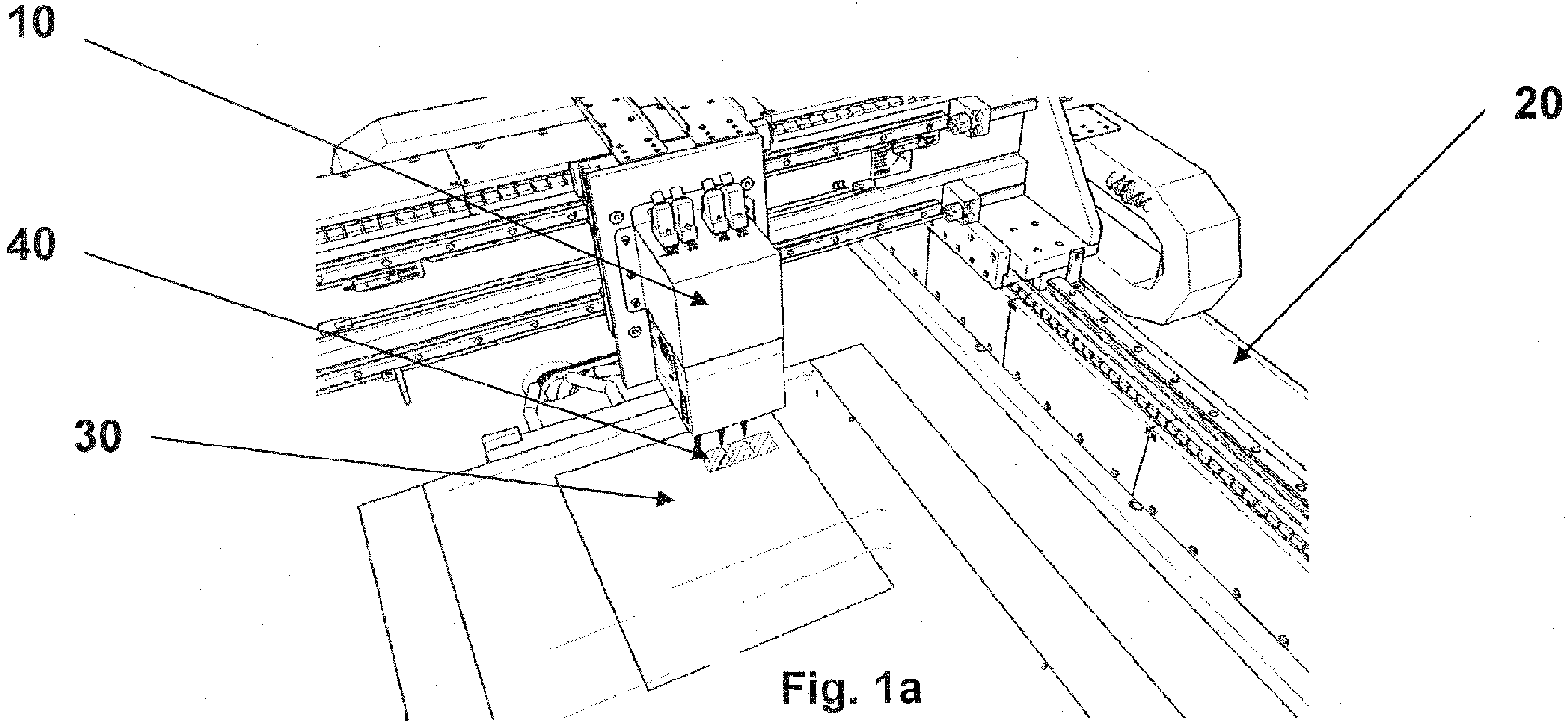
Die Erfindung betrifft eine Lithografiebelichtungseinrichtung zur lithographischen direkten Belichten eines Musters auf einem Substrat (30), das eine lichtempfindliche Schicht im UV Bereich von 350 nm - 450 nm aufweist, sowie ein entsprechendes Verfahren. Die Lithografiebelichtungseinrichtung umfasst eine Belichtungseinrichtung (10) die eine modulierte Lichtquelle mit einer oder mehreren UV-Laserlichtquellen (11) aufweist, zur Erzeugung eines kollimierten UV-Laserlichts (13) im Wellenlängenbereich von 350 nm - 450 nm. Zudem weist die Lithografiebelichtungseinrichtung eine veränderbare Ablenkeinrichtung (12) auf, mit der das kollimierte UV-Laserlicht (13) abgelenkt wir, um das Muster auf das Substrat (30) zu Belichten.
Applications Claiming Priority (2)
| Application Number | Priority Date | Filing Date | Title |
|---|---|---|---|
| DE102013018773 | 2013-11-08 | ||
| EP14192305.2A EP2871525A3 (en) | 2013-11-08 | 2014-11-07 | Lithography exposure device for lithographic exposure with single or multi-level laser project units with one or more wavelengths |
Related Parent Applications (1)
| Application Number | Title | Priority Date | Filing Date |
|---|---|---|---|
| EP14192305.2A Division EP2871525A3 (en) | 2013-11-08 | 2014-11-07 | Lithography exposure device for lithographic exposure with single or multi-level laser project units with one or more wavelengths |
Publications (2)
| Publication Number | Publication Date |
|---|---|
| EP3096186A2 EP3096186A2 (en) | 2016-11-23 |
| EP3096186A3 true EP3096186A3 (en) | 2017-04-12 |
Family
ID=51866079
Family Applications (2)
| Application Number | Title | Priority Date | Filing Date |
|---|---|---|---|
| EP16161954.9A Withdrawn EP3096186A3 (en) | 2013-11-08 | 2014-11-07 | Lithography exposure device for lithographic exposure with single or multi-level laser projection units with one or more wavelengths |
| EP14192305.2A Withdrawn EP2871525A3 (en) | 2013-11-08 | 2014-11-07 | Lithography exposure device for lithographic exposure with single or multi-level laser project units with one or more wavelengths |
Family Applications After (1)
| Application Number | Title | Priority Date | Filing Date |
|---|---|---|---|
| EP14192305.2A Withdrawn EP2871525A3 (en) | 2013-11-08 | 2014-11-07 | Lithography exposure device for lithographic exposure with single or multi-level laser project units with one or more wavelengths |
Country Status (1)
| Country | Link |
|---|---|
| EP (2) | EP3096186A3 (en) |
Families Citing this family (4)
| Publication number | Priority date | Publication date | Assignee | Title |
|---|---|---|---|---|
| EP3197249B1 (en) | 2016-01-20 | 2022-09-21 | Limata GmbH | Direct exposure device for direct exposure of soldering stop layers in two-dimensional environment with short-term tempering |
| DE102017103624A1 (en) * | 2017-02-22 | 2018-08-23 | Manz Ag | exposure system |
| CN113597132B (en) * | 2021-09-06 | 2022-08-02 | 深圳市先地图像科技有限公司 | Device and method for controlling laser power according to photosensitive ink of solder mask layer of PCB (printed circuit board) |
| CN115209637A (en) * | 2022-07-28 | 2022-10-18 | 江西旭昇电子有限公司 | Thick copper plate solder mask manufacturing method |
Citations (8)
| Publication number | Priority date | Publication date | Assignee | Title |
|---|---|---|---|---|
| US20020141024A1 (en) * | 2001-01-04 | 2002-10-03 | Wolfgang Retschke | Direct pattern writer |
| US20050002005A1 (en) * | 2003-07-03 | 2005-01-06 | Fuji Photo Film Co., Ltd. | Image forming apparatus |
| US20060215143A1 (en) * | 2005-03-22 | 2006-09-28 | Yoshihide Yamaguchi | Exposure apparatus and exposing method and method of manufacturing a printed wiring board |
| DE102006006797A1 (en) * | 2005-03-24 | 2006-09-28 | Hitachi Via Mechanics, Ltd., Ebina | Apparatus and method for structure exposure |
| US20090040490A1 (en) * | 2006-07-12 | 2009-02-12 | Nikon Corporation | Illuminating optical apparatus, exposure apparatus and device manufacturing method |
| DE102008050547A1 (en) * | 2007-10-26 | 2009-04-30 | Adtec Engineering Co., Ltd. | Direct image exposure device, has exposure table to which exposure object is assigned, where specific section of exposure object is defined by moving device and is exposed by exposed light by illuminating body |
| US20100195073A1 (en) * | 2007-07-16 | 2010-08-05 | Nederlandse Organisatie Voor Toegepast-Natuurwetenschappelijk Onderzoek Tno | Scanned writing of an exposure pattern on a substrate |
| US20110183500A1 (en) * | 2006-02-03 | 2011-07-28 | Semiconductor Energy Laboratory Co., Ltd. | Manufacturing method of memory element, laser irradiation apparatus, and laser irradiation method |
Family Cites Families (1)
| Publication number | Priority date | Publication date | Assignee | Title |
|---|---|---|---|---|
| SE9800665D0 (en) * | 1998-03-02 | 1998-03-02 | Micronic Laser Systems Ab | Improved method for projection printing using a micromirror SLM |
-
2014
- 2014-11-07 EP EP16161954.9A patent/EP3096186A3/en not_active Withdrawn
- 2014-11-07 EP EP14192305.2A patent/EP2871525A3/en not_active Withdrawn
Patent Citations (8)
| Publication number | Priority date | Publication date | Assignee | Title |
|---|---|---|---|---|
| US20020141024A1 (en) * | 2001-01-04 | 2002-10-03 | Wolfgang Retschke | Direct pattern writer |
| US20050002005A1 (en) * | 2003-07-03 | 2005-01-06 | Fuji Photo Film Co., Ltd. | Image forming apparatus |
| US20060215143A1 (en) * | 2005-03-22 | 2006-09-28 | Yoshihide Yamaguchi | Exposure apparatus and exposing method and method of manufacturing a printed wiring board |
| DE102006006797A1 (en) * | 2005-03-24 | 2006-09-28 | Hitachi Via Mechanics, Ltd., Ebina | Apparatus and method for structure exposure |
| US20110183500A1 (en) * | 2006-02-03 | 2011-07-28 | Semiconductor Energy Laboratory Co., Ltd. | Manufacturing method of memory element, laser irradiation apparatus, and laser irradiation method |
| US20090040490A1 (en) * | 2006-07-12 | 2009-02-12 | Nikon Corporation | Illuminating optical apparatus, exposure apparatus and device manufacturing method |
| US20100195073A1 (en) * | 2007-07-16 | 2010-08-05 | Nederlandse Organisatie Voor Toegepast-Natuurwetenschappelijk Onderzoek Tno | Scanned writing of an exposure pattern on a substrate |
| DE102008050547A1 (en) * | 2007-10-26 | 2009-04-30 | Adtec Engineering Co., Ltd. | Direct image exposure device, has exposure table to which exposure object is assigned, where specific section of exposure object is defined by moving device and is exposed by exposed light by illuminating body |
Also Published As
| Publication number | Publication date |
|---|---|
| EP2871525A2 (en) | 2015-05-13 |
| EP3096186A2 (en) | 2016-11-23 |
| EP2871525A3 (en) | 2015-09-23 |
Similar Documents
| Publication | Publication Date | Title |
|---|---|---|
| EP3096186A3 (en) | Lithography exposure device for lithographic exposure with single or multi-level laser projection units with one or more wavelengths | |
| DE102006032810A8 (en) | Illumination optics for a microlithography projection exposure apparatus, illumination system with such an illumination optics, microlithography projection exposure apparatus with such an illumination system, microlithographic production method for components and component produced by this method | |
| EP3864623A4 (en) | SYSTEM, DEVICE AND METHOD FOR GENERATING A HIGH RESOLUTION AND HIGHLY ACCURATE POINT CLOUD | |
| EP3848856A4 (en) | METHOD AND DEVICE FOR GENERATING A NETWORK REPRESENTATION OF A NEURAL NETWORK, STORAGE MEDIUM AND DEVICE | |
| WO2014147562A3 (en) | Methods and systems for printing periodic patterns | |
| EP2045663A3 (en) | Calculation method, generation method, program, exposure method, and mask fabrication method | |
| EP3553903A4 (en) | WAVELENGTH SWIVEL LIGHT SOURCE, METHOD FOR GENERATING DRIVE DATA FOR A WAVELENGTH SWIVEL LIGHT SOURCE AND OPTICAL DEFLECTOR | |
| EP3704570C0 (en) | DEVICE AND METHOD FOR GENERATING AT LEAST ONE RANDOM NUMBER, USING AN OPTICAL PARAMETRIC OSCILLATOR | |
| EP2657077A3 (en) | Method and headlamp assembly for compensation of alignment errors a headlamp | |
| EP4650185A3 (en) | Inspection system and game token | |
| ATE435123T1 (en) | METHOD FOR GENERATING AN IMAGE BY LASER | |
| EP1586949A3 (en) | Exposure apparatus and exposure method using EUV light | |
| AT524377A5 (en) | Method and system for reducing a charged particle beam writing time | |
| JP2010021443A5 (en) | ||
| JP2012098397A5 (en) | ||
| EP4300189A4 (en) | PELLICLE, ORIGINAL PLATE FOR LIGHT EXPOSURE, LIGHT EXPOSURE DEVICE, METHOD FOR PRODUCING THE PELLICLE, AND METHOD FOR PRODUCING A SEMICONDUCTOR DEVICE | |
| WO2018202890A3 (en) | DEVICE AND METHOD FOR PRODUCING AN INITIAL LIGHT EMISSION AND HEADLAMP | |
| EP3792692C0 (en) | Method for producing a reflection mask blank and method for producing a reflection mask | |
| EP3749615C0 (en) | METHOD FOR PRODUCING DISTILLATE FROM NON-POSSIBLE WATER AND DEVICE FOR PRODUCING DISTILLATE FROM NON-POSSIBLE WATER | |
| EP2009502A3 (en) | Method for making a relief printing form | |
| EP2375388A3 (en) | Emergency lighting assembly | |
| ATE492003T1 (en) | SYSTEM AND METHOD FOR OPTICAL IMAGING OF OBJECTS ON A DETECTION DEVICE USING A PINFORCED APERTURE | |
| DE102015221773A1 (en) | Method and device for characterizing a wafer structured by at least one lithography step | |
| EP4625038A3 (en) | METHOD AND SYSTEM FOR THE SPATIAL AND ANGLED UNIFICATION OF LIGHT RAYS | |
| EP2988154A3 (en) | Method for producing optical element and optical element |
Legal Events
| Date | Code | Title | Description |
|---|---|---|---|
| PUAI | Public reference made under article 153(3) epc to a published international application that has entered the european phase |
Free format text: ORIGINAL CODE: 0009012 |
|
| AC | Divisional application: reference to earlier application |
Ref document number: 2871525 Country of ref document: EP Kind code of ref document: P |
|
| AK | Designated contracting states |
Kind code of ref document: A2 Designated state(s): AL AT BE BG CH CY CZ DE DK EE ES FI FR GB GR HR HU IE IS IT LI LT LU LV MC MK MT NL NO PL PT RO RS SE SI SK SM TR |
|
| AX | Request for extension of the european patent |
Extension state: BA ME |
|
| RIC1 | Information provided on ipc code assigned before grant |
Ipc: G03F 7/20 20060101AFI20161205BHEP |
|
| PUAL | Search report despatched |
Free format text: ORIGINAL CODE: 0009013 |
|
| AK | Designated contracting states |
Kind code of ref document: A3 Designated state(s): AL AT BE BG CH CY CZ DE DK EE ES FI FR GB GR HR HU IE IS IT LI LT LU LV MC MK MT NL NO PL PT RO RS SE SI SK SM TR |
|
| AX | Request for extension of the european patent |
Extension state: BA ME |
|
| RIC1 | Information provided on ipc code assigned before grant |
Ipc: G03F 7/20 20060101AFI20170308BHEP |
|
| STAA | Information on the status of an ep patent application or granted ep patent |
Free format text: STATUS: REQUEST FOR EXAMINATION WAS MADE |
|
| 17P | Request for examination filed |
Effective date: 20171012 |
|
| RBV | Designated contracting states (corrected) |
Designated state(s): AL AT BE BG CH CY CZ DE DK EE ES FI FR GB GR HR HU IE IS IT LI LT LU LV MC MK MT NL NO PL PT RO RS SE SI SK SM TR |
|
| STAA | Information on the status of an ep patent application or granted ep patent |
Free format text: STATUS: EXAMINATION IS IN PROGRESS |
|
| 17Q | First examination report despatched |
Effective date: 20210504 |
|
| GRAP | Despatch of communication of intention to grant a patent |
Free format text: ORIGINAL CODE: EPIDOSNIGR1 |
|
| STAA | Information on the status of an ep patent application or granted ep patent |
Free format text: STATUS: GRANT OF PATENT IS INTENDED |
|
| RIC1 | Information provided on ipc code assigned before grant |
Ipc: H05K 3/28 20060101ALI20230517BHEP Ipc: H05K 3/06 20060101ALI20230517BHEP Ipc: H05K 3/00 20060101ALI20230517BHEP Ipc: G03F 7/20 20060101AFI20230517BHEP |
|
| INTG | Intention to grant announced |
Effective date: 20230615 |
|
| STAA | Information on the status of an ep patent application or granted ep patent |
Free format text: STATUS: THE APPLICATION IS DEEMED TO BE WITHDRAWN |
|
| 18D | Application deemed to be withdrawn |
Effective date: 20231026 |