EP3001470A1 - Dispositif de mémoire antiferromagnétique - Google Patents
Dispositif de mémoire antiferromagnétique Download PDFInfo
- Publication number
- EP3001470A1 EP3001470A1 EP14186900.8A EP14186900A EP3001470A1 EP 3001470 A1 EP3001470 A1 EP 3001470A1 EP 14186900 A EP14186900 A EP 14186900A EP 3001470 A1 EP3001470 A1 EP 3001470A1
- Authority
- EP
- European Patent Office
- Prior art keywords
- antiferromagnetic
- region
- conductive
- current
- memory device
- Prior art date
- Legal status (The legal status is an assumption and is not a legal conclusion. Google has not performed a legal analysis and makes no representation as to the accuracy of the status listed.)
- Granted
Links
- 230000005290 antiferromagnetic effect Effects 0.000 title claims abstract description 317
- 230000005298 paramagnetic effect Effects 0.000 claims abstract description 31
- 230000005292 diamagnetic effect Effects 0.000 claims abstract description 9
- 230000005291 magnetic effect Effects 0.000 claims description 55
- 230000005294 ferromagnetic effect Effects 0.000 claims description 52
- 239000002885 antiferromagnetic material Substances 0.000 claims description 34
- 230000007704 transition Effects 0.000 claims description 22
- 238000000034 method Methods 0.000 claims description 17
- 238000010438 heat treatment Methods 0.000 claims description 16
- 239000002889 diamagnetic material Substances 0.000 claims description 7
- 239000002907 paramagnetic material Substances 0.000 claims description 7
- 230000004044 response Effects 0.000 claims description 5
- 238000012546 transfer Methods 0.000 claims description 4
- 239000011572 manganese Substances 0.000 abstract description 7
- 239000010931 gold Substances 0.000 abstract description 6
- GIRZPFUPSLQWIH-UHFFFAOYSA-N [Mn].[Mn].[Au] Chemical compound [Mn].[Mn].[Au] GIRZPFUPSLQWIH-UHFFFAOYSA-N 0.000 abstract description 4
- 239000010410 layer Substances 0.000 description 88
- VYPSYNLAJGMNEJ-UHFFFAOYSA-N Silicium dioxide Chemical compound O=[Si]=O VYPSYNLAJGMNEJ-UHFFFAOYSA-N 0.000 description 14
- BASFCYQUMIYNBI-UHFFFAOYSA-N platinum Chemical compound [Pt] BASFCYQUMIYNBI-UHFFFAOYSA-N 0.000 description 14
- 230000004888 barrier function Effects 0.000 description 13
- 239000003989 dielectric material Substances 0.000 description 13
- SHMWNGFNWYELHA-UHFFFAOYSA-N iridium manganese Chemical compound [Mn].[Ir] SHMWNGFNWYELHA-UHFFFAOYSA-N 0.000 description 11
- 239000000463 material Substances 0.000 description 11
- 239000000395 magnesium oxide Substances 0.000 description 10
- CPLXHLVBOLITMK-UHFFFAOYSA-N magnesium oxide Inorganic materials [Mg]=O CPLXHLVBOLITMK-UHFFFAOYSA-N 0.000 description 10
- AXZKOIWUVFPNLO-UHFFFAOYSA-N magnesium;oxygen(2-) Chemical compound [O-2].[Mg+2] AXZKOIWUVFPNLO-UHFFFAOYSA-N 0.000 description 10
- 239000000377 silicon dioxide Substances 0.000 description 7
- 239000004020 conductor Substances 0.000 description 6
- PCHJSUWPFVWCPO-UHFFFAOYSA-N gold Chemical compound [Au] PCHJSUWPFVWCPO-UHFFFAOYSA-N 0.000 description 6
- 229910052737 gold Inorganic materials 0.000 description 6
- 229910052697 platinum Inorganic materials 0.000 description 6
- 229910001030 Iron–nickel alloy Inorganic materials 0.000 description 5
- 230000008859 change Effects 0.000 description 5
- 230000005415 magnetization Effects 0.000 description 5
- 238000004544 sputter deposition Methods 0.000 description 5
- 229910052723 transition metal Inorganic materials 0.000 description 5
- 150000003624 transition metals Chemical class 0.000 description 5
- 230000005355 Hall effect Effects 0.000 description 4
- 239000011651 chromium Substances 0.000 description 4
- 238000013016 damping Methods 0.000 description 4
- 238000000151 deposition Methods 0.000 description 4
- 229910052751 metal Inorganic materials 0.000 description 4
- 239000002184 metal Substances 0.000 description 4
- 238000000059 patterning Methods 0.000 description 4
- 230000008569 process Effects 0.000 description 4
- 235000012239 silicon dioxide Nutrition 0.000 description 4
- 239000000758 substrate Substances 0.000 description 4
- 229910052715 tantalum Inorganic materials 0.000 description 4
- GUVRBAGPIYLISA-UHFFFAOYSA-N tantalum atom Chemical compound [Ta] GUVRBAGPIYLISA-UHFFFAOYSA-N 0.000 description 4
- ATJFFYVFTNAWJD-UHFFFAOYSA-N Tin Chemical compound [Sn] ATJFFYVFTNAWJD-UHFFFAOYSA-N 0.000 description 3
- 238000001816 cooling Methods 0.000 description 3
- 230000000694 effects Effects 0.000 description 3
- 230000001737 promoting effect Effects 0.000 description 3
- 239000004065 semiconductor Substances 0.000 description 3
- VYZAMTAEIAYCRO-UHFFFAOYSA-N Chromium Chemical compound [Cr] VYZAMTAEIAYCRO-UHFFFAOYSA-N 0.000 description 2
- XEEYBQQBJWHFJM-UHFFFAOYSA-N Iron Chemical compound [Fe] XEEYBQQBJWHFJM-UHFFFAOYSA-N 0.000 description 2
- PWHULOQIROXLJO-UHFFFAOYSA-N Manganese Chemical compound [Mn] PWHULOQIROXLJO-UHFFFAOYSA-N 0.000 description 2
- 229910045601 alloy Inorganic materials 0.000 description 2
- 239000000956 alloy Substances 0.000 description 2
- 230000005318 antiferromagnetic ordering Effects 0.000 description 2
- 229910052787 antimony Inorganic materials 0.000 description 2
- WATWJIUSRGPENY-UHFFFAOYSA-N antimony atom Chemical compound [Sb] WATWJIUSRGPENY-UHFFFAOYSA-N 0.000 description 2
- 230000008901 benefit Effects 0.000 description 2
- 229910052804 chromium Inorganic materials 0.000 description 2
- 229910017052 cobalt Inorganic materials 0.000 description 2
- 239000010941 cobalt Substances 0.000 description 2
- GUTLYIVDDKVIGB-UHFFFAOYSA-N cobalt atom Chemical compound [Co] GUTLYIVDDKVIGB-UHFFFAOYSA-N 0.000 description 2
- 239000013078 crystal Substances 0.000 description 2
- 230000001419 dependent effect Effects 0.000 description 2
- 230000008021 deposition Effects 0.000 description 2
- 238000010586 diagram Methods 0.000 description 2
- 238000009792 diffusion process Methods 0.000 description 2
- 238000000609 electron-beam lithography Methods 0.000 description 2
- 238000005530 etching Methods 0.000 description 2
- 238000002474 experimental method Methods 0.000 description 2
- OMEXLMPRODBZCG-UHFFFAOYSA-N iron rhodium Chemical compound [Fe].[Rh] OMEXLMPRODBZCG-UHFFFAOYSA-N 0.000 description 2
- 238000000206 photolithography Methods 0.000 description 2
- 239000002356 single layer Substances 0.000 description 2
- 230000001052 transient effect Effects 0.000 description 2
- WFKWXMTUELFFGS-UHFFFAOYSA-N tungsten Chemical compound [W] WFKWXMTUELFFGS-UHFFFAOYSA-N 0.000 description 2
- 229910052721 tungsten Inorganic materials 0.000 description 2
- 239000010937 tungsten Substances 0.000 description 2
- 229910052782 aluminium Inorganic materials 0.000 description 1
- 239000004411 aluminium Substances 0.000 description 1
- XAGFODPZIPBFFR-UHFFFAOYSA-N aluminium Chemical compound [Al] XAGFODPZIPBFFR-UHFFFAOYSA-N 0.000 description 1
- 238000000231 atomic layer deposition Methods 0.000 description 1
- 239000002800 charge carrier Substances 0.000 description 1
- 238000005234 chemical deposition Methods 0.000 description 1
- 238000005229 chemical vapour deposition Methods 0.000 description 1
- RKTYLMNFRDHKIL-UHFFFAOYSA-N copper;5,10,15,20-tetraphenylporphyrin-22,24-diide Chemical compound [Cu+2].C1=CC(C(=C2C=CC([N-]2)=C(C=2C=CC=CC=2)C=2C=CC(N=2)=C(C=2C=CC=CC=2)C2=CC=C3[N-]2)C=2C=CC=CC=2)=NC1=C3C1=CC=CC=C1 RKTYLMNFRDHKIL-UHFFFAOYSA-N 0.000 description 1
- 238000013500 data storage Methods 0.000 description 1
- 238000001312 dry etching Methods 0.000 description 1
- CJNBYAVZURUTKZ-UHFFFAOYSA-N hafnium(iv) oxide Chemical compound O=[Hf]=O CJNBYAVZURUTKZ-UHFFFAOYSA-N 0.000 description 1
- 230000020169 heat generation Effects 0.000 description 1
- 229910052734 helium Inorganic materials 0.000 description 1
- 239000001307 helium Substances 0.000 description 1
- -1 helium ions Chemical class 0.000 description 1
- 238000003384 imaging method Methods 0.000 description 1
- 239000012212 insulator Substances 0.000 description 1
- 150000002500 ions Chemical class 0.000 description 1
- UGKDIUIOSMUOAW-UHFFFAOYSA-N iron nickel Chemical compound [Fe].[Ni] UGKDIUIOSMUOAW-UHFFFAOYSA-N 0.000 description 1
- 238000001459 lithography Methods 0.000 description 1
- 229910052748 manganese Inorganic materials 0.000 description 1
- 238000004519 manufacturing process Methods 0.000 description 1
- 238000005259 measurement Methods 0.000 description 1
- 150000002739 metals Chemical class 0.000 description 1
- 238000012986 modification Methods 0.000 description 1
- 230000004048 modification Effects 0.000 description 1
- 238000013021 overheating Methods 0.000 description 1
- TWNQGVIAIRXVLR-UHFFFAOYSA-N oxo(oxoalumanyloxy)alumane Chemical compound O=[Al]O[Al]=O TWNQGVIAIRXVLR-UHFFFAOYSA-N 0.000 description 1
- 238000005289 physical deposition Methods 0.000 description 1
- 230000001681 protective effect Effects 0.000 description 1
- 238000012552 review Methods 0.000 description 1
- 230000005476 size effect Effects 0.000 description 1
- 238000003860 storage Methods 0.000 description 1
- 230000001629 suppression Effects 0.000 description 1
- 230000005641 tunneling Effects 0.000 description 1
Images


Classifications
-
- G—PHYSICS
- G11—INFORMATION STORAGE
- G11C—STATIC STORES
- G11C11/00—Digital stores characterised by the use of particular electric or magnetic storage elements; Storage elements therefor
- G11C11/02—Digital stores characterised by the use of particular electric or magnetic storage elements; Storage elements therefor using magnetic elements
- G11C11/16—Digital stores characterised by the use of particular electric or magnetic storage elements; Storage elements therefor using magnetic elements using elements in which the storage effect is based on magnetic spin effect
- G11C11/161—Digital stores characterised by the use of particular electric or magnetic storage elements; Storage elements therefor using magnetic elements using elements in which the storage effect is based on magnetic spin effect details concerning the memory cell structure, e.g. the layers of the ferromagnetic memory cell
-
- G—PHYSICS
- G11—INFORMATION STORAGE
- G11C—STATIC STORES
- G11C11/00—Digital stores characterised by the use of particular electric or magnetic storage elements; Storage elements therefor
- G11C11/02—Digital stores characterised by the use of particular electric or magnetic storage elements; Storage elements therefor using magnetic elements
- G11C11/16—Digital stores characterised by the use of particular electric or magnetic storage elements; Storage elements therefor using magnetic elements using elements in which the storage effect is based on magnetic spin effect
- G11C11/165—Auxiliary circuits
- G11C11/1675—Writing or programming circuits or methods
-
- H—ELECTRICITY
- H10—SEMICONDUCTOR DEVICES; ELECTRIC SOLID-STATE DEVICES NOT OTHERWISE PROVIDED FOR
- H10N—ELECTRIC SOLID-STATE DEVICES NOT OTHERWISE PROVIDED FOR
- H10N50/00—Galvanomagnetic devices
- H10N50/20—Spin-polarised current-controlled devices
-
- H—ELECTRICITY
- H10—SEMICONDUCTOR DEVICES; ELECTRIC SOLID-STATE DEVICES NOT OTHERWISE PROVIDED FOR
- H10N—ELECTRIC SOLID-STATE DEVICES NOT OTHERWISE PROVIDED FOR
- H10N50/00—Galvanomagnetic devices
- H10N50/80—Constructional details
- H10N50/85—Materials of the active region
-
- H—ELECTRICITY
- H01—ELECTRIC ELEMENTS
- H01F—MAGNETS; INDUCTANCES; TRANSFORMERS; SELECTION OF MATERIALS FOR THEIR MAGNETIC PROPERTIES
- H01F10/00—Thin magnetic films, e.g. of one-domain structure
- H01F10/002—Antiferromagnetic thin films, i.e. films exhibiting a Néel transition temperature
Definitions
- the present invention relates to a memory device.
- the present invention relates to an antiferromagnetic memory device.
- Magnetoresistive random-access memory is becoming increasingly used as solid-state non-volatile memory.
- a typical MRAM cell includes two ferromagnetic layers separated by a thin, non-magnetic insulating layer which provides a tunnel barrier.
- One ferromagnetic layer usually referred to as a “pinned layer” or “reference layer”
- the other ferromagnetic layer generally referred to as the “free layer”
- Switching can be achieved by applying an external magnetic field or by passing a current having a sufficiently high current density in a process known as "spin torque transfer" (STT) switching.
- STT spin torque transfer
- the parallel and anti-parallel states have high and low resistances respectively and, thus, can be used to store a bit of information.
- An overview of spin electronics, including MRAM, can be found in C. Chappert, A. Fert, and F. N. Van Dau: "The emergence of spin electronics in data storage” Nature Materials, volume 6, pages 813 to 823 (2007 ).
- magnetoresistive device is a tunnelling anisotropy magnetoresistance (TAMR) device, as described in C. Gould et al.: “Tunneling Anisotropic Magnetoresistance: A Spin-Valve-Like Tunnel Magnetoresistance Using a Single Magnetic Layer", Physical Review Letters, volume 93, page 117203 (2004 ).
- TAMR tunnelling anisotropy magnetoresistance
- one of the ferromagnetic layers is replaced with a non-magnetic conductive layer.
- Magnetoresistance arises as a result of an anisotropy in local density of states at the interface between the tunnel barrier and the ferromagnetic layer.
- TAMR can be increased by including a thin layer of platinum or other transition metal between the non-magnetic insulating layer and the ferromagnetic layer.
- the MgO layer provides a tunnel barrier between antiferromagnetic IrMn and non-magnetic Pt. Ferromagnetic moments in the NiFe layer are reversed by an external magnetic field and the exchange-spring effect of NiFe on the IrMn layer induces rotation of the antiferromagnetic moments in IrMn layer.
- the ferromagnetic NiFe layer is exchange-coupled to the antiferromagnetic IrMn layer to form an exchange spring.
- the ferromagnetic NiFe layer allows weak magnetic fields (i.e. of the order of the magnetic anisotropy fields in typical magnets) to rotate the antiferromagnetic moments.
- weak magnetic fields i.e. of the order of the magnetic anisotropy fields in typical magnets
- this arrangement limits the thickness of the IrMn layer to dimensions not exceeding the domain wall width in the antiferromagnet. Since the exchange spring triggers rotation of the antiferromagnetic moments at the opposite interface to the antiferromagnet /tunnel barrier interface, an antiferromagnetic TAMR effect is observable in antiferromagnetic films which are thinner than the domain wall width in the antiferromagnet.
- room-temperature antiferromagnetic TAMR can be realized in the exchange spring tunnel junctions in a narrow window of antiferromagnetic layer thicknesses.
- the antiferromagnetic layer should be thin enough to allow for the exchange spring rotation of antiferromagnetic moments across the entire width of the antiferromagnet, while being thick enough to avoid the suppression of the Néel temperature, T N , below room temperature due to size effects.
- US 2014/169084 A1 describes an antiferromagnetic memory device comprising an antiferromagnet, an insulator and an electrode arranged in a tunnel junction configuration and another antiferromagnetic memory device comprising an antiferromagnet and first and second contacts to the antiferromagnet for measuring ohmic resistance of the antiferromagnet.
- Both types of antiferromagnetic memory devices do not need a ferromagnet and so ferromagnets can be omitted. Nevertheless, information can be stored in the antiferromagnet.
- Antiferromagnetic memory devices can have advantages over ferromagnetic memory device, such as being resilient to external magnetic fields.
- an antiferromagnetic memory device comprising an antiferromagnetic region having a broken inversion symmetry (that is, broken inversion symmetry in part of the unit cell corresponding to the antiferromagnetic spin sublattice or in the unit cell) along an axis and having an antiferromagnetic spin axis which is selectively orientable along first and second easy axes which are not parallel to the axis along which inversion symmetry is broken.
- a broken inversion symmetry that is, broken inversion symmetry in part of the unit cell corresponding to the antiferromagnetic spin sublattice or in the unit cell
- the device comprises a conductive channel configured to define a conductive path through the antiferromagnetic region which is substantially not parallel to the axis along which inversion symmetry is broken or the device comprises a conductive path through a paramagnetic or diamagnetic region adjacent to the antiferromagnetic region (for example, above or below the antiferromagnetic region) so as to cause spin-polarised current to diffuse into the antiferromagnetic region having a component which is parallel to the axis along which inversion symmetry is broken.
- the current when a current is passed along the conductive path, the current generates an internal field in the antiferromagnetic region such that, if the antiferromagnetic spin axis is not aligned perpendicularly to the conductive path, then it re-orientates the antiferromagnetic spin axis to be aligned perpendicularly to the conductive path. Heating of the antiferromagnetic region and/or use of ferromagnetic layers need not be used.
- the conductive path is preferably arranged to be parallel or anti-parallel to the first and second easy axes.
- the current re-orientates the antiferromagnetic spin axis to be aligned along an easy axis.
- the first and second easy axes may be substantially perpendicular to each other.
- the first and second easy axes may be substantially perpendicular to the axis along which inversion symmetry is broken.
- the antiferromagnetic region may be a layer.
- the layer may have a thickness no more than 100 nm.
- the layer may have an areal area no more than 0.01 ⁇ m 2 .
- the antiferromagnetic material preferably exhibits cubic anisotropy.
- the antiferromagnetic region may comprise an antiferromagnetic material, such as di-manganese gold (Mn 2 Au), which has a bulk broken inversion symmetry in part of the unit cell corresponding to the antiferromagnetic spin sublattice or in the unit cell.
- the antiferromagnetic region may be configured to be sufficiently thin, for example, to have a thickness along the axis of no more than a few monolayer) so as to cause structural broken inversion symmetry.
- the conductive channel may be a first conductive channel configured to define a first conductive path.
- the memory device may further comprise a second conductive channel configured to define a second conductive path through the antiferromagnetic region which is substantially not parallel to the axis along which inversion symmetry is broken.
- the first and second conductive channels may be provided in a cross-shaped structure having four (or more) arms in which the antiferromagnetic region is disposed at the intersection of the arms.
- the conductive channel may comprise first and second conductive arms and the antiferromagnetic region.
- the antiferromagnetic region may be disposed between the first and second conductive arms such that charge carrier flow between the conductive arms through the antiferromagnetic region along the path.
- the antiferromagnetic region may have first and second opposite sides.
- the sides may be flat.
- the sides may be parallel to each other.
- the first and second conductive arms may be connected to the first and second opposite sides of the antiferromagnetic region respectively.
- the first and second conductive arms may comprise a paramagnetic or diamagnetic material, such as gold or aluminium.
- the first and second conductive arms may comprise an antiferromagnetic material.
- the first and second conductive arms and antiferromagnetic region may comprise the same antiferromagnetic material.
- the conductive arms and/or antiferromagnet may be configured such that the antiferromagnetic region exhibits weaker magnetic anisotropy than the conductive arms.
- the conductive channel may comprises a paramagnetic or diamagnetic material which runs along the antiferromagnetic region such that, in response to a current running along the channel, a spin current diffuses into the antiferromagnetic region and runs through the antiferromagnetic region.
- the antiferromagnetic region may lie on the conductive channel, i.e. the conductive channel may run under the antiferromagnetic region.
- the conductive channel may run over the antiferromagnetic region and/or to a side of the antiferromagnetic region.
- the conductive channel and the antiferromagnetic region may be in direct contact.
- the conductive channel and the antiferromagnetic region may be separated by a tunnel barrier, for example, a thin (e.g. ⁇ 5 nm) layer of dielectric material.
- the antiferromagnetic memory device may further comprise first and second contacts to the antiferromagnetic region for measuring ohmic resistance of the antiferromagnetic region.
- the antiferromagnetic memory device may further comprise an electrode, for example a layer of metal or semiconductor (preferably a doped semiconductor) and a dielectric layer, for example comprising magnesium oxide or silicon dioxide, and the electrode, dielectric layer and antiferromagnetic region may be arranged in a tunnel junction configuration, i.e. suitable for a tunnelling anisotropy magnetoresistance measurement.
- the memory comprises an array of memory cells.
- Each memory cell includes a memory device according to the first aspect of the present invention.
- a method of operating a memory device comprises driving a current along the conductive path having a sufficiently large current density that, in response to antiferromagnetic spin axis not being aligned perpendicularly to the current path, the current causes the antiferromagnetic spin axis to re-orientate perpendicularly to the current path.
- the current may have a current density of at least 104 Acm -2 or at least 10 8 Acm -2 .
- Current can generate an internal field which is antiferromagnetic spin-axis independent ("field-like torque”).
- current can create an internal field which is antiferromagnetic spin-axis dependent (“anti-damping torque”).
- the critical current density i.e. the current density needed for switching
- the field-like torque competes only with anisotropy field, while the anti-damping torque critical current density is also governed by other micro-magnetic parameters, e.g. Gilbert damping.
- the critical current density for the field-like torque tends to be relatively high, while the critical current density for the anti-damping torque is likely to be lower.
- the critical current density can be determined. Furthermore, the critical current density can be found through routine experiment, i.e.
- the method may further comprise driving current along the conductive path or a conductive line proximate to the antiferromagnetic region having a current profile (for example, having steady or peak current magnitude, pulse duration and/or ramp up/ramp down rates) to heat the antiferromagnetic material to cause a transition to an ferromagnetic or paramagnetic state.
- the method may further comprise driving current (which may be part of the same current profile) along the conductive path or a conductive line proximate to the antiferromagnetic region to cause spin transfer torque or applying an Oersted field such that, when the current is removed, the antiferromagnetic region returns to an antiferromagnetic state and the antiferromagnetic spin axis is orientated parallel or antiparallel to the current path.
- the method may further comprise measuring a resistance of the antiferromagnetic region.
- the method may comprise measuring resistance using an arrangement for measuring ohmic magnetoresistance.
- the method may comprise measuring resistance using an arrangement for measuring tunnelling anisotropy magnetoresistance.
- the method may comprise passing current through the antiferromagnetic region generating heat and/or a magnetic field.
- an antiferromagnetic memory device comprising an antiferromagnetic region extending between first and second points (for example, the ends of the region or a top).
- the cross sectional area of the antiferromagnetic region becomes smaller as distance increases from the first point towards the second point.
- a portion of the antiferromagnetic region close to the second point may start to heat earlier and can undergo a transition from an antiferromagnetic phase to a ferromagnetic or paramagnetic phase first.
- This region can provide stability while some, or all, of the antiferromagnetic region undergoes a phase change and so provide better switching.
- the antiferromagnetic region may comprise an antiferromagnetic material which exhibits a phase change between an antiferromagnetic and ferromagnetic phase.
- the antiferromagnetic material may comprise iron rhodium (FeRh).
- the antiferromagnetic material may comprise an alloy of Mn and antimony doped with a transition metal, i.e. Mn 2-x A x Sb can be used, where A is a transition metal such as chromium (Cr), tin (Sn), cobalt (Co) or iron (Fe), where x is greater than 0 and less than 1.
- the antiferromagnetic region may comprise a material which exhibits a phase change between antiferromagnet and paramagnetic phases.
- the antiferromagnetic material may be iridium manganese (IrMn).
- the antiferromagnetic region may have a broken inversion symmetry (that is, broken inversion symmetry along an axis in part of the unit cell corresponding to the antiferromagnetic spin sublattice or in the unit cell) along an axis.
- the antiferromagnetic region preferably has an antiferromagnetic spin axis which is selectively orientable along first and second easy axes which are not parallel to the axis along which inversion symmetry is broken.
- the first and second easy axes may be substantially perpendicular to each other.
- the first and second easy axes may be substantially perpendicular to the axis along which inversion symmetry is broken.
- the device 1 generally takes the form of a flat, cross-shaped structure 2 lying on an insulating substrate 3.
- the cross-shaped structure 2 includes a planar antiferromagnetic region 4 (herein also referred to simply as an "antiferromagnet") at its centre.
- the antiferromagnetic region 4 exhibits a broken inversion-symmetry structure along an out-of-plane axis 5.
- the antiferromagnetic region 4 has an antiferromagnetic spin axis 6 which is orientable along first and second in-plane, orthogonal easy axes 7 1 , 7 2 .
- the antiferromagnetic region 4 has a cuboid shape and is square in plan view.
- the antiferromagnetic region 4 can be rectangular in plan view or can be other shapes, e.g. cylindrical.
- the antiferromagnetic region 4 comprises di-manganese gold (Mn 2 Au).
- the antiferromagnetic region 4 may be protected by a thin (e.g. ⁇ 2nm) capping layer (not shown) of tantalum (Ta) or other suitable metal or a suitable dielectric material.
- the cross-shaped structure 2 also includes first, second, third and fourth non-magnetic, conductive arms 8 1 , 8 2 , 8 3 , 8 4 extending outwardly from the sides of the central region 4.
- Each conductive arm 8 1 , 8 2 , 8 3 , 8 4 has a respective terminal 9 1 , 9 2 , 9 3 , 9 4 , for example, at its end.
- the conductive arms 8 1 , 8 2 , 8 3 , 8 4 comprise a paramagnetic or diamagnetic conductive material, such as platinum or gold.
- the first and third conductive arms 8 1 , 8 3 define a first current path 10 1 through the antiferromagnetic region 4.
- the second and fourth arms 8 2 , 8 4 define a second current path 10 2 .
- the first and second current paths 10 1 , 10 2 are orthogonal and are parallel to the first and second easy axes 7 1 , 7 2 .
- the antiferromagnetic region 4 can be programmed without the need to heat the antiferromagnetic region 4 (thereby changing it from an antiferromagnetic phase to ferromagnetic or paramagnetic phase) or use exchange-coupled ferromagnetic elements to mediate antiferromagnetic spin axis orientation.
- a different structure can be used whereby driving a current in an adjacent region of paramagnetic or diamagnetic material causes a spin current to diffuse into the antiferromagnetic region.
- the spin current has a component which is parallel to the axis of broken symmetry and so can be used re-orientate the antiferromagnetic spin axis.
- Mn 2 Au has a body-centred tetragonal (bct) lattice structure comprising atoms of manganese 12 and gold 13.
- bct body-centred tetragonal
- Spins 14 of the manganese atoms 12 alternate in orientation from plane to plane through the crystal, resulting in antiferromagnetic order.
- Mn 2 Au has two spin sublattices 15 1 , 15 2 in the unit cell 11 which form inversion partners.
- the unit cell 11 is bulk centro-symmetric about a central gold atom 16 which lies in a centre plane 17. Inversion symmetry is broken in each spin-sublattice along the axis 18, i.e. the [001] axis, which is normal to the sublattice centre planes 15 1 , 15 2 .
- the axis 5 corresponds to [001] axis, i.e. axis 18 shown in Figure 2 .
- a current-induced Néel spin-orbit torque arises from the fact that the lattice can be divided into the two sub-lattices 15 1 , 15 2 , which, individually, have broken inversion symmetry and form inversion partners.
- antiferromagnetic materials which exhibit bulk broken inversion symmetry can be used.
- inversion symmetry can be broken along the axis 5 by making a layer of antiferromagnetic material sufficiently thin, for example a few monolayers thick, along the axis 5.
- the antiferromagnetic material exhibits cubic anisotropy.
- the antiferromagnetic region 4 has a length, 1, a width, w, and a thickness, t.
- the length and width are equal, although they need not be.
- the length, 1, and width, w may be no more than 200 nm or no more than 100 nm.
- the thickness, t is preferably no more than 20 nm, more preferably no more than 10 nm and still more preferably not more than 5 nm.
- the first antiferromagnetic memory device 1 may be fabricated by a depositing (for example, by sputtering) a layer (not shown) of paramagnetic or diamagnetic conductive material and patterning the deposited layer (not shown) using election-beam or photolithography to form a mask (not shown) and dry etching unwanted regions of the deposited layer to form the conductive arms 8 1 , 8 2 , 8 3 , 8 4 and then depositing (for example by sputtering) a layer (not shown) of the antiferromagnetic material and patterning the layer in a similar way to form the central antiferromagnetic region 4.
- Antiferromagnetic spin-axis reorientation due to current-induced Néel spin-orbit torque is not thought to be limited by ultra-fast antiferromagnetic spin dynamics itself, but by any circuitry time-scales for delivering electrical pulses, which can be of order about 100 ps.
- a circuit 19 used for selectively driving currents through the first or second current paths 10 1 , 10 2 comprises first and second current sources 20 1 , 20 2 coupled to the first and third terminals 9 1 , 9 3 and to the second and fourth terminals 9 2 , 9 4 respectively.
- a spin-orbit torque can be used to re-orientate the antiferromagnetic spin axis 6 in the antiferromagnetic region 4.
- the state of the device can be read by measuring ohmic anisotropy magneto-resistance (AMR), for example, as described in US 2014/169084 A1 .
- AMR ohmic anisotropy magneto-resistance
- the magneto-resistance can be measured, for example, by applying a voltage, V, between the first and third conductive arms 8 1 , 8 3 and measuring the current, I.
- the state of the device can be read by measuring the tunnelling anisotropy magneto-resistance (TAMR).
- TAMR tunnelling anisotropy magneto-resistance
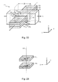
- a second antiferromagnetic memory device 21 is shown.
- the second antiferromagnetic memory device 21 is the same as the first antiferromagnetic memory device 1 ( Figure 1 ) except that the second antiferromagnetic memory device 21 also includes a layer 22 of dielectric material on the antiferromagnetic region 4 and a layer 23 of conductive material on the dielectric layer 22 thereby forming a layer stack 24.
- the dielectric layer 22 comprises crystalline magnesium oxide (MgO) and is sufficiently thin (for example, 2.5 nm) to form a tunnel barrier.
- MgO crystalline magnesium oxide
- Other dielectric materials such as silicon dioxide (SiO 2 ), aluminium oxide (Al 2 O 3 ) or high-k dielectrics such as hafnium oxide (HfO 2 ) can be used.
- the dielectric material may be antiferromagnetic.
- the antiferromagnetic layer 4 is in direct contact with the dielectric layer 22.
- a protective capping layer can be omitted.
- the conductive layer 23 may comprise tantalum (Ta). However, other metals or a semiconductor material can be used. Further details regarding TAMR effect and readout can be found in US 2014/169084 A1 ibid.
- the cross-shaped structure 2 is formed from different materials.
- the cross-shaped structure can be formed from the same material, i.e. a single layer of antiferromagnetic material.
- a third antiferromagnetic memory device 31 is shown.
- the third is the same as the first antiferromagnetic memory device 1 ( Figure 1 ) except that conductive arms 8 1 , 8 2 , 8 3 , 8 4 are also formed from an antiferromagnetic material, for example, the same antiferromagnetic material used to form the antiferromagnetic region 4.
- a single deposition step and a single patterning step can be used.
- the antiferromagnetic region 4 can be modified to reduce its magnetic anisotropy, for example, by implanting helium ions (not shown) or by thinning the region 4, and so facilitate switching at a lower current before the antiferromagnetic conductive arms 8 1 , 8 2 , 8 3 , 8 4 .
- the third antiferromagnetic memory device 31 may be modified by omitting the capping layer (not shown) and providing a tunnel barrier layer (not shown) in direct contact with the antiferromagnetic region 4 and an electrode layer (not shown) on the tunnel barrier layer (not shown) so as to allow TAMR-based readout in the same way as the second memory device 21 ( Figure 5 ).
- a fourth antiferromagnetic memory device 41 is shown.
- the fourth memory device 41 is similar to the first memory device 1 ( Figure 1 ) except that spin current is diffused into the antiferromagnetic region 4 from an underlying cross-shaped structure 42 comprising a paramagnetic or diamagnetic conductive material, such as platinum, tantalum or tungsten.
- the cross-shaped structure 42 includes first, second, third and fourth arms 48 1 , 48 2 , 48 3 , 48 4 .
- Each conductive arm 48 1 , 48 2 , 48 3 , 48 4 has a respective terminal 49 1 ,49 2 , 49 3 , 49 4 at its end.
- the first and third conductive arms 48 1 , 48 3 define a first current path 50 1 through the underlying cross-shaped structure 42.
- the second and fourth arms 48 2 , 48 4 define a second current path 50 2 .
- the first and second current paths 50 1 , 50 2 are orthogonal and are parallel to the first and second easy axes 7 1 , 7 2 .
- the underlying structure 42 is a source of spin-polarized current 51 1 , 51 2 (also referred to herein as a "spin current").
- spin current also referred to herein as a "spin current"
- spin current When a current flows through the paramagnetic or diamagnetic material, along a current path 50 1 , 50 2 , a transverse spin current is generated due to the spin Hall effect.
- spin angular momentum flows, without flow of electrical charge, in a direction perpendicular to the applied electrical current. This is because if spin-up electrons are deflected in, for example, a positive transverse direction, then spin-down electrons are deflected in the opposite direction, i.e. a negative transverse direction.
- spin current 51 1 , 51 2 diffuses into the antiferromagnetic region 4.
- the spin current 51 1 , 51 2 diffuses in a direction which is perpendicular to the interface, i.e. in a direction along the axis 5.
- spin current In conventional magnetic tunnel junctions with two ferromagnetic layers, a spin current can be injected from one ferromagnetic layer magnet serving as a "spin source" to the other ferromagnetic layer acting as a "spin drain".
- spin current should have a component perpendicular to the planes of the two ferromagnetic layers so that the spin current can propagate from the source to the drain.
- the easiest way to achieve this is to drive an electrical current from the source to the drain in the vertical direction (perpendicular to the layer planes).
- the antiferromagnetic region 4 can effectively serve as the spin drain.
- the memory 52 includes an array 53 of cells 54, a row decoder 55, sense amplifiers 56 and a column decoder 57.
- Each cell 54 may be based on an antiferromagnetic memory device 1, 21, 31, 41 hereinbefore described or an antiferromagnetic memory device 81,101, 111 hereinafter described.
- the antiferromagnetic spin axis of an antiferromagnetic region which is formed from a suitable antiferromagnetic material and/or which is suitably configured (e.g. by making it sufficiently thin) can be switched using a current-induced Néel spin-orbit torque.
- heat-assisting writing can also be used in some antiferromagnetic memory device which uses a current-induced Néel spin-orbit torque for writing.
- the antiferromagnetic spin axis can be orientated along one easy axis using Néel spin-orbit torque and can be orientated along another easy axis using hear-assisted writing.
- the antiferromagnetic spin axis can be orientated along the other easy axis by heating the device so that the antiferromagnetic material becomes ferromagnetic or paramagnetic, using an Oersted field to orientate magnetic moments in the ferromagnetic or paramagnetic phase in a direction such that when the antiferromagnetic region cools and become antiferromagnetic, the magnetic moments re-orientate so as to be parallel or antiparallel to the other easy axis (i.e. the antiferromagnetic spin axis becomes orientated along the other easy axis).
- FeRh Iron rhodium
- This property can be exploited in an antiferromagnetic memory device by non-uniformly heating an antiferromagnetic region so that a low-temperature antiferromagnetic phase and a high-temperature ferromagnetic or paramagnetic phase concurrently exist in the storage element separated by a phase boundary.
- Magnetic moments in the high-temperature ferromagnetic or paramagnetic phase can be orientated using an applied magnetic field. This magnetic field may be generated using a conductive line which is also used to heat the antiferromagnetic region.
- Magnetic moments in the ferromagnetic or paramagnetic phase are coupled to magnetic moments in the antiferromagnetic phase by an exchange field.
- the exchange field can be much stronger than the applied magnetic field.
- the ferromagnetic phase can help to stabilise the antiferromagnetic phase.
- the transition temperature is field dependent and so the transient high-temperature ferromagnetic phase can assist transition of the antiferromagnet phase to the ferromagnetic phase.
- Figure 11 is a perspective view of a generally planar antiferromagnet 61 which extends from a first end 62 to a second end 63 between first and second sides 64, 65.
- An elongate heater wire 66 is placed in thermal contact with the antiferromagnet 61 running along one side 64 of the antiferromagnet 61.
- the antiferromagnet 61 and heater wire 66 may be electrically isolated from each other using a region of dielectric material (not shown).
- a current source 67 is arranged to drive current through the heater wire 66.
- the antiferromagnet 61 is formed from FeRh or some other antiferromagnetic material which exhibits a transition between antiferromagnet and ferromagnetic phases and the wire 66 comprises, for example, tungsten (W) or other material having a suitable resistivity, p.
- the wire 66 has dimensions for a given resistivity, p, and current, I H , to generate sufficient heat energy to heat the antiferromagnet 61 to a temperature, T, above the antiferromagnet-ferromagnetic phase transition temperature, T T , for the antiferromagnet.
- the antiferromagnet 61 and wire 66 may be formed by sputtering material on a substrate (not shown) using e-beam lithography and lift-off to pattern the antiferromagnet 61 and wire 66.
- the antiferromagnet 61 may be monocrystalline or polycrystalline.
- the antiferromagnet 61 has an initial temperature which lies below the transition temperature, T T , of the antiferromagnet 61.
- the transition temperature, T T is about 105 °C and so the initial temperature, T 1 , may be room temperature.
- the antiferromagnet 1 contains an antiferromagnetic phase 68 having magnet moments 69 which are orientated along a first magnetic easy axis 70 1 .
- a current, I H is driven through the heater wire 66 which generates heat and increases the temperature of the antiferromagnet 1 adjacent.
- a phase boundary 71 between the antiferromagnetic phase 68 and a ferromagnetic phase 72 propagates through the antiferromagnet 61 away from the wire 66.
- the antiferromagnet 61 has a temperature above the transition temperature, T T , and is ferromagnetic.
- magnetic moments 73 are aligned with the Oersted field 74 generated by the wire 76.
- phase boundary 71 may continue to propagate until the whole antiferromagnet 61 has changed into a ferromagnetic state 72.
- an external magnetic field 75 may applied to the antiferromagnet 61.
- magnetic moments 73 in the ferromagnetic phase 72 may be realigned, for example, along the y-axis.
- the antiferromagnet 61 cools sufficiently, then the antiferromagnetic phase 66 reforms.
- the magnetic moments 69 in the antiferromagnetic phase 68 are coupled via exchange field to the magnetic moments 73 in the ferromagnetic phase 72.
- the magnet moments 69 in the antiferromagnetic phase 68 are orientated along a second magnetic easy axis 70 2 .
- the first and second easy axes 70 1 , 70 2 are orthogonal (i.e. arranged at right angles).
- phase boundary 71 recedes until the whole of the antiferromagnet 61 returns to the antiferromagnetic phase 68, as shown in Figure 12h .
- a separate external magnetic field 75 need not be applied.
- the heater wire 66 may generate not only heat for increasing the temperature of the ferromagnet, but also an in-plane magnetic field.
- Figure 13 is a perspective view of another generally planar antiferromagnet 61 which extends from a first end 62 to a second end 63.
- the width of the antiferromagnet 61 between first and second sides 64, 65 may vary, e.g. by tapering. Additionally or alternatively, the thickness of the antiferromagnet 61' may vary.
- the heater wire is omitted. Instead, the current source 67 is connected between the ends 64, 65 of the antiferromagnet.
- the antiferromagnet 61 has dimensions for a given resistivity, p, and current, I H , to generate sufficient heat energy to heat itself to a temperature, T, above the antiferromagnet-ferromagnetic phase transition temperature, T T , for the antiferromagnet.
- the antiferromagnet 61 has an initial temperature which lies below the transition temperature, T T , of the antiferromagnet 61.
- the antiferromagnet 61 contains an antiferromagnetic phase 68 having magnet moments 69 which are orientated along a first magnetic easy axis 70 1 .
- a current, I H is driven through the antiferromagnet 61.
- the transverse cross-sectional area, A, of the antiferromagnet 61 varies along its length and so the current density, j, varies inversely proportionally to area, A.
- the current density, j 1 proximate to the first end 62 of the antiferromagnet 61 is smaller than the current density, j 2 , close to the second end 63 of the block of antiferromagnetic material. Consequently, the temperature T at the second end 63 of the antiferromagnet 61 may rise at a quicker rate than at the first end 62.
- a phase boundary 71 starts to propagate from the second end 63 towards the first end 62 as a ferromagnetic phase 72 forms.
- phase boundary 71 may continue to propagate until the whole antiferromagnet 61 becomes ferromagnetic.
- an external magnetic field 75 may applied to the antiferromagnet 61.
- magnetic moments 73 in the ferromagnetic phase 72 may be realigned, for example, along the y-axis.
- the antiferromagnet 61 cools sufficiently, then the antiferromagnetic phase 66 re-forms.
- the magnetic moments 69 in the antiferromagnetic phase 68 are coupled via exchange field to the magnetic moments 73 in the ferromagnetic phase 72.
- the magnet moments 69 in the antiferromagnetic phase 68 are orientated along a second magnetic easy axis 70 2 .
- the device 81 generally takes the form of a flat, elongated structure 82 lying on an insulating substrate 83.
- the structure 82 includes a planar antiferromagnetic region 84.
- the antiferromagnetic region 84 exhibits broken inversion symmetry along an out-of-plane axis 85.
- the antiferromagnetic region 84 has an antiferromagnetic spin axis 86 which is orientable along first and second in-plane, orthogonal easy axes 87 1 , 87 2 .
- the antiferromagnetic region 84 comprises di-manganese gold (Mn 2 Au).
- the antiferromagnetic region 4 may be protected by a thin (e.g. ⁇ 2nm) capping layer (not shown) of tantalum (Ta) or other suitable metal or a suitable dielectric material.
- the antiferromagnetic region 84 is supported on a conductive strip 88 having first and second terminals 89 1 , 89 2 between the terminals 89 1 , 89 2 .
- the conductive strip 88 comprises a paramagnetic or diamagnetic conductive material, such as platinum or gold.
- the conductive strip 88 defines a current path 90 through the antiferromagnetic region 84.
- the current path 90 I is parallel to the first easy axis 87 1 .
- the conductive strip 88 is a source of spin-polarized current 91 due to the spin Hall effect in the same way as in fourth antiferromagnetic memory device 41 ( Figure 7 ).
- spin current 91 diffuses into the antiferromagnetic region 84.
- the spin current 91 diffuses in a direction which is perpendicular to the interface, i.e. in a direction along the axis 5.
- a circuit (not shown) used for driving a current through the conductive strip 82 comprises a current source (not shown) coupled to the terminals 89 1 , 89 2 .
- the antiferromagnetic spin axis 86 can be switched from the first to the second easy axis 87 1 , 87 2 using Neel spin-orbit torque in the manner hereinbefore described. This can occur using a current, I, which is at least equal to a threshold current, I NSOT , for current-induced torque-based switching but not so high so such that the temperature, T, of the antiferromagnetic region 84 stays below the phase-change temperature, T T , of the antiferromagnetic region 8 4 , i.e. the temperature at which antiferromagnetic region 84 changes from being antiferromagnetic to being paramagnetic or ferromagnetic.
- the antiferromagnetic spin axis 86 can be switched from the second easy axis 87 2 to the first easy axis 87 1 by passing a sufficiently high current, I, which exceeds a threshold, I HIGH , to cause the temperature of the antiferromagnetic region 4 to exceed the phase-change temperature, T T .
- the current also exceeds a threshold current, I STT , which applies a spin-transfer torque to the magnetic moments 92, for example in a ferromagnetic phase, and causes them to rotate so that they lie along an axis 93 which is perpendicular to the current.
- the current is switched off which results in the antiferromagnetic region 84 cooling below the phase-change temperature, T T .
- the magnetic moments 92 rotate through 90 degrees such that the antiferromagnetic spin axis 86 is perpendicular to the original axis 93.
- Steady or quasi-steady state currents need not be used.
- Current having a time-varying waveform (which may include pulses) can be used.
- short, high-magnitude current pulses can be used to discourage heating, while achieving sufficiently high currents for spin-orbit torque switching.
- longer pulses having a magnitude which do not exceed the threshold current value for spin-orbit torque switching can be used for rapid heating.
- the fifth antiferromagnetic memory device 81 may include a pair of contacts (not shown) for measuring ohmic AMR or a tunnel barrier arrangement for measuring tunnelling AMR as described in US 2014/169084 A1 ibid.
- two crossed lines can provide further degrees of control over heating, allow Oersted fields having different orientations (e.g. perpendicular) to be applied and/or provide a readout arrangement, such as a tunnel barrier arrangement.
- a sixth antiferromagnetic memory device 101 is shown.
- the device 101 is similar to the fifth device 81 except that it includes a second conductive line 102, a thin (e.g. ⁇ 5 nm) dielectric layer 103, such as silicon dioxide (SiO 2 ) or magnesium oxide (MgO), disposed between the antiferromagnetic layer 84 and the second conductive line 102 to form a tunnel barrier configuration 103.
- the substrate 83 ( Figure 16 ) is omitted from Figure 18 for clarity.
- the first and second conductive lines 88,102 many be used to heat the antiferromagnetic layer 84 and provide orthogonal magnetic fields, H.
- the conductive line 88 (or conductive lines 88, 102) can be configured to promote heating and Figures 20 and 21 illustrate two ways of adapting the conductive lines 88. It will be appreciated that if a second conductive 102 line is provided, then it can be adapted in a corresponding way to the other conductive line 88.
- a section (or "length") 105 of a conductive line 88 which is next to the antiferromagnetic region 84 may be thinner than another section 106 of the line 88.
- the transverse cross-sectional area of a conductive line 88 is reduced and so the section 105 has a higher resistance per unit length than the other section 106 of the line 88.
- the section 105 may be narrower than another section 106 of the line 88.
- a seventh antiferromagnetic memory device 111 is shown.
- the seventh antiferromagnetic memory device 111 is similar to the fifth antiferromagnetic memory device 81 ( Figure 15 ) in that a first state can be written using Néel spin-orbit torque and a second state can be written using heat-assisted phase transition and the application of an Oersted field.
- the seventh antiferromagnetic device 111 includes a stacked layer structure 112.
- the stacked layer structure 112 includes a first conductive line 113 and first and second planar antiferromagnetic regions 114 1 , 114 2 (herein after referred to as upper and lower planar antiferromagnetic regions 114 1 , 114 2 ) sandwiching the first conductive line 113.
- Each antiferromagnetic region 114 1 , 114 2 generally extends along the first and second directions, i.e. lies in the x-y plane, and are spaced apart along the third direction (z-axis).
- the first conductive line 113 extends along the first direction (i.e. along x-axis).
- the first conductive line 113 has first and second terminals (not shown) at opposite ends of the line for driving current through the line 113.
- the first conductive line 113 comprises a paramagnetic or diamagnetic conductive material, such as platinum or gold.
- the first conductive line 113 is used to diffuse spin current into the antiferromagnetic regions 114 1 , 114 2 for Néel spin-orbit torque switching.
- the antiferromagnetic regions 114 1 , 114 2 are in the form of elongate lines, i.e. where length, 1, is much greater than width, w (for example w ⁇ 0.1 l). However, the antiferromagnetic regions 114 1 , 114 2 need not take the form of elongate lines and may be, for example, near-square or square, where length, 1, is approximately equal to width, w (for example, 2 l ⁇ w ⁇ 0.51).
- each antiferromagnetic region 1141, 114 2 exhibits broken inversion symmetry along an out-of-plane axis 115.
- the antiferromagnetic region 114 1 , 114 2 each have a respective antiferromagnetic spin axis 116 1 , 116 2 which is orientable along first and second in-plane, orthogonal easy axes 117 1 , 117 2 , 118 1 , 118 2 .
- the antiferromagnetic memory device 111 also includes a second conductive line 119 which is used for heating and for read out.
- the first and second conductive lines 113, 119 cross, preferably at right angles.
- the second conductive line 119 includes a section 120 in which the line 119 splits into first and second portions 119 1 , 119 2 (hereinafter referred to as the upper and lower portions 119 1 , 119 2 ) which define a transverse passage 121.
- the upper portion 119 1 runs over the top of the upper antiferromagnetic region 114 1 and the lower portion 119 2 runs under the lower antiferromagnetic region 114 2 .
- the upper and lower first conductive portions 119 1 , 119 2 sandwich the upper and lower antiferromagnetic regions 114 1 , 114 2 .
- a thin layer 122 1 of dielectric material is interposed between the upper antiferromagnetic region 114 1 and the upper portion 119 1 of the second conductive line 119 thereby forming a tunnel barrier arrangement 123 1 .
- a thin layer 122 2 of dielectric material is interposed between the lower antiferromagnetic region 114 2 and the lower portion 119 2 of the second conductive line 119 thereby forming a second tunnel barrier arrangement 123 2 .
- First and second spacer-like layers 124 1 , 124 2 of dielectric material for example, silicon dioxide (SiO 2 ) or magnesium oxide (MgO), run down the sides of the stack layer structure 112, between the stack layer structure 112 and the side walls of the conductive line 119 so as to avoid electrical shorts.
- dielectric material for example, silicon dioxide (SiO 2 ) or magnesium oxide (MgO)
- the upper dielectric layer 122 1 and the side dielectric layers 124 1 , 124 2 may be provided by the same layer of dielectric material.
- a lower half of the second conductive line 119 and then the stacked layer structure 112 may be formed before a conformal layer of dielectric material is deposited over the stacked layer structure 112 (for instance, by sputtering).
- the second half of the second conductive line 119 can then be formed over the dielectric layer.
- the antiferromagnetic spin axes 116 1 , 116 2 can be switched from the first easy axis 117 1 , 117 2 to the second easy axis 118 1 , 118 2 using Neel spin-orbit torque in the manner hereinbefore described.
- the antiferromagnetic spin axes 116 1 , 116 2 can be switched from the second easy axis 118 1 , 118 2 to the first easy axis 117 1 , 117 2 by passing a sufficiently high current, I, which exceeds a threshold, I HICH , through the second conductive line 119 to cause the temperature of the antiferromagnetic regions 114 1 , 114 2 to exceed the phase-change temperature, T T .
- a current, I B is passed through the first conductive line 113 which orientates magnetic moments 124 1 , 124 2 in the regions 114 1 , 114 2 which are ferromagnetic (or paramagnetic) along axis 125.
- the orientation of the moments 124 1 in the first region 114 1 are antiparallel to the moments 124 2 tin the second region 114 2 .
- the heating current is switched off which results in the antiferromagnetic regions 114 1 , 114 2 cooling below the phase-change temperature, T T .
- the magnetic moments 124 1 ,124 2 flip through 90 degrees such that the antiferromagnetic spin axes 116 1 , 116 2 are perpendicular to the original axis 125.
- the geometry and dimensions of the second conductive line 119 may be adapted so as to promote heating.
- the antiferromagnetic memory device 111 can be read out by measuring tunnelling AMR between the first and second conductive lines 113, 119.
- the antiferromagnetic devices herein described may be fabricated using fabrication techniques, such as deposition, lithography and etching.
- Layer may be deposited, for example by physical deposition processes (such as sputtering) or chemical deposition processes (such as chemical vapour deposition or atomic layer deposition).
- Layers can be patterned by forming a mask, for example, using photolithography, electron-beam lithography or other appropriate lithographic process, etching using, for instance a reactive ion etch, or other suitable dry etch or wet etch, to remove unwanted regions of material and so form patterned layers.
- Antiferromagnetic materials which exhibit a phase change between an antiferromagnetic and ferromagnetic phase other than FeRh can be used.
- an antiferromagnetic material an alloy of Mn and antimony doped with a transition metal, i.e. Mn 2-x A x Sb can be used, where A is a transition metal such as chromium (Cr), tin (Sn), cobalt (Co) or iron (Fe), where x is greater than 0 and less than 1.
- the antiferromagnet consists of a material which exhibits a phase change between antiferromagnet and ferromagnetic phases.
- the antiferromagnet may be formed from iridium manganese (IrMn) or other antiferromagnetic materials which exhibit a transition between antiferromagnet and paramagnetic phases at the Néel temperature.
- IrMn iridium manganese
- heat-assisted writing can still take advantage of the high-temperature paramagnetic phase to stabilise the antiferromagnetic phase.
- inversion symmetry may be broken by making a layer of antiferromagnetic material sufficiently thin.
Landscapes
- Engineering & Computer Science (AREA)
- Computer Hardware Design (AREA)
- Mram Or Spin Memory Techniques (AREA)
- Hall/Mr Elements (AREA)
Priority Applications (1)
| Application Number | Priority Date | Filing Date | Title |
|---|---|---|---|
| EP14186900.8A EP3001470B1 (fr) | 2014-09-29 | 2014-09-29 | Dispositif de mémoire antiferromagnétique |
Applications Claiming Priority (1)
| Application Number | Priority Date | Filing Date | Title |
|---|---|---|---|
| EP14186900.8A EP3001470B1 (fr) | 2014-09-29 | 2014-09-29 | Dispositif de mémoire antiferromagnétique |
Publications (2)
| Publication Number | Publication Date |
|---|---|
| EP3001470A1 true EP3001470A1 (fr) | 2016-03-30 |
| EP3001470B1 EP3001470B1 (fr) | 2017-09-06 |
Family
ID=51619109
Family Applications (1)
| Application Number | Title | Priority Date | Filing Date |
|---|---|---|---|
| EP14186900.8A Active EP3001470B1 (fr) | 2014-09-29 | 2014-09-29 | Dispositif de mémoire antiferromagnétique |
Country Status (1)
| Country | Link |
|---|---|
| EP (1) | EP3001470B1 (fr) |
Cited By (11)
| Publication number | Priority date | Publication date | Assignee | Title |
|---|---|---|---|---|
| EP3185245A1 (fr) * | 2015-12-22 | 2017-06-28 | Hitachi, Ltd. | Dispositif de mémoire antiferromagnétique |
| WO2017213261A1 (fr) * | 2016-06-10 | 2017-12-14 | Tdk株式会社 | Élément de renversement d'aimantation du type utilisant le couplage d'échange, élément à effet magnétorésistif du type utilisant le couplage d'échange, mémoire magnétique du type utilisant le couplage d'échange, circuit logique non volatil et élément neuronal magnétique |
| DE102017122053A1 (de) * | 2017-09-22 | 2019-03-28 | Infineon Technologies Ag | Magnetisches Phasenwechselmaterial zur Wärmeabfuhr |
| EP3474281A1 (fr) * | 2017-10-23 | 2019-04-24 | Hitachi, Ltd. | Mémoire antiferromagnétique |
| CN110212086A (zh) * | 2019-05-14 | 2019-09-06 | 三峡大学 | 一种面内磁化反铁磁磁随机存储器存储单元 |
| WO2019190552A1 (fr) * | 2018-03-30 | 2019-10-03 | Intel Corporation | Logique spin-orbite avec matériau de couplage spin-orbite de néel |
| CN111384235A (zh) * | 2020-03-20 | 2020-07-07 | 河南理工大学 | 一种磁性隧道结及基于磁性隧道结的nsot-mram装置 |
| CN112335063A (zh) * | 2018-04-20 | 2021-02-05 | 伊丽莎白女王在都柏林附近神圣不可分割的三一学院的教务长、研究员、学者及董事会其他成员 | 单个磁性层微波振荡器 |
| EP3828890A1 (fr) * | 2019-11-26 | 2021-06-02 | Consejo Superior de Investigaciones Científicas (CSIC) | Dispositif d'enregistrement antiferromagnétique pliable |
| EP3971896A1 (fr) * | 2020-09-17 | 2022-03-23 | Universität Basel | Dispositif de mémoire antiferromagnétique |
| US11411171B2 (en) | 2018-08-07 | 2022-08-09 | Ip2Ipo Innovations Limited | Non-volatile memory cell |
Families Citing this family (1)
| Publication number | Priority date | Publication date | Assignee | Title |
|---|---|---|---|---|
| US11342500B2 (en) | 2019-07-25 | 2022-05-24 | The Regents Of The University Of California | Antiferromagnetic memory storage devices from magnetic transition metal dichalcogenides |
Citations (2)
| Publication number | Priority date | Publication date | Assignee | Title |
|---|---|---|---|---|
| EP2065886A1 (fr) | 2007-11-27 | 2009-06-03 | Hitachi Ltd. | Dispositif magnétorésistif |
| US20140169084A1 (en) | 2012-12-14 | 2014-06-19 | Hitachi, Ltd. | Memory device |
-
2014
- 2014-09-29 EP EP14186900.8A patent/EP3001470B1/fr active Active
Patent Citations (2)
| Publication number | Priority date | Publication date | Assignee | Title |
|---|---|---|---|---|
| EP2065886A1 (fr) | 2007-11-27 | 2009-06-03 | Hitachi Ltd. | Dispositif magnétorésistif |
| US20140169084A1 (en) | 2012-12-14 | 2014-06-19 | Hitachi, Ltd. | Memory device |
Non-Patent Citations (8)
| Title |
|---|
| A. S. NÚÑEZ ET AL: "Theory of spin torques and giant magnetoresistance in antiferromagnetic metals", PHYSICAL REVIEW B, vol. 73, no. 21, 14 June 2006 (2006-06-14), pages 214426/1 - 214426/9, XP009183308, ISSN: 0163-1829, DOI: 10.1103/PhysRevB.73.214426 * |
| A. SAKUMA ET AL: "First-principles study of the magnetic structures of ordered and disordered Mn-Ir alloys", PHYSICAL REVIEW B, vol. 67, no. 2, 1 January 2003 (2003-01-01), pages 024420/1 - 024420/7, XP055177447, ISSN: 0163-1829, DOI: 10.1103/PhysRevB.67.024420 * |
| B. G. PARK ET AL.: "A spin-valve-like magnetoresistance of an antiferromagnet-based tunnel junction", NATURE MATERIALS, vol. 10, 2011, pages 347 - 351 |
| C. CHAPPERT; A. FERT; F. N. VAN DAU: "The emergence of spin electronics in data storage", NATURE MATERIALS, vol. 6, 2007, pages 813 - 823 |
| C. GOULD ET AL.: "Tunneling Anisotropic Magnetoresistance: A Spin-Valve-Like Tunnel Magnetoresistance Using a Single Magnetic Layer", PHYSICAL REVIEW LETTERS, vol. 93, 2004, pages 117203 |
| J. ZELEZNÝ ET AL: "Relativistic Néel-Order Fields Induced by Electrical Current in Antiferromagnets", PHYSICAL REVIEW LETTERS, vol. 113, no. 15, 1 October 2014 (2014-10-01), pages 157201/1 - 157201/5, XP055177643, ISSN: 0031-9007, DOI: 10.1103/PhysRevLett.113.157201 * |
| L. SZUNYOGH ET AL: "Giant magnetic anisotropy of the bulk antiferromagnets IrMn and IrMn3 from first principles", PHYSICAL REVIEW B, vol. 79, no. 2, 1 January 2009 (2009-01-01), pages 020403/1 - 020403/4, XP055177457, ISSN: 1098-0121, DOI: 10.1103/PhysRevB.79.020403 * |
| S. O. MARIAGER ET AL.: "Imaging the antiferromagnetic to ferromagnetic first order phase transition of FeRh", ARXIV:1301.4164V1 [COND-MAT.MTRL-SCI, 17 January 2013 (2013-01-17) |
Cited By (20)
| Publication number | Priority date | Publication date | Assignee | Title |
|---|---|---|---|---|
| EP3185245A1 (fr) * | 2015-12-22 | 2017-06-28 | Hitachi, Ltd. | Dispositif de mémoire antiferromagnétique |
| WO2017213261A1 (fr) * | 2016-06-10 | 2017-12-14 | Tdk株式会社 | Élément de renversement d'aimantation du type utilisant le couplage d'échange, élément à effet magnétorésistif du type utilisant le couplage d'échange, mémoire magnétique du type utilisant le couplage d'échange, circuit logique non volatil et élément neuronal magnétique |
| CN108780779A (zh) * | 2016-06-10 | 2018-11-09 | Tdk株式会社 | 交换偏置利用型磁化反转元件、交换偏置利用型磁阻效应元件、交换偏置利用型磁存储器、非易失性逻辑电路及磁神经元元件 |
| JPWO2017213261A1 (ja) * | 2016-06-10 | 2019-04-04 | Tdk株式会社 | 交換バイアス利用型磁化反転素子、交換バイアス利用型磁気抵抗効果素子、交換バイアス利用型磁気メモリ、不揮発性ロジック回路および磁気ニューロン素子 |
| US10672446B2 (en) | 2016-06-10 | 2020-06-02 | Tdk Corporation | Exchange bias utilization type magnetization rotational element, exchange bias utilization type magnetoresistance effect element, exchange bias utilization type magnetic memory, non-volatile logic circuit, and magnetic neuron element |
| CN108780779B (zh) * | 2016-06-10 | 2023-04-25 | Tdk株式会社 | 交换偏置利用型磁化反转元件、交换偏置利用型磁阻效应元件、交换偏置利用型磁存储器、非易失性逻辑电路及磁神经元元件 |
| DE102017122053A1 (de) * | 2017-09-22 | 2019-03-28 | Infineon Technologies Ag | Magnetisches Phasenwechselmaterial zur Wärmeabfuhr |
| US10643917B2 (en) | 2017-09-22 | 2020-05-05 | Infineon Technologies Ag | Magnetic phase change material for heat dissipation |
| EP3474281A1 (fr) * | 2017-10-23 | 2019-04-24 | Hitachi, Ltd. | Mémoire antiferromagnétique |
| WO2019190552A1 (fr) * | 2018-03-30 | 2019-10-03 | Intel Corporation | Logique spin-orbite avec matériau de couplage spin-orbite de néel |
| CN112335063B (zh) * | 2018-04-20 | 2024-04-02 | 伊丽莎白女王在都柏林附近神圣不可分割的三一学院的教务长、研究员、学者及董事会其他成员 | 单个磁性层微波振荡器 |
| CN112335063A (zh) * | 2018-04-20 | 2021-02-05 | 伊丽莎白女王在都柏林附近神圣不可分割的三一学院的教务长、研究员、学者及董事会其他成员 | 单个磁性层微波振荡器 |
| US11411171B2 (en) | 2018-08-07 | 2022-08-09 | Ip2Ipo Innovations Limited | Non-volatile memory cell |
| CN110212086B (zh) * | 2019-05-14 | 2023-05-02 | 三峡大学 | 一种面内磁化反铁磁磁随机存储器存储单元 |
| CN110212086A (zh) * | 2019-05-14 | 2019-09-06 | 三峡大学 | 一种面内磁化反铁磁磁随机存储器存储单元 |
| EP3828890A1 (fr) * | 2019-11-26 | 2021-06-02 | Consejo Superior de Investigaciones Científicas (CSIC) | Dispositif d'enregistrement antiferromagnétique pliable |
| CN111384235A (zh) * | 2020-03-20 | 2020-07-07 | 河南理工大学 | 一种磁性隧道结及基于磁性隧道结的nsot-mram装置 |
| CN111384235B (zh) * | 2020-03-20 | 2023-05-23 | 河南理工大学 | 一种磁性隧道结及基于磁性隧道结的nsot-mram装置 |
| EP3971896A1 (fr) * | 2020-09-17 | 2022-03-23 | Universität Basel | Dispositif de mémoire antiferromagnétique |
| WO2022058479A1 (fr) * | 2020-09-17 | 2022-03-24 | Universität Basel | Dispositif de mémoire antiferromagnétique |
Also Published As
| Publication number | Publication date |
|---|---|
| EP3001470B1 (fr) | 2017-09-06 |
Similar Documents
| Publication | Publication Date | Title |
|---|---|---|
| EP3001470B1 (fr) | Dispositif de mémoire antiferromagnétique | |
| US10529775B2 (en) | Two-terminal spintronic devices | |
| US9343658B2 (en) | Magnetic memory bits with perpendicular magnetization switched by current-induced spin-orbit torques | |
| CN103633239B (zh) | 磁存储器及其提供方法和编程方法 | |
| CN104704564B (zh) | 磁性纳米结构中基于自旋霍尔扭矩效应的电栅控式三端子电路及装置 | |
| JP5903278B2 (ja) | 分極層を備える磁気トンネル接合 | |
| KR101405854B1 (ko) | 스핀 토크 스위칭을 보조하는 층을 갖는 스핀 토크 스위칭을 이용하는 자기 스택 | |
| JP5648940B2 (ja) | 磁気トンネル接合において磁界を制御するための装置、方法、メモリ・セル | |
| US8102703B2 (en) | Magnetic element with a fast spin transfer torque writing procedure | |
| CN104051611B (zh) | 磁存储器及其提供方法和编程方法 | |
| KR101338050B1 (ko) | 평면외 자기 터널 접합 셀들을 스위칭하는 방법 | |
| KR20220029381A (ko) | 쌍극자 결합 스핀 궤도 토크 구조 | |
| US10302711B2 (en) | Spin hall effect magnetic structures | |
| WO2019006037A1 (fr) | Réduction du taux d'erreur d'écriture dans une ram magnétoélectrique | |
| KR20120046085A (ko) | 수직 이방성 및 향상층을 갖는 자기 터널 접합 셀들 | |
| US20170033281A1 (en) | Systems and Methods for Implementing Magnetoelectric Junctions Including Integrated Magnetization Components | |
| US20190189912A1 (en) | Structures Enabling Voltage Control of Oxidation Within Magnetic Heterostructures | |
| EP3185245A1 (fr) | Dispositif de mémoire antiferromagnétique | |
| US20140169084A1 (en) | Memory device | |
| EP2882004B1 (fr) | Dispositif de mémoire basé sur magnétorésistance anisotropique | |
| Qi et al. | Antiferromagnetic Spintronics in Magnetic Memory Devices |
Legal Events
| Date | Code | Title | Description |
|---|---|---|---|
| PUAI | Public reference made under article 153(3) epc to a published international application that has entered the european phase |
Free format text: ORIGINAL CODE: 0009012 |
|
| AK | Designated contracting states |
Kind code of ref document: A1 Designated state(s): AL AT BE BG CH CY CZ DE DK EE ES FI FR GB GR HR HU IE IS IT LI LT LU LV MC MK MT NL NO PL PT RO RS SE SI SK SM TR |
|
| AX | Request for extension of the european patent |
Extension state: BA ME |
|
| 17P | Request for examination filed |
Effective date: 20160413 |
|
| RBV | Designated contracting states (corrected) |
Designated state(s): AL AT BE BG CH CY CZ DE DK EE ES FI FR GB GR HR HU IE IS IT LI LT LU LV MC MK MT NL NO PL PT RO RS SE SI SK SM TR |
|
| GRAP | Despatch of communication of intention to grant a patent |
Free format text: ORIGINAL CODE: EPIDOSNIGR1 |
|
| STAA | Information on the status of an ep patent application or granted ep patent |
Free format text: STATUS: GRANT OF PATENT IS INTENDED |
|
| INTG | Intention to grant announced |
Effective date: 20170327 |
|
| GRAS | Grant fee paid |
Free format text: ORIGINAL CODE: EPIDOSNIGR3 |
|
| GRAA | (expected) grant |
Free format text: ORIGINAL CODE: 0009210 |
|
| STAA | Information on the status of an ep patent application or granted ep patent |
Free format text: STATUS: THE PATENT HAS BEEN GRANTED |
|
| AK | Designated contracting states |
Kind code of ref document: B1 Designated state(s): AL AT BE BG CH CY CZ DE DK EE ES FI FR GB GR HR HU IE IS IT LI LT LU LV MC MK MT NL NO PL PT RO RS SE SI SK SM TR |
|
| REG | Reference to a national code |
Ref country code: GB Ref legal event code: FG4D |
|
| REG | Reference to a national code |
Ref country code: CH Ref legal event code: EP Ref country code: AT Ref legal event code: REF Ref document number: 926756 Country of ref document: AT Kind code of ref document: T Effective date: 20170915 |
|
| REG | Reference to a national code |
Ref country code: IE Ref legal event code: FG4D |
|
| REG | Reference to a national code |
Ref country code: DE Ref legal event code: R096 Ref document number: 602014014089 Country of ref document: DE |
|
| REG | Reference to a national code |
Ref country code: NL Ref legal event code: MP Effective date: 20170906 |
|
| REG | Reference to a national code |
Ref country code: LT Ref legal event code: MG4D |
|
| PG25 | Lapsed in a contracting state [announced via postgrant information from national office to epo] |
Ref country code: LT Free format text: LAPSE BECAUSE OF FAILURE TO SUBMIT A TRANSLATION OF THE DESCRIPTION OR TO PAY THE FEE WITHIN THE PRESCRIBED TIME-LIMIT Effective date: 20170906 Ref country code: SE Free format text: LAPSE BECAUSE OF FAILURE TO SUBMIT A TRANSLATION OF THE DESCRIPTION OR TO PAY THE FEE WITHIN THE PRESCRIBED TIME-LIMIT Effective date: 20170906 Ref country code: HR Free format text: LAPSE BECAUSE OF FAILURE TO SUBMIT A TRANSLATION OF THE DESCRIPTION OR TO PAY THE FEE WITHIN THE PRESCRIBED TIME-LIMIT Effective date: 20170906 Ref country code: FI Free format text: LAPSE BECAUSE OF FAILURE TO SUBMIT A TRANSLATION OF THE DESCRIPTION OR TO PAY THE FEE WITHIN THE PRESCRIBED TIME-LIMIT Effective date: 20170906 Ref country code: NO Free format text: LAPSE BECAUSE OF FAILURE TO SUBMIT A TRANSLATION OF THE DESCRIPTION OR TO PAY THE FEE WITHIN THE PRESCRIBED TIME-LIMIT Effective date: 20171206 |
|
| REG | Reference to a national code |
Ref country code: AT Ref legal event code: MK05 Ref document number: 926756 Country of ref document: AT Kind code of ref document: T Effective date: 20170906 |
|
| PG25 | Lapsed in a contracting state [announced via postgrant information from national office to epo] |
Ref country code: LV Free format text: LAPSE BECAUSE OF FAILURE TO SUBMIT A TRANSLATION OF THE DESCRIPTION OR TO PAY THE FEE WITHIN THE PRESCRIBED TIME-LIMIT Effective date: 20170906 Ref country code: ES Free format text: LAPSE BECAUSE OF FAILURE TO SUBMIT A TRANSLATION OF THE DESCRIPTION OR TO PAY THE FEE WITHIN THE PRESCRIBED TIME-LIMIT Effective date: 20170906 Ref country code: GR Free format text: LAPSE BECAUSE OF FAILURE TO SUBMIT A TRANSLATION OF THE DESCRIPTION OR TO PAY THE FEE WITHIN THE PRESCRIBED TIME-LIMIT Effective date: 20171207 Ref country code: RS Free format text: LAPSE BECAUSE OF FAILURE TO SUBMIT A TRANSLATION OF THE DESCRIPTION OR TO PAY THE FEE WITHIN THE PRESCRIBED TIME-LIMIT Effective date: 20170906 Ref country code: BG Free format text: LAPSE BECAUSE OF FAILURE TO SUBMIT A TRANSLATION OF THE DESCRIPTION OR TO PAY THE FEE WITHIN THE PRESCRIBED TIME-LIMIT Effective date: 20171206 |
|
| PG25 | Lapsed in a contracting state [announced via postgrant information from national office to epo] |
Ref country code: NL Free format text: LAPSE BECAUSE OF FAILURE TO SUBMIT A TRANSLATION OF THE DESCRIPTION OR TO PAY THE FEE WITHIN THE PRESCRIBED TIME-LIMIT Effective date: 20170906 |
|
| REG | Reference to a national code |
Ref country code: DE Ref legal event code: R119 Ref document number: 602014014089 Country of ref document: DE |
|
| PG25 | Lapsed in a contracting state [announced via postgrant information from national office to epo] |
Ref country code: CZ Free format text: LAPSE BECAUSE OF FAILURE TO SUBMIT A TRANSLATION OF THE DESCRIPTION OR TO PAY THE FEE WITHIN THE PRESCRIBED TIME-LIMIT Effective date: 20170906 Ref country code: PL Free format text: LAPSE BECAUSE OF FAILURE TO SUBMIT A TRANSLATION OF THE DESCRIPTION OR TO PAY THE FEE WITHIN THE PRESCRIBED TIME-LIMIT Effective date: 20170906 Ref country code: RO Free format text: LAPSE BECAUSE OF FAILURE TO SUBMIT A TRANSLATION OF THE DESCRIPTION OR TO PAY THE FEE WITHIN THE PRESCRIBED TIME-LIMIT Effective date: 20170906 |
|
| REG | Reference to a national code |
Ref country code: CH Ref legal event code: PL |
|
| PG25 | Lapsed in a contracting state [announced via postgrant information from national office to epo] |
Ref country code: IS Free format text: LAPSE BECAUSE OF FAILURE TO SUBMIT A TRANSLATION OF THE DESCRIPTION OR TO PAY THE FEE WITHIN THE PRESCRIBED TIME-LIMIT Effective date: 20180106 Ref country code: AT Free format text: LAPSE BECAUSE OF FAILURE TO SUBMIT A TRANSLATION OF THE DESCRIPTION OR TO PAY THE FEE WITHIN THE PRESCRIBED TIME-LIMIT Effective date: 20170906 Ref country code: IT Free format text: LAPSE BECAUSE OF FAILURE TO SUBMIT A TRANSLATION OF THE DESCRIPTION OR TO PAY THE FEE WITHIN THE PRESCRIBED TIME-LIMIT Effective date: 20170906 Ref country code: SK Free format text: LAPSE BECAUSE OF FAILURE TO SUBMIT A TRANSLATION OF THE DESCRIPTION OR TO PAY THE FEE WITHIN THE PRESCRIBED TIME-LIMIT Effective date: 20170906 Ref country code: EE Free format text: LAPSE BECAUSE OF FAILURE TO SUBMIT A TRANSLATION OF THE DESCRIPTION OR TO PAY THE FEE WITHIN THE PRESCRIBED TIME-LIMIT Effective date: 20170906 Ref country code: SM Free format text: LAPSE BECAUSE OF FAILURE TO SUBMIT A TRANSLATION OF THE DESCRIPTION OR TO PAY THE FEE WITHIN THE PRESCRIBED TIME-LIMIT Effective date: 20170906 |
|
| REG | Reference to a national code |
Ref country code: IE Ref legal event code: MM4A |
|
| REG | Reference to a national code |
Ref country code: BE Ref legal event code: MM Effective date: 20170930 |
|
| PG25 | Lapsed in a contracting state [announced via postgrant information from national office to epo] |
Ref country code: LU Free format text: LAPSE BECAUSE OF NON-PAYMENT OF DUE FEES Effective date: 20170929 Ref country code: MC Free format text: LAPSE BECAUSE OF FAILURE TO SUBMIT A TRANSLATION OF THE DESCRIPTION OR TO PAY THE FEE WITHIN THE PRESCRIBED TIME-LIMIT Effective date: 20170906 |
|
| PLBE | No opposition filed within time limit |
Free format text: ORIGINAL CODE: 0009261 |
|
| STAA | Information on the status of an ep patent application or granted ep patent |
Free format text: STATUS: NO OPPOSITION FILED WITHIN TIME LIMIT |
|
| PG25 | Lapsed in a contracting state [announced via postgrant information from national office to epo] |
Ref country code: DK Free format text: LAPSE BECAUSE OF FAILURE TO SUBMIT A TRANSLATION OF THE DESCRIPTION OR TO PAY THE FEE WITHIN THE PRESCRIBED TIME-LIMIT Effective date: 20170906 Ref country code: CH Free format text: LAPSE BECAUSE OF NON-PAYMENT OF DUE FEES Effective date: 20170930 Ref country code: LI Free format text: LAPSE BECAUSE OF NON-PAYMENT OF DUE FEES Effective date: 20170930 Ref country code: IE Free format text: LAPSE BECAUSE OF NON-PAYMENT OF DUE FEES Effective date: 20170929 Ref country code: DE Free format text: LAPSE BECAUSE OF NON-PAYMENT OF DUE FEES Effective date: 20180404 |
|
| REG | Reference to a national code |
Ref country code: FR Ref legal event code: ST Effective date: 20180706 |
|
| 26N | No opposition filed |
Effective date: 20180607 |
|
| PG25 | Lapsed in a contracting state [announced via postgrant information from national office to epo] |
Ref country code: SI Free format text: LAPSE BECAUSE OF FAILURE TO SUBMIT A TRANSLATION OF THE DESCRIPTION OR TO PAY THE FEE WITHIN THE PRESCRIBED TIME-LIMIT Effective date: 20170906 Ref country code: BE Free format text: LAPSE BECAUSE OF NON-PAYMENT OF DUE FEES Effective date: 20170930 |
|
| PG25 | Lapsed in a contracting state [announced via postgrant information from national office to epo] |
Ref country code: MT Free format text: LAPSE BECAUSE OF NON-PAYMENT OF DUE FEES Effective date: 20170929 |
|
| PG25 | Lapsed in a contracting state [announced via postgrant information from national office to epo] |
Ref country code: FR Free format text: LAPSE BECAUSE OF NON-PAYMENT OF DUE FEES Effective date: 20171106 |
|
| PG25 | Lapsed in a contracting state [announced via postgrant information from national office to epo] |
Ref country code: HU Free format text: LAPSE BECAUSE OF FAILURE TO SUBMIT A TRANSLATION OF THE DESCRIPTION OR TO PAY THE FEE WITHIN THE PRESCRIBED TIME-LIMIT; INVALID AB INITIO Effective date: 20140929 |
|
| PG25 | Lapsed in a contracting state [announced via postgrant information from national office to epo] |
Ref country code: CY Free format text: LAPSE BECAUSE OF FAILURE TO SUBMIT A TRANSLATION OF THE DESCRIPTION OR TO PAY THE FEE WITHIN THE PRESCRIBED TIME-LIMIT Effective date: 20170906 |
|
| PG25 | Lapsed in a contracting state [announced via postgrant information from national office to epo] |
Ref country code: MK Free format text: LAPSE BECAUSE OF FAILURE TO SUBMIT A TRANSLATION OF THE DESCRIPTION OR TO PAY THE FEE WITHIN THE PRESCRIBED TIME-LIMIT Effective date: 20170906 |
|
| PG25 | Lapsed in a contracting state [announced via postgrant information from national office to epo] |
Ref country code: TR Free format text: LAPSE BECAUSE OF FAILURE TO SUBMIT A TRANSLATION OF THE DESCRIPTION OR TO PAY THE FEE WITHIN THE PRESCRIBED TIME-LIMIT Effective date: 20170906 |
|
| PG25 | Lapsed in a contracting state [announced via postgrant information from national office to epo] |
Ref country code: PT Free format text: LAPSE BECAUSE OF FAILURE TO SUBMIT A TRANSLATION OF THE DESCRIPTION OR TO PAY THE FEE WITHIN THE PRESCRIBED TIME-LIMIT Effective date: 20170906 |
|
| PG25 | Lapsed in a contracting state [announced via postgrant information from national office to epo] |
Ref country code: AL Free format text: LAPSE BECAUSE OF FAILURE TO SUBMIT A TRANSLATION OF THE DESCRIPTION OR TO PAY THE FEE WITHIN THE PRESCRIBED TIME-LIMIT Effective date: 20170906 |
|
| PGFP | Annual fee paid to national office [announced via postgrant information from national office to epo] |
Ref country code: GB Payment date: 20240808 Year of fee payment: 11 |