EP2924490A2 - Light guide unit, image display device, and display apparatus - Google Patents
Light guide unit, image display device, and display apparatus Download PDFInfo
- Publication number
- EP2924490A2 EP2924490A2 EP15150145.9A EP15150145A EP2924490A2 EP 2924490 A2 EP2924490 A2 EP 2924490A2 EP 15150145 A EP15150145 A EP 15150145A EP 2924490 A2 EP2924490 A2 EP 2924490A2
- Authority
- EP
- European Patent Office
- Prior art keywords
- light
- light guide
- guide plate
- unit
- image forming
- Prior art date
- Legal status (The legal status is an assumption and is not a legal conclusion. Google has not performed a legal analysis and makes no representation as to the accuracy of the status listed.)
- Granted
Links
Images


Classifications
-
- G—PHYSICS
- G02—OPTICS
- G02B—OPTICAL ELEMENTS, SYSTEMS OR APPARATUS
- G02B27/00—Optical systems or apparatus not provided for by any of the groups G02B1/00 - G02B26/00, G02B30/00
- G02B27/01—Head-up displays
- G02B27/017—Head mounted
- G02B27/0172—Head mounted characterised by optical features
-
- G—PHYSICS
- G02—OPTICS
- G02B—OPTICAL ELEMENTS, SYSTEMS OR APPARATUS
- G02B27/00—Optical systems or apparatus not provided for by any of the groups G02B1/00 - G02B26/00, G02B30/00
- G02B27/01—Head-up displays
- G02B27/0101—Head-up displays characterised by optical features
-
- G—PHYSICS
- G02—OPTICS
- G02B—OPTICAL ELEMENTS, SYSTEMS OR APPARATUS
- G02B27/00—Optical systems or apparatus not provided for by any of the groups G02B1/00 - G02B26/00, G02B30/00
- G02B27/01—Head-up displays
- G02B27/0149—Head-up displays characterised by mechanical features
-
- G—PHYSICS
- G02—OPTICS
- G02B—OPTICAL ELEMENTS, SYSTEMS OR APPARATUS
- G02B27/00—Optical systems or apparatus not provided for by any of the groups G02B1/00 - G02B26/00, G02B30/00
- G02B27/01—Head-up displays
- G02B27/017—Head mounted
- G02B27/0176—Head mounted characterised by mechanical features
-
- G—PHYSICS
- G02—OPTICS
- G02B—OPTICAL ELEMENTS, SYSTEMS OR APPARATUS
- G02B6/00—Light guides; Structural details of arrangements comprising light guides and other optical elements, e.g. couplings
- G02B6/0001—Light guides; Structural details of arrangements comprising light guides and other optical elements, e.g. couplings specially adapted for lighting devices or systems
- G02B6/0011—Light guides; Structural details of arrangements comprising light guides and other optical elements, e.g. couplings specially adapted for lighting devices or systems the light guides being planar or of plate-like form
- G02B6/0081—Mechanical or electrical aspects of the light guide and light source in the lighting device peculiar to the adaptation to planar light guides, e.g. concerning packaging
- G02B6/0086—Positioning aspects
- G02B6/0088—Positioning aspects of the light guide or other optical sheets in the package
-
- G—PHYSICS
- G02—OPTICS
- G02B—OPTICAL ELEMENTS, SYSTEMS OR APPARATUS
- G02B6/00—Light guides; Structural details of arrangements comprising light guides and other optical elements, e.g. couplings
- G02B6/0001—Light guides; Structural details of arrangements comprising light guides and other optical elements, e.g. couplings specially adapted for lighting devices or systems
- G02B6/0011—Light guides; Structural details of arrangements comprising light guides and other optical elements, e.g. couplings specially adapted for lighting devices or systems the light guides being planar or of plate-like form
- G02B6/0081—Mechanical or electrical aspects of the light guide and light source in the lighting device peculiar to the adaptation to planar light guides, e.g. concerning packaging
- G02B6/0093—Means for protecting the light guide
-
- G—PHYSICS
- G02—OPTICS
- G02B—OPTICAL ELEMENTS, SYSTEMS OR APPARATUS
- G02B27/00—Optical systems or apparatus not provided for by any of the groups G02B1/00 - G02B26/00, G02B30/00
- G02B27/01—Head-up displays
- G02B27/0101—Head-up displays characterised by optical features
- G02B2027/011—Head-up displays characterised by optical features comprising device for correcting geometrical aberrations, distortion
-
- G—PHYSICS
- G02—OPTICS
- G02B—OPTICAL ELEMENTS, SYSTEMS OR APPARATUS
- G02B27/00—Optical systems or apparatus not provided for by any of the groups G02B1/00 - G02B26/00, G02B30/00
- G02B27/01—Head-up displays
- G02B27/0101—Head-up displays characterised by optical features
- G02B2027/0132—Head-up displays characterised by optical features comprising binocular systems
-
- G—PHYSICS
- G02—OPTICS
- G02B—OPTICAL ELEMENTS, SYSTEMS OR APPARATUS
- G02B27/00—Optical systems or apparatus not provided for by any of the groups G02B1/00 - G02B26/00, G02B30/00
- G02B27/01—Head-up displays
- G02B27/0149—Head-up displays characterised by mechanical features
- G02B2027/0161—Head-up displays characterised by mechanical features characterised by the relative positioning of the constitutive elements
-
- G—PHYSICS
- G02—OPTICS
- G02B—OPTICAL ELEMENTS, SYSTEMS OR APPARATUS
- G02B27/00—Optical systems or apparatus not provided for by any of the groups G02B1/00 - G02B26/00, G02B30/00
- G02B27/01—Head-up displays
- G02B27/017—Head mounted
- G02B27/0172—Head mounted characterised by optical features
- G02B2027/0174—Head mounted characterised by optical features holographic
-
- G—PHYSICS
- G02—OPTICS
- G02B—OPTICAL ELEMENTS, SYSTEMS OR APPARATUS
- G02B27/00—Optical systems or apparatus not provided for by any of the groups G02B1/00 - G02B26/00, G02B30/00
- G02B27/01—Head-up displays
- G02B27/017—Head mounted
- G02B2027/0178—Eyeglass type
Definitions
- the present disclosure relates to a light guide unit, image display device, and display apparatus.
- Japanese Patent Application Laid-Open No. 2006-162767 describes a virtual image display device (image display device), for example.
- This virtual image display device is well known to provide two-dimensional (2D) images as enlarged virtual images by a virtual-image optical system.
- the 2D images are those formed by an image forming unit and provided to be viewed by viewers.
- This image display device 1100 includes, as shown in the conceptual view of Fig. 38 , an image forming unit 111, a collimator optical system 112, and a light guide section 120.
- the image forming unit 111 includes a plurality of pixels that are arranged in a 2D matrix.
- the collimator optical system 112 collimates light coming from each of the pixels in the image forming unit 111.
- the light guide section 120 guides and emits the resulting collimated light coming from the collimator optical system 112. The light emitted from the light guide section 120 is then guided to eyes 21 of a viewer 20.
- the light guide section 120 is configured by a light guide plate 121, and first and second deflection sections 130 and 140.
- the light guide plate 121 propagates therein the incoming light by total reflection, and then emits the light.
- the first deflection section 130 is a single-layer light reflection film, for example, and reflects the light entered the light guide plate 121 so as to achieve total reflection therein.
- the second deflection section 140 is a multi-layer light reflection film in the multi-layer film structure, and emits the light from the light guide plate 121 after the light is propagated therein by total reflection. If such an image display device 1100 configures an HMD, for example, the resulting display apparatus may be reduced in weight and size.
- Japanese Patent Application Laid-Open No. 2007-094175 describes a virtual image display device (image display device) using a holographic diffraction grating, for example.
- This image display device 1300 basically includes, as shown in the conceptual view of Fig. 39 , the image forming unit 111 that displays images, the collimator optical system 112, and a light guide section 320.
- a light guide section 320 In the light guide section 320, light coming from the image forming unit 111 is guided to the eyes 21 of the viewer 20.
- a light guide section 320 includes a light guide plate 321, and first and second diffraction grating members 330 and 340.
- the first and second diffraction grating members 330 and 340 are each a reflective volumetric holographic diffraction grating provided to the light guide plate 321.
- Collimated light from the collimator optical system 112 enters a first plane 322 of the light guide plate 321, and then is emitted from the first plane 322.
- the light guide plate 321 has a second plane 323, which is parallel to the first plane 322 thereof.
- the second plane 323 is attached with the first and second diffraction grating members 330 and 340.
- Such image display devices as above have degradation problems of display images to be viewed by a viewer, e.g., pixel displacement in images or deformed images, due to deviation of light caused by the light being guided by the expanded/contracted light guide plate.
- the expansion/contraction of the light guide plate is resulted from a temperature difference between the outside air and the viewer's body when the light guide plate is exposed to the outside air, or a transient change of temperature when the viewer moves in/out from a room, for example.
- a difference of thermal expansion coefficients between the members in the light guide section is also a cause.
- 2010-087560 describes a head-mounted image display device in which a rod-shaped light guide section is elastically retained by a retaining section to be able to change in position.
- a rod-shaped light guide section is elastically retained by a retaining section to be able to change in position.
- the retaining section at least a part for retaining an end portion of the rod-shaped light guide section is elastic.
- the light guide section being retained at an end portion by the elastic part does not solve the degradation problems of display images, which are caused by the expanded/contracted light guide plate resulted from an environmental temperature change or a difference of thermal expansion coefficients between the members in the light guide unit.
- a light guide unit configured to prevent, without fail, the degradation problems of display images, which are caused by the expanded/contracted light guide plate resulted from an environmental temperature change or a difference of thermal expansion coefficients between the members therein. It is also desirable to provide an image display device including such a light guide unit, and a display apparatus including such an image display device.
- some embodiments relate to a display apparatus and, more specifically, to a display apparatus for use as a head mounted display (HMD), for example, and also to an image display device suitable for use in the display apparatus, and a light guide unit suitable for use in the image display device.
- HMD head mounted display
- an image display device comprising: an image forming unit; and a light guide unit, the light guide unit including a light guide plate configured to guide light of an image formed in the image forming unit, and a support member, the light guide plate being supported by one or more buffer members at, at least, a plurality of portions of the support member.
- an image display device comprising: an image forming unit; and a light guide unit, the light guide unit including a light guide plate configured to guide light of an image formed in the image forming unit, and a support member, the light guide plate and the support member including therebetween a fixing member, the fixing member being provided around the light guide plate to fix the light guide plate to the support member.
- a light guide unit comprising: a light guide plate; and a support member, the light guide plate being supported by one or more buffer members, the one or more buffer members supporting the light guide plate at, at least, a plurality of portions of the support member.
- a light guide unit comprising: a light guide plate; and a support member, the light guide plate and the support member including therebetween a fixing member, the fixing member being provided around the light guide plate to fix the light guide plate to the support member.
- a display apparatus comprising: a frame; and an image display device attached to the frame, the image display device including an image forming unit, and a light guide unit, the light guide unit including a light guide plate configured to guide light of an image formed in the image forming unit, and a support member, the light guide plate being supported by one or more buffer members, the one or more buffer members supporting the light guide plate at, at least, a plurality of portions of the support member.
- a display apparatus comprising: a frame; and an image display device attached to the frame, the image display device including an image forming unit, and a light guide unit, the light guide unit including a light guide plate configured to guide light of an image formed in the image forming unit, and a support member, the light guide plate and the support member including therebetween a fixing member, the fixing member being provided around the light guide plate to fix the light guide plate to the support member.
- a light guide unit including a light guide plate, and a support member, the light guide plate being supported by a buffer member at a plurality of portions of the support member.
- a light guide unit including a light guide plate, and a support member, the light guide plate and the support member including therebetween a fixing member, the fixing member being provided around the light guide plate to fix the light guide plate to the support member.
- an image display device including an image forming unit, and a light guide unit, the light guide unit including a light guide plate, and a support member, the light guide plate being configured to guide light of an image formed in the image forming unit.
- the light guide plate is supported by a buffer member at a plurality of portions of the support member.
- the light guide plate and the support member include therebetween the fixing member, the fixing member being provided around the light guide plate to fix the light guide plate to the support member.
- a display apparatus including a frame configured to be mounted on a viewer's head portion, and an image display device attached to the frame, the image display device including an image forming unit, and a light guide unit, the light guide unit including a light guide plate configured to guide light of an image formed in the image forming unit, and a support member.
- the light guide plate is supported by a buffer member at a plurality of portions of the support member.
- the light guide plate and the support member include therebetween a fixing member, the fixing member being provided around the light guide plate to fix the light guide plate to the support member.
- the light guide plate is supported by the support member using the buffer member at a plurality of portions.
- Such a configuration can prevent, without fail, the degradation problems of display images that are caused by the expanded/contracted light guide plate resulted from an environmental temperature change or a difference of thermal expansion coefficients between the members in the light guide unit.
- Such a configuration also can retain the light guide plate with sufficient stability.
- the fixing member for use to fix the light guide plate to the support member is disposed therebetween and around the light guide plate.
- Such a configuration can prevent, without fail, the degradation problems of display images that are caused by the expanded/contracted light guide plate resulted from an environmental temperature change or a difference of thermal expansion coefficient between the members in the light guide unit. Such a configuration also can retain the light guide plate with sufficient stability. Note that the effects described in this Specification are by way of example only and in no way restrictive, and any additional effects are to be applied.
- the expression of "light guide unit or others in the first embodiment of the present disclosure” means a light guide unit in a first embodiment of the present disclosure, a light guide unit in an image display device in the first embodiment of the present disclosure, and a light guide unit in a display apparatus in the first embodiment of the present disclosure.
- the expression of "light guide unit or others in the second embodiment of the present disclosure” means a light guide unit in a second embodiment of the present disclosure, a light guide unit in an image display device in the second embodiment of the present disclosure, and a light guide unit in a display apparatus in the second embodiment of the present disclosure.
- a light guide plate is supported at a plurality of portions of a support member opposed to each other with the light guide plate being sandwiched therebetween.
- the buffer member may have an elastic modulus lower than that of the light guide plate.
- the buffer member may be made of resin.
- the support member may be shaped like a picture frame to be around the light guide plate.
- the resin for the buffer member is specifically exemplified by epoxy resin, modified silicone resin, epoxy-modified silicone resin, or urethane resin.
- the buffer member may also be made of a porous material, specifically including porous alumina, porous silicon carbide, porous carbon, sintered porous plastic media, and others, or silica aerogel.
- a fixing member may be provided with a buffer area. If this is the configuration, the buffer area may be formed with a void or a notch section.
- the fixing member may be a spring that is specifically exemplified by a leaf spring or a meandering spring. Still alternatively, the fixing member may be an adhesive layer. If this is the configuration, the adhesive layer may be formed with a void or a notch section.
- the fixing member or the adhesive layer serving as the fixing member may be specifically made of epoxy resin, modified silicone resin, epoxy-modified silicone resin, urethane resin, acrylic resin, or others, but this is not restrictive.
- the buffer area may be provided to the light guide plate on the outer circumferential portion thereof, and if this is the configuration, the buffer area may be formed with a void or a notch section. Still alternatively, the buffer area may be provided to the support member on the inner circumferential portion thereof, and if this is the configuration, the buffer area may be formed with a void or a notch section.
- the void or the notch section may be left as it is, or may be filled with a material having an elastic modulus lower than that of the member formed with the void or the notch section.
- the void or the notch section may be desirably extended along the longitudinal direction of the light guide plate.
- the buffer member may
- the top surface of the support member on the opposite side to a viewer, or in some cases, the surface (second plane) of the light guide plate on the opposite side to the viewer may desirably be provided with a protection member (protection plate) for protecting the light guide plate.
- the support member may be made of various types of materials that are described for the light guide plate, or may be made of a metal or alloy material including magnesium alloy, aluminum, and aluminum alloy, for example.
- the material for the light guide plate is specifically exemplified by a transparent glass substrate including soda lime glass and super white glass, an optical glass including quartz glass and BK7, a plastic substrate, a plastic sheet, and a plastic film.
- the plastic material is exemplified by polyethylene terephthalate, polyethylene naphthalate, polycarbonate, cellulose ester such as acetylcellulose, fluorinated polymer such as copolymer of polyvinylidene difluoride or polytetrafluoroethylene and hexafluoropropene, polyether such as polyoxymethylene, polyacetal, polystyrene, polyethylene, polypropylene, polyolefin such as methylpentene polymer, polyimide including polyamideimide, or polyetherimide, polyamide, polyethersulfone, polyphenylene sulfide, polyvinylidene difluoride, tetraacetyl cellulose, bromphenoxy, polyarylate,
- such a light guide unit in various desirable configurations as above may be provided with a dimmer unit.
- the dimmer unit may be attached to the light guide plate or to the frame, for example. The provision of such a dimmer unit may prevent degradation of images for viewing by a viewer that is caused by light from outside, and may obtain high-contrast images for viewing by the viewer.
- the light guide unit may be transmissive or semi-transmissive (see-through type).
- at least a part of the light guide unit facing the eyes of a viewer may be transmissive or semi-transmissive (see-through), and through such a part of the light guide unit, the viewer may see the outside view.
- the display apparatus in the first or second embodiment of the present disclosure may include one image display device (monocular type), or two image display devices (binocular type).
- the first deflection section reflects light directed into the light guide unit, and the second deflection section passes through and reflects the light after the light is propagated in the light guide plate by total reflection.
- the first deflection section may serve as a reflection mirror, and the second deflection section may serve as a semi-transmissive mirror.
- the first deflection section may be made of metal including alloy to serve as a light reflection film (a kind of mirror) that reflects the light directed into the light guide plate.
- the first deflection section may be a multi-layer film structure of a plurality of dielectric layers, a half mirror, or a polarized beam splitter.
- the first deflection section reflects at least a part of the collimated light directed into the light guide plate so as to achieve total reflection of the light in the light guide plate.
- the second deflection section reflects the collimated light for a plurality of times after the light is propagated by total reflection in the light guide plate. The light remains collimated when it is emitted from the light guide plate.
- the second deflection section may be a multi-layer film structure of a plurality of dielectric layers, a half mirror, a polarized beam splitter, or a holographic diffraction grating film.
- These first and second deflection sections are both provided in the light guide plate (incorporated in the light guide plate), and the first deflection section reflects the collimated light directed into the light guide plate so as to achieve total reflection of the light in the light guide plate.
- the second deflection section reflects or diffracts the collimated light for a plurality of times after the light is propagated by total reflection in the light guide plate. The light remains collimated when it is emitted from the light guide plate.
- the first deflection section may diffract and reflect the light directed into the light guide plate
- the second deflection section may diffract and reflect the light for a plurality of times after the light is propagated by total reflection in the light guide plate.
- the first and second deflection sections may be each configured by a diffraction grating element.
- These diffraction grating elements may be each a reflective diffraction grating element or a transmissive diffraction grating element, or one of the diffraction grating elements may be a reflective diffraction grating element, and the remaining diffraction grating element may be a transmissive diffraction grating element.
- the reflective diffraction grating element is exemplified by a reflective volumetric holographic diffraction grating.
- first deflection section being a reflective volumetric holographic diffraction grating
- second deflection section being a reflective volumetric holographic diffraction grating
- the display apparatus in the first or second embodiment of the present disclosure offers image display in a color, e.g., green.
- the first deflection section for use may be a laminate structure of two diffraction grating members, each of which corresponds to one-half of the viewing angle.
- the first and second deflection sections may be each a laminate structure of P diffraction grating members in order to be ready for diffraction and reflection of P types of light in P different wavelength bands (or wavelengths), e.g., P is 3 for red, green, and blue.
- the diffraction grating members are each formed with an interference pattern corresponding to one wavelength band (or wavelength).
- one-layer diffraction grating member may be formed with P types of interference patterns.
- first to third light guide plates may be stacked together with an interval thereamong.
- the first light guide plate is provided with a diffraction grating member being a layer of reflective volumetric holographic diffraction grating that diffracts and reflects light in a red wavelength band (or wavelength).
- the second light guide plate is provided with a diffraction grating member being a layer of reflective volumetric holographic diffraction grating that diffracts and reflects light in a green wavelength band (or wavelength).
- the third light guide plate is provided with a diffraction grating member being a layer of reflective volumetric holographic diffraction grating that diffracts and reflects light in a blue wavelength band (or wavelength).
- Such configurations accordingly increase the diffraction efficiency, increase the angle available for diffraction, and optimize the angle at which diffraction and reflection occur when the light in each wavelength band (or wavelength) is diffracted and reflected in the diffraction grating members.
- the first and second diffraction grating members are each made of a photopolymer material.
- the first and second diffraction grating members each being a reflective volumetric holographic diffraction grating may be the same as a previous reflective volumetric holographic diffraction grating in terms of basic material and configuration.
- the reflective volumetric holographic diffraction grating means a holographic diffraction grating that diffracts and reflects only +1 order diffracted light.
- the diffraction grating member is formed with an interference pattern from the inside to the surface, and the interference pattern itself may be formed similarly to a previous interference pattern.
- a substance to be a diffraction grating member e.g., photopolymer material
- a substance to be a diffraction grating member may be exposed to object light from a first predetermined direction on one side, and at the same time, the substance is also exposed to reference light from a second predetermined direction on the other side.
- Such exposure to the object light and the reference light accordingly forms an interference pattern, and the resulting interference pattern may be recorded inside of the substance.
- the resulting interference pattern may have a desired pitch and a desired slant angle on the surface of the diffraction grating member.
- the slant angle of the interference pattern means an angle at which the surface of the diffraction grating member (or the diffraction grating layer) forms with the interference pattern.
- the first and second diffraction grating members are each a laminate structure of P diffraction grating layers each being a reflective volumetric holographic diffraction grating
- the P diffraction grating layers may be formed separately, and then stacked (bonded) one on the other using a UV (ultraviolet) curing agent.
- a diffraction grating layer may be first formed using an adhesive photopolymer material, and for attachment thereon, other diffraction grating layers may be then formed one by one also using an adhesive photopolymer material.
- the image forming unit may include a plurality of pixels arranged in a 2D matrix.
- Such an image forming unit may be referred to as "first image forming unit" for convenience.
- the first image forming unit may be configured by a reflective spatial light modulator and a light source, by a transmissive spatial light modulator and a light source, or by a light-emitting element such as light-emitting diode (LED), semiconductor laser element, organic EL (Electro Luminescence) element, or inorganic EL element.
- the desirable image forming unit is configured by a reflective spatial light modulator and a light source.
- the spatial light modulator is exemplified by a light bulb, including a transmissive or reflective liquid crystal display such as LCOS (Liquid Crystal On Silicon), and a digital micro mirror device (DMD).
- the light source is exemplified by the above-mentioned light-emitting element.
- the reflective spatial light modulator may be a polarized beam splitter with which light coming from the liquid crystal display and the light source is partially reflected and directed to the liquid crystal display, and the light reflected by the liquid crystal display is partially passed and directed to the optical system.
- the light-emitting element for the light source includes red, green, blue, and white light emitting elements.
- the light emitted from these red, green, and blue light-emitting elements, i.e., red, green, and blue light may be mixed and made uniform in luminance using a light bulb to obtain white light.
- Such light-emitting elements may be each a semiconductor laser element, a solid laser, or an LED, for example.
- the number of the pixels may be determined based on the performance specifications expected for the image display device, and the specific number of the pixels may be 320 ⁇ 240, 432 ⁇ 240, 640 ⁇ 480, 854 ⁇ 480, 1024 ⁇ 768, or 1920 ⁇ 1080, for example.
- the collimator optical system that will be described later is capable of converting information about pixel position into information about angle of the light guide section in the optical system.
- the collimator optical system has the positive optical power as a whole, and is a convex lens, a concave lens, a free-shaped prism, or a holographic lens, or a combination thereof, for example.
- the image forming unit may include a light source, and a scanning section that scans collimated light coming from the light source.
- a scanning section that scans collimated light coming from the light source.
- Such an image forming unit may be referred to as "second image forming unit" for convenience.
- the light source in the second image forming unit may be a light-emitting element, specifically including red, green, blue, and white light-emitting elements.
- the light emitted from these red, green, and blue light-emitting elements i.e., red, green, and blue light
- Such light-emitting elements may be each a semiconductor laser element, a solid laser, or an LED, for example.
- the number of the pixels (virtual pixels) in the second image forming unit may also be determined based on the performance specifications expected for the image display device, and the specific number of the pixels (virtual pixels) may be 320 ⁇ 240, 432 ⁇ 240, 640 ⁇ 480, 854 ⁇ 480, 1024 ⁇ 768, or 1920 ⁇ 1080, for example.
- a cross prism is desirably used for color composition, for example.
- the scanning section scans horizontally and vertically light coming from the light source, and may be a MEMS (Micro Electro Mechanism Systems) including a micro mirror that is rotatable in the 2D direction, or a galvano mirror, for example.
- MEMS Micro Electro Mechanism Systems
- a relay optical system that will be described next may be a well-known relay optical system.
- the optical system collimates light, and directs the resulting collimated light beams into the light guide plate.
- Such an optical system is sometimes referred to as "collimator light emitting optical system", and is specifically a collimator optical system or a relay optical system.
- the reason for the light to remain collimated is that information about optical wavefront when such light beams are directed into the light guide plate is expected to be stored even after the light beams are emitted therefrom via the first and second deflection sections.
- a light emitting section of the image forming unit may be positioned at the focal length in the collimator light emitting optical system, for example.
- the collimator light emitting optical system is capable of converting information about pixel position into information about angle of the light guide section in the optical system.
- the collimator light emitting optical system has the positive optical power as a whole, and is a convex lens, a concave lens, a free-shaped prism, or a holographic lens, or a combination thereof, for example.
- the image forming unit or the light source configured by light-emitting elements and a light bulb
- the following configurations may be also possible other than the combination of a backlight that emits white light as a whole, and a liquid crystal display including red, green, and blue light-emitting pixels.
- An image forming unit A may include
- the image forming unit A controls light-emission/no light-emission of the first, second, and third light-emitting elements.
- An image forming unit B includes
- Image display is performed by the light-pass control units controlling light-pass/no light-pass of light coming from the light-emitting elements.
- a section (light directing member) in use may be a light guide member, a micro lens array, a mirror, a reflection plate, or a condenser lens, for example.
- An image forming unit C includes
- Image display is performed by the light-pass control units (light bulbs) controlling light-pass/no light-pass of light coming from these first, second, and third light-emitting panels.
- light-pass control units light bulbs
- An image forming unit D is a field-sequential color image forming unit, including
- Image display is performed by the light-pass control unit controlling light-pass/no light-pass of light coming from these light-emitting elements.
- An image forming unit E is also a field-sequential color image forming unit, including
- Image display is performed by the light-pass control unit controlling light-pass/no light-pass of light coming from these light-emitting panels.
- An image forming unit F is a passive- or active-matrix color image forming unit configured to perform image display by controlling light-emission/no light-emission of first, second, and third light-emitting elements.
- An image forming unit G is a field-sequential color image forming unit, including a light-pass control unit (light bulb) configured to control light-pass/no light-pass of light coming from light-emitting element units arranged in a 2D matrix.
- Image display is performed by time-sharing control executed over light-emission/no light-emission of first, second, and third light-emitting elements in the light-emitting element units, and by the light-pass control unit controlling light-pass/no light-pass of light coming from first, second, and third light-emitting elements.
- the light guide plate is provided to be closer as a whole to the center side of the viewer's face than the image forming units
- a coupling member is further provided to couple the two image display devices, the coupling member is attached to the center portion of a frame on the side facing the viewer, the frame being positioned between the viewer's two eyes, and a projection image of the coupling member is in a projection image of the frame.
- the coupling member is attached to the center portion of the frame positioned between the viewer's two eyes, that is, if the image display devices are not directly attached to the frame, temple sections are extended outward when the viewer wears the frame on his head portion. Therefore, even if the frame is deformed, the frame deformation does not cause displacement (position change) of the image forming units or the light guide plate, and even if such displacement occurs, the displacement is negligible.
- Such a configuration thus prevents a change of convergence angle between right and left images without fail.
- the configuration eliminates having to increase the rigidity of the front part of the frame so that the frame is not increased in weight, the design ability is not impaired, and the cost is not increased.
- the frame may be in various designs and colors to meet the viewer's preferences, and the frame designing is less restricted and highly flexible.
- the coupling member is positioned between the viewer and the frame, and the projection image of the coupling member is in the projection image of the frame, i.e., when the head mounted display is viewed from the front of the viewer, the coupling member is hidden behind the frame. This offers the head mounted display with sophistication and refinement of design.
- the coupling member is attached to the center portion of a front section on the side facing the viewer.
- the front section is positioned between the viewer's two eyes, and corresponds to a bridge section of ordinary glasses.
- the image forming units may be respectively attached to end portions of the coupling member to be adjustable.
- the image forming units are desirably positioned outside of the viewer's eyes.
- Such a configuration also desirably satisfies 0.01 ⁇ L ⁇ ⁇ ⁇ 0.30 ⁇ L, or 0.05 ⁇ L ⁇ ⁇ ⁇ 0.25 ⁇ L, 0.35 ⁇ L ⁇ ⁇ ⁇ 0.65 ⁇ L, or 0.45 ⁇ L ⁇ ⁇ ⁇ 0.55 ⁇ L, 0.70 ⁇ L ⁇ ⁇ ⁇ 0.99 ⁇ L, or 0.75 ⁇ L ⁇ ⁇ ⁇ 0.95 ⁇ L, where ⁇ denotes a distance from the attachment center for one of the image forming units to one end portion (one endpiece) of the frame, ⁇ denotes a distance from the center of the coupling member to the one end portion (the one endpiece) of the frame, ⁇ denotes a distance
- the image forming units For respectively attaching the image forming units to the end portions of the coupling member, specifically, three through holes are formed to each of the end portions of the coupling member, and screw sections corresponding to these through holes are formed to each of the image forming units. Thereafter, screws are fastened into the screw sections formed to the image forming units through the through holes. Between each of the screws and each of the screw sections, a spring is inserted in advance. Therefore, by controlling the degree of screw fastening, the image forming units may be adjusted in state of attachment, i.e., adjusted in angle with respect to the coupling member.
- the expression of "the attachment center for the image forming unit” denotes a point at which an overlapped portion between the projection image of the image forming unit and the projection image of the frame is divided equally into two along the axis of the frame.
- the projection images are those obtained by projecting the image forming unit and the frame onto a virtual plane when the image forming unit is attached to the coupling member.
- the expression of "the center of the coupling member” denotes, when the coupling member is attached to the frame, a point at which a portion where the coupling member is in contact with the frame is divided equally into two along the axis of the frame.
- the expression of "the length of the frame” means the length of the projection image of the frame when the frame is bent. Note that the projection direction is vertical to the viewer's face.
- the coupling member may couple together two light guide plates.
- the two light guide plates may be integrally manufactured. If this is the case, the coupling member is coupled to the integrally-manufactured light guide plate, and this configuration is also regarded as the coupling member coupling together two light guide plates.
- the center of the image forming unit denotes a point at which an overlapped portion between the projection image of the image forming unit and the projection image of the frame is divided equally into two along the axis of the frame.
- the projection images are those obtained by projecting the image forming unit and the frame onto a virtual plane when the image forming unit is attached to the light guide plate.
- the shape of the coupling member is essentially arbitrary as long as the projection image thereof is in the projection image of the frame, e.g., like a rod or a slim plate.
- the material for the coupling member may be metal, alloy, plastic, or a combination thereof.
- a light beam emitted from the center of the image forming unit and passed through a node in the optical system on the side of the image forming unit is referred to as "center light beam", and a part of the center light beam vertically entering the light guide unit is referred to as "at-center incident light beam".
- the point at which the at-center incident light beam enters the light guide unit is referred to as "light-guide-unit center point”.
- the axis passing through the light-guide-unit center point and being parallel to the axis of the light guide unit is referred to as "X axis”
- Z axis the axis passing through the light-guide-unit center point and coinciding with the normal to the light guide unit
- the horizontal direction is parallel to the X axis, and hereinafter, may sometimes referred to as "X-axis direction".
- the optical system is disposed between the image forming unit and the light guide unit, and collimates light coming from the image forming unit. The resulting collimated luminous flux is directed into the light guide unit, is guided therein, and is emitted therefrom.
- the center point of the first deflection section is the "light-guide-unit center point".
- the light guide plate includes two parallel planes (first and second planes) extending parallel to the axis of the light guide plate, i.e., longitudinal direction, horizontal direction, and corresponds to the X axis.
- the width direction of the light guide plate corresponds to the Y axis.
- the first plane may serve both as the light-guide-plate incident plane and the light-guide-plate exit plane, or the first plane may serve as the light-guide-plate incident plane, and the second plane may serve as the light-guide-plate exit plane.
- the interference pattern on the diffraction grating member is extended substantially parallel to the Y axis.
- the frame may be configured by a front section, and two temple sections.
- the front section is disposed to be in front of a viewer, and the temple sections are respectively attached to the ends of the front section via hinges to be able to rotate.
- the tip end portion of each of the temple sections is attached with a temple tip section.
- the image forming unit may be attached to the temple sections.
- the front section and the two temple sections may be integrally manufactured. That is, when the display apparatus in the first or second embodiment is viewed in its entirety, the frame looks substantially the same as that of ordinary glasses.
- the material for the frame may be same as that for the ordinary glasses, e.g., metal, alloy, plastic, or a combination thereof.
- the front section may be provided with a nose pad. That is, when the display apparatus in the first or second embodiment is viewed in its entirety, the structure of the frame with the nose pad looks substantially the same as that of the ordinary glasses except that there is no rim.
- the nose pad may also be in the well-known structure and configuration.
- a wiring line (signal line or power supply line) from one or two image forming units goes through the temple section and the temple tip section to be outside from the tip end portion of the temple tip sections, and then is connected to a control unit (control circuit or control section).
- the image forming unit may be provided with a headphone section, and if this is the configuration, a headphone-use wiring line from the image forming unit goes through the temple section and the temple tip section to reach the headphone section via the tip end portion of the temple tip section.
- the headphone section may be of an in-ear type or a canal type, for example.
- the headphone-use wiring line goes around behind the pinna from the tip end portion of the temple tip section, and reaches the headphone section.
- an imaging unit may be attached to the center or end portion of the front section, or to the temple sections, for example.
- a wiring line from the imaging unit may be connected to the image display device (or the image forming unit) via the front section, or may be merged with another wiring line extending from the image display device (or the image forming unit), for example.
- the dimmer unit When the display apparatus includes a dimmer unit, the dimmer unit includes first and second substrates, the first substrate opposing the light guide unit, the second substrate opposing the first substrate, first and second electrodes respectively provided to the first and second substrates, and a light-transmission control material layer sealed between the first and second substrates.
- the first substrate may also be a component in the light guide unit.
- the display apparatus in such a configuration is referred to as "first display apparatus" for convenience.
- first display apparatus In the first display apparatus, with the first substrate in the dimmer unit being also a component in the light guide unit, the entire weight reduced so that this does not cause discomfort to a user of the display apparatus.
- the second substrate may be made thinner than the first substrate.
- the first substrate in the dimmer unit may serve also as a protection member (protection plate), for example.
- the light-transmission control material layer may be an optical shutter being a liquid crystal material layer, or may be an optical shutter being an inorganic EL material layer.
- the optical shutter for use in the dimmer unit may also be configured by a large number of electrically-charged electrophoretic particles and a dispersion medium colored differently from the electrophoretic particles, by application of electrodeposition/dissociation that occurs in response to the reversible oxidation reduction of metal, e.g., silver particles, by utilizing color change of substance that occurs in response to the oxidation reduction of an electrochromic material, or by controlling the light transmittance by electrowetting.
- the material for the light-transmission control material layer may be TN (Twisted Nematic) liquid crystal, or STN (Super Twisted Nematic) liquid crystal, for example, but this is not restrictive.
- the material for the light-transmission control material layer may be tungsten oxide (WO 3 ), for example, but this is not restrictive.
- the light guide unit and the dimmer unit are disposed in this order from the viewer's side, but this order may be reversed.
- the material of the first and second substrates is specifically exemplified by a transparent glass substrate including soda lime glass and super white glass, a plastic substrate, a plastic sheet, and a plastic film.
- the plastic material is exemplified by polyethylene terephthalate, polyethylene naphthalate, polycarbonate, cellulose ester such as acetylcellulose, fluorinated polymer such as copolymer of polyvinylidene difluoride or polytetrafluoroethylene and hexafluoropropene, polyether such as polyoxymethylene, polyacetal, polystyrene, polyethylene, polypropylene, polyolefin such as methylpentene polymer, polyimide including polyamideimide, or polyetherimide, polyamide, polyethersulfone, polyphenylene sulfide, polyvinylidene difluoride, tetraacetyl cellulose, bromphenoxy, polyarylate, polysulfone, or others.
- the first and second substrates are respectively formed with first and second electrodes, e.g., so-called transparent electrodes.
- the first and second electrodes are each specifically made of indium tin oxide (ITO, including Sn-doped In 2 O 3 , crystalline ITO, and amorphous ITO), fluorine doped SnO 2 (FTO), IFO (F-doped In 2 O 3 ), antimony doped SnO 2 (ATO), SnO 2 , ZnO (including Al-doped ZnO, and B-doped ZnO), indium zinc oxide (IZO), spinel oxide, oxide with YbFe 2 O 4 structure, or conductive polymers including polyaniline, polypyrrole, and polythiophene, for example, but these are not restrictive, or a combination of two or more of them is also possible.
- ITO indium tin oxide
- FTO fluorine doped SnO 2
- IFO F-doped In 2 O 3
- the first and second electrodes may be each formed by physical vapor deposition (PVD) such as vacuum deposition and sputtering, various types of chemical vapor deposition (CVD), or various types of coating, for example. Patterning of the electrodes may be arbitrarily performed by etching, lifting off, or using various types of masks. In some cases, the patterning of the electrodes is unnecessary.
- PVD physical vapor deposition
- CVD chemical vapor deposition
- Patterning of the electrodes may be arbitrarily performed by etching, lifting off, or using various types of masks. In some cases, the patterning of the electrodes is unnecessary.
- the first and second substrates are attached together by being sealed at outer edge portions using a sealing agent.
- the sealing agent for use may be various types of resin including thermosetting resin, light curing resin, moisture curing resin, and anaerobic curing resin, e.g., epoxy resin, urethane resin, acrylic resin, vinyl acetate resin, enethiol resin, silicone resin, and modified polymer resin.
- the display apparatus is further provided with an illumination sensor that measures the illumination in the environment where the display apparatus is disposed.
- an illumination sensor is sometimes referred to as “environmental illumination measurement sensor” for convenience.
- the illumination sensor environment illumination measurement sensor
- the measurement result thereof is used as a basis to control the light transmittance of the dimmer unit, or to control the luminance of images to be formed by the image forming unit.
- the display apparatus is also further provided with a second illumination sensor that measures the illumination based on the light passed through the dimmer unit from the outside environment.
- a second illumination sensor is sometimes referred to as "transmitted-light illumination measurement sensor” for convenience.
- the measurement result thereof is used as a basis to control the light transmittance of the dimmer unit, or to control the luminance of images to be formed by the image forming unit.
- control execution i.e., control over the light transmittance of the dimmer unit based on the measurement result of the illumination sensor (environmental illumination measurement sensor), control over the luminance of images to be formed by the image forming unit based on the measurement result of the illumination sensor (environmental illumination measurement sensor), control over the light transmittance of the dimmer unit based on the measurement result of the second illumination sensor (transmitted-light illumination measurement sensor), and control over the luminance of images to be formed by the image forming unit based on the measurement result of the second illumination sensor (transmitted-light illumination measurement sensor), images for viewing by a viewer are prevented from being degraded due to light from outside, and high-contrast images are obtained for viewing by the viewer.
- the illumination sensors may be each a well-known illumination sensor, and may be each controlled by a well-known control circuit.
- the second illumination sensor (transmitted-light illumination measurement sensor)
- the second illumination sensor is provided closer to the viewer's side than to the light guide unit.
- the dimmer unit may have the maximum light transmittance of 50%, and the minimum light transmittance of 30% or lower.
- the lowest possible light transmittance for the dimmer unit is 1%, for example.
- the dimmer unit When the illumination sensor (environmental illumination measurement sensor) shows the measurement result of a predetermined value (for convenience, sometimes referred to as “first illumination measurement value”) or higher, the dimmer unit may be adjusted to have the light transmittance of a predetermined value (for convenience, sometimes referred to as “first light transmittance") or lower.
- the illumination sensor environmental illumination measurement sensor
- the second illumination measurement value shows the measurement result of a predetermined value (for convenience, sometimes referred to as "second illumination measurement value” or lower
- the dimmer unit may be adjusted to have the light transmittance of a predetermined value (for convenience, sometimes referred to as “second light transmittance”) or higher.
- the dimmer unit may be adjusted in light transmittance at the same time with value monitoring of this second illumination sensor (transmitted-light illumination measurement sensor).
- the first illumination measurement value is 10 lux
- the first light transmittance takes any value in a range from 1% to 30%
- the second illumination measurement value is 0.01 lux
- the second light transmittance takes any value in a range from 51% to 99%, for example.
- the environmental illumination measurement sensor shows the measurement value of 1 ⁇ 10 -3 lux or smaller
- the dimmer unit is desirably increased in light transmittance as prompt as possible by reducing the drive time thereof through control over the drive voltage thereof, for example.
- light passing through the dimmer unit may be colored thereby as desired.
- the color selected by the dimmer unit may be variable or fixed.
- the dimmer unit may be a laminate structure including a dimmer for red, a dimmer for green, and a dimmer for blue.
- a color to be selected by the dimmer unit is not restrictive but may be brown, for example.
- the dimmer unit may be smaller in size than the image display device, may be in the same size as the image display device, or may be larger in size than the image display device.
- the second deflection section may be positioned, or in the projection image of the second deflection section, the dimmer unit may be positioned.
- the dimmer unit may be provided to be detachable.
- the dimmer unit may be attached to the frame by using a screw made of transparent plastic, by forming a groove to the frame for engagement of the dimmer unit, or by providing a magnet to the frame.
- the frame may be also formed with a slide section to slide the dimmer unit thereinto.
- the dimmer unit may be provided with a connector for electrical connection to a control circuit via this connector and a wiring line. This control circuit is for controlling the light transmittance of the dimmer unit, and is provided in the control unit for controlling the image forming unit, for example.
- the dimmer unit may be bent.
- the display apparatus in the first or second embodiment of the present disclosure may further include a microphone, and control the operation of the dimmer unit by an audio input using the microphone.
- the dimmer unit may be controlled to operate/not to operate (turned ON/OFF) in response to a command issued by a viewer's voice.
- the display apparatus may further include an infrared light incident/exit unit to control the operation of the dimmer unit.
- the infrared light incident/exit unit detects the viewer's blinking to control the dimmer unit to operate/not to operate.
- a light shielding member may be provided to an area of the light guide unit where light comes from the image forming unit.
- This light shielding member is for shielding the light guide unit from the outside light, and such a display apparatus is referred to as "second display apparatus" for convenience.
- the second display apparatus with the light shielding member provided to an outside-light-entering area of the light guide unit for shielding the light guide unit from the outside light, even if the operation of the dimmer unit changes the amount of incoming outside light, this does not cause image degradation on the display apparatus with no undesired stray light because no outside light enters the outside-light-entering area of the light guide unit in the first place.
- the outside-light-entering area of the light guide unit is desirably included in the projection image of the light-shielding member toward the light guide unit.
- the light shielding member may be provided to the light guide unit on the side not provided with the image forming unit, and is provided with a distance from the light guide unit.
- the light shielding member may be made of a non-transparent plastic material.
- This light shielding member may be integrally extended from the chassis of the image display device, may be attached to the chassis of the image display device, may be integrally extended from the frame, or may be attached to the frame.
- the light shielding member may be provided to an area of the light guide unit on the side not provided with the image forming unit, or may be provided to the dimmer unit.
- the light shielding member made of a non-transparent material may be formed on the surface of the light guide unit (e.g., specifically on the outer or inner surface of the protection member) by physical vapor deposition (PVD) or chemical vapor deposition (CVD), by printing, or by attaching thereto a film, a sheet, or a foil made of a non-transparent material, e.g., plastic material, metal material, or alloy material.
- PVD physical vapor deposition
- CVD chemical vapor deposition
- the projection image of the end portion of the dimmer unit toward the light guide unit is desirably included in the projection image of the light-shielding member toward the light guide unit.
- the display apparatus in the first or second embodiment of the present disclosure may configure a head mounted display (HMD), for example.
- HMD head mounted display
- the display apparatus in the first or second embodiment of the present disclosure may receive information and data from outside for image display in the image display device.
- the information and data relevant to images to be displayed on the image display device may be recorded, retained, and stored in a so-called cloud computer and a server.
- a communication unit e.g., a mobile phone or a smartphone
- this allows transmission/reception, and exchange of various types of information and data between the display apparatus and the cloud computer or the server.
- This also allows reception of various types of information and data for image display in the image display device.
- the various types of information and data for image display on the image display device may be recorded in the image display device.
- the display apparatuses in the first and second embodiments of the present disclosure including the above-mentioned various modification examples may be available for displaying received electronic mails; for displaying various types of information in various sites on the Internet; for displaying various types of instructions about how to drive, operate, maintain, or disassemble a variety of devices, and symbols, codes, marks, emblems, patterns, and others therewith; for displaying various types of descriptions about people, products, and others, and symbols, codes, marks, emblems, patterns, and others therewith; for displaying moving and still images; for displaying subtitles in movies; for displaying descriptions about video or closed captions in synchronization with video display; for displaying explanations about acting performances, Kabuki, Noh, Kyogen, Operas, music recitals, ballet, theater plays, and others, and the details of story, the progress of story, and the background of story, and others therewith; for displaying explanations about amusement parks, art museums, tourist attractions, tourist spots, sightseeing signs, and others; and for displaying closed captions.
- the display apparatus may display relevant text as images whenever appropriate.
- the display apparatus displays images based on the progress of story in movies or in acting performances, based on a predetermined schedule and time allocation, in response to an operator's operation, or in response to an incoming image control signal under the control of a computer or others, for example.
- viewing objects including people and products may be imaged using an imaging unit, and the imaging details may be analyzed in the display apparatus.
- the display apparatus may be able to display various types of explanations created in advance about the viewing objects including devices, people, and objects.
- the image display apparatuses in the first and second embodiments of the present disclosure may be each used as a stereoscopic display apparatus.
- the light guide unit may be detachably provided with a polarizer plate or film as appropriate, or the polarizer plate or film may be affixed to the light guide unit.
- An image signal to the image forming unit includes not only text data but also luminance data about images to be displayed (luminance information), chromaticity data (chromaticity information), or both the luminance data and the chromaticity data, for example.
- the luminance data may correspond to the luminance at a predetermined area including an object viewed through the light guide unit
- the chromaticity data may correspond to the chromaticity at a predetermined area including an object viewed through the light guide unit.
- the images to be displayed become controllable in terms of both luminance (brightness) and chromaticity (color).
- the luminance data in use corresponds to the luminance at a predetermined area including an object viewed through the image display device
- the luminance data may be adjusted in value to increase the luminance of an image to be displayed, i.e., to make the image brighter when it is displayed, if the luminance at the predetermined area is increased.
- the chromaticity data in use corresponds to the chromaticity at a predetermined area including an object viewed through the image display device
- the chromaticity data may be adjusted in value to obtain, roughly, a complementary color relationship between the chromaticity at the predetermined area and the chromaticity of an image to be displayed.
- the complementary colors mean a pair of colors that are opposite each other on the color circle, e.g., red and green, yellow and purple, and blue and orange.
- the complementary colors also mean a pair of colors that produce a color with reduced chroma when mixed in appropriate proportions, e.g., white for light, and black for objects.
- the complementary characteristics are not the same in terms of visual effects when the colors are placed next to each other, and when the colors are mixed together.
- the complementary colors are also referred to as antagonistic colors, contrast colors, or opposing colors.
- opposite colors directly identifies which colors are opposite each other, whereas the expression of “complementary colors” identifying which colors is in a rather wider scope.
- complementary color harmony produces synergistic effects of enhancing their respective colors, and this is called complementary color harmony.
- Example 1 is about a display apparatus according to the first embodiment of the present disclosure, an image display device according to the first embodiment of the present disclosure, and a light guide unit according to the first embodiment of the present disclosure.
- Figs. 1 , 2 , 3 , and 4 are each a conceptual view of the image display device in Example 1
- Figs. 5A, 5B, 5C, and 5D are each a schematic plan view of a light guide plate, a support member, and a buffer member, showing the layout thereof in a display apparatus, an image display device, and a light guide unit each being a modification example of those in Example 1.
- Fig. 6 is a schematic top view of the display apparatus in Example 1, specifically a head mounted display (HMD), and
- Fig. 7A is a schematic side view thereof.
- Fig. 7B is a diagram schematically showing propagation of light in the light guide plate in the image display device.
- a support member or others are not shown.
- Example 1 The display apparatus in Example 1 or in Examples 2 to 15 that will be described later is more specifically a head mounted display (HMD).
- HMD head mounted display
- Examples 1 to 15 are collectively referred to as “Example 1 and others”.
- the display apparatus includes
- the light guide unit 120 or 320 in Example 1 and others includes
- the light guide unit 120 or 320 in Example 1 and others includes the light guide plate 121 of 321, and a support member 161, 171, or 177.
- the light guide plate 121 or 321 is supported at a plurality of portions of the support member 161.
- the buffer member 162 is supported at a plurality of portions of the support member 161 opposed to each other with the light guide plate 121 or 321 being sandwiched therebetween.
- the light guide plate 121 or 321 and a support member 171 or 177 include therebetween a fixing member 172, 173, 175, or 179, which fixes the light guide plate 121 or 321 to the support member 171 or 177 by being around the light guide plate 121 or 321.
- the support member 161, 171, or 177 is specifically shaped like a picture frame.
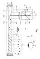
- Example 1 as shown in Figs. 1 and 5A , using the buffer member 162, the light guide plate 121 is supported by the two opposing inner side surfaces of the picture-frame-like support member 161.
- the buffer member 162 supports the light guide plate 121 at two portions, i.e., two of the buffer members 162 respectively cover the longitudinal end portions of the light guide plate 121 (two of the buffer members 162 sandwich therebetween the light guide plate 121).
- two of the buffer members 162 support the light guide plate 121 by respectively being in contact with the longitudinal end surface portions of the light guide plate 121.
- Fig. 2 , 3 , and 5A two of the buffer members 162 support the light guide plate 121 by respectively being in contact with the longitudinal end surface portions of the light guide plate 121.
- Fig. 1 the buffer member 162 supports the light guide plate 121 at two portions, i.e., two of the buffer members 162 respectively cover the longitudinal end portions of the light guide plate 121 (two of the buffer members 162 sandwich therebetween the light guide plate
- the support member 161 is shaped as a whole like a picture frame, and the cross-sectional shape thereof is substantially like a letter of "L".
- two of the buffer members 162 support the light guide plate 121 by respectively being in contact with the longitudinal lower end surface portions of the light guide plate 121.
- four of the buffer members 162 support the light guide plate 121, i.e., two of the buffer members 162 respectively cover (pinch) the longitudinal end portions of the light guide plate 121, and the remaining two buffer members 162 respectively cover (pinch) the transverse center portions of the light guide plate 121.
- four of the buffer members 162 support the light guide plate 121 by respectively covering (pinching) four corners of the light guide plate 121. Still alternatively, as shown in Fig.
- the buffer members 162 support the light guide plate 121, i.e., four of the buffer members 162 respectively cover (pinch) the four corners of the light guide plate 121, and the remaining two buffer members 162 respectively cover (pinch) the transverse center portions of the light guide plate 121.
- the buffer members of Figs. 5B, 5C, and 5D are each a modification example of the buffer member of Fig. 1 , but may each be a modification example of the buffer members of Fig. 2 , 3 , and 4 .
- the buffer members of Figs. 1 , 2 , 3 , 4 , 5A, 5B, 5C, and 5D may be combined for use as appropriate.
- the buffer member 162 may have an elastic modulus lower than that of the light guide plate 121 or 321. Assuming that the light guide plate 121 or 321 has the elastic modulus of 1, the buffer member 162 has the elastic modulus of 5 ⁇ 10 -5 , for example.
- the buffer member 162 is made of resin, and is specifically made of epoxy resin, modified silicone resin, epoxy-modified silicone resin, urethane resin, or others with the thickness of 0.01 mm to 20 mm inclusive (e.g., specifically 5 mm) in the example of Fig. 1 .
- the light guide plate 121 or 321 is made of a transparent glass substrate including soda lime glass and super white glass, an optical glass including quartz glass and BK7, a plastic substrate, a plastic sheet, and a plastic film with the thickness of 0.01 mm to 3 mm inclusive (e.g., specifically 2 mm).
- the support member 161, 171, or 177 may be affixed, on its top surface opposite to a viewer, with a protection member (protection plate) for protecting the light guide plate 121 or 321.
- the image display device 100, 200, 300, or 400 may be attached to the frame fixedly or detachably.
- the optical system 112 or 254 is disposed between the image forming unit 111 or 211 and the light guide unit 120 or 320.
- the luminous flux as a result of collimation by the optical system 112 or 254 is directed into the light guide unit 120 or 320, is guided therein, and is emitted therefrom.
- the light guide unit 120 or 320 is semi-transmissive (see-through type).
- At least a part of the light guide unit facing the eyes of the viewer 20 may be semi-transmissive (see-through), and through such a part of the light guide unit, the viewer may see the outside view.
- Example 1 in a light beam emitted from the center of the image forming unit 111 or 211 and passed through a node in the optical system 112 or 254 on the side of the image forming unit (center light beam CL), a part of the center light beam vertically enters the light guide unit 120 or 320 (at-center incident light beam).
- the point at which the at-center incident light beam enters the light guide unit 120 or 320 is referred to as "light-guide-unit center point O".
- the axis passing through the light-guide-unit center point O, and being parallel to the axis of the light guide unit 120 or 320 is referred to as "X axis", and the axis passing through the light-guide-unit center point O, and coinciding with the normal to the light guide unit 120 or 320 is referred to as "Z axis”.
- the center point of the first deflection section 130 or 330 that will be described next is the light-guide-unit center point O. That is, as shown in Fig.
- the center light beam CL emitted from the center of the image forming unit 111 or 211 and passed through a node in the optical system 112 or 254 on the side of the image forming unit bumps on the light guide plate 121 or 321 in the vertical direction.
- the center light beam CL enters the light guide plate 121 or 321 at an angle of 0 degrees.
- the center of an image to be displayed coincides with the normal to the first plane 122 or 322 of the light guide plate 121 or 321.
- the first and second deflection sections 130 and 140 are both disposed in the light guide plate 121.
- the first deflection section 130 reflects light directed into the light guide plate 121
- the second deflection section 140 passes therethrough and reflects the light for a plurality of times after the light is propagated by total reflection in the light guide plate 121. That is, the first deflection section 130 serves as a reflection mirror, and the second deflection section 140 serves as a semi-transmissive mirror.
- the first deflection section 130 provided in the light guide plate 121 is made of aluminum (Al), and is configured by a light reflection film (a kind of mirror) that reflects the light directed into the light guide plate 121.
- the second deflection section 140 also provided in the light guide plate 121 is configured by a multi-layer film structure of a plurality of dielectric layers.
- the dielectric multi-layer film includes a layer of TiO 2 (titanium dioxide) being a high dielectric material, and a layer of SiO 2 (silicon dioxide) being a low dielectric material.
- TiO 2 titanium dioxide
- SiO 2 silicon dioxide
- the multi-layer film structure of a plurality of dielectric layers is described in Japanese Unexamined Patent Application Publication No. 2005-521099 .
- a dielectric six-layer film is exemplarily shown, but this is not restrictive.
- a dielectric layer and another dielectric layer include therebetween a very thin layer made of the same material as the light guide plate 121.
- the collimated light directed into the light guide plate 121 is reflected (or diffracted) in order to achieve total reflection of the light in the light guide plate 121.
- the collimated light is reflected (or diffracted) for a plurality of times after the light is propagated by total reflection in the light guide plate 121, and remains collimated when it is emitted from the light guide plate 121 toward the eyes 21 of the viewer 20.
- the light guide plate 121 is partially cut out to obtain a sloped surface, i.e., cut-out portion 124, and the resulting sloped surface is provided thereon with a light reflection film, i.e., first deflection section 130, by vapor deposition.
- the cut-out portion 124 is then attached to the first deflection section 130.
- formed is a multi-layer film structure of a plurality of layers made of the same material as the light guide unit 121, e.g., glass, and a plurality of dielectric layers (e.g., formed by vapor deposition).
- the light guide plate 121 is then partially cut out to obtain a sloped surface, i.e., cut-out portion 125, and the resulting sloped surface is provided thereon with the multi-layer structure.
- the resulting structure is then put in shape by abrasion, for example. This obtains the light guide unit 120 including the light guide plate 121 formed therein with the first and second deflection sections 130 and 140.
- the light guide plate 121 or 321 includes two parallel planes (the first plane 122 or 322, and the second plane 123 or 323) extending parallel to the direction of light propagation (X axis) by total reflection in the light guide plate 121 or 321.
- the first plane 122 or 322 and the second plane 123 or 323 are opposed to each other. Collimated light enters the first plane 122 or 322 being the light incident plane, and then exits from the second plane 123 or 323 being the light exit plane after the light is propagated by total reflection in the light guide plate.
- the second plane 123 or 323 may serve as the light incident plane
- the first plane 122 or 322 may serve as the light exit plane.
- the image forming unit 111 is the first image forming unit, and includes a plurality of pixels arranged in a 2D matrix.
- the image forming unit 111 includes a reflective spatial light modulator 150, and a light source 153 configured by a light-emitting diode that emits white light.
- the image forming unit 111 is housed as a whole in a chassis 113 (indicated by alternate long and short dashed lines in Fig. 1 ).
- the chassis 113 is formed with an aperture (not shown), and through this aperture, light is emitted from the optical system 112, i.e., collimator light emitting optical system or collimator optical system.
- the light guide plate 121 is attached to the chassis 113.
- the reflective spatial light modulator 150 is configured by a liquid crystal display (LCD) 151 configured by LCOS as a light bulb, and a polarized beam splitter 152. With the polarized beam splitter 152, light coming from the light source 153 is partially reflected and then is directed to the liquid crystal display 151, and the light reflected by the liquid crystal display 151 is partially passed therethrough and is directed to the optical system 112.
- the liquid crystal display 151 includes a plurality of, e.g., 640 ⁇ 480 pieces of, pixels (liquid crystal cells) arranged in a 2D matrix.
- the polarized beam splitter 152 is in the well-known structure and configuration.
- the not-polarized light coming from the light source 153 bumps on the polarized beam splitter 152.
- the polarized beam splitter 152 passes therethrough any P-polarized components, and emits the components to the outside of the system.
- the polarized beam splitter 152 reflects any S-polarized components.
- the S-polarized components are then directed into the liquid crystal display 151, are reflected therein, and are emitted therefrom.
- light beams emitted from "white” pixels contain a high proportion of P-polarized components
- light beams emitted from "black” pixels contain a high proportion of S-polarized components.
- the P-polarized components pass through the polarized beam splitter 152, and are then guided to the optical system 112.
- the S-polarized components are reflected by the polarized beam splitter 152, and are then put back to the light source 153.
- the optical system 112 is a convex lens, for example, and at the focal length in the optical system 112, the image forming unit 111 (more specifically, the image display device 151) is disposed for generating collimated light.
- the frame 10 is configured by a front section 11, two temple sections 13, and two temple tip sections 14.
- the front section 11 is disposed to be in front of the viewer 20, and the two temple sections 13 are respectively attached to the ends of the front section 11 via hinges 12 to be able to rotate.
- the temple tip sections 14 are also referred to as tip cells or ear pads, and are respectively attached to tip end portions of the temple sections 13.
- the frame 10 is attached also with a nose pad (not shown in Fig. 6 ). That is, the structure including the frame 10 and the nose pad looks substantially the same as that of ordinary glasses. What is more, the temple sections 13 are each attached with the chassis 113 to be detachable by a retention member 19.
- the frame 10 is made of metal or plastic.
- the temple sections 13 may be each attached with the chassis 113 not to be detachable by the retention member 19.
- temple sections of the frame may be each attached with the chassis 113 to be detachable by the retention member 19.
- the chassis 113 may be attached inside or outside of each of the temple sections 13.
- a wiring line (signal line or power supply line) 15 from one image forming unit 111A goes through the temple section 13 and the temple tip section 14 to be outside from the tip end portion of the temple tip section 14, and then is connected to a control unit (control circuit or control section) 18.
- the image forming unit 111A and another image forming unit 111B are each provided with a headphone section 16, and a headphone-use wiring line 16' from each of the image forming units 111A and 111B goes through the temple section 13 and the temple tip section 14 to reach the headphone section 16 via the tip end portion of the temple tip section 14.
- the headphone-use wiring line 16' goes around behind the pinna from the tip end portion of the temple tip section 14, and reaches the headphone section 16.
- Such a configuration simplifies the display apparatus without giving a viewer an impression that the headphone sections 16 and the headphone-use wiring lines 16' do not look tidy.
- the wiring line (signal line or power supply line) 15 is connected to the control unit (control circuit) 18.
- the control unit 18 is provided with an image information storage unit 18A, for example.
- the control unit 18 performs processing for image display.
- the control unit 18 and the image information storage unit 18A may be each configured by a well-known circuit.
- an imaging unit 17 may be attached using any appropriate attachment member (not shown).
- the imaging unit 17 is one configured by a solid-state imaging element being a CCD (Charge-Coupled Device) or a CMOS (Complementary Metal Oxide Semiconductor) sensor, and a lens (these are not shown). Signals from the imaging unit 17 are sent to the image forming unit 111A via a wiring line (not shown) extending from the imaging unit 17, for example.
- control unit (control circuit, control section) 18 provided in the display apparatus is incorporated with a communication unit (receiver), or the display apparatus includes a communication section (receiver) such as mobile phone or smartphone.
- a communication unit such as mobile phone or smartphone.
- information and data relevant to images to be displayed on the image display device may be recorded, retained, and stored in a so-called cloud computer and a server. This allows transmission/reception, and exchange of various types of information and data between the display apparatus and the cloud computer or the server. This also allows reception of signals based on various types of information and data, i.e., signals for image display on the image display device, and allows the receiver to receive the signals.
- the display apparatus When the display apparatus receives the signals for image display on the image display device 100, 200, 300, or 400, e.g., electronic mails and various types of information in a variety of sites on the Internet, the image display device 100, 200, 300, or 400 accordingly displays such electronic mails and various types of information.
- a dimmer unit 700 may be changed in light transmittance under the control of the control unit 18.
- the signals for image display on the image display device 100, 200, 300, or 400 may be stored in the image display device, e.g., specifically in the image information storage unit 18A in the control unit 18.
- the light guide plate is supported by the support member using the buffer member at a plurality of portions.
- Such a configuration prevents, without fail, the degradation problems of display images that are caused by the expanded/contracted light guide plate resulted from an environmental temperature change or a difference of thermal expansion coefficients between the members in the light guide unit.
- the light guide plate may be retained with sufficient stability.
- Example 2 is a modification of Example 1.
- an image forming unit 211 is the second image forming unit. That is, the image forming unit 211 includes a light source 251, and a scanning section 253 that scans collimated light coming from the light source 251.
- the image forming unit 211 includes
- the light source 251 is a light-emitting element that emits white light.
- Light from the light source 251 enters the collimator optical system 252 having the positive optical power as a whole, and is collimated and emitted.
- This collimated light is then reflected by a total-reflection mirror 256, and then is horizontally and vertically scanned by the scanning section 253.
- This scanning section 253 is configured by a MEMS in which a micro mirror is rotatable in the 2D direction so that the collimated light is scanned two-dimensionally.
- a kind of 2D image is then formed, and virtual images are generated (e.g., the number of the pixels is the same as those in Example 1).
- Light from these virtual pixels passes through the relay optical system (collimator light emitting optical system) 254 configured by a well-known relay optical system, and luminous flux being the collimated light enters the light guide unit 120.
- the light guide unit 120 that receives, guides, and emits the luminous flux being the collimated light obtained in the relay optical system 254 is in the same structure and configuration as the light guide unit described in Example 1, and thus is not described in detail again.
- the display apparatus in Example 2 is substantially in the same structure and configuration as the display apparatus in Example 1 except for the image forming unit 211, and thus is not described in detail again.
- Example 3 is also a modification of Example 1.
- Fig. 9 is a conceptual view of the image display device 300 in a display apparatus (head mounted display) in Example 3.
- Fig. 10 is a schematic cross-sectional view of a partially-enlarged reflective volumetric holographic diffraction grating.
- the image forming unit 111 is the first image forming unit similarly in Example 1.
- the light guide unit 320 is basically the same as the light guide unit 120 in Example 1 in terms of structure and configuration except for first and second deflection sections.
- the first and second deflection sections are provided on the surface of the light guide plate 321 (specifically on the second plane 323 of the light guide plate 321).
- the first deflection section diffracts and reflects light directed into the light guide plate 321
- the second deflection section diffracts and reflects the light for a plurality of times after the light is propagated by total reflection in the light guide plate 321.
- the first and second deflection sections are each a diffraction grating element, specifically a reflective diffraction grating element, and more specifically a reflective volumetric holographic grating element.
- first deflection section being a reflective volumetric holographic diffraction grating
- second deflection section being a reflective volumetric holographic diffraction grating
- the first and second diffraction grating members 330 and 340 are each a laminate structure of a single diffraction grating layer.
- the diffraction grating layers are each made of photopolymer, and are each manufactured in the previous manner with an interference pattern formed to correspond to one wavelength band (or wavelength).
- the interference pattern formed on the diffraction grating layer (diffraction optical element) is constant in pitch, and is linear and parallel to the Y axis.
- the axes of the first diffraction grating members 330 and 340 are both parallel to the X axis, and the normals thereto are parallel to the Z axis.
- Fig. 10 is a schematic cross-sectional view of a partially-enlarged reflective volumetric holographic diffraction grating.
- the reflective volumetric holographic diffraction grating is formed with an interference pattern with a desired slant angle of ⁇ .
- the slant angle ⁇ means an angle formed between the surface of the reflective volumetric holographic diffraction grating and the interference pattern.
- the interference pattern is formed from the inside to the surface of the reflective volumetric holographic diffraction grating.
- the interference pattern satisfies Bragg's Law.
- Bragg's Law means a condition satisfying Equation A below.
- Equation A m denotes a positive integer, ⁇ denotes a wavelength, d denotes a grating surface pitch (normal interval on virtual plane including interference pattern), and ⁇ denotes a complementary angle of light entering the interference pattern.
- Equation B shows the relationship between the complementary angle ⁇ , the slant angle ⁇ , and an incident angle ⁇ when light enters the diffraction grating member at the incident angle ⁇ .
- the first diffraction grating member 330 is disposed (attached) on the second plane 323 of the light guide plate 321, and as to collimated light directed into the light guide plate 321 from the first plane 322, diffracts and reflects the light to achieve total reflection thereof in the light guide plate 321.
- the second diffraction grating member 340 is disposed (attached) on the second plane 323 of the light guide plate 321, and diffracts and reflects the collimated light for a plurality of times after the light is propagated by total reflection in the light guide plate 321. The light remains collimated when it is emitted from the first plane 322 of the light guide plate 321.
- the collimated light is emitted after the light is propagated by total reflection therein.
- the light guide plate 321 is thin, and thus an optical path is long for the light to propagate therein. Therefore, the light is reflected a different number of times depending on the viewing angle before reaching the second diffraction grating member 340. More in detail, in the collimated light entering the light guide plate 321, a part of the light entering the light guide plate 321 at an angle in the direction of being closer to the second diffraction grating member 340 is reflected less often than a part of the light entering the light guide plate 321 at an angle in the direction of being away from the second diffraction grating member 340.
- the collimated light entering the light guide plate 321 at an angle in the direction of being closer to the second diffraction grating member 340 forms an angle smaller than the collimated light entering the light guide plate 321 at an angle in the opposite direction.
- This angle is formed with the normal to the light guide plate 321 when the light propagating in the light guide plate 321 bumps on the inner surface thereof.
- the interference patterns formed in the first and second diffraction gating members 330 and 340 are symmetrical with respect to the virtual plane, which is vertical to the axis of the light guide plate 321.
- the light guide plate 321 in Example 4 that will be described later is basically the same as the light guide plate 321 described above in terms of structure and configuration.
- the display apparatus in Example 3 is substantially in the same structure and configuration as the display apparatus in Example 1 except for the light guide unit 320, and thus is not described in detail again.
- Example 4 is a modification of Example 3.
- Fig. 11 is a conceptual view of an image display device in a display apparatus (head mounted display) in Example 4.
- the components in the image display device 400 in Example 4 i.e., the light source 251, the collimator optical system 252, the scanning section 253, the collimator light emitting optical system (relay optical system 254), and others, are in the same structure and configuration as those in Example 2 (the second image forming unit).
- the light guide unit 320 in Example 4 is in the same structure and configuration as the light guide unit 320 in Example 3.
- the display apparatus in Example 4 is substantially in the same structure and configuration as the display apparatus in Example 2, and thus is not described in detail again.
- the light guide unit is configured by a piece of light guide plate.
- first, second, and third light guide plates 321R, 321G, and 321B may be stacked together with an interval thereamong as shown in a conceptual view of Fig. 12 . That is, the first light guide plate 321R is provided with a diffraction grating member (not shown) being a layer of reflective volumetric holographic diffraction grating that diffracts and reflects light in a red wavelength band (or with a red wavelength).
- the second light guide plate 321G is provided with a diffraction grating member (not shown) being a layer of reflective volumetric holographic diffraction grating that diffracts and reflects light in a green wavelength band (or with a green wavelength).
- the third light guide plate 321B is provided with a diffraction grating member (not shown) being a layer of reflective volumetric holographic diffraction grating that diffracts and reflects light in a blue wavelength band (or with a blue wavelength).
- the light guide plate is made of resin with the thickness of 1.0 mm
- the support member 161 is made of magnesium alloy with the thickness of 3.5 mm.
- an adhesive 163 with the thickness of 0.1 mm
- the first and second light guide plates 321R and 321G are bonded together at their end portions
- the second and third light guide plates 321G and 321B are bonded together at their end portions.
- the interval between the first and second light guide plates 321R and 321G is 0.1 mm
- the interval between the second and third light guide plates 321G and 321B is 0.1 mm.
- the buffer member 162 is made of an adhesive material with the thickness of 0.5 mm.
- the light guide plates each have an elastic modulus of 1
- the buffer member 162 and the adhesive 163 respectively have the elastic modulus of 5 ⁇ 10 -5 and 3.5.
- the support member 161 is attached with the three light guide plates 321R, 321G, and 321B at their end portions using not the buffer members 162 but an adhesive same as the adhesive 163, by the same method shown in Fig. 12 .
- the simulation result shows 0.1 for the light guide plate in the light guide unit in Example 4 as the maximum possible value of warping when the maximum possible value of warping is 1 for the light guide plate in the light guide unit in Comparison Example.
- Example 5 is about a display apparatus according to the second embodiment of the present disclosure, an image display device according to the second embodiment of the present disclosure, and a light guide unit according to the second embodiment of the present disclosure.
- Figs. 13A, 13B , 14A, 14C, and 14E are each a schematic plan view of a light guide plate, a support member, and a buffer member, showing the layout thereof in the display apparatus, the image display device, and the light guide unit in Example 5. Note that the remaining components in Example 5 are the same as those in Examples 1 to 4 except for a fixing member, and the conceptual view of the image display device in Example 5 is the same as that of the image display devices in Examples 1 to 4, and thus no detailed description thereabout is given.
- the fixing member 172 is a spring.
- the leaf spring 172 is provided in the example of Fig. 13A .
- Fig. 13B partially shows the light guide plate 121, the support member 171, and the fixing member 172, in the interval between the light guide plate 121 and the support member 171, provided is the meandering spring 172.
- the fixing member 172 is formed with a buffer area 174, and this buffer area is formed with voids or notch sections 174'.
- the fixing member 172 is specifically an adhesive layer (more specifically, is made of epoxy resin, modified silicone resin, epoxy-modified silicone resin, urethane resin, or others), and although not essential, the adhesive layer is formed with the voids or notch sections 174'.
- Fig. 14B shows a schematic plan view of the fixing member 172.
- the light guide plate 121 is provided with a buffer area 176 on the outer circumferential portion thereof. This buffer area 176 is formed with voids or notch sections 176'.
- Fig. 14D shows a schematic plan view of the light guide plate 121. Still alternatively, as shown in Fig. 14E , a buffer area 178 is provided to the inner circumferential portion of the support member 177, and this buffer area 178 is formed with void or notch sections 178'.
- the fixing member 175 or 179 is provided to fix the light guide plate 121 to the support member 171 or 177.
- Fig. 14F shows a schematic plan view of the support member 177.
- the fixing member 172, 173, 175, or 179 attaches the light guide plate 121 to the support member 171 or 177 by being entirely in contact with the outer circumferential portion of the light guide plate 121.
- the fixing member may attach the light guide plate 121 to the support member 171 or 177 by being in contact with at least four portions on the outer circumferential portion of the light guide plate 121, i.e., in contact with at least a portion on each side of the square-shaped light guide plate 121.
- the structures and configurations in Figs. 13A, 13B , 14A, 14C, and 14E may be combined as appropriate.
- the fixing member for use to fix the light guide plate to the support member is disposed therebetween and around the light guide plate.
- Such a configuration prevents, without fail, the degradation problems of display images that are caused by the expanded/contracted light guide plate resulted from an environmental temperature change or a difference of thermal expansion coefficients between the members therein. Also in such a configuration, the light guide plate may be retained with sufficient stability.
- Example 6 is a modification of Examples 1 to 5, and as shown in a conceptual view of Fig. 15 , the light guide plate 121 is attached with the dimmer unit 700 on the second plane side. That is, the dimmer unit 700 is provided on the side of the light guide unit 120 or 320 not provided with the image forming unit 111 or 211. To be specific, using an adhesive 707, the dimmer unit 700 being a kind of optical shutter is fixed to the light guide unit 120 or 320, specifically to a protection member (protection plate) 126 that protects the light guide plate 121 or 321. The dimmer unit 700 is provided to the area of the light guide unit 120 or 320 on the side opposite to the viewer 20.
- a protection member protection plate
- the protection member (protection plate) 126 is attached to the second plane 123 or 323 of the light guide plate 121 or 321 using an adhesive 127, and the protection member (protection plate) 126 covers the first deflection section 130 or 330, and the second deflection section 140 or 340.
- the second deflection section 140 or 340 is positioned in the projection image of the dimmer unit 700. Figs. 15 , 17A , 18A , 19 , 20 , 21 , 22 , 23 , 24 , 25 , 26 , 27 , 28 , 29 , 30 , 31 , and 32 do not show the support member and others.
- the dimmer unit 700 in Example 6 is an optical shutter in which a light-transmission control material layer 705 is made of a liquid crystal material. That is, the dimmer unit 700 includes transparent first and second substrates 701 and 703, the first substrate opposing the light guide unit 120, the second substrate 703 opposing the first substrate 701, first and second electrodes 702 and 704 respectively provided to the first and second substrates 701 and 703, and the light-transmission control material layer 705 sealed between the first and second substrates 701 and 703.
- the first and second substrates 701 and 703 are each made of a plastic material.
- the first and second electrodes 702 and 704 are each a transparent electrode made of ITO (indium tin oxide), and are each formed by a combination of PVD such as sputtering and lifting off.
- the light-transmission control material layer 705 is specifically a liquid crystal layer made of a TN (Twisted Nematic) liquid crystal material.
- the first and second electrodes 702 and 704 are not patterned, and are so-called solid electrodes. However, the first and second electrodes 702 and 704 may be patterned as appropriate.
- the first and second electrodes 702 and 704 are connected to the control unit 18 via connectors and wiring lines that are not shown.
- the first and second substrates 701 and 703 are sealed together at outer edge portions using a sealing agent 706.
- the first substrate 701 of the dimmer unit 700 and the protection member 126 (protecting the light guide plate 121) are attached together by the adhesive 707.
- the first and second substrates 701 and 703 are each affixed with a polarizer film on the outer surface, but these polarizer films are not shown.
- the first substrate 701 in the dimmer unit 700 is shorter than the light guide plate 121, and the first substrate 701 in the dimmer unit 700 is fixed to the protection member 126 using the adhesive 707.
- the adhesive 707 is provided at the outer edge portion of the first substrate 701. This is applicable also to other Examples to be described below.
- the light guide unit 120 and the dimmer unit 700 are disposed in this order from the viewer's side.
- the dimmer unit 700 is controlled in light transmittance by voltage to be applied to the first and second electrodes 702 and 704.
- voltage to be applied to the first electrode 702 while the second electrode 704 is grounded, for example, this causes a change of liquid crystal alignment in the liquid crystal layer configuring the light-transmission control material layer 705 so that the light transmittance is changed in the liquid crystal layer (refer to Figs. 16A and 16B ).
- a viewer may operate a control knob provided to the control unit 18. That is, the viewer may adjust the light transmittance of the dimmer unit 700 while viewing images provided by the light guide unit 120 or 320.
- the image display device offers satisfactory images to the viewer with no disturbance by the outside light.
- the dimmer unit 700 is attached to the image display device 100, i.e., the dimmer unit 700 is specifically attached to the light guide unit 120.
- the dimmer unit 700 may be attached to the frame 10, or to the chassis 113.
- the dimmer unit 700 may be ON at all times, may be operated/not operated (turned ON/OFF) in response to a viewer's command (operation), or may be OFF under normal conditions and may start operating in response to a signal for image display on the image display device 100, 200, 300 or 400.
- the display apparatus may be further provided with a microphone, and may control the operation of the dimmer unit 700 in response to an audio input via the microphone, for example.
- the dimmer unit may be controlled to operate/not to operate in response to a command issued by a viewer's voice.
- the display apparatus may further include an infrared light incident/exit unit, and using this infrared light incident/exit unit, may control the operation of the dimmer unit 700. That is, a viewer's blinking may be detected using the infrared light incident/exit unit to control the dimmer unit 700 to operate/not to operate.
- Example 7 is a modification of Example 6.
- Fig. 17A is a schematic top view of a display apparatus in Example 7
- Fig. 17B is a schematic view of a circuit that controls an illumination sensor.
- the display apparatus in Example 7 is further provided with a sensor 801 that measures the brightness in the outside environment. Based on the measurement result of outside brightness obtained by the sensor (hereinafter referred to as "first illumination sensor" for convenience) 801, a part of the dimmer unit 700 is changed in light transmittance.
- first illumination sensor for convenience
- the display apparatus in Example 7 is further provided with the first illumination sensor (environmental illumination measurement sensor) 801 that measures the illumination in the environment where the display apparatus is disposed.
- the display apparatus controls the light transmittance of the dimmer unit 700 based on the measurement result of the first illumination sensor 801. Together with or separately from the control over the light transmittance, the display apparatus controls the luminance of images to be formed by the image forming unit 111 or 211 based on the measurement result of the first illumination sensor 801.
- the first illumination sensor 801 in the well-known structure and configuration may be provided to the outer end portion of the light guide unit 120 or 320, or to the outer end portion of the dimmer unit.
- the first illumination sensor 801 is connected to the control unit 18 via connectors and wiring lines that are not shown.
- the control unit 18 includes a circuit for controlling the first illumination sensor 801.
- This circuit for controlling the first illumination sensor 801 is configured by an illumination calculation circuit, a comparison calculation circuit, and an environmental illumination measurement sensor control circuit.
- the illumination calculation circuit calculates the illumination based on the measurement value provided by the first illumination sensor 801.
- the comparison calculation circuit compares the calculation result of the illumination calculation circuit, i.e., illumination value, with a standard value.
- the environmental illumination measurement sensor control circuit controls the dimmer unit 700 and/or the image forming unit 111 or 211 based on the value obtained by the comparison calculation circuit. These circuits may be each a well-known circuit.
- the control over the light transmittance in the dimmer unit 700 and the control over the luminance of images formed by the image forming unit 111 or 211 may be executed separately or executed in correlation with each other.
- the dimmer unit 700 is adjusted to have the light transmittance of a predetermined value (first light transmittance) or lower.
- first illumination measurement value 10 lux
- second illumination measurement value the first light transmittance takes any value in a range from 1% to 30% inclusive
- the second illumination measurement value is 0.01 lux
- the second light transmittance takes any value in a range from 51% to 99% inclusive, for example.
- the first illumination sensor 801 in Example 7 is applicable to the display apparatuses described in Examples 2 to 5.
- the first illumination sensor 801 may be configured by light-receiving elements provided to the imaging unit for exposure measurement.
- the light transmittance of the dimmer unit is controlled based on the measurement result of the first illumination sensor (environmental illumination measurement sensor), and the luminance of images to be formed by the image forming unit is controlled also based on the measurement result of the first illumination sensor.
- the light transmittance of the dimmer unit is controlled based on the measurement result of the second illumination sensor (transmitted-light illumination measurement sensor), and the luminance of images to be formed by the image forming unit is controlled also based on the measurement result of the second illumination sensor.
- Such control execution offers high-contrast images for viewing by a viewer, and also optimizes the surrounding conditions for viewer's image viewing considering the illumination in the ambient environment where the display apparatus is disposed.
- Example 8 is also a modification of Example 6.
- Fig. 18A is a schematic top view of a display apparatus in Example 8
- Fig. 18B is a schematic view of a circuit that controls an illumination sensor.
- the display apparatus in Example 8 measures the illumination based on light passed through the dimmer unit from the outside environment. That is, the display apparatus is further provided with a second illumination sensor (transmitted-light illumination measurement sensor) 802 that measures the illumination of environment light, i.e., whether the light is adjusted to have a desired value of illumination after passing through the dimmer unit.
- the measurement result of the second illumination sensor 802 is used as a basis to control the light transmittance of the dimmer unit 700.
- the display apparatus controls the luminance of images to be formed by the image forming unit 111 or 211 based on the measurement result of the second illumination sensor 802.
- the second illumination sensor 802 in the well-known structure and configuration is provided closer to the viewer's side than the light guide unit 120 or 320.
- the second illumination sensor 802 may be provided to the surface of the light guide unit 121 or 321 on the viewer's side.
- the second illumination sensor 802 is connected to the control unit 18 via connectors and wiring lines that are not shown.
- the control unit 18 includes a circuit for controlling the second illumination sensor 802.
- This circuit for controlling the second illumination sensor 802 is configured by an illumination calculation circuit, a comparison calculation circuit, and a transmitted-light illumination measurement sensor control circuit.
- the illumination calculation circuit calculates the illumination based on the measurement value provided by the second illumination sensor 802.
- the comparison calculation circuit compares the calculation result of the illumination calculation circuit, i.e., illumination value, with a standard value.
- the transmitted-light illumination measurement sensor control circuit controls the dimmer unit 700 and/or the image forming unit 111 or 211 based on the value obtained by the comparison calculation circuit. These circuits may be each a well-known circuit.
- the control over the light transmittance in the dimmer unit 700 and the control over the luminance of images formed by the image forming unit 111 or 211 may be executed separately or executed in correlation with each other.
- the dimmer unit may be adjusted in light transmittance at the same time with value monitoring of the second illumination sensor 802.
- the second illumination sensor (transmitted-light illumination measurement sensor) 802 in Example 8 is applicable to the display apparatuses described in Examples 2 to 5.
- the second illumination sensor 802 in Example 8 may be combined with the first illumination sensor 801 in Example 7 for use. If this is the case, with various tests, the control over the light transmittance in the dimmer unit 700 may be executed separately from or in correlation with the control over the luminance of images to be formed by the image forming unit 111 or 211.
- Example 9 is a modification of Examples 1 to 8, and is about the display apparatus in the second embodiment.
- Fig. 19 is a conceptual view of an image display device in Example 9
- Fig. 20 is a schematic top view of the display apparatus (specifically head mounted display (HMD)) in Example 9.
- HMD head mounted display
- a light shielding member 710 is provided to an area of the light guide unit 120 where light comes from the image forming unit 111A or 111B, specifically to an area where the first deflection section 130 is provided.
- This light shielding member 710 is for shielding the light guide unit 120 from the outside light.
- the projection image of the light shielding member 710 toward the light guide unit 120 includes the area of the light guide unit 120 where the light comes from the image forming unit 111A or 111B.
- the projection image of the light shielding member 710 toward the light guide unit 120 also includes the projection image of the end portion of the dimmer unit 700 toward the light guide unit 120.
- the light shielding member 710 is provided to the light guide unit 120 on the side not provided with the image forming unit 111A or 111B, and is provided with a distance from the light guide unit 120.
- the light shielding member 710 is made of a non-transparent plastic material, for example.
- This light shielding member 710 is integrally extended from the chassis of the image display device 111A or 111B, or is attached to the chassis 113 of the image forming unit 111A or 111B, or is integrally extended from the frame 10, or is attached to the frame 10.
- the light shielding member 710 is integrally extended from the chassis 113 of the image forming unit 111A or 111B.
- the light shielding member is provided to an area of the light guide unit where light comes from the image forming unit.
- This light shielding member is for shielding the light guide unit from the outside light. Therefore, even if the operation of the dimmer unit changes the amount of incoming outside light, this does not cause image degradation on the display apparatus with no undesired stray light because no outside light enters the area of the light guide unit where light comes from the image forming unit, i.e., the first deflection section 130, in the first place.
- Example 10 is a modification of Example 9. As shown in a conceptual view of Fig. 21 , unlike the display apparatus in Example 9, a display apparatus in Example 10 includes a light shielding member 720 in a portion of the light guide unit 120 on the side not provided with the image forming unit 111A or 111B. To be specific, the light shielding member 720 may be formed with printing on the light guide unit 120 (specifically on the inner surface of the protection member 126) using a non-transparent ink. Other than that, the display apparatus in Example 10 is in the same structure and configuration as the display apparatus in Example 9, and thus is not described in detail again. The light shielding member 720 in Example 10 may be combined with the light shielding member 710 in Example 9 for use. The light shielding member 720 may be formed on the outer surface of the protection member 126.
- Example 11 is also a modification of Example 9. As shown in a conceptual view of Fig. 22 or 23 , unlike the display apparatuses in Examples 9 and 10, a display apparatus in Example 11 includes a light shielding member 730 in the dimmer unit 700.
- the light shielding member 730 may be formed with printing on the dimmer unit 700 using a non-transparent ink.
- the light shielding member 730 is formed on the outer surface of the first substrate 701 in the dimmer unit 700
- the light shielding member 730 is formed on the inner surface of the first substrate 701 in the dimmer unit 700.
- the display apparatus in Example 11 is in the same structure and configuration as the display apparatus in Example 9, and thus is not described in detail again.
- the light shielding member 730 in Example 11 may be combined with the light shielding member 710 in Example 9 for use, the light shielding member 730 in Example 11 may be combined with the light shielding member 720 in Example 10 for use, or the light shielding member 730 in Example 11 may be combined with the light shielding members 710 and 720 in Examples 9 and 10.
- Example 12 is a modification of Examples 6 to 11.
- the light-transmission control material layer 705 is configured by a liquid crystal material layer.
- a light-transmission control material layer 705' is an optical shutter being an inorganic EL material layer.
- the inorganic EL material layer is made of tungstic oxide (WO 3 ).
- first and second substrates 701' and 703' are each a transparent glass substrate such as soda lime glass or super white glass, and the second substrate 703' is made thinner than the first substrate 701'.
- the second substrate 703' is formed with the thickness of 0.2 mm
- the first substrate 701' is formed with the thickness of 0.4 mm.
- the display apparatus in Example 12 is in the same structure and configuration as the display apparatuses in Examples 6 to 12, and thus is not described in detail again.
- the first substrate 701' in the dimmer unit 700' is attached with the protection member 126 using the adhesive 707 similarly to Example 9.
- Example 13 is a modification of Examples 6 to 12, and is about the display apparatus in the first embodiment.
- a dimmer unit 700" includes first and second substrates 701" and 703", the first substrate 701" opposing the light guide unit 120, the second substrate 703" opposing the first substrate 701", electrodes 702" and 704" respectively provided to the first and second substrates 701" and 703", and a light-transmission control material layer 705" sealed between the first and second substrates 701" and 703".
- the first substrate 701" serves also as the component (specifically the protection member 126) in the light guide unit 120. That is, the first substrate 701" and the protection member 126 are the one specific member, and are for shared use.
- the first substrate 701" in the dimmer unit 700" serves also as the component (the protection member 126) in the light guide unit 120. This reduces the entire weight of the display apparatus so that this does not cause discomfort to a user of the display apparatus.
- the display apparatus in Example 13 is in the same structure and configuration as the display apparatuses in Examples 6 to 12, and thus is not described in detail again.
- the light shielding member in the display apparatus in Example 13 is in the same structure and configuration as the dimmer unit in the display apparatuses in Examples 6 to 11, and thus is not described again.
- Example 14 is a modification of Examples 1 to 13.
- Fig. 26 is a schematic front view of a head mounted display in Example 14, and
- Fig. 27 is another schematic front view of the head mounted display in Example 14, i.e., the head mounted display with no frame.
- Fig. 28 is a schematic top view of the head mounted display in Example 14, and
- Fig. 29 is a top view of the head mounted display in Example 14 when the display is mounted on the head portion of the viewer 20.
- Fig. 29 shows only the image display device, and no frame is shown. In the description below, the image display device 100 is mainly described, but the image display devices 200, 300, and 400 are surely also applicable.
- the support members 161, 171, and 177 (and the dimmer unit 700 in some cases) are not shown.
- the head mounted display in Example 14 is further provided with a coupling member 180 to couple together the two image display devices 100.
- the coupling member 180 is attached to a center portion 10C of the frame 10 on the side facing the viewer, i.e., between the viewer 20 and the frame 10, by using a screw (not shown), for example.
- the frame 10 is positioned between the two eyes 21 of the viewer 20.
- the projection image of the coupling member 180 is in the projection image of the frame 10. That is, when the head mounted display is viewed from the front of the viewer 20, the coupling member 180 is not visible as is hidden behind the frame 10.
- the image forming units 111A and 111B are each housed in the chassis 113, and at each end portion of the coupling member 180, the chassis 113 is attached to be adjustable.
- the image forming units 111A and 111B are positioned outside of the eyes 21 of the viewer 20.
- ⁇ denotes a distance from the attachment center 111A C for one of the image forming units 111A to one end portion (one endpiece) 10A of the frame
- ⁇ denotes a distance from the center 180 C of the coupling member 180 to the one end portion (the one endpiece) 10A of the frame
- ⁇ denotes a distance from the attachment center 111B C for the remaining image forming unit 111B to the one end portion (the one endpiece) 10A of the frame
- L denotes a length of the frame 10.
- the image forming units (specifically the image forming units 111A and 111B) to the end portions of the coupling member 180, specifically, three through holes (not shown) are formed to each end portion of the coupling member, and tapped-hole sections (screw sections, not shown) corresponding to these through holes are formed to each of the image forming units 111A and 111B. Thereafter, screws (not shown) are fastened into the hole sections formed to the image forming units 111A and 111B through the through holes. Between each of the screws and each of the hole sections, a spring is inserted in advance.
- the image forming units may be adjusted in state of attachment, i.e., adjusted in angle with respect to the coupling member. After such attachment, the screws are each hidden using a lid (not shown).
- the coupling member 180 and a coupling member 190 are both shaded for explicit indication thereof.
- the coupling member 180 is attached to the center portion 10C of the frame 10, which is positioned between the two eyes 21 of the viewer 20. This center portion 10C corresponds to a bridge section of ordinary glasses.
- a nose pad 10' is attached on the side of the coupling member 180 facing the viewer 20, a nose pad 10' is attached.
- Figs. 28 and 32 do not show the nose pad 10'.
- the frame 10 and the coupling member 180 are each made of metal or plastic, and the coupling member 180 is shaped like a bent rod.
- the coupling member 180 couples together the two image display devices 100, and this coupling member 180 is attached to the center portion 10C of the frame 10 that is positioned between the two eyes 21 of the viewer 20. That is, the image display devices 100 are not directly attached to the frame 10. Therefore, the temple sections 13 are extended outward when the viewer 20 wears the frame 10 on his head portion. As a result, even if the frame 10 is deformed, such deformation of the frame 10 does not cause displacement (position change) of the image forming units 111A and 111B, and even if such displacement occurs, the displacement is negligible. Such a configuration thus prevents a change of convergence angle between right and left images without fail.
- the configuration eliminates having to increase the rigidity of the front section 11 of the frame 10 so that the frame 10 is not increased in weight, the design ability is not impaired, and the cost is not increased. Still further, with the image display devices 100 not directly attached to the eyeglass-shaped frame 10, the frame 10 may be in various designs and colors to meet the viewer's preferences, and the designing of the frame 10 is less restricted and highly flexible. What is more, the coupling member 180 is hidden behind the frame 10 when the head mounted display is viewed from the front of the viewer. This offers the head mounted display with sophistication and refinement of design.
- Example 15 is a modification of Example 14.
- Fig. 30 is a schematic front view of a head mounted display in Example 15, and
- Fig. 31 is another schematic front view of the display apparatus in Example 15, i.e., the head mounted display with no frame.
- Fig. 32 is a schematic top view of the head mounted display in Example 15.
- the rod-like coupling member 190 does not couple the two image forming units 111A and 111B but the two light guide units 120.
- the two light guide units 120 may be integrally manufactured, and the resulting integrally-manufactured light guide unit 120 may be provided with the coupling member 190.
- the coupling member 190 is attached to the center portion 10C of the frame 10 positioned between the two eyes 21 of the viewer 20.
- the image forming units 111 are positioned outside of the eyes 21 of the viewer 20.
- the image forming units 111 are each attached to the end portion of the light guide unit 120.
- Example 15 the frame 10 and the image display devices are in the same structure and configuration as the frame 10 and the image display devices described in Example 14, and thus are not described in detail again.
- the head mounted display in Example 15 is also substantially in the same structure and configuration as the head mounted display in Example 14 except for the above-mentioned difference, and thus is not described in detail again.
- the light guide plate may be provided with a surface relief hologram (refer to United States Patent No. 20040062505A1 ).
- the diffraction grating element may be a transmissive diffraction grating element, or the first or second deflection section may be a reflective diffraction grating element, and the remaining may be a transmissive diffraction grating element.
- the diffraction grating element may be a reflective blazed diffraction grating element.
- the dimmer unit is not used but only the light shielding member may be provided.
- the light guide unit, the image display device, and the display apparatus in the first embodiment of the present disclosure may be combined with those in the second embodiment of the present disclosure.
- the image forming unit 111 or 211 is described to offer image display in a color, e.g., green.
- the image forming unit 111 or 211 may offer color image display.
- the light source may be so configured as to emit light in red, green, and blue, for example.
- the light emitted from red, green, and blue light-emitting elements, i.e., red, green, and blue light may be mixed and made uniform in luminance using a light bulb to obtain white light.
- the dimmer unit may be detachably provided in an area from which the light guide unit emits light.
- the dimmer unit may be attached to the light guide unit using a screw made of transparent plastic, for example.
- the dimmer unit may be then connected to a control circuit via connectors and wiring lines. This control circuit is for controlling the light transmittance of the dimmer unit, and is provided in the control unit 18 that controls the image forming unit, for example.
- an optical shutter for use may be configured by application of electrodeposition/dissociation that occurs in response to the reversible oxidation reduction of metal, e.g., silver particles.
- metal e.g., silver particles.
- Ag + (silver) and I - (iodine) are dissolved in advance in an organic solvent, and Ag is precipitated by reduction of Ag + through appropriate voltage application to electrodes so that the dimmer unit is reduced in light transmittance.
- an optical shutter for use may be configured by utilizing color change of substance that occurs in response to the oxidation reduction of an electrochromic material.
- first and second electrodes are provided, and first and second electrochromic material layers are sandwiched between the first and second electrodes.
- the first electrochromic material layer is configured by a prussian blue metal complex
- the second electrochromic material layer is configured by a nickel-substituted prussian blue metal complex.
- an optical shutter for use may be configured by controlling the light transmittance by electrowetting.
- first and second electrodes are provided, and an insulating first liquid and a conductive second liquid are filled between the first and second electrodes. By voltage application between the first and second electrodes, the interface between the first and second liquids is changed in shape, e.g., from being flat to being bent, thereby controlling the light transmittance.
- the image forming unit or the light source configured by light-emitting elements and a light bulb the following is also possible other than the combination of a backlight emitting white light as a whole and a liquid crystal display including red, green, and blue light-emitting pixels, for example.
- an active-matrix image forming unit is also possible as in a conceptual view of Fig. 33 , for example, i.e., the unit includes a light-emitting panel in which light-emitting elements 601 being semiconductor laser elements are arranged in a 2D matrix, and the light-emitting elements 601 are each controlled to emit/not to emit light. Such control allows direct perception of light emission in the light-emitting elements 601, thereby images are displayed.
- the light emitted from this image forming unit is directed into the light guide plate 121 via the collimator optical system 112.
- the light-emitting elements are semiconductor laser elements.
- a color-display image forming unit in a conceptual view of Fig. 34 is also possible.
- This image forming unit includes
- This color-display image forming unit controls light-emission/no light-emission of the red, green, and blue light-emitting elements 601R, 601G, and 601B.
- the light emitted from this image forming unit is also directed into the light guide plate 121 via the collimator optical system 112.
- a reference numeral 612 denotes a micro lens for gathering the light coming from the light-emitting elements.
- Fig. 35 is a conceptual view of an image forming unit configured by the light-emitting panels 611R, 611G, 611B, and others in which the light-emitting elements 601R, 601G, and 601B are each arranged in a 2D matrix.
- the light emitted from the light-emitting panels 611R, 611G, 611B is controlled by light-pass control units 604R, 604G, and 604B in terms of light-pass/no light-pass.
- the light then enters the dichroic prism 603, is collectively directed to a single optical path, and is then directed into the light guide plate 121 via the collimator optical system 112.
- Fig. 36 is a conceptual view of the image forming unit configured by the light-emitting panels 611R, 611G, 611B, and others in which the light-emitting elements 601R, 601G, and 601B are each arranged in a 2D matrix.
- the light emitted from the light-emitting panels 611R, 611G, 611B enters the dichroic prism 603, and is collectively directed to a single optical path.
- the light from the dichroic prism 603 is then controlled by the light-pass control units 604 in terms of light-pass/no light-pass, and is directed into the light guide plate 121 via the collimator optical system 112.
- This image forming unit includes the light-emitting elements 601R emitting red light, a light-pass control unit being a light bulb for controlling light-pass/no light-pass of the light emitted from the red light-emitting elements 601R, e.g., liquid crystal display 604R, the light-emitting elements 601G emitting green light, a light-pass control unit being a light bulb for controlling light-pass/no light-pass of the light emitted from the green light-emitting elements 601G, e.g., liquid crystal display 604G, the light-emitting elements 601B emitting blue light, and a light-pass control unit being a light bulb for controlling light-pass/no light-pass of the light emitted from the blue light-emitting elements 601B, e.g., liquid crystal display 604B.
- the image forming unit also includes a light directing member 602 configured to guide the light emitted from the light-emitting elements 601R, 601G, and 601B, and a section configured to collectively direct the light to a single optical path, e.g., dichroic prism 603.
- the light emitted from the dichroic prism 603 is directed into the light guide plate 121 via the collimator optical system 112.
- the present disclosure may be also in the following structures.
Landscapes
- Physics & Mathematics (AREA)
- General Physics & Mathematics (AREA)
- Optics & Photonics (AREA)
- Planar Illumination Modules (AREA)
- Electrophotography Configuration And Component (AREA)
- Light Guides In General And Applications Therefor (AREA)
- Diffracting Gratings Or Hologram Optical Elements (AREA)
Abstract
Description
- The present disclosure relates to a light guide unit, image display device, and display apparatus.
- Japanese Patent Application Laid-Open No.
2006-162767 - This
image display device 1100 includes, as shown in the conceptual view ofFig. 38 , animage forming unit 111, a collimatoroptical system 112, and alight guide section 120. Theimage forming unit 111 includes a plurality of pixels that are arranged in a 2D matrix. The collimatoroptical system 112 collimates light coming from each of the pixels in theimage forming unit 111. Thelight guide section 120 guides and emits the resulting collimated light coming from the collimatoroptical system 112. The light emitted from thelight guide section 120 is then guided toeyes 21 of aviewer 20. Thelight guide section 120 is configured by alight guide plate 121, and first andsecond deflection sections light guide plate 121 propagates therein the incoming light by total reflection, and then emits the light. Thefirst deflection section 130 is a single-layer light reflection film, for example, and reflects the light entered thelight guide plate 121 so as to achieve total reflection therein. Thesecond deflection section 140 is a multi-layer light reflection film in the multi-layer film structure, and emits the light from thelight guide plate 121 after the light is propagated therein by total reflection. If such animage display device 1100 configures an HMD, for example, the resulting display apparatus may be reduced in weight and size. - As another virtual image display device well known to provide, for viewing by a viewer, 2D images formed by an image forming unit as enlarged virtual images by an image forming unit, Japanese Patent Application Laid-Open No.
2007-094175 - This
image display device 1300 basically includes, as shown in the conceptual view ofFig. 39 , theimage forming unit 111 that displays images, the collimatoroptical system 112, and alight guide section 320. In thelight guide section 320, light coming from theimage forming unit 111 is guided to theeyes 21 of theviewer 20. Such alight guide section 320 includes alight guide plate 321, and first and second diffraction gratingmembers members light guide plate 321. Collimated light from the collimatoroptical system 112 enters afirst plane 322 of thelight guide plate 321, and then is emitted from thefirst plane 322. Thelight guide plate 321 has asecond plane 323, which is parallel to thefirst plane 322 thereof. Thesecond plane 323 is attached with the first and second diffraction gratingmembers - Such image display devices as above, however, have degradation problems of display images to be viewed by a viewer, e.g., pixel displacement in images or deformed images, due to deviation of light caused by the light being guided by the expanded/contracted light guide plate. The expansion/contraction of the light guide plate is resulted from a temperature difference between the outside air and the viewer's body when the light guide plate is exposed to the outside air, or a transient change of temperature when the viewer moves in/out from a room, for example. A difference of thermal expansion coefficients between the members in the light guide section is also a cause. As an example, Japanese Patent Application Laid-Open No.
2010-087560 - It is thus desirable to provide a light guide unit configured to prevent, without fail, the degradation problems of display images, which are caused by the expanded/contracted light guide plate resulted from an environmental temperature change or a difference of thermal expansion coefficients between the members therein. It is also desirable to provide an image display device including such a light guide unit, and a display apparatus including such an image display device.
- Various respective aspects and features of the invention are defined in the appended claims. Combinations of features from the dependent claims may be combined with features of the independent claims as appropriate and not merely as explicitly set out in the claims.
- In particular some embodiments relate to a display apparatus and, more specifically, to a display apparatus for use as a head mounted display (HMD), for example, and also to an image display device suitable for use in the display apparatus, and a light guide unit suitable for use in the image display device.
- In some embodiments, an image display device is provided, comprising: an image forming unit; and a light guide unit, the light guide unit including a light guide plate configured to guide light of an image formed in the image forming unit, and a support member, the light guide plate being supported by one or more buffer members at, at least, a plurality of portions of the support member.
- In some embodiments, an image display device is provided, comprising: an image forming unit; and a light guide unit, the light guide unit including a light guide plate configured to guide light of an image formed in the image forming unit, and a support member, the light guide plate and the support member including therebetween a fixing member, the fixing member being provided around the light guide plate to fix the light guide plate to the support member.
- In some embodiments, a light guide unit is provided, comprising: a light guide plate; and a support member, the light guide plate being supported by one or more buffer members, the one or more buffer members supporting the light guide plate at, at least, a plurality of portions of the support member.
- In some embodiments, a light guide unit is provided, comprising: a light guide plate; and a support member, the light guide plate and the support member including therebetween a fixing member, the fixing member being provided around the light guide plate to fix the light guide plate to the support member.
- In some embodiments, a display apparatus is provided, comprising: a frame; and an image display device attached to the frame, the image display device including an image forming unit, and a light guide unit, the light guide unit including a light guide plate configured to guide light of an image formed in the image forming unit, and a support member, the light guide plate being supported by one or more buffer members, the one or more buffer members supporting the light guide plate at, at least, a plurality of portions of the support member.
- In some embodiments, a display apparatus is provided, comprising: a frame; and an image display device attached to the frame, the image display device including an image forming unit, and a light guide unit, the light guide unit including a light guide plate configured to guide light of an image formed in the image forming unit, and a support member, the light guide plate and the support member including therebetween a fixing member, the fixing member being provided around the light guide plate to fix the light guide plate to the support member.
- According to a first embodiment of the present disclosure, there is provided a light guide unit including a light guide plate, and a support member, the light guide plate being supported by a buffer member at a plurality of portions of the support member.
- According to a second embodiment of the present disclosure, there is provided a light guide unit including a light guide plate, and a support member, the light guide plate and the support member including therebetween a fixing member, the fixing member being provided around the light guide plate to fix the light guide plate to the support member.
- According to the first or second embodiment of the present disclosure, there is provided an image display device, including an image forming unit, and a light guide unit, the light guide unit including a light guide plate, and a support member, the light guide plate being configured to guide light of an image formed in the image forming unit. In the image display device according to the first embodiment of the present disclosure, the light guide plate is supported by a buffer member at a plurality of portions of the support member. In the image display device according to the second embodiment of the present disclosure, the light guide plate and the support member include therebetween the fixing member, the fixing member being provided around the light guide plate to fix the light guide plate to the support member.
- According to the first or second embodiment of the present disclosure, there is provided a display apparatus, including a frame configured to be mounted on a viewer's head portion, and an image display device attached to the frame, the image display device including an image forming unit, and a light guide unit, the light guide unit including a light guide plate configured to guide light of an image formed in the image forming unit, and a support member.
- In the display apparatus according to the first embodiment of the present disclosure, the light guide plate is supported by a buffer member at a plurality of portions of the support member. In the display apparatus according to the second embodiment of the present disclosure, the light guide plate and the support member include therebetween a fixing member, the fixing member being provided around the light guide plate to fix the light guide plate to the support member.
- In the light guide unit, the image display device, or the display apparatus in the first embodiment of the present disclosure, the light guide plate is supported by the support member using the buffer member at a plurality of portions. Such a configuration can prevent, without fail, the degradation problems of display images that are caused by the expanded/contracted light guide plate resulted from an environmental temperature change or a difference of thermal expansion coefficients between the members in the light guide unit. Such a configuration also can retain the light guide plate with sufficient stability. Moreover, in the light guide unit, the image display device, or the display apparatus in the second embodiment of the present disclosure, the fixing member for use to fix the light guide plate to the support member is disposed therebetween and around the light guide plate. Such a configuration can prevent, without fail, the degradation problems of display images that are caused by the expanded/contracted light guide plate resulted from an environmental temperature change or a difference of thermal expansion coefficient between the members in the light guide unit. Such a configuration also can retain the light guide plate with sufficient stability. Note that the effects described in this Specification are by way of example only and in no way restrictive, and any additional effects are to be applied.
- These and other objects, features and advantages of the present disclosure will become more apparent in light of the following detailed description of best mode embodiments thereof, as illustrated in the accompanying drawings.
- Embodiments of the invention will now be described with reference to the accompanying drawings, throughout which like parts are referred to by like references, and in which:
-
Fig. 1 is a conceptual view of an image display device in a display apparatus in Example 1; -
Fig. 2 is a conceptual view of a modification of the image display device in the display apparatus in Example 1; -
Fig. 3 is a conceptual view of another modification of the image display device in the display apparatus in Example 1; -
Fig. 4 is a conceptual view of still another modification of image display device in the display apparatus in Example 1; -
Figs. 5A, 5B, 5C, and 5D are each a schematic plan view of a light guide plate, a support member, and a buffer member, showing the layout thereof in still another modification of the image display device in the display apparatus in Example 1; -
Fig. 6 is a schematic top view of the display apparatus in Example 1; -
Fig. 7A is a schematic side view of the display apparatus in Example 1, andFig. 7B is a diagram schematically showing propagation of light in a light guide plate in the image display device; -
Fig. 8 is a conceptual view of an image display device in a display apparatus in Example 2; -
Fig. 9 is a conceptual view of an image display device in a display apparatus in Example 3; -
Fig. 10 is a schematic cross-sectional view of a partially-enlarged reflective volumetric holographic diffraction grating in the display apparatus in Example 3; -
Fig. 11 is a conceptual view of an image display device in a display apparatus in Example 4; -
Fig. 12 is a conceptual view of a modification of the image display device in the display apparatus in Example 4; -
Figs. 13A and 13B are each a schematic plan view of a light guide plate, a support member, and a fixing member, showing the layout thereof in an image display device in an image display apparatus in Example 5; -
Figs 14A, 14C, and 14E are each a schematic plan view of a light guide plate, a support member, and a buffer member, showing the layout thereof in a modification of the image display device in the display apparatus in Example 5,Fig. 14B is a schematic plan view of the fixing member,Fig. 14D is a schematic plan view of the light guide plate, andFig. 14F is a schematic plan view of the support member; -
Fig. 15 is a conceptual view of an image display device in a display apparatus in Example 6; -
Figs. 16A and 16B are each a schematic cross-sectional view of a dimmer unit, showing how the dimmer unit operates in the display apparatus in Example 6; -
Fig. 17A is a schematic top view of a display apparatus in Example 7, andFig. 17B is a schematic view of a circuit that controls an illumination sensor; -
Fig. 18A is a schematic top view of a display apparatus in Example 8, andFig. 18B is a schematic view of a circuit that controls an illumination sensor; -
Fig. 19 is a conceptual view of an image display device in a display apparatus in Example 9; -
Fig. 20 is a schematic top view of the display apparatus in Example 9; -
Fig. 21 is a conceptual view of an image display device in a display apparatus in Example 10; -
Fig. 22 is a conceptual view of an image display device in a display apparatus in Example 11; -
Fig. 23 is a conceptual view of a modification of the image display device in the display apparatus in Example 11; -
Fig. 24 is a conceptual view of an image display device in a display apparatus in Example 12; -
Fig. 25 is a conceptual view of an image display device in a display apparatus in Example 13; -
Fig. 26 is a schematic front view of a display apparatus in Example 14; -
Fig. 27 is another schematic front view of the display apparatus in Example 14, i.e., the display apparatus with no frame; -
Fig. 28 is a schematic top view of the display apparatus in Example 14; -
Fig. 29 is a top view of the display apparatus in Example 14 when the apparatus is mounted on a viewer's head portion (only an image display device is shown, and no frame is shown); -
Fig. 30 is a schematic front view of a display apparatus in Example 15; -
Fig. 31 is another schematic front view of the display apparatus in Example 15, i.e., the display apparatus with no frame; -
Fig. 32 is a schematic top view of the display apparatus in Example 15; -
Fig. 33 is a conceptual view of an image forming unit; -
Fig. 34 is a conceptual view of a modification of the image forming unit; -
Fig. 35 is a conceptual view of another modification of the image forming unit; -
Fig. 36 is a conceptual view of still another modification of the image forming unit; -
Fig. 37 is a conceptual view of still another modification of the image forming unit; -
Fig. 38 is a conceptual view of a previous image display device; and -
Fig. 39 is a conceptual view of another previous image display device in a different configuration from the image display device ofFig. 38 . - Hereinafter, Examples of the present disclosure will be described with reference to the drawings. The present disclosure is not restricted to Examples, and various numeric values and materials in Examples are illustrative and not restrictive. The description is given in the following order.
- 1. Description about Light Guide Unit, Image Display Device, and Display Apparatus according to First and Second Embodiments of Present Disclosure, and Overall Description
- 2. Example 1 (Light Guide Unit, Image Display Device, and Display Apparatus according to First Embodiment of Present Disclosure)
- 3. Example 2 (Modification of Example 1)
- 4. Example 3 (Another Modification of Example 1)
- 5. Example 4 (Modification of Example 3)
- 6. Example 5 (Light Guide Unit, Image Display Device and Display Apparatus according to Second Embodiment of Present Disclosure)
- 7. Example 6 (Modification of Examples 1 to 5)
- 8. Example 7 (Modification of Example 6)
- 9. Example 8 (Another Modification of Example 6)
- 10. Example 9 (Modification of Examples 1 to 8)
- 11. Example 10 (Modification of Example 9)
- 12. Example 11 (Another Modification of Example 9)
- 13. Example 12 (Modification of Examples 6 to 11)
- 14. Example 13 (Modification of Examples 6 to 12)
- 15. Example 14 (Modification of Examples 1 to 13)
- 16. Example 15 (Modification of Example 14), and Others [Description about Light Guide Unit, Image Display Device and Display Apparatus according to First and Second Embodiments of Present Disclosure, and Overall Description]
- In the below, the expression of "light guide unit or others in the first embodiment of the present disclosure" means a light guide unit in a first embodiment of the present disclosure, a light guide unit in an image display device in the first embodiment of the present disclosure, and a light guide unit in a display apparatus in the first embodiment of the present disclosure. Moreover, the expression of "light guide unit or others in the second embodiment of the present disclosure" means a light guide unit in a second embodiment of the present disclosure, a light guide unit in an image display device in the second embodiment of the present disclosure, and a light guide unit in a display apparatus in the second embodiment of the present disclosure.
- In the light guide unit or others in the first embodiment of the present disclosure, desirably, using a buffer member, a light guide plate is supported at a plurality of portions of a support member opposed to each other with the light guide plate being sandwiched therebetween. In such a light guide unit or others in the first embodiment of the present disclosure, the buffer member may have an elastic modulus lower than that of the light guide plate. Further, in such a desirable light guide unit or others in the first embodiment of the present disclosure, the buffer member may be made of resin. Still further, also in such a desirable light guide unit or others in the first embodiment of the present disclosure, the support member may be shaped like a picture frame to be around the light guide plate. The resin for the buffer member is specifically exemplified by epoxy resin, modified silicone resin, epoxy-modified silicone resin, or urethane resin. However, these examples are not restrictive, and the buffer member may also be made of a porous material, specifically including porous alumina, porous silicon carbide, porous carbon, sintered porous plastic media, and others, or silica aerogel.
- In the light guide unit or others in the second embodiment of the present disclosure, a fixing member may be provided with a buffer area. If this is the configuration, the buffer area may be formed with a void or a notch section. Alternatively, the fixing member may be a spring that is specifically exemplified by a leaf spring or a meandering spring. Still alternatively, the fixing member may be an adhesive layer. If this is the configuration, the adhesive layer may be formed with a void or a notch section. The fixing member or the adhesive layer serving as the fixing member may be specifically made of epoxy resin, modified silicone resin, epoxy-modified silicone resin, urethane resin, acrylic resin, or others, but this is not restrictive. Still alternatively, the buffer area may be provided to the light guide plate on the outer circumferential portion thereof, and if this is the configuration, the buffer area may be formed with a void or a notch section. Still alternatively, the buffer area may be provided to the support member on the inner circumferential portion thereof, and if this is the configuration, the buffer area may be formed with a void or a notch section. The void or the notch section may be left as it is, or may be filled with a material having an elastic modulus lower than that of the member formed with the void or the notch section. The void or the notch section may be desirably extended along the longitudinal direction of the light guide plate.
- In the light guide unit or others in the first embodiment of the present disclosure, the buffer member may
- [1-1] attach the light guide plate to the support member by being entirely in contact with the outer circumferential portion of the light guide plate, or
- [1-2] attach the light guide plate to the support member by being in contact with at least two areas in the outer circumferential portion of the light guide plate, e.g., when the light guide plate is in a rectangular shape, by being in contact with at least one area on each of the two opposing sides, or by being in contact with at least one area on each of the two adjacent sides, or by being in contact with at least two out of four corners of the square. Moreover, in the light guide unit or others in the second embodiment of the present disclosure, the fixing member may
- [2-1] attach the light guide plate to the support member by being entirely in contact with the outer circumferential portion of the light guide plate, or
- [2-2] attach the light guide plate to the support member by being in contact with at least four areas in the outer circumferential portion of the light guide plate, e.g., when the light guide plate is in a rectangular shape, by being in contact with at least one area on each of the sides, or by being in contact with at least a plurality of areas on one of the sides. In some cases, the fixing member may [2-3] attach the light guide plate to the support member by being in contact with at least one area in the outer circumferential portion of the light guide plate, e.g., when the light guide plate is in a rectangular shape, by being in contact with a plurality of areas on one of the sides, or
- [2-4] attach the light guide plate to the support member by being in contact with two areas in the outer circumferential portion of the light guide plate, e.g., when the light guide plate is in a rectangular shape, by being in contact with two areas on one of the sides, or by being in contact with one area on each of the two sides, or
- [2-5] attach the light guide plate to the support member by being in contact with three areas in the outer circumferential portion of the light guide plate, e.g., when the light guide plate is in a rectangular shape, by being in contact with a plurality of areas on one of the sides, or by being in contact with one area on each of the three sides.
- The top surface of the support member on the opposite side to a viewer, or in some cases, the surface (second plane) of the light guide plate on the opposite side to the viewer may desirably be provided with a protection member (protection plate) for protecting the light guide plate.
- In the light guide unit or others in the first and second embodiments of the present disclosure, the support member may be made of various types of materials that are described for the light guide plate, or may be made of a metal or alloy material including magnesium alloy, aluminum, and aluminum alloy, for example.
- The material for the light guide plate is specifically exemplified by a transparent glass substrate including soda lime glass and super white glass, an optical glass including quartz glass and BK7, a plastic substrate, a plastic sheet, and a plastic film. Herein, the plastic material is exemplified by polyethylene terephthalate, polyethylene naphthalate, polycarbonate, cellulose ester such as acetylcellulose, fluorinated polymer such as copolymer of polyvinylidene difluoride or polytetrafluoroethylene and hexafluoropropene, polyether such as polyoxymethylene, polyacetal, polystyrene, polyethylene, polypropylene, polyolefin such as methylpentene polymer, polyimide including polyamideimide, or polyetherimide, polyamide, polyethersulfone, polyphenylene sulfide, polyvinylidene difluoride, tetraacetyl cellulose, bromphenoxy, polyarylate, polysulfone, PMMA (polymethyl methacrylate), acrylic resin, cycloolefin polymer (COP) resin, or others. The plastic sheet and film may be rigid not to be easily bent, or may be flexible.
- Moreover, such a light guide unit in various desirable configurations as above may be provided with a dimmer unit. To be specific, the dimmer unit may be attached to the light guide plate or to the frame, for example. The provision of such a dimmer unit may prevent degradation of images for viewing by a viewer that is caused by light from outside, and may obtain high-contrast images for viewing by the viewer.
- The image display device in the first or second embodiment of the present disclosure may include
- A. an image forming unit, and
- B. a light guide unit configured to receive light coming from the image forming unit, guide the light, and emit the light. The light guide unit may include
- a. a light guide plate configured to propagate therein by total reflection the light provided by the image forming unit, and emit the light, i.e., light guide plate configured to guide the light of an image formed by the image forming unit),
- b. a first deflection section configured to deflect at least a part of the light directed into the light guide plate to achieve total reflection of the light in the light guide plate, and
- c. a second deflection section configured to deflect the light propagated in the light guide plate by total reflection to emit the light from the light guide plate. Herein, the term of "total reflection" means total reflection or total reflection in the light guide plate. This is also applicable to the below.
- The light guide unit may be transmissive or semi-transmissive (see-through type). To be specific, at least a part of the light guide unit facing the eyes of a viewer may be transmissive or semi-transmissive (see-through), and through such a part of the light guide unit, the viewer may see the outside view. The display apparatus in the first or second embodiment of the present disclosure may include one image display device (monocular type), or two image display devices (binocular type).
- In this Specification, when the term of "semi-transmissive" is used, it does not mean that one half (50%) of incoming light is passed through or reflected, but means that incoming light is partially passed through and the remaining is reflected.
- In such a desirable display apparatus, a desirable image display device, and a desirable light guide unit in the first or second embodiment of the present disclosure, the first deflection section reflects light directed into the light guide unit, and the second deflection section passes through and reflects the light after the light is propagated in the light guide plate by total reflection. In this configuration, the first deflection section may serve as a reflection mirror, and the second deflection section may serve as a semi-transmissive mirror. For entirely reflecting the light directed into the light guide plate, the first deflection section may be made of metal including alloy to serve as a light reflection film (a kind of mirror) that reflects the light directed into the light guide plate. For partially reflecting the light directed into the light guide plate, the first deflection section may be a multi-layer film structure of a plurality of dielectric layers, a half mirror, or a polarized beam splitter. The first deflection section reflects at least a part of the collimated light directed into the light guide plate so as to achieve total reflection of the light in the light guide plate. On the other hand, the second deflection section reflects the collimated light for a plurality of times after the light is propagated by total reflection in the light guide plate. The light remains collimated when it is emitted from the light guide plate. The second deflection section may be a multi-layer film structure of a plurality of dielectric layers, a half mirror, a polarized beam splitter, or a holographic diffraction grating film. These first and second deflection sections are both provided in the light guide plate (incorporated in the light guide plate), and the first deflection section reflects the collimated light directed into the light guide plate so as to achieve total reflection of the light in the light guide plate. On the other hand, the second deflection section reflects or diffracts the collimated light for a plurality of times after the light is propagated by total reflection in the light guide plate. The light remains collimated when it is emitted from the light guide plate.
- Alternatively, the first deflection section may diffract and reflect the light directed into the light guide plate, and the second deflection section may diffract and reflect the light for a plurality of times after the light is propagated by total reflection in the light guide plate. In this configuration, the first and second deflection sections may be each configured by a diffraction grating element. These diffraction grating elements may be each a reflective diffraction grating element or a transmissive diffraction grating element, or one of the diffraction grating elements may be a reflective diffraction grating element, and the remaining diffraction grating element may be a transmissive diffraction grating element. The reflective diffraction grating element is exemplified by a reflective volumetric holographic diffraction grating. For convenience, the first deflection section being a reflective volumetric holographic diffraction grating is sometimes referred to as "first diffraction grating member", and the second deflection section being a reflective volumetric holographic diffraction grating is sometimes referred to as "second diffraction grating member".
- The display apparatus in the first or second embodiment of the present disclosure offers image display in a color, e.g., green. In this case, with the viewing angle divided into two, more specifically, with the viewing angle equally divided into two, for example, the first deflection section for use may be a laminate structure of two diffraction grating members, each of which corresponds to one-half of the viewing angle. When the display apparatus offers color image display, the first and second deflection sections may be each a laminate structure of P diffraction grating members in order to be ready for diffraction and reflection of P types of light in P different wavelength bands (or wavelengths), e.g., P is 3 for red, green, and blue. In this case, the diffraction grating members are each formed with an interference pattern corresponding to one wavelength band (or wavelength). Alternatively, to be ready for diffraction and reflection of P types of light in P different wavelength bands (or wavelengths), one-layer diffraction grating member may be formed with P types of interference patterns. Still alternatively, first to third light guide plates may be stacked together with an interval thereamong. The first light guide plate is provided with a diffraction grating member being a layer of reflective volumetric holographic diffraction grating that diffracts and reflects light in a red wavelength band (or wavelength). The second light guide plate is provided with a diffraction grating member being a layer of reflective volumetric holographic diffraction grating that diffracts and reflects light in a green wavelength band (or wavelength). The third light guide plate is provided with a diffraction grating member being a layer of reflective volumetric holographic diffraction grating that diffracts and reflects light in a blue wavelength band (or wavelength). Such configurations accordingly increase the diffraction efficiency, increase the angle available for diffraction, and optimize the angle at which diffraction and reflection occur when the light in each wavelength band (or wavelength) is diffracted and reflected in the diffraction grating members.
- The first and second diffraction grating members are each made of a photopolymer material. The first and second diffraction grating members each being a reflective volumetric holographic diffraction grating may be the same as a previous reflective volumetric holographic diffraction grating in terms of basic material and configuration. The reflective volumetric holographic diffraction grating means a holographic diffraction grating that diffracts and reflects only +1 order diffracted light. The diffraction grating member is formed with an interference pattern from the inside to the surface, and the interference pattern itself may be formed similarly to a previous interference pattern. As a specific example, a substance to be a diffraction grating member, e.g., photopolymer material, may be exposed to object light from a first predetermined direction on one side, and at the same time, the substance is also exposed to reference light from a second predetermined direction on the other side. Such exposure to the object light and the reference light accordingly forms an interference pattern, and the resulting interference pattern may be recorded inside of the substance. With the appropriately-selected first and second predetermined directions, and with the appropriately-selected wavelengths for the object and reference light, the resulting interference pattern may have a desired pitch and a desired slant angle on the surface of the diffraction grating member. The slant angle of the interference pattern means an angle at which the surface of the diffraction grating member (or the diffraction grating layer) forms with the interference pattern. When the first and second diffraction grating members are each a laminate structure of P diffraction grating layers each being a reflective volumetric holographic diffraction grating, the P diffraction grating layers may be formed separately, and then stacked (bonded) one on the other using a UV (ultraviolet) curing agent. For forming the P diffraction grating layers, alternatively, a diffraction grating layer may be first formed using an adhesive photopolymer material, and for attachment thereon, other diffraction grating layers may be then formed one by one also using an adhesive photopolymer material.
- In such a desirable display apparatus in the first or second embodiment of the present disclosure, the image forming unit may include a plurality of pixels arranged in a 2D matrix. Such an image forming unit may be referred to as "first image forming unit" for convenience.
- The first image forming unit may be configured by a reflective spatial light modulator and a light source, by a transmissive spatial light modulator and a light source, or by a light-emitting element such as light-emitting diode (LED), semiconductor laser element, organic EL (Electro Luminescence) element, or inorganic EL element. The desirable image forming unit is configured by a reflective spatial light modulator and a light source. The spatial light modulator is exemplified by a light bulb, including a transmissive or reflective liquid crystal display such as LCOS (Liquid Crystal On Silicon), and a digital micro mirror device (DMD). The light source is exemplified by the above-mentioned light-emitting element. The reflective spatial light modulator may be a polarized beam splitter with which light coming from the liquid crystal display and the light source is partially reflected and directed to the liquid crystal display, and the light reflected by the liquid crystal display is partially passed and directed to the optical system. The light-emitting element for the light source includes red, green, blue, and white light emitting elements. Alternatively, the light emitted from these red, green, and blue light-emitting elements, i.e., red, green, and blue light, may be mixed and made uniform in luminance using a light bulb to obtain white light. Such light-emitting elements may be each a semiconductor laser element, a solid laser, or an LED, for example. The number of the pixels may be determined based on the performance specifications expected for the image display device, and the specific number of the pixels may be 320 × 240, 432 × 240, 640 × 480, 854 × 480, 1024 × 768, or 1920 × 1080, for example. The collimator optical system that will be described later is capable of converting information about pixel position into information about angle of the light guide section in the optical system. The collimator optical system has the positive optical power as a whole, and is a convex lens, a concave lens, a free-shaped prism, or a holographic lens, or a combination thereof, for example.
- Alternatively, in the display apparatus in the first or second embodiment of the present disclosure, the image forming unit may include a light source, and a scanning section that scans collimated light coming from the light source. Such an image forming unit may be referred to as "second image forming unit" for convenience.
- The light source in the second image forming unit may be a light-emitting element, specifically including red, green, blue, and white light-emitting elements. Alternatively, the light emitted from these red, green, and blue light-emitting elements, i.e., red, green, and blue light, may be mixed and made uniform in luminance using a light bulb to obtain white light. Such light-emitting elements may be each a semiconductor laser element, a solid laser, or an LED, for example. The number of the pixels (virtual pixels) in the second image forming unit may also be determined based on the performance specifications expected for the image display device, and the specific number of the pixels (virtual pixels) may be 320 × 240, 432 × 240, 640 × 480, 854 × 480, 1024 × 768, or 1920 × 1080, for example. When the light source is configured by the red, green, and blue light-emitting elements for color image display, a cross prism is desirably used for color composition, for example. The scanning section scans horizontally and vertically light coming from the light source, and may be a MEMS (Micro Electro Mechanism Systems) including a micro mirror that is rotatable in the 2D direction, or a galvano mirror, for example. A relay optical system that will be described next may be a well-known relay optical system.
- In the first or second image forming unit, the optical system collimates light, and directs the resulting collimated light beams into the light guide plate. Such an optical system is sometimes referred to as "collimator light emitting optical system", and is specifically a collimator optical system or a relay optical system. The reason for the light to remain collimated is that information about optical wavefront when such light beams are directed into the light guide plate is expected to be stored even after the light beams are emitted therefrom via the first and second deflection sections. For generating collimated light beams, a light emitting section of the image forming unit may be positioned at the focal length in the collimator light emitting optical system, for example. The collimator light emitting optical system is capable of converting information about pixel position into information about angle of the light guide section in the optical system. The collimator light emitting optical system has the positive optical power as a whole, and is a convex lens, a concave lens, a free-shaped prism, or a holographic lens, or a combination thereof, for example.
- Still alternatively, as the image forming unit or the light source configured by light-emitting elements and a light bulb, the following configurations may be also possible other than the combination of a backlight that emits white light as a whole, and a liquid crystal display including red, green, and blue light-emitting pixels.
- An image forming unit A may include
- α. a first image forming unit being a first light-emitting panel in which first light-emitting elements are arranged in a 2D matrix, the first light-emitting elements emitting blue light,
- β. a second image forming unit being a second light-emitting panel in which second light-emitting elements are arranged in a 2D matrix, the second light-emitting elements emitting green light,
- γ. a third image forming unit being a third light-emitting panel in which third light-emitting elements are arranged in a 2D matrix, the third light-emitting elements emitting red light, and
- δ. a section configured to collectively direct the light emitted from the first, second, and third image forming units to a single optical path, e.g., this section is a dichroic prism, and this is also applicable to the below.
- The image forming unit A controls light-emission/no light-emission of the first, second, and third light-emitting elements.
- An image forming unit B includes
- α. a first image forming unit including first light-emitting elements that emit blue light, and a first light-pass control unit configured to control light-pass/no light-pass of light coming from the first blue light-emitting elements, i.e., this first light-pass control unit is a kind of light bulb, and may be a liquid crystal display, a digital micro mirror device (DMD), or an LCOS, for example, and this is also applicable to the below,
- β. a second image forming unit including second light-emitting elements that emit green light, and a second light-pass control unit (light bulb) configured to control light-pass/no light-pass of light coming from the second green light-emitting elements, and
- γ. a third image forming unit including third light-emitting elements that emit red light, and a third light-pass control unit (light bulb) configured to control light-pass/no light-pass of light coming from the third red light-emitting elements, and
- δ. a section configured to collectively direct the light passed through the first, second, and third light-pass control units to a single optical path.
- Image display is performed by the light-pass control units controlling light-pass/no light-pass of light coming from the light-emitting elements. For guiding the light from the first, second, and third light-emitting elements to the light-pass control units, a section (light directing member) in use may be a light guide member, a micro lens array, a mirror, a reflection plate, or a condenser lens, for example.
- An image forming unit C includes
- α. a first image forming unit including a first light-emitting panel, and a blue light-pass control unit (light bulb), the first light-emitting panel including first light-emitting elements arranged in a 2D matrix, the first light-emitting elements emitting blue light, the blue light-pass control unit being a unit configured to control light-pass/no light-pass of light coming from the first light-emitting panel,
- β. a second image forming unit including a second light-emitting panel, and a green light-pass control unit (light bulb), the second light-emitting panel including second light-emitting elements arranged in a 2D matrix, the second light-emitting elements emitting green light, the green light-pass control unit being a unit configured to control light-pass/no light-pass of light coming from the second light-emitting panel,
- γ. a third image forming unit including a third light-emitting panel, and a red light-pass control unit (light bulb), the third light-emitting panel including third light-emitting elements arranged in a 2D matrix, the third light-emitting elements emitting red light, the red light-pass control unit being a unit configured to control light-pass/no light-pass of light coming from the third light-emitting panel, and
- δ. a section configured to collectively direct the light emitted from the blue, green, and red light-pass control units to a single optical path.
- Image display is performed by the light-pass control units (light bulbs) controlling light-pass/no light-pass of light coming from these first, second, and third light-emitting panels.
- An image forming unit D is a field-sequential color image forming unit, including
- α. a first image forming unit including first light-emitting elements that emit blue light,
- β. a second image forming unit including second light-emitting elements that emit green light,
- γ. a third image forming unit including third light-emitting elements that emit red light,
- δ. a section configured to collectively direct light emitted from the first, second, and third image forming units to a single optical path, and
- ε. a light-pass control unit (light bulb) configured to control light-pass/no light-pass of light emitted from the optical-path-directing section.
- Image display is performed by the light-pass control unit controlling light-pass/no light-pass of light coming from these light-emitting elements.
- An image forming unit E is also a field-sequential color image forming unit, including
- α. a first image forming unit being a first light-emitting panel including first light-emitting elements arranged in a 2D matrix, the first light-emitting elements emitting blue light,
- β. a second image forming unit being a second light-emitting panel including second light-emitting elements arranged in a 2D matrix, the second light-emitting elements emitting green light,
- γ. a third image forming unit being a third light-emitting panel including third light-emitting elements arranged in a 2D matrix, the third light-emitting elements emitting red light,
- δ. a section configured to collectively direct light emitted from the first, second, and third image forming units to a single optical path, and
- ε. a light-pass control unit (light bulb) configured to control light-pass/no light-pass of light emitted from the optical-path-directing section.
- Image display is performed by the light-pass control unit controlling light-pass/no light-pass of light coming from these light-emitting panels.
- An image forming unit F is a passive- or active-matrix color image forming unit configured to perform image display by controlling light-emission/no light-emission of first, second, and third light-emitting elements.
- An image forming unit G is a field-sequential color image forming unit, including a light-pass control unit (light bulb) configured to control light-pass/no light-pass of light coming from light-emitting element units arranged in a 2D matrix. Image display is performed by time-sharing control executed over light-emission/no light-emission of first, second, and third light-emitting elements in the light-emitting element units, and by the light-pass control unit controlling light-pass/no light-pass of light coming from first, second, and third light-emitting elements.
- Alternatively, when the display apparatus in the first or second embodiment of the present disclosure is of a binocular type,
the light guide plate is provided to be closer as a whole to the center side of the viewer's face than the image forming units,
a coupling member is further provided to couple the two image display devices,
the coupling member is attached to the center portion of a frame on the side facing the viewer, the frame being positioned between the viewer's two eyes, and
a projection image of the coupling member is in a projection image of the frame. - In such a configuration that the coupling member is attached to the center portion of the frame positioned between the viewer's two eyes, that is, if the image display devices are not directly attached to the frame, temple sections are extended outward when the viewer wears the frame on his head portion. Therefore, even if the frame is deformed, the frame deformation does not cause displacement (position change) of the image forming units or the light guide plate, and even if such displacement occurs, the displacement is negligible. Such a configuration thus prevents a change of convergence angle between right and left images without fail. Further, the configuration eliminates having to increase the rigidity of the front part of the frame so that the frame is not increased in weight, the design ability is not impaired, and the cost is not increased. Still further, with the image display devices not directly attached to the eyeglass-shaped frame, the frame may be in various designs and colors to meet the viewer's preferences, and the frame designing is less restricted and highly flexible. What is more, the coupling member is positioned between the viewer and the frame, and the projection image of the coupling member is in the projection image of the frame, i.e., when the head mounted display is viewed from the front of the viewer, the coupling member is hidden behind the frame. This offers the head mounted display with sophistication and refinement of design.
- Herein, desirably, the coupling member is attached to the center portion of a front section on the side facing the viewer. The front section is positioned between the viewer's two eyes, and corresponds to a bridge section of ordinary glasses.
- In the state that the coupling member couples together the two image display devices, specifically, the image forming units may be respectively attached to end portions of the coupling member to be adjustable. In this configuration, the image forming units are desirably positioned outside of the viewer's eyes. Such a configuration also desirably satisfies 0.01 × L ≤ α ≤ 0.30 × L, or 0.05 × L ≤ α ≤ 0.25 × L, 0.35 × L ≤ β ≤ 0.65 × L, or 0.45 × L ≤ β ≤ 0.55 × L, 0.70 × L ≤ γ ≤ 0.99 × L, or 0.75 × L ≤ γ ≤ 0.95 × L, where α denotes a distance from the attachment center for one of the image forming units to one end portion (one endpiece) of the frame, β denotes a distance from the center of the coupling member to the one end portion (the one endpiece) of the frame, γ denotes a distance from the attachment center for the remaining image forming unit to the one end portion (the one endpiece) of the frame, and L denotes a length of the frame. For respectively attaching the image forming units to the end portions of the coupling member, specifically, three through holes are formed to each of the end portions of the coupling member, and screw sections corresponding to these through holes are formed to each of the image forming units. Thereafter, screws are fastened into the screw sections formed to the image forming units through the through holes. Between each of the screws and each of the screw sections, a spring is inserted in advance. Therefore, by controlling the degree of screw fastening, the image forming units may be adjusted in state of attachment, i.e., adjusted in angle with respect to the coupling member.
- Herein, the expression of "the attachment center for the image forming unit" denotes a point at which an overlapped portion between the projection image of the image forming unit and the projection image of the frame is divided equally into two along the axis of the frame. The projection images are those obtained by projecting the image forming unit and the frame onto a virtual plane when the image forming unit is attached to the coupling member. The expression of "the center of the coupling member" denotes, when the coupling member is attached to the frame, a point at which a portion where the coupling member is in contact with the frame is divided equally into two along the axis of the frame. The expression of "the length of the frame" means the length of the projection image of the frame when the frame is bent. Note that the projection direction is vertical to the viewer's face.
- Alternatively, in the state that the coupling member couples together the two image display devices, specifically, the coupling member may couple together two light guide plates. Note here that the two light guide plates may be integrally manufactured. If this is the case, the coupling member is coupled to the integrally-manufactured light guide plate, and this configuration is also regarded as the coupling member coupling together two light guide plates. When a distance from the center of one of the image forming units to one end portion of the frame is α', and when a distance from the center of the remaining image forming unit to the end portion of the frame is γ', the values of α' and γ' are desirably similar to those of α and γ described above. The expression of "the center of the image forming unit" denotes a point at which an overlapped portion between the projection image of the image forming unit and the projection image of the frame is divided equally into two along the axis of the frame. The projection images are those obtained by projecting the image forming unit and the frame onto a virtual plane when the image forming unit is attached to the light guide plate.
- The shape of the coupling member is essentially arbitrary as long as the projection image thereof is in the projection image of the frame, e.g., like a rod or a slim plate. The material for the coupling member may be metal, alloy, plastic, or a combination thereof.
- A light beam emitted from the center of the image forming unit and passed through a node in the optical system on the side of the image forming unit is referred to as "center light beam", and a part of the center light beam vertically entering the light guide unit is referred to as "at-center incident light beam". The point at which the at-center incident light beam enters the light guide unit is referred to as "light-guide-unit center point". The axis passing through the light-guide-unit center point and being parallel to the axis of the light guide unit is referred to as "X axis", and the axis passing through the light-guide-unit center point and coinciding with the normal to the light guide unit is referred to as "Z axis". In the display apparatus in the first or second embodiment of the present disclosure, the horizontal direction is parallel to the X axis, and hereinafter, may sometimes referred to as "X-axis direction". Herein, the optical system is disposed between the image forming unit and the light guide unit, and collimates light coming from the image forming unit. The resulting collimated luminous flux is directed into the light guide unit, is guided therein, and is emitted therefrom. The center point of the first deflection section is the "light-guide-unit center point".
- The light guide plate includes two parallel planes (first and second planes) extending parallel to the axis of the light guide plate, i.e., longitudinal direction, horizontal direction, and corresponds to the X axis. The width direction of the light guide plate (height direction, vertical direction) corresponds to the Y axis. When the plane of the light guide plate from which light comes is the light-guide-plate incident plane, and the plane of the light guide plate from which light exits is the light-guide-plate exit plane, the first plane may serve both as the light-guide-plate incident plane and the light-guide-plate exit plane, or the first plane may serve as the light-guide-plate incident plane, and the second plane may serve as the light-guide-plate exit plane. The interference pattern on the diffraction grating member is extended substantially parallel to the Y axis.
- In the display apparatuses in the first or second embodiment of the present disclosure, the frame may be configured by a front section, and two temple sections. The front section is disposed to be in front of a viewer, and the temple sections are respectively attached to the ends of the front section via hinges to be able to rotate. The tip end portion of each of the temple sections is attached with a temple tip section. In the state that the image display device is attached to the frame, specifically, the image forming unit may be attached to the temple sections. The front section and the two temple sections may be integrally manufactured. That is, when the display apparatus in the first or second embodiment is viewed in its entirety, the frame looks substantially the same as that of ordinary glasses. The material for the frame may be same as that for the ordinary glasses, e.g., metal, alloy, plastic, or a combination thereof. The front section may be provided with a nose pad. That is, when the display apparatus in the first or second embodiment is viewed in its entirety, the structure of the frame with the nose pad looks substantially the same as that of the ordinary glasses except that there is no rim. The nose pad may also be in the well-known structure and configuration.
- In the display apparatus in the first or second embodiment of the present disclosure, considering design and ease of attachment, desirably, a wiring line (signal line or power supply line) from one or two image forming units goes through the temple section and the temple tip section to be outside from the tip end portion of the temple tip sections, and then is connected to a control unit (control circuit or control section). The image forming unit may be provided with a headphone section, and if this is the configuration, a headphone-use wiring line from the image forming unit goes through the temple section and the temple tip section to reach the headphone section via the tip end portion of the temple tip section. The headphone section may be of an in-ear type or a canal type, for example. To be specific, desirably, the headphone-use wiring line goes around behind the pinna from the tip end portion of the temple tip section, and reaches the headphone section.
- In the display apparatus in the first or second embodiment of the present disclosure, an imaging unit may be attached to the center or end portion of the front section, or to the temple sections, for example. A wiring line from the imaging unit may be connected to the image display device (or the image forming unit) via the front section, or may be merged with another wiring line extending from the image display device (or the image forming unit), for example.
- When the display apparatus includes a dimmer unit, the dimmer unit includes
first and second substrates, the first substrate opposing the light guide unit, the second substrate opposing the first substrate,
first and second electrodes respectively provided to the first and second substrates, and
a light-transmission control material layer sealed between the first and second substrates. - The first substrate may also be a component in the light guide unit. The display apparatus in such a configuration is referred to as "first display apparatus" for convenience. In the first display apparatus, with the first substrate in the dimmer unit being also a component in the light guide unit, the entire weight reduced so that this does not cause discomfort to a user of the display apparatus. The second substrate may be made thinner than the first substrate. The first substrate in the dimmer unit may serve also as a protection member (protection plate), for example.
- In the dimmer unit, the light-transmission control material layer may be an optical shutter being a liquid crystal material layer, or may be an optical shutter being an inorganic EL material layer. However, this is not restrictive, and the optical shutter for use in the dimmer unit may also be configured by a large number of electrically-charged electrophoretic particles and a dispersion medium colored differently from the electrophoretic particles, by application of electrodeposition/dissociation that occurs in response to the reversible oxidation reduction of metal, e.g., silver particles, by utilizing color change of substance that occurs in response to the oxidation reduction of an electrochromic material, or by controlling the light transmittance by electrowetting. When the dimmer unit is an optical shutter in which the light-transmission control material layer is a liquid crystal material layer, the material for the light-transmission control material layer may be TN (Twisted Nematic) liquid crystal, or STN (Super Twisted Nematic) liquid crystal, for example, but this is not restrictive. When the dimmer unit is an optical shutter in which the light-transmission control material layer is an inorganic EL material layer, the material for the light-transmission control material layer may be tungsten oxide (WO3), for example, but this is not restrictive. In the display apparatus in the first or second embodiment of the present disclosure, desirably, the light guide unit and the dimmer unit are disposed in this order from the viewer's side, but this order may be reversed.
- The material of the first and second substrates is specifically exemplified by a transparent glass substrate including soda lime glass and super white glass, a plastic substrate, a plastic sheet, and a plastic film. Herein, the plastic material is exemplified by polyethylene terephthalate, polyethylene naphthalate, polycarbonate, cellulose ester such as acetylcellulose, fluorinated polymer such as copolymer of polyvinylidene difluoride or polytetrafluoroethylene and hexafluoropropene, polyether such as polyoxymethylene, polyacetal, polystyrene, polyethylene, polypropylene, polyolefin such as methylpentene polymer, polyimide including polyamideimide, or polyetherimide, polyamide, polyethersulfone, polyphenylene sulfide, polyvinylidene difluoride, tetraacetyl cellulose, bromphenoxy, polyarylate, polysulfone, or others. The plastic sheet and film may be rigid not to be easily bent, or may be flexible. When the first and second substrates are each configured by a transparent plastic substrate, the inner surface of the substrate may be formed with a barrier layer made of an inorganic or organic material.
- The first and second substrates are respectively formed with first and second electrodes, e.g., so-called transparent electrodes. The first and second electrodes are each specifically made of indium tin oxide (ITO, including Sn-doped In2O3, crystalline ITO, and amorphous ITO), fluorine doped SnO2 (FTO), IFO (F-doped In2O3), antimony doped SnO2 (ATO), SnO2, ZnO (including Al-doped ZnO, and B-doped ZnO), indium zinc oxide (IZO), spinel oxide, oxide with YbFe2O4 structure, or conductive polymers including polyaniline, polypyrrole, and polythiophene, for example, but these are not restrictive, or a combination of two or more of them is also possible. The first and second electrodes may be each formed by physical vapor deposition (PVD) such as vacuum deposition and sputtering, various types of chemical vapor deposition (CVD), or various types of coating, for example. Patterning of the electrodes may be arbitrarily performed by etching, lifting off, or using various types of masks. In some cases, the patterning of the electrodes is unnecessary.
- The first and second substrates are attached together by being sealed at outer edge portions using a sealing agent. The sealing agent for use may be various types of resin including thermosetting resin, light curing resin, moisture curing resin, and anaerobic curing resin, e.g., epoxy resin, urethane resin, acrylic resin, vinyl acetate resin, enethiol resin, silicone resin, and modified polymer resin.
- The display apparatus is further provided with an illumination sensor that measures the illumination in the environment where the display apparatus is disposed. Such an illumination sensor is sometimes referred to as "environmental illumination measurement sensor" for convenience. With the illumination sensor (environmental illumination measurement sensor), the measurement result thereof is used as a basis to control the light transmittance of the dimmer unit, or to control the luminance of images to be formed by the image forming unit.
- The display apparatus is also further provided with a second illumination sensor that measures the illumination based on the light passed through the dimmer unit from the outside environment. Such a second illumination sensor is sometimes referred to as "transmitted-light illumination measurement sensor" for convenience. With the second illumination sensor (transmitted-light illumination measurement sensor), the measurement result thereof is used as a basis to control the light transmittance of the dimmer unit, or to control the luminance of images to be formed by the image forming unit.
- As described above, with such control execution, i.e., control over the light transmittance of the dimmer unit based on the measurement result of the illumination sensor (environmental illumination measurement sensor), control over the luminance of images to be formed by the image forming unit based on the measurement result of the illumination sensor (environmental illumination measurement sensor), control over the light transmittance of the dimmer unit based on the measurement result of the second illumination sensor (transmitted-light illumination measurement sensor), and control over the luminance of images to be formed by the image forming unit based on the measurement result of the second illumination sensor (transmitted-light illumination measurement sensor), images for viewing by a viewer are prevented from being degraded due to light from outside, and high-contrast images are obtained for viewing by the viewer. Such control execution also optimizes the surrounding conditions for viewer's image viewing considering the illumination in the ambient environment where the display apparatus is disposed. The illumination sensors (environmental illumination measurement sensor and transmitted-light illumination measurement sensor) may be each a well-known illumination sensor, and may be each controlled by a well-known control circuit.
- In the display apparatus including the second illumination sensor (transmitted-light illumination measurement sensor), desirably, the second illumination sensor (transmitted-light illumination measurement sensor) is provided closer to the viewer's side than to the light guide unit.
- The dimmer unit may have the maximum light transmittance of 50%, and the minimum light transmittance of 30% or lower. The lowest possible light transmittance for the dimmer unit is 1%, for example.
- When the illumination sensor (environmental illumination measurement sensor) shows the measurement result of a predetermined value (for convenience, sometimes referred to as "first illumination measurement value") or higher, the dimmer unit may be adjusted to have the light transmittance of a predetermined value (for convenience, sometimes referred to as "first light transmittance") or lower. When the illumination sensor (environmental illumination measurement sensor) shows the measurement result of a predetermined value (for convenience, sometimes referred to as "second illumination measurement value") or lower, the dimmer unit may be adjusted to have the light transmittance of a predetermined value (for convenience, sometimes referred to as "second light transmittance") or higher. Considering the illumination measured by the environmental illumination measurement sensor, when the transmitted-light illumination measurement sensor does not show the measurement result of a desired value, or when a delicate illumination adjustment is still expected, the dimmer unit may be adjusted in light transmittance at the same time with value monitoring of this second illumination sensor (transmitted-light illumination measurement sensor). Herein, the first illumination measurement value is 10 lux, the first light transmittance takes any value in a range from 1% to 30%, the second illumination measurement value is 0.01 lux, and the second light transmittance takes any value in a range from 51% to 99%, for example. When the environmental illumination measurement sensor shows the measurement value of 1 × 10⁻³ lux or smaller, the dimmer unit is desirably increased in light transmittance as prompt as possible by reducing the drive time thereof through control over the drive voltage thereof, for example.
- In some cases, light passing through the dimmer unit may be colored thereby as desired. The color selected by the dimmer unit may be variable or fixed. In the former, the dimmer unit may be a laminate structure including a dimmer for red, a dimmer for green, and a dimmer for blue. In the latter, a color to be selected by the dimmer unit is not restrictive but may be brown, for example.
- In the display apparatus in the first or second embodiment of the present disclosure, the dimmer unit may be smaller in size than the image display device, may be in the same size as the image display device, or may be larger in size than the image display device. In the projection image of the dimmer unit, the second deflection section may be positioned, or in the projection image of the second deflection section, the dimmer unit may be positioned.
- In some cases, the dimmer unit may be provided to be detachable. In order to provide the dimmer unit to be detachable, the dimmer unit may be attached to the frame by using a screw made of transparent plastic, by forming a groove to the frame for engagement of the dimmer unit, or by providing a magnet to the frame. The frame may be also formed with a slide section to slide the dimmer unit thereinto. The dimmer unit may be provided with a connector for electrical connection to a control circuit via this connector and a wiring line. This control circuit is for controlling the light transmittance of the dimmer unit, and is provided in the control unit for controlling the image forming unit, for example. The dimmer unit may be bent.
- The display apparatus in the first or second embodiment of the present disclosure may further include a microphone, and control the operation of the dimmer unit by an audio input using the microphone. To be specific, the dimmer unit may be controlled to operate/not to operate (turned ON/OFF) in response to a command issued by a viewer's voice. Alternatively, the display apparatus may further include an infrared light incident/exit unit to control the operation of the dimmer unit. To be specific, the infrared light incident/exit unit detects the viewer's blinking to control the dimmer unit to operate/not to operate.
- In the display apparatus in the first or second embodiment of the present disclosure, a light shielding member may be provided to an area of the light guide unit where light comes from the image forming unit. This light shielding member is for shielding the light guide unit from the outside light, and such a display apparatus is referred to as "second display apparatus" for convenience. In the second display apparatus, with the light shielding member provided to an outside-light-entering area of the light guide unit for shielding the light guide unit from the outside light, even if the operation of the dimmer unit changes the amount of incoming outside light, this does not cause image degradation on the display apparatus with no undesired stray light because no outside light enters the outside-light-entering area of the light guide unit in the first place. Herein, the outside-light-entering area of the light guide unit is desirably included in the projection image of the light-shielding member toward the light guide unit.
- The light shielding member may be provided to the light guide unit on the side not provided with the image forming unit, and is provided with a distance from the light guide unit. In the display apparatus in such a configuration, the light shielding member may be made of a non-transparent plastic material. This light shielding member may be integrally extended from the chassis of the image display device, may be attached to the chassis of the image display device, may be integrally extended from the frame, or may be attached to the frame. The light shielding member may be provided to an area of the light guide unit on the side not provided with the image forming unit, or may be provided to the dimmer unit. Herein, the light shielding member made of a non-transparent material may be formed on the surface of the light guide unit (e.g., specifically on the outer or inner surface of the protection member) by physical vapor deposition (PVD) or chemical vapor deposition (CVD), by printing, or by attaching thereto a film, a sheet, or a foil made of a non-transparent material, e.g., plastic material, metal material, or alloy material. The projection image of the end portion of the dimmer unit toward the light guide unit is desirably included in the projection image of the light-shielding member toward the light guide unit.
- The display apparatus in the first or second embodiment of the present disclosure may configure a head mounted display (HMD), for example. This accordingly reduces the weight and size of the display apparatus, and the user's discomfort is significantly reduced when he wears the display apparatus. Moreover, the manufacturing cost is also reduced.
- The display apparatus in the first or second embodiment of the present disclosure may receive information and data from outside for image display in the image display device. With the display apparatus in such a configuration, the information and data relevant to images to be displayed on the image display device may be recorded, retained, and stored in a so-called cloud computer and a server. When the display apparatus is provided with a communication unit, e.g., a mobile phone or a smartphone, or when the display apparatus is used with a communication unit, this allows transmission/reception, and exchange of various types of information and data between the display apparatus and the cloud computer or the server. This also allows reception of various types of information and data for image display in the image display device. Alternatively, the various types of information and data for image display on the image display device may be recorded in the image display device.
- The display apparatuses in the first and second embodiments of the present disclosure including the above-mentioned various modification examples may be available for displaying received electronic mails; for displaying various types of information in various sites on the Internet; for displaying various types of instructions about how to drive, operate, maintain, or disassemble a variety of devices, and symbols, codes, marks, emblems, patterns, and others therewith; for displaying various types of descriptions about people, products, and others, and symbols, codes, marks, emblems, patterns, and others therewith; for displaying moving and still images; for displaying subtitles in movies; for displaying descriptions about video or closed captions in synchronization with video display; for displaying explanations about acting performances, Kabuki, Noh, Kyogen, Operas, music recitals, ballet, theater plays, and others, and the details of story, the progress of story, and the background of story, and others therewith; for displaying explanations about amusement parks, art museums, tourist attractions, tourist spots, sightseeing signs, and others; and for displaying closed captions. For acting performances, Kabuki, Noh, Kyogen, Operas, music recitals, ballet, theater plays, amusement parks, art museums, tourist attractions, tourist spots, and sightseeing signs, the display apparatus may display relevant text as images whenever appropriate. To be specific, the display apparatus displays images based on the progress of story in movies or in acting performances, based on a predetermined schedule and time allocation, in response to an operator's operation, or in response to an incoming image control signal under the control of a computer or others, for example. For displaying various types of descriptions about devices, people, products, and others, viewing objects including people and products may be imaged using an imaging unit, and the imaging details may be analyzed in the display apparatus. In this manner, the display apparatus may be able to display various types of explanations created in advance about the viewing objects including devices, people, and objects. The image display apparatuses in the first and second embodiments of the present disclosure may be each used as a stereoscopic display apparatus. In this case, the light guide unit may be detachably provided with a polarizer plate or film as appropriate, or the polarizer plate or film may be affixed to the light guide unit.
- An image signal to the image forming unit includes not only text data but also luminance data about images to be displayed (luminance information), chromaticity data (chromaticity information), or both the luminance data and the chromaticity data, for example. The luminance data may correspond to the luminance at a predetermined area including an object viewed through the light guide unit, and the chromaticity data may correspond to the chromaticity at a predetermined area including an object viewed through the light guide unit. With an image signal including such luminance data about images, the images to be displayed become controllable in terms of luminance (brightness), and with an image signal including such chromaticity data about images, the images to be displayed become controllable in terms of chromaticity (color). Moreover, with an image signal including such luminance and chromaticity data about images, the images to be displayed become controllable in terms of both luminance (brightness) and chromaticity (color). When the luminance data in use corresponds to the luminance at a predetermined area including an object viewed through the image display device, the luminance data may be adjusted in value to increase the luminance of an image to be displayed, i.e., to make the image brighter when it is displayed, if the luminance at the predetermined area is increased. When the chromaticity data in use corresponds to the chromaticity at a predetermined area including an object viewed through the image display device, the chromaticity data may be adjusted in value to obtain, roughly, a complementary color relationship between the chromaticity at the predetermined area and the chromaticity of an image to be displayed. The complementary colors mean a pair of colors that are opposite each other on the color circle, e.g., red and green, yellow and purple, and blue and orange. The complementary colors also mean a pair of colors that produce a color with reduced chroma when mixed in appropriate proportions, e.g., white for light, and black for objects. However, the complementary characteristics are not the same in terms of visual effects when the colors are placed next to each other, and when the colors are mixed together. The complementary colors are also referred to as antagonistic colors, contrast colors, or opposing colors. Herein, the expression of "opposing colors" directly identifies which colors are opposite each other, whereas the expression of "complementary colors" identifying which colors is in a rather wider scope. The pair of complementary colors produces synergistic effects of enhancing their respective colors, and this is called complementary color harmony.
- Example 1 is about a display apparatus according to the first embodiment of the present disclosure, an image display device according to the first embodiment of the present disclosure, and a light guide unit according to the first embodiment of the present disclosure.
Figs. 1 ,2 ,3 , and4 are each a conceptual view of the image display device in Example 1, andFigs. 5A, 5B, 5C, and 5D are each a schematic plan view of a light guide plate, a support member, and a buffer member, showing the layout thereof in a display apparatus, an image display device, and a light guide unit each being a modification example of those in Example 1.Fig. 6 is a schematic top view of the display apparatus in Example 1, specifically a head mounted display (HMD), andFig. 7A is a schematic side view thereof.Fig. 7B is a diagram schematically showing propagation of light in the light guide plate in the image display device. InFigs. 6 ,17A ,18A ,20 ,26 ,27 ,28 ,29 ,30 ,31 , and32 , a support member or others are not shown. - The display apparatus in Example 1 or in Examples 2 to 15 that will be described later is more specifically a head mounted display (HMD). Hereinafter, Examples 1 to 15 are collectively referred to as "Example 1 and others". The display apparatus includes
- 1. a frame mounted on the head portion of the
viewer 20, e.g., eyeglass-shapedframe 10, and - 2. an
image display device frame 10. In this example, the display apparatus in Example 1 and others is specifically of a binocular type including two image display devices, but may be a monocular type including one image display device. Animage forming unit image display device - A. the
image forming unit - B. a
light guide unit - C. an optical system (collimator light emitting optical system) 112 or 254 configured to collimate light coming from the
image forming unit optical system light guide unit image forming unit
- A. the
- The
light guide unit - a. a
light guide plate - b. a
first deflection section light guide plate light guide plate - c. a
second deflection section light guide plate light guide plate - The
light guide unit light guide plate 121 of 321, and asupport member buffer member 162, thelight guide plate support member 161. To be specific, using thebuffer member 162, thelight guide plate support member 161 opposed to each other with thelight guide plate light guide plate support member member light guide plate support member light guide plate support member - In Example 1, as shown in
Figs. 1 and5A , using thebuffer member 162, thelight guide plate 121 is supported by the two opposing inner side surfaces of the picture-frame-like support member 161. Thebuffer member 162 supports thelight guide plate 121 at two portions, i.e., two of thebuffer members 162 respectively cover the longitudinal end portions of the light guide plate 121 (two of thebuffer members 162 sandwich therebetween the light guide plate 121). Alternatively, as shown inFigs. 2 ,3 , and5A , two of thebuffer members 162 support thelight guide plate 121 by respectively being in contact with the longitudinal end surface portions of thelight guide plate 121. Still alternatively, as shown inFig. 4 , thesupport member 161 is shaped as a whole like a picture frame, and the cross-sectional shape thereof is substantially like a letter of "L". At the portion equivalent to the lateral portion at the bottom in the letter of "L", two of thebuffer members 162 support thelight guide plate 121 by respectively being in contact with the longitudinal lower end surface portions of thelight guide plate 121. - As shown in
Fig. 5B , four of thebuffer members 162 support thelight guide plate 121, i.e., two of thebuffer members 162 respectively cover (pinch) the longitudinal end portions of thelight guide plate 121, and the remaining twobuffer members 162 respectively cover (pinch) the transverse center portions of thelight guide plate 121. Alternatively, as shown inFig. 5C , four of thebuffer members 162 support thelight guide plate 121 by respectively covering (pinching) four corners of thelight guide plate 121. Still alternatively, as shown inFig. 5D , six of thebuffer members 162 support thelight guide plate 121, i.e., four of thebuffer members 162 respectively cover (pinch) the four corners of thelight guide plate 121, and the remaining twobuffer members 162 respectively cover (pinch) the transverse center portions of thelight guide plate 121. Herein, the buffer members ofFigs. 5B, 5C, and 5D are each a modification example of the buffer member ofFig. 1 , but may each be a modification example of the buffer members ofFig. 2 ,3 , and4 . Alternatively, the buffer members ofFigs. 1 ,2 ,3 ,4 ,5A, 5B, 5C, and 5D may be combined for use as appropriate. - In Example 1, the
buffer member 162 may have an elastic modulus lower than that of thelight guide plate light guide plate buffer member 162 has the elastic modulus of 5 × 10⁻⁵, for example. Thebuffer member 162 is made of resin, and is specifically made of epoxy resin, modified silicone resin, epoxy-modified silicone resin, urethane resin, or others with the thickness of 0.01 mm to 20 mm inclusive (e.g., specifically 5 mm) in the example ofFig. 1 . Thelight guide plate - In Example 1 and others, the
support member light guide plate - In Example 1 and others, the
image display device optical system image forming unit light guide unit optical system light guide unit light guide unit light guide plate second deflection section - In Example 1 and others, in a light beam emitted from the center of the
image forming unit optical system light guide unit 120 or 320 (at-center incident light beam). The point at which the at-center incident light beam enters thelight guide unit light guide unit light guide unit first deflection section Fig. 7B , in theimage display device image forming unit optical system light guide plate light guide plate first plane light guide plate - In Example 1 or Example 2 that will be described later, the first and
second deflection sections light guide plate 121. Thefirst deflection section 130 reflects light directed into thelight guide plate 121, and thesecond deflection section 140 passes therethrough and reflects the light for a plurality of times after the light is propagated by total reflection in thelight guide plate 121. That is, thefirst deflection section 130 serves as a reflection mirror, and thesecond deflection section 140 serves as a semi-transmissive mirror. More specifically, thefirst deflection section 130 provided in thelight guide plate 121 is made of aluminum (Al), and is configured by a light reflection film (a kind of mirror) that reflects the light directed into thelight guide plate 121. On the other hand, thesecond deflection section 140 also provided in thelight guide plate 121 is configured by a multi-layer film structure of a plurality of dielectric layers. The dielectric multi-layer film includes a layer of TiO2 (titanium dioxide) being a high dielectric material, and a layer of SiO2 (silicon dioxide) being a low dielectric material. The multi-layer film structure of a plurality of dielectric layers is described in Japanese Unexamined Patent Application Publication No.2005-521099 light guide plate 121. In thefirst deflection section 130, the collimated light directed into thelight guide plate 121 is reflected (or diffracted) in order to achieve total reflection of the light in thelight guide plate 121. On the other hand, in thesecond deflection section 140, the collimated light is reflected (or diffracted) for a plurality of times after the light is propagated by total reflection in thelight guide plate 121, and remains collimated when it is emitted from thelight guide plate 121 toward theeyes 21 of theviewer 20. - In order to provide the
first deflection section 130 in thelight guide plate 121, thelight guide plate 121 is partially cut out to obtain a sloped surface, i.e., cut-outportion 124, and the resulting sloped surface is provided thereon with a light reflection film, i.e.,first deflection section 130, by vapor deposition. The cut-outportion 124 is then attached to thefirst deflection section 130. Moreover, for use as thesecond deflection section 140, formed is a multi-layer film structure of a plurality of layers made of the same material as thelight guide unit 121, e.g., glass, and a plurality of dielectric layers (e.g., formed by vapor deposition). Thelight guide plate 121 is then partially cut out to obtain a sloped surface, i.e., cut-outportion 125, and the resulting sloped surface is provided thereon with the multi-layer structure. The resulting structure is then put in shape by abrasion, for example. This obtains thelight guide unit 120 including thelight guide plate 121 formed therein with the first andsecond deflection sections - In Example 1 and others, the
light guide plate first plane second plane 123 or 323) extending parallel to the direction of light propagation (X axis) by total reflection in thelight guide plate first plane second plane first plane second plane second plane first plane - In Example 1 or Example 3 that will be described later, the
image forming unit 111 is the first image forming unit, and includes a plurality of pixels arranged in a 2D matrix. To be specific, theimage forming unit 111 includes a reflective spatiallight modulator 150, and alight source 153 configured by a light-emitting diode that emits white light. Theimage forming unit 111 is housed as a whole in a chassis 113 (indicated by alternate long and short dashed lines inFig. 1 ). Thechassis 113 is formed with an aperture (not shown), and through this aperture, light is emitted from theoptical system 112, i.e., collimator light emitting optical system or collimator optical system. Thelight guide plate 121 is attached to thechassis 113. The reflective spatiallight modulator 150 is configured by a liquid crystal display (LCD) 151 configured by LCOS as a light bulb, and apolarized beam splitter 152. With thepolarized beam splitter 152, light coming from thelight source 153 is partially reflected and then is directed to theliquid crystal display 151, and the light reflected by theliquid crystal display 151 is partially passed therethrough and is directed to theoptical system 112. Theliquid crystal display 151 includes a plurality of, e.g., 640 × 480 pieces of, pixels (liquid crystal cells) arranged in a 2D matrix. Thepolarized beam splitter 152 is in the well-known structure and configuration. The not-polarized light coming from thelight source 153 bumps on thepolarized beam splitter 152. Thepolarized beam splitter 152 passes therethrough any P-polarized components, and emits the components to the outside of the system. On the other hand, thepolarized beam splitter 152 reflects any S-polarized components. The S-polarized components are then directed into theliquid crystal display 151, are reflected therein, and are emitted therefrom. In the light emitted from theliquid crystal display 151, light beams emitted from "white" pixels contain a high proportion of P-polarized components, and light beams emitted from "black" pixels contain a high proportion of S-polarized components. Therefore, in the light emitted from theliquid crystal display 151 and bumped on thepolarized beam splitter 152, the P-polarized components pass through thepolarized beam splitter 152, and are then guided to theoptical system 112. On the other hand, the S-polarized components are reflected by thepolarized beam splitter 152, and are then put back to thelight source 153. Theoptical system 112 is a convex lens, for example, and at the focal length in theoptical system 112, the image forming unit 111 (more specifically, the image display device 151) is disposed for generating collimated light. - In Example 1 and others, the
frame 10 is configured by afront section 11, twotemple sections 13, and twotemple tip sections 14. Thefront section 11 is disposed to be in front of theviewer 20, and the twotemple sections 13 are respectively attached to the ends of thefront section 11 viahinges 12 to be able to rotate. Thetemple tip sections 14 are also referred to as tip cells or ear pads, and are respectively attached to tip end portions of thetemple sections 13. Theframe 10 is attached also with a nose pad (not shown inFig. 6 ). That is, the structure including theframe 10 and the nose pad looks substantially the same as that of ordinary glasses. What is more, thetemple sections 13 are each attached with thechassis 113 to be detachable by aretention member 19. Theframe 10 is made of metal or plastic. Alternatively, thetemple sections 13 may be each attached with thechassis 113 not to be detachable by theretention member 19. For a user owning and wearing glasses, in his glasses, temple sections of the frame may be each attached with thechassis 113 to be detachable by theretention member 19. Thechassis 113 may be attached inside or outside of each of thetemple sections 13. - A wiring line (signal line or power supply line) 15 from one
image forming unit 111A goes through thetemple section 13 and thetemple tip section 14 to be outside from the tip end portion of thetemple tip section 14, and then is connected to a control unit (control circuit or control section) 18. Theimage forming unit 111A and anotherimage forming unit 111B are each provided with aheadphone section 16, and a headphone-use wiring line 16' from each of theimage forming units temple section 13 and thetemple tip section 14 to reach theheadphone section 16 via the tip end portion of thetemple tip section 14. To be more specific, the headphone-use wiring line 16' goes around behind the pinna from the tip end portion of thetemple tip section 14, and reaches theheadphone section 16. Such a configuration simplifies the display apparatus without giving a viewer an impression that theheadphone sections 16 and the headphone-use wiring lines 16' do not look tidy. - As described above, the wiring line (signal line or power supply line) 15 is connected to the control unit (control circuit) 18. The
control unit 18 is provided with an imageinformation storage unit 18A, for example. Thecontrol unit 18 performs processing for image display. Thecontrol unit 18 and the imageinformation storage unit 18A may be each configured by a well-known circuit. - At a center portion 11' of the
front section 11, animaging unit 17 may be attached using any appropriate attachment member (not shown). Theimaging unit 17 is one configured by a solid-state imaging element being a CCD (Charge-Coupled Device) or a CMOS (Complementary Metal Oxide Semiconductor) sensor, and a lens (these are not shown). Signals from theimaging unit 17 are sent to theimage forming unit 111A via a wiring line (not shown) extending from theimaging unit 17, for example. - As an example, the control unit (control circuit, control section) 18 provided in the display apparatus is incorporated with a communication unit (receiver), or the display apparatus includes a communication section (receiver) such as mobile phone or smartphone. In the display apparatus, information and data relevant to images to be displayed on the image display device may be recorded, retained, and stored in a so-called cloud computer and a server. This allows transmission/reception, and exchange of various types of information and data between the display apparatus and the cloud computer or the server. This also allows reception of signals based on various types of information and data, i.e., signals for image display on the image display device, and allows the receiver to receive the signals. When the display apparatus receives the signals for image display on the
image display device image display device dimmer unit 700 may be changed in light transmittance under the control of thecontrol unit 18. Alternatively, the signals for image display on theimage display device information storage unit 18A in thecontrol unit 18. - In the light guide unit, the image display device, and the display apparatus in Example 1 described above, the light guide plate is supported by the support member using the buffer member at a plurality of portions. Such a configuration prevents, without fail, the degradation problems of display images that are caused by the expanded/contracted light guide plate resulted from an environmental temperature change or a difference of thermal expansion coefficients between the members in the light guide unit. Also in such a configuration, the light guide plate may be retained with sufficient stability.
- Example 2 is a modification of Example 1. As shown in
Fig. 8 , i.e., the conceptual view of theimage display device 200 in a display apparatus (head mounted display) in Example 2, in Example 2, animage forming unit 211 is the second image forming unit. That is, theimage forming unit 211 includes alight source 251, and ascanning section 253 that scans collimated light coming from thelight source 251. To be more specific, theimage forming unit 211 includes - A. the
light source 251, - B. a collimator
optical system 252 configured to collimate light coming from thelight source 251, - C. the
scanning section 253 configured to scan collimated light coming from the collimatoroptical system 252, and - D. a relay
optical system 254 configured to relay and emit the collimated light after the light is scanned by thescanning section 253. Herein, theimage forming unit 211 is housed as a whole in a chassis 213 (indicated by alternate long and short dashed lines inFig. 8 ). Thechassis 213 is formed with an aperture (not shown), and through this aperture, light is emitted from the relayoptical system 254. Thechassis 213 is detachably attached to thetemple section 13 by theretention section 19. Thelight guide plate 121 is attached to thechassis 213. - The
light source 251 is a light-emitting element that emits white light. Light from thelight source 251 enters the collimatoroptical system 252 having the positive optical power as a whole, and is collimated and emitted. This collimated light is then reflected by a total-reflection mirror 256, and then is horizontally and vertically scanned by thescanning section 253. Thisscanning section 253 is configured by a MEMS in which a micro mirror is rotatable in the 2D direction so that the collimated light is scanned two-dimensionally. A kind of 2D image is then formed, and virtual images are generated (e.g., the number of the pixels is the same as those in Example 1). Light from these virtual pixels passes through the relay optical system (collimator light emitting optical system) 254 configured by a well-known relay optical system, and luminous flux being the collimated light enters thelight guide unit 120. - The
light guide unit 120 that receives, guides, and emits the luminous flux being the collimated light obtained in the relayoptical system 254 is in the same structure and configuration as the light guide unit described in Example 1, and thus is not described in detail again. Moreover, as described above, the display apparatus in Example 2 is substantially in the same structure and configuration as the display apparatus in Example 1 except for theimage forming unit 211, and thus is not described in detail again. - Example 3 is also a modification of Example 1.
Fig. 9 is a conceptual view of theimage display device 300 in a display apparatus (head mounted display) in Example 3.Fig. 10 is a schematic cross-sectional view of a partially-enlarged reflective volumetric holographic diffraction grating. In Example 3, theimage forming unit 111 is the first image forming unit similarly in Example 1. Thelight guide unit 320 is basically the same as thelight guide unit 120 in Example 1 in terms of structure and configuration except for first and second deflection sections. - In Example 3, the first and second deflection sections are provided on the surface of the light guide plate 321 (specifically on the
second plane 323 of the light guide plate 321). The first deflection section diffracts and reflects light directed into thelight guide plate 321, and the second deflection section diffracts and reflects the light for a plurality of times after the light is propagated by total reflection in thelight guide plate 321. Herein, the first and second deflection sections are each a diffraction grating element, specifically a reflective diffraction grating element, and more specifically a reflective volumetric holographic grating element. In the description below, for convenience, the first deflection section being a reflective volumetric holographic diffraction grating is referred to as "firstdiffraction grating member 330", and the second deflection section being a reflective volumetric holographic diffraction grating is referred to as "seconddiffraction grating member 340". - In Example 3 or Example 4 that will be described later, the first and second
diffraction grating members diffraction grating members -
Fig. 10 is a schematic cross-sectional view of a partially-enlarged reflective volumetric holographic diffraction grating. The reflective volumetric holographic diffraction grating is formed with an interference pattern with a desired slant angle of φ. Herein, the slant angle φ means an angle formed between the surface of the reflective volumetric holographic diffraction grating and the interference pattern. The interference pattern is formed from the inside to the surface of the reflective volumetric holographic diffraction grating. The interference pattern satisfies Bragg's Law. Herein, Bragg's Law means a condition satisfying Equation A below. In Equation A, m denotes a positive integer, λ denotes a wavelength, d denotes a grating surface pitch (normal interval on virtual plane including interference pattern), and Θ denotes a complementary angle of light entering the interference pattern. Equation B shows the relationship between the complementary angle Θ, the slant angle φ, and an incident angle ϕ when light enters the diffraction grating member at the incident angle ϕ.

- As described above, the first
diffraction grating member 330 is disposed (attached) on thesecond plane 323 of thelight guide plate 321, and as to collimated light directed into thelight guide plate 321 from thefirst plane 322, diffracts and reflects the light to achieve total reflection thereof in thelight guide plate 321. Also as described above, the seconddiffraction grating member 340 is disposed (attached) on thesecond plane 323 of thelight guide plate 321, and diffracts and reflects the collimated light for a plurality of times after the light is propagated by total reflection in thelight guide plate 321. The light remains collimated when it is emitted from thefirst plane 322 of thelight guide plate 321. - Also from the
light guide plate 321, the collimated light is emitted after the light is propagated by total reflection therein. Thelight guide plate 321 is thin, and thus an optical path is long for the light to propagate therein. Therefore, the light is reflected a different number of times depending on the viewing angle before reaching the seconddiffraction grating member 340. More in detail, in the collimated light entering thelight guide plate 321, a part of the light entering thelight guide plate 321 at an angle in the direction of being closer to the seconddiffraction grating member 340 is reflected less often than a part of the light entering thelight guide plate 321 at an angle in the direction of being away from the seconddiffraction grating member 340. This is because, in the collimated light diffracted and reflected on the firstdiffraction grating member 330, the collimated light entering thelight guide plate 321 at an angle in the direction of being closer to the seconddiffraction grating member 340 forms an angle smaller than the collimated light entering thelight guide plate 321 at an angle in the opposite direction. This angle is formed with the normal to thelight guide plate 321 when the light propagating in thelight guide plate 321 bumps on the inner surface thereof. The interference patterns formed in the first and seconddiffraction gating members light guide plate 321. - The
light guide plate 321 in Example 4 that will be described later is basically the same as thelight guide plate 321 described above in terms of structure and configuration. - As described above, the display apparatus in Example 3 is substantially in the same structure and configuration as the display apparatus in Example 1 except for the
light guide unit 320, and thus is not described in detail again. - Example 4 is a modification of Example 3.
Fig. 11 is a conceptual view of an image display device in a display apparatus (head mounted display) in Example 4. The components in theimage display device 400 in Example 4, i.e., thelight source 251, the collimatoroptical system 252, thescanning section 253, the collimator light emitting optical system (relay optical system 254), and others, are in the same structure and configuration as those in Example 2 (the second image forming unit). Thelight guide unit 320 in Example 4 is in the same structure and configuration as thelight guide unit 320 in Example 3. The display apparatus in Example 4 is substantially in the same structure and configuration as the display apparatus in Example 2, and thus is not described in detail again. - In Examples 3 and 4, the light guide unit is configured by a piece of light guide plate. For color image display, first, second, and third
light guide plates Fig. 12 . That is, the firstlight guide plate 321R is provided with a diffraction grating member (not shown) being a layer of reflective volumetric holographic diffraction grating that diffracts and reflects light in a red wavelength band (or with a red wavelength). The secondlight guide plate 321G is provided with a diffraction grating member (not shown) being a layer of reflective volumetric holographic diffraction grating that diffracts and reflects light in a green wavelength band (or with a green wavelength). The thirdlight guide plate 321B is provided with a diffraction grating member (not shown) being a layer of reflective volumetric holographic diffraction grating that diffracts and reflects light in a blue wavelength band (or with a blue wavelength). - The light guide plate is made of resin with the thickness of 1.0 mm, and the
support member 161 is made of magnesium alloy with the thickness of 3.5 mm. By using an adhesive 163 with the thickness of 0.1 mm, the first and secondlight guide plates light guide plates light guide plates light guide plates buffer members 162 are respectively in contact with the end surfaces on both end portions of the threelight guide plates support member 161 is attached with these threelight guide plates buffer members 162. Thebuffer member 162 is made of an adhesive material with the thickness of 0.5 mm. Herein, assuming that the light guide plates each have an elastic modulus of 1, thebuffer member 162 and the adhesive 163 respectively have the elastic modulus of 5 × 10⁻⁵ and 3.5. - As Comparison Example, the
support member 161 is attached with the threelight guide plates buffer members 162 but an adhesive same as the adhesive 163, by the same method shown inFig. 12 . - With a simulation that the light guide units in Example 4 and Comparison Example are disposed in the environment where the temperature is changed from 0°C to 40°C, the simulation result shows 0.1 for the light guide plate in the light guide unit in Example 4 as the maximum possible value of warping when the maximum possible value of warping is 1 for the light guide plate in the light guide unit in Comparison Example.
- Example 5 is about a display apparatus according to the second embodiment of the present disclosure, an image display device according to the second embodiment of the present disclosure, and a light guide unit according to the second embodiment of the present disclosure.
Figs. 13A, 13B ,14A, 14C, and 14E are each a schematic plan view of a light guide plate, a support member, and a buffer member, showing the layout thereof in the display apparatus, the image display device, and the light guide unit in Example 5. Note that the remaining components in Example 5 are the same as those in Examples 1 to 4 except for a fixing member, and the conceptual view of the image display device in Example 5 is the same as that of the image display devices in Examples 1 to 4, and thus no detailed description thereabout is given. - In Example 5, as shown in
Figs. 13A and 13B , the fixingmember 172 is a spring. In the example ofFig. 13A , there is an interval between thelight guide plate 121 and thesupport member 171, and in this interval, theleaf spring 172 is provided. Alternatively, asFig. 13B partially shows thelight guide plate 121, thesupport member 171, and the fixingmember 172, in the interval between thelight guide plate 121 and thesupport member 171, provided is themeandering spring 172. As shown inFig. 14A , although not essential, the fixingmember 172 is formed with abuffer area 174, and this buffer area is formed with voids or notch sections 174'. That is, the fixingmember 172 is specifically an adhesive layer (more specifically, is made of epoxy resin, modified silicone resin, epoxy-modified silicone resin, urethane resin, or others), and although not essential, the adhesive layer is formed with the voids or notch sections 174'.Fig. 14B shows a schematic plan view of the fixingmember 172. - Alternatively, as shown in
Fig. 14C , thelight guide plate 121 is provided with abuffer area 176 on the outer circumferential portion thereof. Thisbuffer area 176 is formed with voids or notch sections 176'.Fig. 14D shows a schematic plan view of thelight guide plate 121. Still alternatively, as shown inFig. 14E , abuffer area 178 is provided to the inner circumferential portion of thesupport member 177, and thisbuffer area 178 is formed with void or notch sections 178'. Around thelight guide plate 121, the fixingmember 175 or 179 is provided to fix thelight guide plate 121 to thesupport member Fig. 14F shows a schematic plan view of thesupport member 177. - In Example 5, the fixing
member light guide plate 121 to thesupport member light guide plate 121. Alternatively, the fixing member may attach thelight guide plate 121 to thesupport member light guide plate 121, i.e., in contact with at least a portion on each side of the square-shapedlight guide plate 121. The structures and configurations inFigs. 13A, 13B ,14A, 14C, and 14E may be combined as appropriate. - In the light guide unit, the image display device, or the display apparatus in Example 5, the fixing member for use to fix the light guide plate to the support member is disposed therebetween and around the light guide plate. Such a configuration prevents, without fail, the degradation problems of display images that are caused by the expanded/contracted light guide plate resulted from an environmental temperature change or a difference of thermal expansion coefficients between the members therein. Also in such a configuration, the light guide plate may be retained with sufficient stability. [Example 6]
- Example 6 is a modification of Examples 1 to 5, and as shown in a conceptual view of
Fig. 15 , thelight guide plate 121 is attached with thedimmer unit 700 on the second plane side. That is, thedimmer unit 700 is provided on the side of thelight guide unit image forming unit dimmer unit 700 being a kind of optical shutter is fixed to thelight guide unit light guide plate dimmer unit 700 is provided to the area of thelight guide unit viewer 20. The protection member (protection plate) 126 is attached to thesecond plane light guide plate first deflection section second deflection section second deflection section dimmer unit 700.Figs. 15 ,17A ,18A ,19 ,20 ,21 ,22 ,23 ,24 ,25 ,26 ,27 ,28 ,29 ,30 ,31 , and32 do not show the support member and others. - The
dimmer unit 700 in Example 6 is an optical shutter in which a light-transmissioncontrol material layer 705 is made of a liquid crystal material. That is, thedimmer unit 700 includes
transparent first andsecond substrates light guide unit 120, thesecond substrate 703 opposing thefirst substrate 701,
first andsecond electrodes second substrates
the light-transmissioncontrol material layer 705 sealed between the first andsecond substrates second substrates second electrodes 702 and 704are each a transparent electrode made of ITO (indium tin oxide), and are each formed by a combination of PVD such as sputtering and lifting off. The light-transmissioncontrol material layer 705 is specifically a liquid crystal layer made of a TN (Twisted Nematic) liquid crystal material. The first andsecond electrodes second electrodes second electrodes control unit 18 via connectors and wiring lines that are not shown. The first andsecond substrates sealing agent 706. Thefirst substrate 701 of thedimmer unit 700 and the protection member 126 (protecting the light guide plate 121) are attached together by the adhesive 707. The first andsecond substrates first substrate 701 in thedimmer unit 700 is shorter than thelight guide plate 121, and thefirst substrate 701 in thedimmer unit 700 is fixed to theprotection member 126 using the adhesive 707. The adhesive 707 is provided at the outer edge portion of thefirst substrate 701. This is applicable also to other Examples to be described below. Thelight guide unit 120 and thedimmer unit 700 are disposed in this order from the viewer's side. - The
dimmer unit 700 is controlled in light transmittance by voltage to be applied to the first andsecond electrodes first electrode 702 while thesecond electrode 704 is grounded, for example, this causes a change of liquid crystal alignment in the liquid crystal layer configuring the light-transmissioncontrol material layer 705 so that the light transmittance is changed in the liquid crystal layer (refer toFigs. 16A and 16B ). For voltage application to the first andsecond electrodes control unit 18. That is, the viewer may adjust the light transmittance of thedimmer unit 700 while viewing images provided by thelight guide unit - As described above, with the display apparatus in Example 6, the image display device offers satisfactory images to the viewer with no disturbance by the outside light.
- In Example 6 described above, the
dimmer unit 700 is attached to theimage display device 100, i.e., thedimmer unit 700 is specifically attached to thelight guide unit 120. Alternatively, thedimmer unit 700 may be attached to theframe 10, or to thechassis 113. - The
dimmer unit 700 may be ON at all times, may be operated/not operated (turned ON/OFF) in response to a viewer's command (operation), or may be OFF under normal conditions and may start operating in response to a signal for image display on theimage display device dimmer unit 700 in response to an audio input via the microphone, for example. To be specific, the dimmer unit may be controlled to operate/not to operate in response to a command issued by a viewer's voice. Alternatively, the display apparatus may further include an infrared light incident/exit unit, and using this infrared light incident/exit unit, may control the operation of thedimmer unit 700. That is, a viewer's blinking may be detected using the infrared light incident/exit unit to control thedimmer unit 700 to operate/not to operate. [Example 7] - Example 7 is a modification of Example 6.
Fig. 17A is a schematic top view of a display apparatus in Example 7, andFig. 17B is a schematic view of a circuit that controls an illumination sensor. The display apparatus in Example 7 is further provided with asensor 801 that measures the brightness in the outside environment. Based on the measurement result of outside brightness obtained by the sensor (hereinafter referred to as "first illumination sensor" for convenience) 801, a part of thedimmer unit 700 is changed in light transmittance. - That is, the display apparatus in Example 7 is further provided with the first illumination sensor (environmental illumination measurement sensor) 801 that measures the illumination in the environment where the display apparatus is disposed. The display apparatus controls the light transmittance of the
dimmer unit 700 based on the measurement result of thefirst illumination sensor 801. Together with or separately from the control over the light transmittance, the display apparatus controls the luminance of images to be formed by theimage forming unit first illumination sensor 801. Thefirst illumination sensor 801 in the well-known structure and configuration may be provided to the outer end portion of thelight guide unit first illumination sensor 801 is connected to thecontrol unit 18 via connectors and wiring lines that are not shown. Thecontrol unit 18 includes a circuit for controlling thefirst illumination sensor 801. This circuit for controlling thefirst illumination sensor 801 is configured by an illumination calculation circuit, a comparison calculation circuit, and an environmental illumination measurement sensor control circuit. The illumination calculation circuit calculates the illumination based on the measurement value provided by thefirst illumination sensor 801. The comparison calculation circuit compares the calculation result of the illumination calculation circuit, i.e., illumination value, with a standard value. The environmental illumination measurement sensor control circuit controls thedimmer unit 700 and/or theimage forming unit dimmer unit 700, the light transmittance therein is controlled, and for controlling theimage forming unit dimmer unit 700 and the control over the luminance of images formed by theimage forming unit - As an example, when the
first illumination sensor 801 shows the measurement result of a predetermined value (first illumination measurement value) or higher, thedimmer unit 700 is adjusted to have the light transmittance of a predetermined value (first light transmittance) or lower. On the other hand, when thefirst illumination sensor 801 shows the measurement result of a predetermined value (second illumination measurement value) or lower, thedimmer unit 700 is adjusted to have the light transmittance of a predetermined value (second light transmittance) or higher. The first illumination measurement value is 10 lux, the first light transmittance takes any value in a range from 1% to 30% inclusive, the second illumination measurement value is 0.01 lux, and the second light transmittance takes any value in a range from 51% to 99% inclusive, for example. - The first illumination sensor (environmental illumination measurement sensor) 801 in Example 7 is applicable to the display apparatuses described in Examples 2 to 5. When the display apparatus is provided with an imaging unit, the
first illumination sensor 801 may be configured by light-receiving elements provided to the imaging unit for exposure measurement. - In the display apparatus in Example 7 or Example 8 that will be described next, the light transmittance of the dimmer unit is controlled based on the measurement result of the first illumination sensor (environmental illumination measurement sensor), and the luminance of images to be formed by the image forming unit is controlled also based on the measurement result of the first illumination sensor. Moreover, as will be described next, the light transmittance of the dimmer unit is controlled based on the measurement result of the second illumination sensor (transmitted-light illumination measurement sensor), and the luminance of images to be formed by the image forming unit is controlled also based on the measurement result of the second illumination sensor. Such control execution offers high-contrast images for viewing by a viewer, and also optimizes the surrounding conditions for viewer's image viewing considering the illumination in the ambient environment where the display apparatus is disposed.
- Example 8 is also a modification of Example 6.
Fig. 18A is a schematic top view of a display apparatus in Example 8, andFig. 18B is a schematic view of a circuit that controls an illumination sensor. - The display apparatus in Example 8 measures the illumination based on light passed through the dimmer unit from the outside environment. That is, the display apparatus is further provided with a second illumination sensor (transmitted-light illumination measurement sensor) 802 that measures the illumination of environment light, i.e., whether the light is adjusted to have a desired value of illumination after passing through the dimmer unit. The measurement result of the
second illumination sensor 802 is used as a basis to control the light transmittance of thedimmer unit 700. Together with or separately from the control over the light transmittance, the display apparatus controls the luminance of images to be formed by theimage forming unit second illumination sensor 802. Thesecond illumination sensor 802 in the well-known structure and configuration is provided closer to the viewer's side than thelight guide unit second illumination sensor 802 may be provided to the surface of thelight guide unit second illumination sensor 802 is connected to thecontrol unit 18 via connectors and wiring lines that are not shown. Thecontrol unit 18 includes a circuit for controlling thesecond illumination sensor 802. This circuit for controlling thesecond illumination sensor 802 is configured by an illumination calculation circuit, a comparison calculation circuit, and a transmitted-light illumination measurement sensor control circuit. The illumination calculation circuit calculates the illumination based on the measurement value provided by thesecond illumination sensor 802. The comparison calculation circuit compares the calculation result of the illumination calculation circuit, i.e., illumination value, with a standard value. The transmitted-light illumination measurement sensor control circuit controls thedimmer unit 700 and/or theimage forming unit dimmer unit 700, the light transmittance therein is controlled, and for controlling theimage forming unit dimmer unit 700 and the control over the luminance of images formed by theimage forming unit first illumination sensor 801, when the measurement result of thesecond illumination sensor 802 shows that the illumination is not controlled to obtain a desired value of illumination, i.e., the measurement result of thesecond illumination sensor 802 is not of a desired value of illumination, or when a delicate illumination adjustment is still expected, the dimmer unit may be adjusted in light transmittance at the same time with value monitoring of thesecond illumination sensor 802. - The second illumination sensor (transmitted-light illumination measurement sensor) 802 in Example 8 is applicable to the display apparatuses described in Examples 2 to 5. Alternatively, the
second illumination sensor 802 in Example 8 may be combined with thefirst illumination sensor 801 in Example 7 for use. If this is the case, with various tests, the control over the light transmittance in thedimmer unit 700 may be executed separately from or in correlation with the control over the luminance of images to be formed by theimage forming unit - Example 9 is a modification of Examples 1 to 8, and is about the display apparatus in the second embodiment.
Fig. 19 is a conceptual view of an image display device in Example 9, andFig. 20 is a schematic top view of the display apparatus (specifically head mounted display (HMD)) in Example 9. - In the display apparatus in Example 9, a
light shielding member 710 is provided to an area of thelight guide unit 120 where light comes from theimage forming unit first deflection section 130 is provided. Thislight shielding member 710 is for shielding thelight guide unit 120 from the outside light. Herein, the projection image of thelight shielding member 710 toward thelight guide unit 120 includes the area of thelight guide unit 120 where the light comes from theimage forming unit light shielding member 710 toward thelight guide unit 120 also includes the projection image of the end portion of thedimmer unit 700 toward thelight guide unit 120. - In Example 9, the
light shielding member 710 is provided to thelight guide unit 120 on the side not provided with theimage forming unit light guide unit 120. Thelight shielding member 710 is made of a non-transparent plastic material, for example. Thislight shielding member 710 is integrally extended from the chassis of theimage display device chassis 113 of theimage forming unit frame 10, or is attached to theframe 10. In the shown example, thelight shielding member 710 is integrally extended from thechassis 113 of theimage forming unit - In the display apparatus in Example 9, the light shielding member is provided to an area of the light guide unit where light comes from the image forming unit. This light shielding member is for shielding the light guide unit from the outside light. Therefore, even if the operation of the dimmer unit changes the amount of incoming outside light, this does not cause image degradation on the display apparatus with no undesired stray light because no outside light enters the area of the light guide unit where light comes from the image forming unit, i.e., the
first deflection section 130, in the first place. - Example 10 is a modification of Example 9. As shown in a conceptual view of
Fig. 21 , unlike the display apparatus in Example 9, a display apparatus in Example 10 includes alight shielding member 720 in a portion of thelight guide unit 120 on the side not provided with theimage forming unit light shielding member 720 may be formed with printing on the light guide unit 120 (specifically on the inner surface of the protection member 126) using a non-transparent ink. Other than that, the display apparatus in Example 10 is in the same structure and configuration as the display apparatus in Example 9, and thus is not described in detail again. Thelight shielding member 720 in Example 10 may be combined with thelight shielding member 710 in Example 9 for use. Thelight shielding member 720 may be formed on the outer surface of theprotection member 126. - Example 11 is also a modification of Example 9. As shown in a conceptual view of
Fig. 22 or23 , unlike the display apparatuses in Examples 9 and 10, a display apparatus in Example 11 includes alight shielding member 730 in thedimmer unit 700. To be specific, thelight shielding member 730 may be formed with printing on thedimmer unit 700 using a non-transparent ink. In the example ofFig. 22 , thelight shielding member 730 is formed on the outer surface of thefirst substrate 701 in thedimmer unit 700, and in the example ofFig. 23 , thelight shielding member 730 is formed on the inner surface of thefirst substrate 701 in thedimmer unit 700. Other than that, the display apparatus in Example 11 is in the same structure and configuration as the display apparatus in Example 9, and thus is not described in detail again. Thelight shielding member 730 in Example 11 may be combined with thelight shielding member 710 in Example 9 for use, thelight shielding member 730 in Example 11 may be combined with thelight shielding member 720 in Example 10 for use, or thelight shielding member 730 in Example 11 may be combined with thelight shielding members - Example 12 is a modification of Examples 6 to 11. In Examples 6 to 11, the light-transmission
control material layer 705 is configured by a liquid crystal material layer. On the other hand, as shown in a conceptual view ofFig. 24 , in a dimmer unit 700' in a display apparatus in Example 12, a light-transmission control material layer 705' is an optical shutter being an inorganic EL material layer. Herein, the inorganic EL material layer is made of tungstic oxide (WO3). Also in the dimmer unit 700', first and second substrates 701' and 703' are each a transparent glass substrate such as soda lime glass or super white glass, and the second substrate 703' is made thinner than the first substrate 701'. Specifically, the second substrate 703' is formed with the thickness of 0.2 mm, and the first substrate 701' is formed with the thickness of 0.4 mm. Other than that, the display apparatus in Example 12 is in the same structure and configuration as the display apparatuses in Examples 6 to 12, and thus is not described in detail again. Herein, the first substrate 701' in the dimmer unit 700' is attached with theprotection member 126 using the adhesive 707 similarly to Example 9. - Example 13 is a modification of Examples 6 to 12, and is about the display apparatus in the first embodiment. As shown in a conceptual view of
Fig. 25 , in a display apparatus in Example 13, adimmer unit 700" includes
first andsecond substrates 701" and 703", thefirst substrate 701" opposing thelight guide unit 120, thesecond substrate 703" opposing thefirst substrate 701",
electrodes 702" and 704" respectively provided to the first andsecond substrates 701" and 703", and
a light-transmissioncontrol material layer 705" sealed between the first andsecond substrates 701" and 703". Thefirst substrate 701" serves also as the component (specifically the protection member 126) in thelight guide unit 120. That is, thefirst substrate 701" and theprotection member 126 are the one specific member, and are for shared use. - As described above, in Example 13, the
first substrate 701" in thedimmer unit 700" serves also as the component (the protection member 126) in thelight guide unit 120. This reduces the entire weight of the display apparatus so that this does not cause discomfort to a user of the display apparatus. - Other than that, the display apparatus in Example 13 is in the same structure and configuration as the display apparatuses in Examples 6 to 12, and thus is not described in detail again. Moreover, the light shielding member in the display apparatus in Example 13 is in the same structure and configuration as the dimmer unit in the display apparatuses in Examples 6 to 11, and thus is not described again.
- Example 14 is a modification of Examples 1 to 13.
Fig. 26 is a schematic front view of a head mounted display in Example 14, andFig. 27 is another schematic front view of the head mounted display in Example 14, i.e., the head mounted display with no frame.Fig. 28 is a schematic top view of the head mounted display in Example 14, andFig. 29 is a top view of the head mounted display in Example 14 when the display is mounted on the head portion of theviewer 20. For convenience,Fig. 29 shows only the image display device, and no frame is shown. In the description below, theimage display device 100 is mainly described, but theimage display devices support members dimmer unit 700 in some cases) are not shown. - The head mounted display in Example 14 is further provided with a
coupling member 180 to couple together the twoimage display devices 100. Thecoupling member 180 is attached to acenter portion 10C of theframe 10 on the side facing the viewer, i.e., between theviewer 20 and theframe 10, by using a screw (not shown), for example. Theframe 10 is positioned between the twoeyes 21 of theviewer 20. The projection image of thecoupling member 180 is in the projection image of theframe 10. That is, when the head mounted display is viewed from the front of theviewer 20, thecoupling member 180 is not visible as is hidden behind theframe 10. In the state that thecoupling member 180 couples together the twoimage forming units 100, specifically, theimage forming units chassis 113, and at each end portion of thecoupling member 180, thechassis 113 is attached to be adjustable. Theimage forming units eyes 21 of theviewer 20. To be specific, such a configuration satisfies


where α denotes a distance from theattachment center 111AC for one of theimage forming units 111A to one end portion (one endpiece) 10A of theframe 10, β denotes a distance from thecenter 180C of thecoupling member 180 to the one end portion (the one endpiece) 10A of theframe 10, γ denotes a distance from theattachment center 111BC for the remainingimage forming unit 111B to the one end portion (the one endpiece) 10A of theframe 10, and L denotes a length of theframe 10. - For respectively attaching the image forming units (specifically the
image forming units coupling member 180, specifically, three through holes (not shown) are formed to each end portion of the coupling member, and tapped-hole sections (screw sections, not shown) corresponding to these through holes are formed to each of theimage forming units image forming units Figs. 27 and31 , thecoupling member 180 and acoupling member 190 are both shaded for explicit indication thereof. Thecoupling member 180 is attached to thecenter portion 10C of theframe 10, which is positioned between the twoeyes 21 of theviewer 20. Thiscenter portion 10C corresponds to a bridge section of ordinary glasses. On the side of thecoupling member 180 facing theviewer 20, a nose pad 10' is attached.Figs. 28 and32 do not show the nose pad 10'. Theframe 10 and thecoupling member 180 are each made of metal or plastic, and thecoupling member 180 is shaped like a bent rod. - In such a head mounted display (HMD) in Example 14, the
coupling member 180 couples together the twoimage display devices 100, and thiscoupling member 180 is attached to thecenter portion 10C of theframe 10 that is positioned between the twoeyes 21 of theviewer 20. That is, theimage display devices 100 are not directly attached to theframe 10. Therefore, thetemple sections 13 are extended outward when theviewer 20 wears theframe 10 on his head portion. As a result, even if theframe 10 is deformed, such deformation of theframe 10 does not cause displacement (position change) of theimage forming units front section 11 of theframe 10 so that theframe 10 is not increased in weight, the design ability is not impaired, and the cost is not increased. Still further, with theimage display devices 100 not directly attached to the eyeglass-shapedframe 10, theframe 10 may be in various designs and colors to meet the viewer's preferences, and the designing of theframe 10 is less restricted and highly flexible. What is more, thecoupling member 180 is hidden behind theframe 10 when the head mounted display is viewed from the front of the viewer. This offers the head mounted display with sophistication and refinement of design. - Example 15 is a modification of Example 14.
Fig. 30 is a schematic front view of a head mounted display in Example 15, andFig. 31 is another schematic front view of the display apparatus in Example 15, i.e., the head mounted display with no frame.Fig. 32 is a schematic top view of the head mounted display in Example 15. - In the head mounted display in Example 15, unlike in Example 14, the rod-
like coupling member 190 does not couple the twoimage forming units light guide units 120. Alternatively, the twolight guide units 120 may be integrally manufactured, and the resulting integrally-manufacturedlight guide unit 120 may be provided with thecoupling member 190. - Also in the head mounted display in Example 15, using a screw, for example, the
coupling member 190 is attached to thecenter portion 10C of theframe 10 positioned between the twoeyes 21 of theviewer 20. Theimage forming units 111 are positioned outside of theeyes 21 of theviewer 20. Theimage forming units 111 are each attached to the end portion of thelight guide unit 120. When a distance from thecenter 190C of thecoupling member 190 to an end portion of theframe 10 is β, and when the length of theframe 10 is L, β = 0.5 x L is satisfied. Note that values of α' and γ' in Example 15 are the same as those of α and γ in Example 14. - In Example 15, the
frame 10 and the image display devices are in the same structure and configuration as theframe 10 and the image display devices described in Example 14, and thus are not described in detail again. The head mounted display in Example 15 is also substantially in the same structure and configuration as the head mounted display in Example 14 except for the above-mentioned difference, and thus is not described in detail again. - While the present disclosure has been described with Examples in detail, the foregoing description of Examples is in all aspects illustrative and not restrictive. The display apparatuses (head mounted displays) and the image display devices in Examples are by way of example, and numerous other modifications and variations can be devised therefor. As an example, the light guide plate may be provided with a surface relief hologram (refer to United States Patent No.
20040062505A1 ). In the light guide unit, the diffraction grating element may be a transmissive diffraction grating element, or the first or second deflection section may be a reflective diffraction grating element, and the remaining may be a transmissive diffraction grating element. Alternatively, the diffraction grating element may be a reflective blazed diffraction grating element. In the display apparatuses in Examples 9 and 10, and 12 and 13, in some cases, the dimmer unit is not used but only the light shielding member may be provided. The light guide unit, the image display device, and the display apparatus in the first embodiment of the present disclosure may be combined with those in the second embodiment of the present disclosure. - In Examples, the
image forming unit image forming unit - The dimmer unit may be detachably provided in an area from which the light guide unit emits light. For detachably providing the dimmer unit, the dimmer unit may be attached to the light guide unit using a screw made of transparent plastic, for example. The dimmer unit may be then connected to a control circuit via connectors and wiring lines. This control circuit is for controlling the light transmittance of the dimmer unit, and is provided in the
control unit 18 that controls the image forming unit, for example. - In some cases, an optical shutter for use may be configured by application of electrodeposition/dissociation that occurs in response to the reversible oxidation reduction of metal, e.g., silver particles. Specifically, Ag+ (silver) and I- (iodine) are dissolved in advance in an organic solvent, and Ag is precipitated by reduction of Ag+ through appropriate voltage application to electrodes so that the dimmer unit is reduced in light transmittance. In other cases, an optical shutter for use may be configured by utilizing color change of substance that occurs in response to the oxidation reduction of an electrochromic material. To be specific, first and second electrodes are provided, and first and second electrochromic material layers are sandwiched between the first and second electrodes. The first electrochromic material layer is configured by a prussian blue metal complex, and the second electrochromic material layer is configured by a nickel-substituted prussian blue metal complex. In other cases, an optical shutter for use may be configured by controlling the light transmittance by electrowetting. To be specific, first and second electrodes are provided, and an insulating first liquid and a conductive second liquid are filled between the first and second electrodes. By voltage application between the first and second electrodes, the interface between the first and second liquids is changed in shape, e.g., from being flat to being bent, thereby controlling the light transmittance.
- As the image forming unit or the light source configured by light-emitting elements and a light bulb, the following is also possible other than the combination of a backlight emitting white light as a whole and a liquid crystal display including red, green, and blue light-emitting pixels, for example.
- As a modification example of the image forming unit, an active-matrix image forming unit is also possible as in a conceptual view of
Fig. 33 , for example, i.e., the unit includes a light-emitting panel in which light-emittingelements 601 being semiconductor laser elements are arranged in a 2D matrix, and the light-emittingelements 601 are each controlled to emit/not to emit light. Such control allows direct perception of light emission in the light-emittingelements 601, thereby images are displayed. The light emitted from this image forming unit is directed into thelight guide plate 121 via the collimatoroptical system 112. Also in the below, the light-emitting elements are semiconductor laser elements. - A color-display image forming unit in a conceptual view of
Fig. 34 is also possible. This image forming unit includes - α. a red light-emitting
panel 611R in which red light-emittingelements 601R are arranged in a 2D matrix, the red light-emitting elements emitting red light, - β. a green light-emitting
panel 611G in which green light-emittingelements 601G are arranged in a 2D matrix, the green light-emitting elements emitting green light, - γ. a blue light-emitting
panel 611B in which blue light-emittingelements 601B are arranged in a 2D matrix, the blue light-emitting elements emitting blue light, and - δ. a section configured to collectively direct the light emitted from the red, green, and blue light-emitting
panels dichroic prism 603. - This color-display image forming unit controls light-emission/no light-emission of the red, green, and blue light-emitting
elements light guide plate 121 via the collimatoroptical system 112. Herein, areference numeral 612 denotes a micro lens for gathering the light coming from the light-emitting elements. -
Fig. 35 is a conceptual view of an image forming unit configured by the light-emittingpanels elements panels pass control units dichroic prism 603, is collectively directed to a single optical path, and is then directed into thelight guide plate 121 via the collimatoroptical system 112. -
Fig. 36 is a conceptual view of the image forming unit configured by the light-emittingpanels elements panels dichroic prism 603, and is collectively directed to a single optical path. The light from thedichroic prism 603 is then controlled by the light-pass control units 604 in terms of light-pass/no light-pass, and is directed into thelight guide plate 121 via the collimatoroptical system 112. - An image forming unit of
Fig. 37 is also possible. This image forming unit includes the light-emittingelements 601R emitting red light, a light-pass control unit being a light bulb for controlling light-pass/no light-pass of the light emitted from the red light-emittingelements 601R, e.g.,liquid crystal display 604R, the light-emittingelements 601G emitting green light, a light-pass control unit being a light bulb for controlling light-pass/no light-pass of the light emitted from the green light-emittingelements 601G, e.g.,liquid crystal display 604G, the light-emittingelements 601B emitting blue light, and a light-pass control unit being a light bulb for controlling light-pass/no light-pass of the light emitted from the blue light-emittingelements 601B, e.g.,liquid crystal display 604B. The image forming unit also includes alight directing member 602 configured to guide the light emitted from the light-emittingelements dichroic prism 603. The light emitted from thedichroic prism 603 is directed into thelight guide plate 121 via the collimatoroptical system 112. - In so far as the embodiments of the invention described herein are implemented, at least in part, using software-controlled data processing apparatus, it will be appreciated that a computer program providing such software control and a transmission, storage or other medium by which such a computer program is provided are envisaged as aspects of the present invention.
- The present disclosure may be also in the following structures.
- [A01] [Image Display Device: First Embodiment]
An image display device, comprising:- an image forming unit; and
- a light guide unit, the light guide unit including
- a light guide plate configured to guide light of an image formed in the image forming unit, and
- a support member,
- the light guide plate being supported by one or more buffer members at, at least, a plurality of portions of the support member.
- [A02] The image display device according to [A01], wherein:
- the one or more buffer members comprise a first buffer member and a second buffer member separate from the first buffer member.
- [A03] The image display device according to [A02], wherein:
- the light guide plate is supported by the first buffer member at a first portion of the support member, and
- the light guide plate is supported by the second buffer member at a second portion of the support member, the first and second portions being opposed to each other with the light guide plate being sandwiched therebetween.
- [A04] The image display device according to [A01], wherein:
- the one or more buffer members comprise a continuous buffer member adapted to be in contact with an outer circumferential portion of at least two sides of the light guide plate.
- [A05] The image display device according to any one of [A01] to [A04], wherein:
- an elastic modulus of the buffer member is smaller than an elastic modulus of the light guide plate.
- [A06] The image display device according to any one of [A01] to [A05], wherein:
- the buffer member is made of resin.
- [A07] The image display device according to any one of [A01] to [A06], wherein:
- the light guide plate includes four sides; and
- the support member is shaped to be around the light guide plate on four sides.
- [A08] The image display device according to any one of [A01] to [A07], wherein:
- the light guide plate is rectangular.
- [A09] The image display device according to any one of [A01] to [A08], wherein:
- the support member is shaped like a picture frame to be around the light guide plate.
- [A10] The image display device according to any one of [A01] to [A09], further comprising a dimmer unit.
- [A11] The image display device according to [A04], wherein:
- the continuous buffer member is adapted to be entirely in contact with an outer circumferential portion.
- [B01] [Image Display Device: Second Embodiment]
An image display device, comprising:- an image forming unit; and
- a light guide unit, the light guide unit including
a light guide plate configured to guide light of an image formed in the image forming unit, and
a support member, - the light guide plate and the support member including therebetween a fixing member, the fixing member being provided around the light guide plate to fix the light guide plate to the support member.
- [B02] The image display device according to [B01], wherein:
- the fixing member is provided with a buffer area.
- [B03] The image display device according to [B01] or [B02], wherein:
- the fixing member comprises a spring.
- [B04] The image display device according to any one of [B01] to [B03], wherein:
- the fixing member comprises an adhesive layer.
- [B05] The image display device according to [B04], wherein:
- the adhesive layer is formed with a notch section.
- [B06] The image display device according to any one of [B01] to [B05], wherein:
- the light guide plate is provided with a buffer area on an outer circumferential section.
- [B07] The image display device according to any one of [B01] to [B06], wherein:
- the support member is provided with a buffer area on an inner circumferential section.
- [B08] The image display device according to [B06] or [B07], wherein:
- the buffer area is provided with a notch section.
- [B09] The image display device according to any one of [B01] to [B08], further comprising a dimmer unit.
- [C01] [Light Guide Unit: First Embodiment]
A light guide unit, comprising:- a light guide plate; and
- a support member,
- the light guide plate being supported by one or more buffer members, the one or more buffer members supporting the light guide plate at, at least, a plurality of portions of the support member.
- [C02] The light guide unit according to [C01], wherein:
- the one or more buffer members comprise a first buffer member and a second buffer member separate from the first buffer member.
- [C03] The light guide unit according to [C02] wherein:
- the light guide plate is supported by the first buffer member at a first portion of the support member, and
- the light guide plate is supported by the second buffer member at a second portion of the support member, the first and second portions being opposed to each other with the light guide plate being sandwiched therebetween.
- [C04] The light guide unit according to [C01] wherein:
- the one or more buffer members comprise a continuous buffer member adapted to be in contact with an outer circumferential portion of at least two sides of the light guide plate.
- [C05] The light guide unit according to any one of [C01] to [C04] wherein:
- an elastic modulus of the buffer member is smaller than an elastic modulus of the light guide plate.
- [C06] The light guide unit according to any one of [C01] to [C05] wherein:
- the buffer member is made of resin.
- [C07] The light guide unit according to any one of [C01] to [C03] wherein:
- the light guide plate includes four sides; and
- the support member is shaped to be around the light guide plate on four sides.
- [C08] The light guide unit according to any one of [C01] to [C07] wherein:
- the light guide plate is rectangular.
- [C09] The light guide unit according to any one of [C01] to [C08] wherein:
- the support member is shaped like a picture frame to be around the light guide plate.
- [C10] The light guide unit according to any one of [C01] to [C09], further including a dimmer unit.
- [C11] The light guide unit according to [C04], wherein:
- the continuous buffer member is adapted to be entirely in contact with an outer circumferential portion.
- [D01] [Light Guide Unit: Second Embodiment]
A light guide unit, comprising:- a light guide plate; and
- a support member,
- the light guide plate and the support member including therebetween a fixing member, the fixing member being provided around the light guide plate to fix the light guide plate to the support member.
- [D02] The light guide unit according to [D01], wherein:
- the fixing member is provided with a buffer area.
- [D03] The light guide unit according to [D01] or [D02], wherein:
- the fixing member comprises a spring.
- [D04] The light guide unit according to any one of [D01] to [D03], wherein:
- the fixing member comprises an adhesive layer.
- [D05] The light guide unit according to [D04], wherein:
- the adhesive layer is formed with a notch section.
- [D06] The light guide unit according to any one of [D01] to [D05], wherein:
- the light guide plate is provided with a buffer area on an outer circumferential section.
- [D07] The light guide unit according to any one of [D01] to [D06], wherein:
- the support member is provided with a buffer area on an inner circumferential section.
- [D08] The light guide unit according to [D06] or [D07], wherein:
- the buffer area is provided with a notch section.
- [D09] The light guide unit according to any one of [D01] to [D08], further including a dimmer unit.
- [E01] [Display Apparatus: First Embodiment]
A display apparatus, comprising:- a frame; and
- an image display device attached to the frame,
- the image display device including
an image forming unit, and
a light guide unit, - the light guide unit including
a light guide plate configured to guide light of an image formed in the image forming unit, and
a support member, - the light guide plate being supported by one or more buffer members, the one or more buffer members supporting the light guide plate at, at least, a plurality of portions of the support member.
- [E02] [Display Apparatus: Second Embodiment]
A display apparatus, comprising:- a frame; and
- an image display device attached to the frame,
- the image display device including
an image forming unit, and
a light guide unit, - the light guide unit including
a light guide plate configured to guide light of an image formed in the image forming unit, and
a support member, - the light guide plate and the support member including therebetween a fixing member, the fixing member being provided around the light guide plate to fix the light guide plate to the support member.
- [E03] A display apparatus, including
a frame configured to be mounted on a viewer's head portion; and an image display device attached to the frame, the image display device including
an image forming unit, and
a light guide unit,
the display apparatus including the light guide unit according to any one of [C01] to [C11] and [D01] to [D09]. - [E04] The display apparatus according to any one of [E01] to [E03], wherein the frame is configured to be mounted on a viewer's head portion.
- It should be understood by those skilled in the art that various modifications, combinations, sub-combinations and alterations may occur depending on design requirements and other factors insofar as they are within the scope of the appended claims or the equivalents thereof.
- Furthermore, the following clauses may be combined as indicated with the claims:
-
Clause 1. The image display device according toclaim 1, wherein:- an elastic modulus of the buffer member is smaller than an elastic modulus of the light guide plate.
- Clause 2. The image display device according to
claim 1, wherein: the buffer member is made of resin. -
Clause 3. The image display device according toclaim 1, wherein:- the light guide plate includes four sides; and
- the support member is shaped to be around the light guide plate on four sides.
- Clause 4. The image display device according to
clause 3, wherein:- the light guide plate is rectangular.
- Clause 5. The image display device according to
claims 6 or 7, wherein:- the fixing member comprises a spring.
-
Clause 6. The image display device according toclaims 6 or 7, wherein:- the fixing member comprises an adhesive layer.
- Clause 7. The image display device according to
clause 6, wherein:- the adhesive layer is formed with a notch section.
- Clause 8. The image display device according to
claim 11, wherein:- the buffer area is provided with a notch section.
- Clause 9. The image display device according to
claim 1, further comprising a dimmer unit.
Claims (15)
- A light guide unit, comprising:a light guide plate; anda support member,the light guide plate being supported by one or more buffer members, the one or more buffer members supporting the light guide plate at, at least, a plurality of portions of the support member.
- An image display device, comprising:an image forming unit; anda light guide unit according to claim 1, in which the light guide plate is configured to guide light of an image formed in the image forming unit.
- The image display device according to claim 1 or claim 2, wherein:the one or more buffer members comprise a first buffer member and a second buffer member separate from the first buffer member.
- The image display device according to claim 3, wherein:the light guide plate is supported by the first buffer member at a first portion of the support member, andthe light guide plate is supported by the second buffer member at a second portion of the support member, the first and second portions being opposed to each other with the light guide plate being sandwiched therebetween.
- The image display device according to claim 1 or claim 2, wherein:the one or more buffer members comprise a continuous buffer member adapted to be in contact with an outer circumferential portion of at least two sides of the light guide plate.
- A light guide unit, comprising:a light guide plate; anda support member,the light guide plate and the support member including therebetween a fixing member, the fixing member being provided around the light guide plate to fix the light guide plate to the support member.
- An image display device, comprising:an image forming unit; anda light guide unit according to claim 6, in which the light guide plate is configured to guide light of an image formed in the image forming unit.
- The image display device according to claim 6 or claim 7, wherein:the fixing member is provided with a buffer area.
- The image display device according to claim 6 or claim 7, wherein:the light guide plate is provided with a buffer area on an outer circumferential section.
- The image display device according to claim 9, wherein:the buffer area is formed with a notch section.
- The image display device according to claim 6 or claim 7, wherein:the support member is provided with a buffer area on an inner circumferential section.
- A display apparatus, comprising:a frame; andan image display device according to claim 2 attached to the frame.
- The display apparatus according to claim 12, wherein the frame is configured to be mounted on a viewer's head portion.
- A display apparatus, comprising:a frame; andan image display device according to claim 7 attached to the frame.
- The display apparatus according to claim 14, wherein the frame is configured to be mounted on a viewer's head portion.
Applications Claiming Priority (1)
| Application Number | Priority Date | Filing Date | Title |
|---|---|---|---|
| JP2014062235A JP2015184561A (en) | 2014-03-25 | 2014-03-25 | Light guide device, image display device, and display device |
Publications (3)
| Publication Number | Publication Date |
|---|---|
| EP2924490A2 true EP2924490A2 (en) | 2015-09-30 |
| EP2924490A3 EP2924490A3 (en) | 2015-12-09 |
| EP2924490B1 EP2924490B1 (en) | 2020-06-24 |
Family
ID=52338978
Family Applications (1)
| Application Number | Title | Priority Date | Filing Date |
|---|---|---|---|
| EP15150145.9A Not-in-force EP2924490B1 (en) | 2014-03-25 | 2015-01-06 | Light guide unit, image display device, and display apparatus |
Country Status (4)
| Country | Link |
|---|---|
| US (1) | US10338388B2 (en) |
| EP (1) | EP2924490B1 (en) |
| JP (1) | JP2015184561A (en) |
| CN (1) | CN104950442A (en) |
Cited By (15)
| Publication number | Priority date | Publication date | Assignee | Title |
|---|---|---|---|---|
| EP3073313A1 (en) * | 2015-03-23 | 2016-09-28 | Seiko Epson Corporation | Light guide device, head-mounted display, and method of manufacturing light guide device |
| US10451880B2 (en) | 2015-10-28 | 2019-10-22 | Sony Corporation | Optical device, display device, and method for manufacturing light emitting element |
| US11016306B2 (en) | 2015-09-02 | 2021-05-25 | Sony Corporation | Optical device and method for producing the same, and display device |
| US11156759B2 (en) | 2019-01-29 | 2021-10-26 | Osram Opto Semiconductors Gmbh | μ-LED, μ-LED device, display and method for the same |
| US11271143B2 (en) | 2019-01-29 | 2022-03-08 | Osram Opto Semiconductors Gmbh | μ-LED, μ-LED device, display and method for the same |
| US11302248B2 (en) | 2019-01-29 | 2022-04-12 | Osram Opto Semiconductors Gmbh | U-led, u-led device, display and method for the same |
| US11538852B2 (en) | 2019-04-23 | 2022-12-27 | Osram Opto Semiconductors Gmbh | μ-LED, μ-LED device, display and method for the same |
| US11610868B2 (en) | 2019-01-29 | 2023-03-21 | Osram Opto Semiconductors Gmbh | μ-LED, μ-LED device, display and method for the same |
| US12038597B2 (en) | 2018-09-12 | 2024-07-16 | Sony Corporation | Light-guide type display device and method of positioning light guide plate |
| US12183261B2 (en) | 2019-01-29 | 2024-12-31 | Osram Opto Semiconductors Gmbh | Video wall, driver circuits, controls and method thereof |
| US12189280B2 (en) | 2019-05-23 | 2025-01-07 | Osram Opto Semiconductors Gmbh | Lighting arrangement, light guide arrangement and method |
| US12261256B2 (en) | 2019-02-11 | 2025-03-25 | Osram Opto Semiconductors Gmbh | Optoelectronic component, optoelectronic arrangement and method |
| US12266641B2 (en) | 2019-05-13 | 2025-04-01 | Osram Opto Semiconductors Gmbh | Multi-chip carrier structure |
| US12294039B2 (en) | 2019-09-20 | 2025-05-06 | Osram Opto Semiconductors Gmbh | Optoelectronic component, semiconductor structure and method |
| US12471413B2 (en) | 2019-04-23 | 2025-11-11 | Osram Opto Semiconductors Gmbh | LED module, LED display module and method of manufacturing the same |
Families Citing this family (70)
| Publication number | Priority date | Publication date | Assignee | Title |
|---|---|---|---|---|
| JP5434848B2 (en) | 2010-08-18 | 2014-03-05 | ソニー株式会社 | Display device |
| JP5780129B2 (en) | 2011-11-22 | 2015-09-16 | ソニー株式会社 | Light beam expansion device, image display device, and optical device |
| JP5879973B2 (en) | 2011-11-30 | 2016-03-08 | ソニー株式会社 | Light reflecting member, light beam extending device, image display device, and optical device |
| US9753284B2 (en) | 2012-01-24 | 2017-09-05 | Sony Corporation | Display device |
| JP6145966B2 (en) | 2012-05-09 | 2017-06-14 | ソニー株式会社 | Display device |
| EP2945002A4 (en) | 2013-01-10 | 2016-09-07 | Sony Corp | IMAGE DISPLAY DEVICE, IMAGE GENERATING DEVICE, AND TRANSPARENT SPATIAL LIGHT MODULATION DEVICE |
| JP6123342B2 (en) | 2013-02-20 | 2017-05-10 | ソニー株式会社 | Display device |
| WO2014168010A1 (en) | 2013-04-11 | 2014-10-16 | ソニー株式会社 | Image display device and display device |
| CN108132537B (en) | 2013-04-11 | 2021-03-16 | 索尼公司 | display screen |
| JP6367529B2 (en) | 2013-06-25 | 2018-08-01 | ソニー株式会社 | Display device, display control method, display control device, and electronic apparatus |
| EP3018524B1 (en) | 2013-07-04 | 2023-03-29 | Sony Group Corporation | Display device |
| US9952435B2 (en) | 2013-07-16 | 2018-04-24 | Sony Corporation | Display apparatus having curved image forming apparatus |
| JP6311714B2 (en) | 2013-07-16 | 2018-04-18 | ソニー株式会社 | Display device |
| JP2015148782A (en) | 2014-02-10 | 2015-08-20 | ソニー株式会社 | Image display device and display device |
| JP6314518B2 (en) | 2014-02-10 | 2018-04-25 | ソニー株式会社 | Image display device and display device |
| JP6201836B2 (en) | 2014-03-14 | 2017-09-27 | ソニー株式会社 | Optical device and method for assembling the same, hologram diffraction grating, display device and alignment device |
| JP6391952B2 (en) | 2014-03-17 | 2018-09-19 | ソニー株式会社 | Display device and optical device |
| JP2015184560A (en) | 2014-03-25 | 2015-10-22 | ソニー株式会社 | Light guide device, image display device, and display device |
| JP6340867B2 (en) * | 2014-03-28 | 2018-06-13 | セイコーエプソン株式会社 | Electro-optic device |
| JP6498682B2 (en) * | 2014-10-03 | 2019-04-10 | オリンパス株式会社 | Display device |
| WO2016135563A2 (en) * | 2015-02-25 | 2016-09-01 | 엘지이노텍(주) | Optical device |
| EP3298444B1 (en) * | 2015-05-19 | 2020-06-03 | Magic Leap, Inc. | Illuminator |
| US20170115489A1 (en) * | 2015-10-26 | 2017-04-27 | Xinda Hu | Head mounted display device with multiple segment display and optics |
| FR3046850B1 (en) * | 2016-01-15 | 2018-01-26 | Universite De Strasbourg | IMPROVED OPTICAL GUIDE AND OPTICAL SYSTEM COMPRISING SUCH AN OPTICAL GUIDE |
| KR102799675B1 (en) * | 2016-02-26 | 2025-04-22 | 매직 립, 인코포레이티드 | Display system having multiple light pipes for multiple emitters |
| JP6677036B2 (en) | 2016-03-23 | 2020-04-08 | セイコーエプソン株式会社 | Image display device and optical element |
| CN107561699A (en) * | 2016-07-01 | 2018-01-09 | 成都理想境界科技有限公司 | A kind of near-eye display system, virtual reality device and augmented reality equipment |
| CN107561703A (en) * | 2016-07-01 | 2018-01-09 | 成都理想境界科技有限公司 | A kind of near-eye display system, virtual reality device and augmented reality equipment |
| CN107561696A (en) * | 2016-07-01 | 2018-01-09 | 成都理想境界科技有限公司 | A kind of near-eye display system, virtual reality device and augmented reality equipment |
| KR102450386B1 (en) | 2016-08-22 | 2022-09-30 | 매직 립, 인코포레이티드 | Dithering methods and apparatus for wearable display device |
| AU2017367795B2 (en) | 2016-11-30 | 2022-02-03 | Molecular Imprints, Inc. | Multi-waveguide light field display |
| KR102170123B1 (en) | 2016-12-14 | 2020-10-26 | 주식회사 엘지화학 | Waveguide having light shielding and manufacturing method for the same |
| CN110462460B (en) * | 2017-01-23 | 2022-10-14 | 奇跃公司 | Eyepiece for virtual, augmented or mixed reality systems |
| EP3596387B1 (en) * | 2017-03-14 | 2023-05-10 | Magic Leap, Inc. | Waveguides with light absorbing films and processes for forming the same |
| JP2018205395A (en) * | 2017-05-31 | 2018-12-27 | セイコーエプソン株式会社 | Half mirror, light guide device, and display device |
| US10502956B2 (en) * | 2017-06-27 | 2019-12-10 | Microsoft Technology Licensing, Llc | Systems and methods of reducing temperature gradients in optical waveguides |
| JPWO2019097695A1 (en) | 2017-11-17 | 2020-04-02 | 株式会社島津製作所 | Display device |
| KR102210938B1 (en) * | 2017-11-28 | 2021-02-01 | 주식회사 엘지화학 | A composition for shielding a waveguide edge with excellent adhesion |
| KR102568792B1 (en) * | 2017-12-04 | 2023-08-21 | 삼성전자주식회사 | Multi-image display apparatus including diffractive optical element |
| US10551557B2 (en) | 2017-12-22 | 2020-02-04 | Microsoft Technology Licensing, Llc | Optical waveguide mount |
| JP2021513099A (en) * | 2018-01-21 | 2021-05-20 | フサオ イシイ | Structure and manufacturing method of holographic optical element |
| WO2019195685A1 (en) * | 2018-04-05 | 2019-10-10 | Newtonoid Technologies, L.L.C. | Thin-walled changing displays |
| JP7207406B2 (en) * | 2018-05-15 | 2023-01-18 | ソニーグループ株式会社 | Display device |
| US11513372B2 (en) | 2018-06-12 | 2022-11-29 | Magic Leap, Inc. | Edge sealant application for optical devices |
| KR102084723B1 (en) * | 2018-06-27 | 2020-03-04 | (주)비젼에이드 | Smart glass display device applying augmented reality and virtual reality combination with plastic LCD shade |
| JP6965836B2 (en) | 2018-07-03 | 2021-11-10 | セイコーエプソン株式会社 | Cross dichroic prism, image display module and image display device |
| WO2020010271A1 (en) * | 2018-07-05 | 2020-01-09 | Magic Leap, Inc. | Waveguide-based illumination for head mounted display system |
| EP3827303B1 (en) | 2018-07-23 | 2023-07-05 | Magic Leap, Inc. | Optical device venting gaps for edge sealant and lamination dam |
| KR102605397B1 (en) * | 2018-08-20 | 2023-11-24 | 삼성디스플레이 주식회사 | Device for providing augmented reality |
| CN208596272U (en) * | 2018-08-27 | 2019-03-12 | 北京京东方茶谷电子有限公司 | Backlight module and display device |
| US10607353B2 (en) * | 2018-08-30 | 2020-03-31 | Facebook Technologies, Llc | Structured light depth sensing |
| CN115625829A (en) | 2018-10-16 | 2023-01-20 | 奇跃公司 | A method of forming a waveguide portion having a predetermined shape |
| JP2020086346A (en) * | 2018-11-30 | 2020-06-04 | セイコーエプソン株式会社 | Light guide device and virtual image display device |
| JP2020134693A (en) * | 2019-02-19 | 2020-08-31 | ソニー株式会社 | Head-mounted display and dimming member |
| US11287655B2 (en) * | 2019-06-21 | 2022-03-29 | Samsung Electronics Co.. Ltd. | Holographic display apparatus and method for providing expanded viewing window |
| JP7634277B2 (en) * | 2019-06-27 | 2025-02-21 | ルーマス リミテッド | Apparatus and method for eye tracking based on imaging of the eye through light guide optics - Patents.com |
| CN110501778B (en) * | 2019-08-16 | 2021-04-30 | 武汉唐联光电科技有限公司 | Polarization maintaining optical fiber, manufacturing mold and method |
| CN111123525A (en) * | 2020-01-21 | 2020-05-08 | 奥提赞光晶(山东)显示科技有限公司 | Holographic intelligent display device integrated with pupil tracking function and implementation method |
| US12298505B2 (en) | 2020-02-06 | 2025-05-13 | Apple Inc. | Optical systems having angle-selective transmission filters |
| JP2021152564A (en) * | 2020-03-24 | 2021-09-30 | セイコーエプソン株式会社 | Virtual image display device and optical unit |
| US12276793B2 (en) | 2020-06-10 | 2025-04-15 | Sony Group Corporation | Display apparatus, optical member, method for manufacturing optical member, and stamping apparatus |
| WO2022014239A1 (en) * | 2020-07-16 | 2022-01-20 | ソニーグループ株式会社 | Display device |
| US11619835B2 (en) * | 2020-12-08 | 2023-04-04 | Snap Inc. | Eyewear display having offset bonding |
| US20240069350A1 (en) * | 2021-01-07 | 2024-02-29 | Vuzix Corporation | Image light guide with flexible substrate |
| US12306413B2 (en) | 2021-03-12 | 2025-05-20 | Magic Leap , Inc. | Athermalization concepts for polymer eyepieces used in augmented reality or mixed reality devices |
| US20230314806A1 (en) * | 2022-03-10 | 2023-10-05 | Meta Platforms Technologies, Llc | Systems and methods for alignment of optical components |
| US20250237876A1 (en) * | 2022-03-18 | 2025-07-24 | Apple Inc. | Flexible Mounting Structures |
| US20240012255A1 (en) * | 2022-07-11 | 2024-01-11 | Meta Platforms Technologies, Llc | Optical assemblies, head-mounted displays, and related methods |
| TW202503323A (en) * | 2023-07-05 | 2025-01-16 | 以色列商魯姆斯有限公司 | Improved color uniformity in displays having lightguide optical elements |
| CN117518586B (en) * | 2023-12-29 | 2024-04-26 | 惠科股份有限公司 | Display panel and display device |
Citations (5)
| Publication number | Priority date | Publication date | Assignee | Title |
|---|---|---|---|---|
| US20040062505A1 (en) | 2002-09-26 | 2004-04-01 | Mitsubishi Denki Kabushiki Kaisha | Optical active device |
| JP2005521099A (en) | 2002-03-21 | 2005-07-14 | ラマス リミテッド | Light guide optical device |
| JP2006162767A (en) | 2004-12-03 | 2006-06-22 | Nikon Corp | Image display optical system and image display apparatus |
| JP2007094175A (en) | 2005-09-29 | 2007-04-12 | Sony Corp | Optical device and image display device |
| JP2010087560A (en) | 2008-09-29 | 2010-04-15 | Olympus Corp | Head-worn image display |
Family Cites Families (57)
| Publication number | Priority date | Publication date | Assignee | Title |
|---|---|---|---|---|
| DE69221987T2 (en) | 1991-11-01 | 1998-02-05 | Sega Enterprises Kk | Imaging device attached to the head |
| JPH06194650A (en) | 1992-12-25 | 1994-07-15 | Citizen Watch Co Ltd | Display device |
| JPH095722A (en) * | 1995-06-14 | 1997-01-10 | Nikko Kogyo Kk | Liquid crystal panel holding frame |
| KR100701014B1 (en) * | 2000-11-22 | 2007-03-29 | 삼성전자주식회사 | Light guide device, liquid crystal display module and liquid crystal display device having same |
| JP3891843B2 (en) * | 2002-01-08 | 2007-03-14 | 株式会社日立製作所 | Liquid crystal display |
| US6864929B2 (en) * | 2003-04-22 | 2005-03-08 | Chunghwa Picture Tubes, Ltd. | Secure frame for light module |
| US20100027275A1 (en) | 2004-03-31 | 2010-02-04 | Tadahiro Ohmi | Light guide plate for liquid crystal display and process for producing same |
| TWI243608B (en) * | 2004-05-31 | 2005-11-11 | Au Optronics Corp | Flat panel display |
| FR2891922B1 (en) * | 2005-10-06 | 2007-12-07 | Essilor Int | BINOCULAR INFORMATION DISPLAY DEVICE |
| US7394058B2 (en) | 2006-07-12 | 2008-07-01 | Agilent Technologies, Inc. | Touch screen with light-enhancing layer |
| US8471975B2 (en) * | 2007-05-23 | 2013-06-25 | Lg Display Co., Ltd. | Display device |
| TWI368075B (en) | 2008-01-14 | 2012-07-11 | Chimei Innolux Corp | Side type backlight module, liquid crystal display and assembling method thereof |
| JP4713622B2 (en) | 2008-09-19 | 2011-06-29 | 株式会社日立製作所 | Liquid crystal display device and video display device using the same |
| JP5321011B2 (en) | 2008-11-25 | 2013-10-23 | ソニー株式会社 | Image signal processing apparatus, image signal processing method, and image projection apparatus |
| JP5678460B2 (en) | 2010-04-06 | 2015-03-04 | ソニー株式会社 | Head-mounted display |
| JP5494153B2 (en) | 2010-04-08 | 2014-05-14 | ソニー株式会社 | Image display method for head mounted display |
| JP5434848B2 (en) | 2010-08-18 | 2014-03-05 | ソニー株式会社 | Display device |
| US8446676B2 (en) * | 2010-09-16 | 2013-05-21 | Olympus Corporation | Head-mounted display device |
| JP5679278B2 (en) * | 2010-10-12 | 2015-03-04 | 株式会社ジャパンディスプレイ | Backlight unit and liquid crystal display device |
| US9292973B2 (en) | 2010-11-08 | 2016-03-22 | Microsoft Technology Licensing, Llc | Automatic variable virtual focus for augmented reality displays |
| JP5598281B2 (en) | 2010-11-19 | 2014-10-01 | ソニー株式会社 | Projection display system |
| US8743463B2 (en) * | 2011-02-04 | 2014-06-03 | Seiko Epson Corporation | Virtual image display |
| JP5655626B2 (en) | 2011-02-24 | 2015-01-21 | ソニー株式会社 | Image processing apparatus, image processing method, and program |
| JP2012252091A (en) * | 2011-06-01 | 2012-12-20 | Sony Corp | Display apparatus |
| WO2012165318A1 (en) * | 2011-06-01 | 2012-12-06 | シャープ株式会社 | Illuminating apparatus, display apparatus, and television receiver |
| JP5790187B2 (en) * | 2011-06-16 | 2015-10-07 | ソニー株式会社 | Display device |
| WO2013027004A1 (en) | 2011-08-24 | 2013-02-28 | Milan Momcilo Popovich | Wearable data display |
| JP6119091B2 (en) * | 2011-09-30 | 2017-04-26 | セイコーエプソン株式会社 | Virtual image display device |
| JP5780129B2 (en) | 2011-11-22 | 2015-09-16 | ソニー株式会社 | Light beam expansion device, image display device, and optical device |
| JP5879973B2 (en) | 2011-11-30 | 2016-03-08 | ソニー株式会社 | Light reflecting member, light beam extending device, image display device, and optical device |
| US9753284B2 (en) | 2012-01-24 | 2017-09-05 | Sony Corporation | Display device |
| US9368546B2 (en) | 2012-02-15 | 2016-06-14 | Microsoft Technology Licensing, Llc | Imaging structure with embedded light sources |
| JP6035793B2 (en) | 2012-03-14 | 2016-11-30 | ソニー株式会社 | Image display device and image generation device |
| US8752992B2 (en) * | 2012-03-26 | 2014-06-17 | Shenzhen China Star Optoelectronics Technology Co., Ltd. | Backlight module |
| CN102635816B (en) * | 2012-03-29 | 2015-09-09 | 深圳市华星光电技术有限公司 | Backlight module and liquid crystal indicator |
| JP6145966B2 (en) | 2012-05-09 | 2017-06-14 | ソニー株式会社 | Display device |
| CN102654601A (en) * | 2012-05-10 | 2012-09-05 | 深圳市华星光电技术有限公司 | Light guide plate with buffer protection fixed structure and liquid crystal display (LCD) device thereof |
| JP2014049934A (en) * | 2012-08-31 | 2014-03-17 | Sony Corp | Head-mounted display |
| CN202922965U (en) * | 2012-11-30 | 2013-05-08 | 深圳市华星光电技术有限公司 | Light guide plate warpage buffering structure and backlight module |
| EP2945002A4 (en) | 2013-01-10 | 2016-09-07 | Sony Corp | IMAGE DISPLAY DEVICE, IMAGE GENERATING DEVICE, AND TRANSPARENT SPATIAL LIGHT MODULATION DEVICE |
| JP6244631B2 (en) * | 2013-02-19 | 2017-12-13 | セイコーエプソン株式会社 | Virtual image display device |
| JP6123342B2 (en) | 2013-02-20 | 2017-05-10 | ソニー株式会社 | Display device |
| CN108132537B (en) | 2013-04-11 | 2021-03-16 | 索尼公司 | display screen |
| WO2014168010A1 (en) | 2013-04-11 | 2014-10-16 | ソニー株式会社 | Image display device and display device |
| JP2014225725A (en) | 2013-05-15 | 2014-12-04 | ソニー株式会社 | Display device and light source for image display device |
| US9632237B2 (en) | 2013-06-07 | 2017-04-25 | Sharp Kabushiki Kaisha | Illumination device, display device, and TV receiver |
| JP6367529B2 (en) | 2013-06-25 | 2018-08-01 | ソニー株式会社 | Display device, display control method, display control device, and electronic apparatus |
| EP3018524B1 (en) | 2013-07-04 | 2023-03-29 | Sony Group Corporation | Display device |
| JP6311714B2 (en) | 2013-07-16 | 2018-04-18 | ソニー株式会社 | Display device |
| US9952435B2 (en) | 2013-07-16 | 2018-04-24 | Sony Corporation | Display apparatus having curved image forming apparatus |
| JP2015052635A (en) | 2013-09-05 | 2015-03-19 | ソニー株式会社 | Optical unit, imaging device |
| JP6225657B2 (en) * | 2013-11-15 | 2017-11-08 | セイコーエプソン株式会社 | OPTICAL ELEMENT, IMAGE DISPLAY DEVICE, AND MANUFACTURING METHOD THEREOF |
| JP6314518B2 (en) | 2014-02-10 | 2018-04-25 | ソニー株式会社 | Image display device and display device |
| JP2015148782A (en) | 2014-02-10 | 2015-08-20 | ソニー株式会社 | Image display device and display device |
| JP6201836B2 (en) | 2014-03-14 | 2017-09-27 | ソニー株式会社 | Optical device and method for assembling the same, hologram diffraction grating, display device and alignment device |
| JP6391952B2 (en) | 2014-03-17 | 2018-09-19 | ソニー株式会社 | Display device and optical device |
| JP2015184560A (en) | 2014-03-25 | 2015-10-22 | ソニー株式会社 | Light guide device, image display device, and display device |
-
2014
- 2014-03-25 JP JP2014062235A patent/JP2015184561A/en active Pending
-
2015
- 2015-01-06 EP EP15150145.9A patent/EP2924490B1/en not_active Not-in-force
- 2015-03-17 US US14/659,784 patent/US10338388B2/en not_active Expired - Fee Related
- 2015-03-18 CN CN201510119399.XA patent/CN104950442A/en active Pending
Patent Citations (5)
| Publication number | Priority date | Publication date | Assignee | Title |
|---|---|---|---|---|
| JP2005521099A (en) | 2002-03-21 | 2005-07-14 | ラマス リミテッド | Light guide optical device |
| US20040062505A1 (en) | 2002-09-26 | 2004-04-01 | Mitsubishi Denki Kabushiki Kaisha | Optical active device |
| JP2006162767A (en) | 2004-12-03 | 2006-06-22 | Nikon Corp | Image display optical system and image display apparatus |
| JP2007094175A (en) | 2005-09-29 | 2007-04-12 | Sony Corp | Optical device and image display device |
| JP2010087560A (en) | 2008-09-29 | 2010-04-15 | Olympus Corp | Head-worn image display |
Cited By (37)
| Publication number | Priority date | Publication date | Assignee | Title |
|---|---|---|---|---|
| EP3073313A1 (en) * | 2015-03-23 | 2016-09-28 | Seiko Epson Corporation | Light guide device, head-mounted display, and method of manufacturing light guide device |
| US11016306B2 (en) | 2015-09-02 | 2021-05-25 | Sony Corporation | Optical device and method for producing the same, and display device |
| US10451880B2 (en) | 2015-10-28 | 2019-10-22 | Sony Corporation | Optical device, display device, and method for manufacturing light emitting element |
| US11099391B2 (en) | 2015-10-28 | 2021-08-24 | Sony Corporation | Optical device, display device, and method for manufacturing light emitting element |
| US12038597B2 (en) | 2018-09-12 | 2024-07-16 | Sony Corporation | Light-guide type display device and method of positioning light guide plate |
| US12198606B2 (en) | 2019-01-13 | 2025-01-14 | Osram Opto Semiconductors Gmbh | μ-LED, μ-LED device, display and method for the same |
| US12205521B2 (en) | 2019-01-29 | 2025-01-21 | Osram Opto Semiconductors Gmbh | μ-LED, μ-LED device, display and method for the same |
| US12199221B2 (en) | 2019-01-29 | 2025-01-14 | Osram Opto Semiconductors Gmbh | μ-LED, μ-LED device, display and method for the same |
| US11513275B2 (en) | 2019-01-29 | 2022-11-29 | Osram Opto Semiconductors Gmbh | μ-LED, μ-LED device, display and method for the same |
| US12495648B2 (en) | 2019-01-29 | 2025-12-09 | Osram Opto Semiconductors Gmbh | μ-LED, μ-LED device, display and method for the same |
| US11610868B2 (en) | 2019-01-29 | 2023-03-21 | Osram Opto Semiconductors Gmbh | μ-LED, μ-LED device, display and method for the same |
| US11764339B2 (en) | 2019-01-29 | 2023-09-19 | Osram Opto Semiconductors Gmbh | μ-LED, μ-LED device, display and method for the same |
| US11302248B2 (en) | 2019-01-29 | 2022-04-12 | Osram Opto Semiconductors Gmbh | U-led, u-led device, display and method for the same |
| US12176469B2 (en) | 2019-01-29 | 2024-12-24 | Osram Opto Semiconductors Gmbh | μ-LED, μ-LED device, display and method for the same |
| US12183261B2 (en) | 2019-01-29 | 2024-12-31 | Osram Opto Semiconductors Gmbh | Video wall, driver circuits, controls and method thereof |
| US12477873B2 (en) | 2019-01-29 | 2025-11-18 | Osram Opto Semiconductors Gmbh | μ-LED, μ-LED device, display and method for the same |
| US12190788B2 (en) | 2019-01-29 | 2025-01-07 | Osram Opto Semiconductors Gmbh | μ-LED, μ-LED device, display and method for the same |
| US12283648B2 (en) | 2019-01-29 | 2025-04-22 | Osram Opto Semiconductors Gmbh | μ-led, μ-led device, display and method for the same |
| US12199222B2 (en) | 2019-01-29 | 2025-01-14 | Osram Opto Semiconductors Gmbh | μ-LED, μ-LED device, display and method for the same |
| US12199220B2 (en) | 2019-01-29 | 2025-01-14 | Osram Opto Semiconductors Gmbh | μ-LED, μ-LED device, display and method for the same |
| US11271143B2 (en) | 2019-01-29 | 2022-03-08 | Osram Opto Semiconductors Gmbh | μ-LED, μ-LED device, display and method for the same |
| US11480723B2 (en) | 2019-01-29 | 2022-10-25 | Osram Opto Semiconductors Gmbh | μ-LED, μ-LED device, display and method for the same |
| US12199223B2 (en) | 2019-01-29 | 2025-01-14 | Osram Opto Semiconductors Gmbh | μ-LED, μ-LED device, display and method for the same |
| US12199219B2 (en) | 2019-01-29 | 2025-01-14 | Osram Opto Semiconductors Gmbh | μ-LED, μ-LED device, display and method for the same |
| US12205522B2 (en) | 2019-01-29 | 2025-01-21 | Osram Opto Semiconductors Gmbh | μ-LED, μ-LED device, display and method for the same |
| US12206053B2 (en) | 2019-01-29 | 2025-01-21 | Osram Opto Semiconductors Gmbh | μ-LED, μ-LED device, display and method for the same |
| US12206054B2 (en) | 2019-01-29 | 2025-01-21 | Osram Opto Semiconductors Gmbh | μ-LED, μ-LED device, display and method for the same |
| US11156759B2 (en) | 2019-01-29 | 2021-10-26 | Osram Opto Semiconductors Gmbh | μ-LED, μ-LED device, display and method for the same |
| US12261256B2 (en) | 2019-02-11 | 2025-03-25 | Osram Opto Semiconductors Gmbh | Optoelectronic component, optoelectronic arrangement and method |
| US12199134B2 (en) | 2019-04-23 | 2025-01-14 | Osram Opto Semiconductors Gmbh | μ-LED, μ-LED device, display and method for the same |
| US12471413B2 (en) | 2019-04-23 | 2025-11-11 | Osram Opto Semiconductors Gmbh | LED module, LED display module and method of manufacturing the same |
| US12477883B2 (en) | 2019-04-23 | 2025-11-18 | Osram Opto Semiconductors Gmbh | μ-LED, μ-LED device, display for augmented reality or lighting applications |
| US12484361B2 (en) | 2019-04-23 | 2025-11-25 | Osram Opto Semiconductors Gmbh | U-LED, U-LED device, display and method for the same |
| US11538852B2 (en) | 2019-04-23 | 2022-12-27 | Osram Opto Semiconductors Gmbh | μ-LED, μ-LED device, display and method for the same |
| US12266641B2 (en) | 2019-05-13 | 2025-04-01 | Osram Opto Semiconductors Gmbh | Multi-chip carrier structure |
| US12189280B2 (en) | 2019-05-23 | 2025-01-07 | Osram Opto Semiconductors Gmbh | Lighting arrangement, light guide arrangement and method |
| US12294039B2 (en) | 2019-09-20 | 2025-05-06 | Osram Opto Semiconductors Gmbh | Optoelectronic component, semiconductor structure and method |
Also Published As
| Publication number | Publication date |
|---|---|
| EP2924490A3 (en) | 2015-12-09 |
| EP2924490B1 (en) | 2020-06-24 |
| US20150277125A1 (en) | 2015-10-01 |
| JP2015184561A (en) | 2015-10-22 |
| US10338388B2 (en) | 2019-07-02 |
| CN104950442A (en) | 2015-09-30 |
Similar Documents
| Publication | Publication Date | Title |
|---|---|---|
| US10338388B2 (en) | Light guide unit, image display device, and display apparatus | |
| US9933621B2 (en) | Light guide unit for an image display | |
| JP6391952B2 (en) | Display device and optical device | |
| JP6145966B2 (en) | Display device | |
| KR102606084B1 (en) | Optics, image displays and display devices | |
| JP6988803B2 (en) | Dimming device, image display device and display device | |
| JP6468182B2 (en) | Display device | |
| JP6123342B2 (en) | Display device | |
| JP7230823B2 (en) | Light control device, image display device and display device | |
| CN110537136B (en) | Optical device, image display device, and display device | |
| JP7207406B2 (en) | Display device | |
| WO2016084831A1 (en) | Optical device and display device | |
| JPWO2017013971A1 (en) | Optical device, image display device, and display device | |
| EP3699682A1 (en) | Dimming device, image display device, display device, and method for producing dimming device | |
| WO2020241103A1 (en) | Image display device and display device | |
| WO2017033601A1 (en) | Display device and display device adjustment method |
Legal Events
| Date | Code | Title | Description |
|---|---|---|---|
| PUAI | Public reference made under article 153(3) epc to a published international application that has entered the european phase |
Free format text: ORIGINAL CODE: 0009012 |
|
| 17P | Request for examination filed |
Effective date: 20150205 |
|
| AK | Designated contracting states |
Kind code of ref document: A2 Designated state(s): AL AT BE BG CH CY CZ DE DK EE ES FI FR GB GR HR HU IE IS IT LI LT LU LV MC MK MT NL NO PL PT RO RS SE SI SK SM TR |
|
| AX | Request for extension of the european patent |
Extension state: BA ME |
|
| PUAL | Search report despatched |
Free format text: ORIGINAL CODE: 0009013 |
|
| AK | Designated contracting states |
Kind code of ref document: A3 Designated state(s): AL AT BE BG CH CY CZ DE DK EE ES FI FR GB GR HR HU IE IS IT LI LT LU LV MC MK MT NL NO PL PT RO RS SE SI SK SM TR |
|
| AX | Request for extension of the european patent |
Extension state: BA ME |
|
| RIC1 | Information provided on ipc code assigned before grant |
Ipc: G02B 27/01 20060101AFI20151104BHEP Ipc: F21V 8/00 20060101ALI20151104BHEP |
|
| STAA | Information on the status of an ep patent application or granted ep patent |
Free format text: STATUS: EXAMINATION IS IN PROGRESS |
|
| 17Q | First examination report despatched |
Effective date: 20170524 |
|
| GRAP | Despatch of communication of intention to grant a patent |
Free format text: ORIGINAL CODE: EPIDOSNIGR1 |
|
| STAA | Information on the status of an ep patent application or granted ep patent |
Free format text: STATUS: GRANT OF PATENT IS INTENDED |
|
| INTG | Intention to grant announced |
Effective date: 20191009 |
|
| GRAJ | Information related to disapproval of communication of intention to grant by the applicant or resumption of examination proceedings by the epo deleted |
Free format text: ORIGINAL CODE: EPIDOSDIGR1 |
|
| STAA | Information on the status of an ep patent application or granted ep patent |
Free format text: STATUS: EXAMINATION IS IN PROGRESS |
|
| INTC | Intention to grant announced (deleted) | ||
| GRAJ | Information related to disapproval of communication of intention to grant by the applicant or resumption of examination proceedings by the epo deleted |
Free format text: ORIGINAL CODE: EPIDOSDIGR1 |
|
| STAA | Information on the status of an ep patent application or granted ep patent |
Free format text: STATUS: GRANT OF PATENT IS INTENDED |
|
| GRAJ | Information related to disapproval of communication of intention to grant by the applicant or resumption of examination proceedings by the epo deleted |
Free format text: ORIGINAL CODE: EPIDOSDIGR1 |
|
| GRAP | Despatch of communication of intention to grant a patent |
Free format text: ORIGINAL CODE: EPIDOSNIGR1 |
|
| STAA | Information on the status of an ep patent application or granted ep patent |
Free format text: STATUS: EXAMINATION IS IN PROGRESS |
|
| GRAR | Information related to intention to grant a patent recorded |
Free format text: ORIGINAL CODE: EPIDOSNIGR71 |
|
| GRAS | Grant fee paid |
Free format text: ORIGINAL CODE: EPIDOSNIGR3 |
|
| STAA | Information on the status of an ep patent application or granted ep patent |
Free format text: STATUS: GRANT OF PATENT IS INTENDED |
|
| GRAJ | Information related to disapproval of communication of intention to grant by the applicant or resumption of examination proceedings by the epo deleted |
Free format text: ORIGINAL CODE: EPIDOSDIGR1 |
|
| GRAR | Information related to intention to grant a patent recorded |
Free format text: ORIGINAL CODE: EPIDOSNIGR71 |
|
| GRAS | Grant fee paid |
Free format text: ORIGINAL CODE: EPIDOSNIGR3 |
|
| GRAJ | Information related to disapproval of communication of intention to grant by the applicant or resumption of examination proceedings by the epo deleted |
Free format text: ORIGINAL CODE: EPIDOSDIGR1 |
|
| STAA | Information on the status of an ep patent application or granted ep patent |
Free format text: STATUS: EXAMINATION IS IN PROGRESS |
|
| GRAR | Information related to intention to grant a patent recorded |
Free format text: ORIGINAL CODE: EPIDOSNIGR71 |
|
| GRAS | Grant fee paid |
Free format text: ORIGINAL CODE: EPIDOSNIGR3 |
|
| STAA | Information on the status of an ep patent application or granted ep patent |
Free format text: STATUS: GRANT OF PATENT IS INTENDED |
|
| GRAJ | Information related to disapproval of communication of intention to grant by the applicant or resumption of examination proceedings by the epo deleted |
Free format text: ORIGINAL CODE: EPIDOSDIGR1 |
|
| GRAR | Information related to intention to grant a patent recorded |
Free format text: ORIGINAL CODE: EPIDOSNIGR71 |
|
| GRAS | Grant fee paid |
Free format text: ORIGINAL CODE: EPIDOSNIGR3 |
|
| GRAA | (expected) grant |
Free format text: ORIGINAL CODE: 0009210 |
|
| STAA | Information on the status of an ep patent application or granted ep patent |
Free format text: STATUS: THE PATENT HAS BEEN GRANTED |
|
| INTG | Intention to grant announced |
Effective date: 20200420 |
|
| INTG | Intention to grant announced |
Effective date: 20200429 |
|
| INTG | Intention to grant announced |
Effective date: 20200506 |
|
| INTG | Intention to grant announced |
Effective date: 20200514 |
|
| AK | Designated contracting states |
Kind code of ref document: B1 Designated state(s): AL AT BE BG CH CY CZ DE DK EE ES FI FR GB GR HR HU IE IS IT LI LT LU LV MC MK MT NL NO PL PT RO RS SE SI SK SM TR |
|
| REG | Reference to a national code |
Ref country code: GB Ref legal event code: FG4D |
|
| REG | Reference to a national code |
Ref country code: CH Ref legal event code: EP |
|
| REG | Reference to a national code |
Ref country code: DE Ref legal event code: R096 Ref document number: 602015054610 Country of ref document: DE |
|
| REG | Reference to a national code |
Ref country code: AT Ref legal event code: REF Ref document number: 1284466 Country of ref document: AT Kind code of ref document: T Effective date: 20200715 |
|
| REG | Reference to a national code |
Ref country code: IE Ref legal event code: FG4D |
|
| PG25 | Lapsed in a contracting state [announced via postgrant information from national office to epo] |
Ref country code: NO Free format text: LAPSE BECAUSE OF FAILURE TO SUBMIT A TRANSLATION OF THE DESCRIPTION OR TO PAY THE FEE WITHIN THE PRESCRIBED TIME-LIMIT Effective date: 20200924 Ref country code: GR Free format text: LAPSE BECAUSE OF FAILURE TO SUBMIT A TRANSLATION OF THE DESCRIPTION OR TO PAY THE FEE WITHIN THE PRESCRIBED TIME-LIMIT Effective date: 20200925 Ref country code: FI Free format text: LAPSE BECAUSE OF FAILURE TO SUBMIT A TRANSLATION OF THE DESCRIPTION OR TO PAY THE FEE WITHIN THE PRESCRIBED TIME-LIMIT Effective date: 20200624 Ref country code: SE Free format text: LAPSE BECAUSE OF FAILURE TO SUBMIT A TRANSLATION OF THE DESCRIPTION OR TO PAY THE FEE WITHIN THE PRESCRIBED TIME-LIMIT Effective date: 20200624 Ref country code: LT Free format text: LAPSE BECAUSE OF FAILURE TO SUBMIT A TRANSLATION OF THE DESCRIPTION OR TO PAY THE FEE WITHIN THE PRESCRIBED TIME-LIMIT Effective date: 20200624 |
|
| REG | Reference to a national code |
Ref country code: LT Ref legal event code: MG4D |
|
| PG25 | Lapsed in a contracting state [announced via postgrant information from national office to epo] |
Ref country code: HR Free format text: LAPSE BECAUSE OF FAILURE TO SUBMIT A TRANSLATION OF THE DESCRIPTION OR TO PAY THE FEE WITHIN THE PRESCRIBED TIME-LIMIT Effective date: 20200624 Ref country code: BG Free format text: LAPSE BECAUSE OF FAILURE TO SUBMIT A TRANSLATION OF THE DESCRIPTION OR TO PAY THE FEE WITHIN THE PRESCRIBED TIME-LIMIT Effective date: 20200924 Ref country code: RS Free format text: LAPSE BECAUSE OF FAILURE TO SUBMIT A TRANSLATION OF THE DESCRIPTION OR TO PAY THE FEE WITHIN THE PRESCRIBED TIME-LIMIT Effective date: 20200624 Ref country code: LV Free format text: LAPSE BECAUSE OF FAILURE TO SUBMIT A TRANSLATION OF THE DESCRIPTION OR TO PAY THE FEE WITHIN THE PRESCRIBED TIME-LIMIT Effective date: 20200624 |
|
| REG | Reference to a national code |
Ref country code: NL Ref legal event code: MP Effective date: 20200624 |
|
| REG | Reference to a national code |
Ref country code: AT Ref legal event code: MK05 Ref document number: 1284466 Country of ref document: AT Kind code of ref document: T Effective date: 20200624 |
|
| PG25 | Lapsed in a contracting state [announced via postgrant information from national office to epo] |
Ref country code: AL Free format text: LAPSE BECAUSE OF FAILURE TO SUBMIT A TRANSLATION OF THE DESCRIPTION OR TO PAY THE FEE WITHIN THE PRESCRIBED TIME-LIMIT Effective date: 20200624 Ref country code: NL Free format text: LAPSE BECAUSE OF FAILURE TO SUBMIT A TRANSLATION OF THE DESCRIPTION OR TO PAY THE FEE WITHIN THE PRESCRIBED TIME-LIMIT Effective date: 20200624 |
|
| PG25 | Lapsed in a contracting state [announced via postgrant information from national office to epo] |
Ref country code: PT Free format text: LAPSE BECAUSE OF FAILURE TO SUBMIT A TRANSLATION OF THE DESCRIPTION OR TO PAY THE FEE WITHIN THE PRESCRIBED TIME-LIMIT Effective date: 20201026 Ref country code: EE Free format text: LAPSE BECAUSE OF FAILURE TO SUBMIT A TRANSLATION OF THE DESCRIPTION OR TO PAY THE FEE WITHIN THE PRESCRIBED TIME-LIMIT Effective date: 20200624 Ref country code: SM Free format text: LAPSE BECAUSE OF FAILURE TO SUBMIT A TRANSLATION OF THE DESCRIPTION OR TO PAY THE FEE WITHIN THE PRESCRIBED TIME-LIMIT Effective date: 20200624 Ref country code: IT Free format text: LAPSE BECAUSE OF FAILURE TO SUBMIT A TRANSLATION OF THE DESCRIPTION OR TO PAY THE FEE WITHIN THE PRESCRIBED TIME-LIMIT Effective date: 20200624 Ref country code: AT Free format text: LAPSE BECAUSE OF FAILURE TO SUBMIT A TRANSLATION OF THE DESCRIPTION OR TO PAY THE FEE WITHIN THE PRESCRIBED TIME-LIMIT Effective date: 20200624 Ref country code: ES Free format text: LAPSE BECAUSE OF FAILURE TO SUBMIT A TRANSLATION OF THE DESCRIPTION OR TO PAY THE FEE WITHIN THE PRESCRIBED TIME-LIMIT Effective date: 20200624 Ref country code: RO Free format text: LAPSE BECAUSE OF FAILURE TO SUBMIT A TRANSLATION OF THE DESCRIPTION OR TO PAY THE FEE WITHIN THE PRESCRIBED TIME-LIMIT Effective date: 20200624 Ref country code: CZ Free format text: LAPSE BECAUSE OF FAILURE TO SUBMIT A TRANSLATION OF THE DESCRIPTION OR TO PAY THE FEE WITHIN THE PRESCRIBED TIME-LIMIT Effective date: 20200624 |
|
| PG25 | Lapsed in a contracting state [announced via postgrant information from national office to epo] |
Ref country code: IS Free format text: LAPSE BECAUSE OF FAILURE TO SUBMIT A TRANSLATION OF THE DESCRIPTION OR TO PAY THE FEE WITHIN THE PRESCRIBED TIME-LIMIT Effective date: 20201024 Ref country code: PL Free format text: LAPSE BECAUSE OF FAILURE TO SUBMIT A TRANSLATION OF THE DESCRIPTION OR TO PAY THE FEE WITHIN THE PRESCRIBED TIME-LIMIT Effective date: 20200624 Ref country code: SK Free format text: LAPSE BECAUSE OF FAILURE TO SUBMIT A TRANSLATION OF THE DESCRIPTION OR TO PAY THE FEE WITHIN THE PRESCRIBED TIME-LIMIT Effective date: 20200624 |
|
| REG | Reference to a national code |
Ref country code: DE Ref legal event code: R097 Ref document number: 602015054610 Country of ref document: DE |
|
| PG25 | Lapsed in a contracting state [announced via postgrant information from national office to epo] |
Ref country code: DK Free format text: LAPSE BECAUSE OF FAILURE TO SUBMIT A TRANSLATION OF THE DESCRIPTION OR TO PAY THE FEE WITHIN THE PRESCRIBED TIME-LIMIT Effective date: 20200624 |
|
| PLBE | No opposition filed within time limit |
Free format text: ORIGINAL CODE: 0009261 |
|
| STAA | Information on the status of an ep patent application or granted ep patent |
Free format text: STATUS: NO OPPOSITION FILED WITHIN TIME LIMIT |
|
| 26N | No opposition filed |
Effective date: 20210325 |
|
| REG | Reference to a national code |
Ref country code: DE Ref legal event code: R119 Ref document number: 602015054610 Country of ref document: DE |
|
| PG25 | Lapsed in a contracting state [announced via postgrant information from national office to epo] |
Ref country code: SI Free format text: LAPSE BECAUSE OF FAILURE TO SUBMIT A TRANSLATION OF THE DESCRIPTION OR TO PAY THE FEE WITHIN THE PRESCRIBED TIME-LIMIT Effective date: 20200624 Ref country code: MC Free format text: LAPSE BECAUSE OF FAILURE TO SUBMIT A TRANSLATION OF THE DESCRIPTION OR TO PAY THE FEE WITHIN THE PRESCRIBED TIME-LIMIT Effective date: 20200624 |
|
| REG | Reference to a national code |
Ref country code: CH Ref legal event code: PL |
|
| GBPC | Gb: european patent ceased through non-payment of renewal fee |
Effective date: 20210106 |
|
| PG25 | Lapsed in a contracting state [announced via postgrant information from national office to epo] |
Ref country code: LU Free format text: LAPSE BECAUSE OF NON-PAYMENT OF DUE FEES Effective date: 20210106 |
|
| REG | Reference to a national code |
Ref country code: BE Ref legal event code: MM Effective date: 20210131 |
|
| PG25 | Lapsed in a contracting state [announced via postgrant information from national office to epo] |
Ref country code: FR Free format text: LAPSE BECAUSE OF NON-PAYMENT OF DUE FEES Effective date: 20210131 |
|
| PG25 | Lapsed in a contracting state [announced via postgrant information from national office to epo] |
Ref country code: LI Free format text: LAPSE BECAUSE OF NON-PAYMENT OF DUE FEES Effective date: 20210131 Ref country code: CH Free format text: LAPSE BECAUSE OF NON-PAYMENT OF DUE FEES Effective date: 20210131 Ref country code: GB Free format text: LAPSE BECAUSE OF NON-PAYMENT OF DUE FEES Effective date: 20210106 Ref country code: DE Free format text: LAPSE BECAUSE OF NON-PAYMENT OF DUE FEES Effective date: 20210803 |
|
| PG25 | Lapsed in a contracting state [announced via postgrant information from national office to epo] |
Ref country code: IE Free format text: LAPSE BECAUSE OF NON-PAYMENT OF DUE FEES Effective date: 20210106 |
|
| PG25 | Lapsed in a contracting state [announced via postgrant information from national office to epo] |
Ref country code: IS Free format text: LAPSE BECAUSE OF FAILURE TO SUBMIT A TRANSLATION OF THE DESCRIPTION OR TO PAY THE FEE WITHIN THE PRESCRIBED TIME-LIMIT Effective date: 20201024 |
|
| PG25 | Lapsed in a contracting state [announced via postgrant information from national office to epo] |
Ref country code: BE Free format text: LAPSE BECAUSE OF NON-PAYMENT OF DUE FEES Effective date: 20210131 |
|
| PG25 | Lapsed in a contracting state [announced via postgrant information from national office to epo] |
Ref country code: HU Free format text: LAPSE BECAUSE OF FAILURE TO SUBMIT A TRANSLATION OF THE DESCRIPTION OR TO PAY THE FEE WITHIN THE PRESCRIBED TIME-LIMIT; INVALID AB INITIO Effective date: 20150106 |
|
| PG25 | Lapsed in a contracting state [announced via postgrant information from national office to epo] |
Ref country code: CY Free format text: LAPSE BECAUSE OF FAILURE TO SUBMIT A TRANSLATION OF THE DESCRIPTION OR TO PAY THE FEE WITHIN THE PRESCRIBED TIME-LIMIT Effective date: 20200624 |
|
| PG25 | Lapsed in a contracting state [announced via postgrant information from national office to epo] |
Ref country code: MK Free format text: LAPSE BECAUSE OF FAILURE TO SUBMIT A TRANSLATION OF THE DESCRIPTION OR TO PAY THE FEE WITHIN THE PRESCRIBED TIME-LIMIT Effective date: 20200624 |
|
| PG25 | Lapsed in a contracting state [announced via postgrant information from national office to epo] |
Ref country code: TR Free format text: LAPSE BECAUSE OF FAILURE TO SUBMIT A TRANSLATION OF THE DESCRIPTION OR TO PAY THE FEE WITHIN THE PRESCRIBED TIME-LIMIT Effective date: 20200624 |
|
| PG25 | Lapsed in a contracting state [announced via postgrant information from national office to epo] |
Ref country code: MT Free format text: LAPSE BECAUSE OF FAILURE TO SUBMIT A TRANSLATION OF THE DESCRIPTION OR TO PAY THE FEE WITHIN THE PRESCRIBED TIME-LIMIT Effective date: 20200624 |