EP2805360B1 - Élément thermoelectrique - Google Patents
Élément thermoelectrique Download PDFInfo
- Publication number
- EP2805360B1 EP2805360B1 EP13702941.9A EP13702941A EP2805360B1 EP 2805360 B1 EP2805360 B1 EP 2805360B1 EP 13702941 A EP13702941 A EP 13702941A EP 2805360 B1 EP2805360 B1 EP 2805360B1
- Authority
- EP
- European Patent Office
- Prior art keywords
- contact
- substrate
- layer
- gap
- front side
- Prior art date
- Legal status (The legal status is an assumption and is not a legal conclusion. Google has not performed a legal analysis and makes no representation as to the accuracy of the status listed.)
- Not-in-force
Links
- 239000000758 substrate Substances 0.000 claims description 62
- 239000000463 material Substances 0.000 claims description 39
- 238000001465 metallisation Methods 0.000 claims description 22
- 239000000853 adhesive Substances 0.000 claims description 13
- 230000001070 adhesive effect Effects 0.000 claims description 13
- 238000000034 method Methods 0.000 claims description 12
- 238000000151 deposition Methods 0.000 claims description 6
- 238000004519 manufacturing process Methods 0.000 claims description 5
- 238000005240 physical vapour deposition Methods 0.000 claims description 5
- 238000005530 etching Methods 0.000 claims description 4
- 239000011149 active material Substances 0.000 claims description 3
- 238000005229 chemical vapour deposition Methods 0.000 claims description 2
- 230000009897 systematic effect Effects 0.000 claims 2
- 239000004065 semiconductor Substances 0.000 description 14
- RYGMFSIKBFXOCR-UHFFFAOYSA-N Copper Chemical compound [Cu] RYGMFSIKBFXOCR-UHFFFAOYSA-N 0.000 description 7
- 229910052802 copper Inorganic materials 0.000 description 7
- 239000010949 copper Substances 0.000 description 7
- 229910052751 metal Inorganic materials 0.000 description 7
- 239000002184 metal Substances 0.000 description 7
- 230000005678 Seebeck effect Effects 0.000 description 5
- 239000000919 ceramic Substances 0.000 description 5
- 230000008569 process Effects 0.000 description 4
- 230000005676 thermoelectric effect Effects 0.000 description 4
- 239000010936 titanium Substances 0.000 description 4
- 239000004642 Polyimide Substances 0.000 description 3
- RTAQQCXQSZGOHL-UHFFFAOYSA-N Titanium Chemical compound [Ti] RTAQQCXQSZGOHL-UHFFFAOYSA-N 0.000 description 3
- 230000004888 barrier function Effects 0.000 description 3
- 229910052797 bismuth Inorganic materials 0.000 description 3
- JCXGWMGPZLAOME-UHFFFAOYSA-N bismuth atom Chemical compound [Bi] JCXGWMGPZLAOME-UHFFFAOYSA-N 0.000 description 3
- 239000004020 conductor Substances 0.000 description 3
- 238000010276 construction Methods 0.000 description 3
- 230000008021 deposition Effects 0.000 description 3
- 229920001721 polyimide Polymers 0.000 description 3
- XSOKHXFFCGXDJZ-UHFFFAOYSA-N telluride(2-) Chemical compound [Te-2] XSOKHXFFCGXDJZ-UHFFFAOYSA-N 0.000 description 3
- 229910052719 titanium Inorganic materials 0.000 description 3
- 230000005679 Peltier effect Effects 0.000 description 2
- 230000008901 benefit Effects 0.000 description 2
- 230000008878 coupling Effects 0.000 description 2
- 238000010168 coupling process Methods 0.000 description 2
- 238000005859 coupling reaction Methods 0.000 description 2
- 230000007423 decrease Effects 0.000 description 2
- 238000005516 engineering process Methods 0.000 description 2
- 239000003365 glass fiber Substances 0.000 description 2
- 238000004544 sputter deposition Methods 0.000 description 2
- 239000010409 thin film Substances 0.000 description 2
- -1 Bi2Se3 Inorganic materials 0.000 description 1
- 229910002899 Bi2Te3 Inorganic materials 0.000 description 1
- 229910016312 BiSb Inorganic materials 0.000 description 1
- 206010013710 Drug interaction Diseases 0.000 description 1
- 229910005331 FeSi2 Inorganic materials 0.000 description 1
- 229910002665 PbTe Inorganic materials 0.000 description 1
- 229910000577 Silicon-germanium Inorganic materials 0.000 description 1
- 230000009471 action Effects 0.000 description 1
- 230000015572 biosynthetic process Effects 0.000 description 1
- 238000006243 chemical reaction Methods 0.000 description 1
- 230000001419 dependent effect Effects 0.000 description 1
- 238000005553 drilling Methods 0.000 description 1
- 238000001312 dry etching Methods 0.000 description 1
- 230000005611 electricity Effects 0.000 description 1
- 239000011888 foil Substances 0.000 description 1
- 230000003993 interaction Effects 0.000 description 1
- 150000002500 ions Chemical class 0.000 description 1
- 150000002739 metals Chemical class 0.000 description 1
- 238000000059 patterning Methods 0.000 description 1
- 238000001020 plasma etching Methods 0.000 description 1
- 230000002265 prevention Effects 0.000 description 1
- 230000002441 reversible effect Effects 0.000 description 1
- OCGWQDWYSQAFTO-UHFFFAOYSA-N tellanylidenelead Chemical compound [Pb]=[Te] OCGWQDWYSQAFTO-UHFFFAOYSA-N 0.000 description 1
- 238000007704 wet chemistry method Methods 0.000 description 1
Images


Classifications
-
- H—ELECTRICITY
- H10—SEMICONDUCTOR DEVICES; ELECTRIC SOLID-STATE DEVICES NOT OTHERWISE PROVIDED FOR
- H10N—ELECTRIC SOLID-STATE DEVICES NOT OTHERWISE PROVIDED FOR
- H10N10/00—Thermoelectric devices comprising a junction of dissimilar materials, i.e. devices exhibiting Seebeck or Peltier effects
- H10N10/80—Constructional details
- H10N10/85—Thermoelectric active materials
- H10N10/857—Thermoelectric active materials comprising compositions changing continuously or discontinuously inside the material
-
- H—ELECTRICITY
- H10—SEMICONDUCTOR DEVICES; ELECTRIC SOLID-STATE DEVICES NOT OTHERWISE PROVIDED FOR
- H10N—ELECTRIC SOLID-STATE DEVICES NOT OTHERWISE PROVIDED FOR
- H10N10/00—Thermoelectric devices comprising a junction of dissimilar materials, i.e. devices exhibiting Seebeck or Peltier effects
- H10N10/01—Manufacture or treatment
-
- H—ELECTRICITY
- H10—SEMICONDUCTOR DEVICES; ELECTRIC SOLID-STATE DEVICES NOT OTHERWISE PROVIDED FOR
- H10N—ELECTRIC SOLID-STATE DEVICES NOT OTHERWISE PROVIDED FOR
- H10N10/00—Thermoelectric devices comprising a junction of dissimilar materials, i.e. devices exhibiting Seebeck or Peltier effects
- H10N10/10—Thermoelectric devices comprising a junction of dissimilar materials, i.e. devices exhibiting Seebeck or Peltier effects operating with only the Peltier or Seebeck effects
- H10N10/17—Thermoelectric devices comprising a junction of dissimilar materials, i.e. devices exhibiting Seebeck or Peltier effects operating with only the Peltier or Seebeck effects characterised by the structure or configuration of the cell or thermocouple forming the device
-
- H—ELECTRICITY
- H10—SEMICONDUCTOR DEVICES; ELECTRIC SOLID-STATE DEVICES NOT OTHERWISE PROVIDED FOR
- H10N—ELECTRIC SOLID-STATE DEVICES NOT OTHERWISE PROVIDED FOR
- H10N10/00—Thermoelectric devices comprising a junction of dissimilar materials, i.e. devices exhibiting Seebeck or Peltier effects
- H10N10/80—Constructional details
- H10N10/85—Thermoelectric active materials
- H10N10/851—Thermoelectric active materials comprising inorganic compositions
- H10N10/852—Thermoelectric active materials comprising inorganic compositions comprising tellurium, selenium or sulfur
Definitions
- the invention relates to a thermoelectric element.
- the Seebeck coefficient has the dimension of an electrical voltage per temperature difference (V / K).
- the size of the Seebeck coefficient is largely responsible for the height of the Seebeck voltage.
- thermoelectric elements are preferably made of differently doped semiconductor materials, which can significantly increase the efficiency compared to thermocouples of metals.
- Common semiconductor materials are Bi2Te3, PbTe, Bi2Se3, SiGe, BiSb or FeSi2.
- the Seebeck effect describes the emergence of a voltage
- the Peltier effect occurs only through the flow of an external current.
- the Peltier effect occurs when two conductors or semiconductors with different electronic heat capacities are brought into contact and flow through an electric current electrodes from one conductor / semiconductor in the other.
- suitable materials in particular semiconductor materials, it is possible to generate electric currents with electrical current or, conversely, from temperature differences.
- thermoelectric module To obtain sufficiently high voltages, several thermoelectric elements are combined to form a thermoelectric module and electrically connected in series and possibly also in parallel.
- thermoelectric Peltier module consists of several series-connected thermoelectric elements.
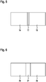
- the thermoelectric elements (1) each consist of small cuboids (2a, 2b) of p- and n-doped semiconductor material, which are alternately provided at the top and bottom with metal bridges (3a, 3b).
- the metal bridges (3a, 3b) form the thermal and electrical contacts of the thermoelectric elements (1) on a hot or a cold side (4, 5) of the thermoelectric module and are usually between two spaced ceramic plates (6a, 6b) arranged.
- the differently doped cuboids (2a, 2b) are interconnected by the metal bridges (3a, 3b) such that they result in a series connection.
- the connection points of the cuboids (2a, 2b) cool off on one side (4, 5), depending on the current intensity and the current direction, while on the opposite side (FIG. 4, 5).
- the applied current thus generates a temperature difference between the ceramic plates (6a, 6b). If, however, a different temperature at the opposite ceramic plates (6a, 6b), depending on the temperature difference, a current flow in the cuboids (2a, 2b) of each thermoelectric element (1) of the module is produced.
- the edge length (7) of the cuboids (2a, 2b) perpendicular to the ceramic plates (6a, 6b) is about 3 - 5 mm.
- the large edge length (7) causes a high thermal resistance between the hot and cold side (4, 5), so that the Seebeck voltage and the power of the module compared to a in Figure 2 shown Peltier module with shorter edge length (7) of the cuboid (2a, 2b), but the same cross-section of the cuboid (2a, 2b) is larger.
- the cuboids (2a, 2b) with a larger edge length (7) require more semiconductor material.
- thermoelectric materials The conversion efficiency of the conventional thermoelectric materials mentioned above is currently in the range below 5%. This means that the heat flow must be more than 20 times the required electrical power. Since the specific thermal conductivity of the usual, above-mentioned thermoelectric materials in the range of 1-5 W / mK, the specific thermal conductivity of the thermal contacts of the cuboid must be well above 20 - 100 W / mK.
- thermoelectric elements as in FIG. 2 shown, even more difficult to provide heat.
- thermoelectric device The US2006 / 0076046 discloses a thermoelectric device.
- thermoelectric element manufacturable by way of manufacturing methods for semiconductors having a first and a second thermoelectric leg, wherein the first leg on a first electrode and the second leg are arranged on a second electrode.
- a common electrode is also arranged on the first and second legs.
- the legs each consist of two semiconductor sections, which are each separated by a barrier section.
- the barrier section has a lower thermal but higher electrical conductivity than the adjacent semiconductor sections.
- the barrier section is intended to reduce the thermal conductivity of the leg and to improve its electrical conductivity.
- An insulating layer in which the legs are embedded extends over the full width of the thermoelectric element.
- thermoelectric element with high thermal resistance, which requires compared to a conventional thermoelectric element with comparable performance less semiconductor material. Furthermore, a method for producing such a thermoelectric element is to be specified.
- the object is interrupted by a thermoelectric element comprising a substrate having a substrate front side and a substrate rear side opposite the substrate front side, a first contact being applied as a layer on the substrate front side, a second contact being applied as a layer on the substrate front side between the first and second contacts, which thermally and electrically separate the first and second contacts from each other, wherein at least the course of the interruption between the first and second contact is not rectilinear and a thermoelectrically active layer having a top and a bottom, which are interconnected by lateral boundary surfaces, wherein the thermoelectrically active layer is arranged in the interruption such that the underside rests on the substrate front side and one of the lateral boundary surfaces on the first contact and one of the lateral boundary surfaces on the second contact abut.
- thermoelectric element according to the invention is that, taking into account the technical limits of the distance between the first and second contact and thus the thermal resistance is arbitrary, although the thermoelectrically active material is designed as a layer, in particular thin film. Despite the high thermal resistance of the space requirement of the thermoelectric element is extremely low, since both the electrical and thermal contacts and the thermoelectric material are applied as layers in a plane on the substrate surface. Furthermore, for the arranged in the interruption thermoelectric effect layer, despite the conventional thermoelectric elements after illustration 1 comparable thermal resistance, significantly less thermoelectric material needed.
- thermoelectrically active layer Assuming a constant layer thickness, the lateral boundary surfaces of the thermoelectrically active layer, which bear against the first and second contacts, increase in comparison to a straight-line course. As a result, the electrical resistance between the contacts and the thermoelectric active layer is reduced. The thermal resistance, however, remains opposite to a straight-line course of the interruption assuming the matching width of the interruption sufficiently high. This results in a further improved performance of the thermoelectric element.
- the disadvantages of the prior art are eliminated, according to which the coupling and decoupling takes place via the cross section of the cuboid, which always remains constant regardless of its edge length.
- the size of the abutment surface between the lateral boundary surfaces and the first and second contact can be varied within wide limits.
- the interruption is carried out in particular as a trench between the contacts.
- the trench on both sides limiting lateral edges of the contacts are preferably inclined relative to the substrate front side.
- the inclined edges in the direction of the trench interior promote the deposition of the thermoelectrically active layer in the interruption.
- the via between the front and back of the substrate between the first and third and the second and fourth contacts may be performed, for example, as an internally metallized bore through the substrate.
- all layers on the substrate front side and on the substrate rear side are preferably applied as thin layers.
- the thickness of the layers deposited by way of thin-film technology is typically in the range of a few micrometers; it is at most 100 microns.
- thermoelectrically active layer has a plurality of layers of an adhesive material and a plurality of layers of a thermoelectric material and the layers of adhesive material and thermoelectric material alternate between the top and bottom of the thermoelectric layer, this causes the thermoelectric layer to be mechanically more stable as a layer exclusively of thermoelectric material and at the same time has a lower thermal expansion coefficient. In this way, a detachment of the lateral boundary surfaces of the thermoelectrically active layer from the first or second contact is prevented in particular.
- An ancestor for making a thermoelectric element comprises the steps of depositing a metallization layer on a substrate front side of a substrate, patterning an interruption in the metallization layer by selectively removing the metallization layer from the substrate front side so that the interruption divides the metallization into a first contact and a second contact Depositing a thermoelectrically active layer into the interruption so that the interruption is at least partially filled with the layer of thermoelectrically active material.
- the substrate used is, for example, a plate or foil, in particular of polyimide.
- the plate may in particular be glass fiber reinforced.
- copper or another thermally and electrically highly conductive metal is applied as the metallization layer.
- thermoelectrically active layer at least thermoelectric material, in particular bismuth telluride or another of the conventional semiconductor materials mentioned at the outset, is deposited in the previously structured interruption.
- the manufacturing method additionally comprises the steps of applying a metallization layer on a rear side of the substrate opposite the substrate front side, structuring an interruption in the metallization layer on the rear side by targeted removal of the metallization layer from the substrate rear side the interruption divides the metallization into a third contact and a fourth contact, producing at least one first via that thermally and electrically interconnects and fabricates the first and third contacts at least one second via, which thermally and electrically interconnects the second and fourth contacts.
- the metallization of the rear side copper or another thermally and electrically highly conductive metal is likewise preferably used.
- To produce the via holes may be introduced into the substrate, which in turn are metallized in order to electrically and thermally conductively connect the metallization layers applied to the front and rear sides.
- the deposition of the layers as thin layers is preferably carried out by methods of physical or chemical vapor deposition.
- methods of physical or chemical vapor deposition As a preferred method of physical vapor deposition, in particular sputtering comes into consideration.
- the structuring of the metallization layers preferably takes place within the framework of the etching customary in semiconductor technology.
- dry etching processes such as plasma etching, reactive ion deep etching and wet-chemical processes are possible.
- thermoelectrically active layer in the interruption, an adhesive material is first deposited on the substrate surface. Titanium (Ti) is particularly suitable as adhesive material. Then alternating layers of thermoelectric material, such as bismuth telluride, and adhesive material, such as titanium, deposited.
- FIG. 3 shows a first embodiment of a thermoelectric element (10) with a planar substrate (11) made of polyimide with a substrate front side (12) and one of the substrate front side (12) opposite the substrate rear side (13).
- a first contact (14) and a second contact (15) applied as a copper layer.
- the layers are not to scale the invention to scale, but shown exaggerated.
- the actual thickness of the copper layer is a maximum of 100 ⁇ m.
- the layers forming the two contacts (14, 15) are rectangular. Between the first contact (14) and the second contact (15) there is an interruption (16) which thermally and electrically separates the first contact (14) and the second contact (15) from each other.
- the interruption is in the supervision (cf. FIG.
- thermoelectrically active layer (17) running as a rectilinear rectangular trench between the two contacts (14, 15) extending over the entire length of the substrate (11) in the direction of the trench.
- a thermoelectrically active layer (17) is arranged in the interruption (16).
- the thermoelectrically active layer (17) is bounded by a top (18), a bottom (19) and the top and bottom (18, 19) interconnecting lateral boundary surfaces (20, 21), as can be seen from the enlarged view in FIG Figure 8 results.
- thermoelectrically active layer (17) is arranged in the interruption (16) such that the underside (19) rests on the substrate front side (12) and one of the lateral boundary surfaces (20) on the first contact (14) and one of the lateral boundary surfaces (21) abut the second contact (15).
- the heat flow (24) is coupled into or out of the thermoelectrically active layer (17) via the lateral boundary surfaces (20, 21).
- the connection of the thermoelectric element (10) to a heat source (22) takes place with the aid of the first contact (14) and the coupling of the thermoelectric element (10) to a heat sink (23) takes place with the aid of the second contact (15).
- the contact surfaces on the first and second contacts for the lateral boundary surfaces (20, 21) extend in the Practice preferably inclined to improve the deposition of the thermoelectric layer (17) by means of a physical vapor deposition process.
- thermoelectric element (10) in addition to the embodiment according to Figure 3 a third contact (25) and a fourth contact (26), which are each designed as a copper layer on the substrate rear side (13).
- a third contact (25) and a fourth contact (26) which are each designed as a copper layer on the substrate rear side (13).
- the interruption (27) runs in a straight line and extends in the running direction over the entire length of the substrate (11), as shown in the rear view of the thermoelectric element (10) in FIG Figure 6 is recognizable.
- a via (28) thermally and electrically connects the first contact (14) to the third contact (25) and a via (29) thermally and electrically connects the second contact (15) to the fourth contact (26).
- the vias (28, 29) are designed as a bore through the substrate (11), the borehole walls are metallized with copper.
- the additional contacts (25, 26) make it possible to couple in or out the heat via the rear side, wherein the heat flow (24) from the heat source (22) via the third contact (25), the via (28), the first Contact (14), the thermoelectric effect layer (17), the second contact (15), the via (29) and the fourth contact (26) flows.
- FIG. 7 shows a third embodiment of a thermoelectric element (10) in a perspective view, which in the construction of the substantially thermoelectric element with double-sided metallization of the substrate after Figure 4 equivalent.
- the Prevention of repetition of the comments on the structure of the thermoelectric element according to Figure 4 directed.
- a significant difference, however, is that the course of the interruption (16) between the first contact (14) and the second contact (15) is not straight, but according to the invention meandering.
- With matching dimensions of the substrate (11) of the thermoelectric elements (1C) according to Figures 4 and 7 can be increased by the meandering formation of the interruption (16) whose length.
- thermoelectric element (10) With the same dimensions of the thermoelectric element (10), the lateral boundary surfaces (20, 21) of the thermoelectrically active layer (17) which abut the first contact (14) and the second contact (15) increase.
- a substantially identical thermal resistance between the first and second contact (14, 15) of the thermoelectric element (10) with a matching thickness of the thermoelectrically active layer (17) a larger cross section of the contact surface is created so that the electrical resistance of the thermoelectric element decreases. Due to the non-linear course of the interruption therefore an important requirement for thermoelectric elements, namely a high electrical conductivity at the same time low thermal conductivity, met.
- thermoelectrically active layer The non-rectilinear, in particular meandering, course of the interruption allows, with the same electrical conductivity as a straight-line interruption, lower layer thicknesses of the thermoelectrically active layer. This results in advantages in the production of the thermoelectrically active layer by way of physical vapor deposition processes, since these become more expensive and expensive with increasing layer thickness.
- thermoelectrically active layer (17) comprises alternately layers (30) of an adhesive material, in particular titanium, and layers (31) of a thermoelectric material, in particular bismuth telluride. Through this multilayered. Construction results in a mechanically more stable layer with a lower coefficient of thermal expansion than pure thermoe-ektharide. This prevents detachment of the thermoelectrically effective layer (17) at the lateral boundary surfaces (20, 21) from the first and second contacts (14, 15).
- the substrate (11) made of glass fiber reinforced polyimide is first laminated with copper on one or both sides.
- the interruption (16) and possibly the further interruption (27) is structured by etching.
- the thermoelectrically active layer (17) is then introduced by means of a sputtering process. If the thermoelectrically active layer (17) is multilayered, first the layer of adhesive material (30) is deposited on the substrate front side (12) and then alternating layers of thermoelectric material (31) and layers of adhesive material (30). If the thermoelectric element (10) according to Figures 4-7 has contacts on both sides, in addition, the plated-through holes (28, 29) by drilling the substrate (11) and then metallizing the holes must be made.
- thermoelectric elements (10) are all characterized in that the heat flow (24) in a common, through the contacts on the front and the thermoelectrically active layer spanned plane flows. As a result, the thermoelectric element (10) builds compact and requires only a small amount of thermoelectric material at high thermal resistance. In addition, the electrical resistance of the thermoelectric element can be lowered by adjusting the course of the interruption. ⁇ B> LIST OF REFERENCES ⁇ / b> No. description No.
- thermoelectric element 29 via 2 a, b cuboid 30 Location of adhesive material 3 a, b metal bridges 31 Location thermoelectric material 4 hot side 32 5 cold side 33 6 a, b ceramic plates 34 7 box length 35 8th - 36 9 - 37 10 thermoelectric element 38 11 substratum 39 12 Substrate front 40 13 Substrate back 41 14 first contact 42 15 second contact 43 16 interruption 44 17 thermoelectrically active layer 45 18 top 46 19 bottom 47 20 lateral boundary surface 48 21 lateral boundary surface 49 22 heat source 50 23 heat sink 51 24 heat flow 52 25 third contact 53 26 fourth contact 54 27 interruption 55 28 via 56
Landscapes
- Engineering & Computer Science (AREA)
- Manufacturing & Machinery (AREA)
- Chemical & Material Sciences (AREA)
- Inorganic Chemistry (AREA)
- Cooling Or The Like Of Semiconductors Or Solid State Devices (AREA)
- Measuring Temperature Or Quantity Of Heat (AREA)
Claims (10)
- Élément thermoélectrique (10), comprenant- un substrat (11) avec une face avant (12) de substrat et une face arrière (13) de substrat opposée à la face avant (12) de substrat,- un premier contact (14) qui est appliqué en tant que couche sur la face avant (12) de substrat,- un deuxième contact (15) qui est appliqué en tant que couche sur la face avant (12) de substrat,- une interruption (16) entre le premier et le deuxième contacts (14, 15), qui sépare thermiquement et électriquement l'un de l'autre le premier et le deuxième contacts,- au moins le tracé de l'interruption (16) entre le premier et le deuxième contacts (14, 15) n'étant pas rectiligne et- une couche (17) thermo-électriquement active, avec une face supérieure (18) et une face inférieure (19) qui sont reliées l'une à l'autre par des surfaces de délimitation (20, 21) latérales,- la couche (17) thermo-électriquement active étant placée dans l'interruption (16) de telle sorte que la face inférieure (19) s'appuie sur la face avant (12) de substrat et que l'une des surfaces de délimitation (20) latérales s'appuie sur le premier contact (14) et que l'une (21) des surfaces de délimitation latérales s'appuie sur le deuxième contact (15).
- Élément thermoélectrique selon la revendication 1, caractérisé- en ce qu'un troisième contact (25) est appliqué en tant que couche sur la face arrière (13) de substrat,- en ce qu'un quatrième contact (26) est appliqué en tant que couche sur la face arrière (13) de substrat,- en ce qu'une interruption (27) est placée entre le troisième et le quatrième contacts (25, 26), qui sépare thermiquement et électriquement l'un de l'autre le troisième et le quatrième contacts,- en ce qu'au moins un premier via (28) relie thermiquement et électriquement l'un à l'autre le premier et le troisième contacts (14, 25) et- en ce qu'au moins un deuxième via (29) relie thermiquement et électriquement l'un à l'autre le deuxième et le quatrième contact (15, 26).
- Élément thermoélectrique selon la revendication 1 ou la revendication 2, caractérisé en ce que toutes les couches sur la face avant (12) de substrat et sur la face arrière (13) de substrat sont appliquées en couches minces.
- Élément thermoélectrique selon l'une quelconque des revendications 1 à 3, caractérisé en ce que la couche (17) thermo-électriquement active comporte plusieurs couches en une matière adhésive (30) et plusieurs couches en une matière thermoélectrique (31) et en ce que les couches (30, 31) en matière adhésive et en matière thermoélectrique s'alternent entre les faces supérieure et inférieure (18, 19) de la couche (17) thermo-électriquement active.
- Élément thermoélectrique selon l'une quelconque des revendications 1 à 4, caractérisé en ce que l'épaisseur de la couche (17) thermo-électriquement active est supérieure à l'épaisseur du premier et du deuxième contacts (14, 15) et en ce que la couche (17) thermo-électriquement active chevauche partiellement le premier et le deuxième contacts (14, 15).
- Procédé destiné à fabriquer un élément thermoélectrique, comprenant les étapes- de l'application d'une couche de métallisation sur une face avant (12) de substrat d'un substrat (11),- de la structuration d'une interruption (16) dans la couche de métallisation par retrait ciblé de la couche de métallisation de la face avant (12) de substrat, de telle sorte que l'interruption (16) divise la métallisation en un premier contact (14) et un deuxième contact (15),- du dépôt d'une couche (17) thermo-électriquement active dans l'interruption (16), de sorte que l'interruption (16) se remplisse au moins partiellement de matière thermo-électriquement active ;au moins le tracé de l'interruption (16) entre le premier et le deuxième contacts (14, 15) n'étant pas rectiligne.
- Procédé selon la revendication 6, comprenant par ailleurs les étapes- de l'application d'une couche de métallisation sur une face arrière (13) de substrat qui est opposée à la face avant (12) de substrat,- de la structuration d'une interruption (27) dans la couche de métallisation sur la face arrière, par retrait ciblé de la couche de métallisation de la face arrière (13) de substrat, de sorte que l'interruption divise la métallisation en un troisième contact (25) et en un quatrième contact (26),- de la création d'au moins un premier via (28) qui relie l'un à l'autre thermiquement et électriquement le premier et le troisième contacts (14, 25),- de la création d'au moins un deuxième via (29) qui relie l'un à l'autre thermiquement et électriquement le deuxième et le quatrième contacts (15, 26).
- Procédé selon la revendication 6 ou la revendication 7, caractérisé en ce qu'on applique toutes les couches en tant que couches minces avec des procédés du dépôt physique ou chimique en phase vapeur.
- Procédé selon l'une quelconque des revendications 6 à 8, caractérisé en ce que la structuration de chaque couche de métallisation s'effectue par gravure.
- Procédé selon l'une quelconque des revendications 6 à 9, caractérisé en ce qu'on dépose la couche (17) thermo-électriquement active en plusieurs couches (30, 31) dans l'interruption (16), sachant que l'on dépose d'abord une couche de matière adhésive (30) sur la face avant (12) de substrat et ensuite en alternance des couches en matière thermo-électrique et en matière adhésive (30, 31).
Applications Claiming Priority (3)
| Application Number | Priority Date | Filing Date | Title |
|---|---|---|---|
| DE102012101492 | 2012-02-24 | ||
| DE102012105373.1A DE102012105373B4 (de) | 2012-02-24 | 2012-06-20 | Thermoelektrisches Element sowie Verfahren zu dessen Herstellung |
| PCT/EP2013/050802 WO2013124095A1 (fr) | 2012-02-24 | 2013-01-17 | Élément thermoelectrique |
Publications (2)
| Publication Number | Publication Date |
|---|---|
| EP2805360A1 EP2805360A1 (fr) | 2014-11-26 |
| EP2805360B1 true EP2805360B1 (fr) | 2017-06-14 |
Family
ID=48950712
Family Applications (1)
| Application Number | Title | Priority Date | Filing Date |
|---|---|---|---|
| EP13702941.9A Not-in-force EP2805360B1 (fr) | 2012-02-24 | 2013-01-17 | Élément thermoelectrique |
Country Status (7)
| Country | Link |
|---|---|
| US (1) | US9899588B2 (fr) |
| EP (1) | EP2805360B1 (fr) |
| JP (1) | JP2015511404A (fr) |
| CN (1) | CN104137283B (fr) |
| DE (2) | DE102012105373B4 (fr) |
| RU (1) | RU2606250C2 (fr) |
| WO (2) | WO2013124094A2 (fr) |
Families Citing this family (6)
| Publication number | Priority date | Publication date | Assignee | Title |
|---|---|---|---|---|
| US10267545B2 (en) | 2016-03-30 | 2019-04-23 | Qualcomm Incorporated | In-plane active cooling device for mobile electronics |
| US20170337269A1 (en) * | 2016-05-17 | 2017-11-23 | Charles Eugene Gafford, III | System for sharing musical preferences |
| DE102017203643A1 (de) | 2017-03-07 | 2018-09-13 | Mahle International Gmbh | Verfahren zum Herstellen von thermoelektrischen Bausteinen |
| DE102017115168B4 (de) * | 2017-07-06 | 2019-02-14 | Mahle International Gmbh | Thermoelektrisches Modul |
| DE102017217123A1 (de) * | 2017-09-26 | 2019-03-28 | Mahle International Gmbh | Verfahren zum Herstellen eines thermoelektrischen Wandlers |
| DE102021209656B3 (de) * | 2021-09-02 | 2022-09-29 | Nikolay Iosad | Thermoelektrisches Element, thermoelektrischer Generator und Verfahren zu deren Herstellung |
Citations (1)
| Publication number | Priority date | Publication date | Assignee | Title |
|---|---|---|---|---|
| US20060076046A1 (en) * | 2004-10-08 | 2006-04-13 | Nanocoolers, Inc. | Thermoelectric device structure and apparatus incorporating same |
Family Cites Families (30)
| Publication number | Priority date | Publication date | Assignee | Title |
|---|---|---|---|---|
| CH413018A (de) * | 1963-04-30 | 1966-05-15 | Du Pont | Thermoelektrischer Generator |
| US4538464A (en) * | 1983-10-04 | 1985-09-03 | The United States Of America As Represented By The United States Department Of Energy | Method of measuring reactive acoustic power density in a fluid |
| RU2113035C1 (ru) * | 1988-02-22 | 1998-06-10 | Миговски Фридрих-Карл | Термогенератор |
| JPH0769221B2 (ja) * | 1991-10-09 | 1995-07-26 | 工業技術院長 | 温度検知材料、温度センサー及び温度測定方法 |
| US5554819A (en) * | 1992-01-22 | 1996-09-10 | Baghai-Kermani; A. | Method and apparatus for the thermoelectric generation of electricity |
| JPH0629581A (ja) * | 1992-07-09 | 1994-02-04 | Matsushita Electric Ind Co Ltd | 熱電素子 |
| JPH06188464A (ja) * | 1992-12-17 | 1994-07-08 | Matsushita Electric Ind Co Ltd | 薄膜熱電素子及びその製造方法 |
| JPH10173110A (ja) * | 1996-12-13 | 1998-06-26 | Nissan Motor Co Ltd | 電子冷却モジュールおよびその製造方法 |
| US6046398A (en) * | 1998-11-04 | 2000-04-04 | The United States Of America As Represented By The Administrator Of The National Aeronautics And Space Administration | Micromachined thermoelectric sensors and arrays and process for producing |
| US6281120B1 (en) * | 1998-12-18 | 2001-08-28 | National Semiconductor Corporation | Temperature control structure for integrated circuit |
| JP2001332773A (ja) * | 2000-05-19 | 2001-11-30 | Yamaha Corp | 熱電モジュール用多層基板およびその製造方法ならびにこの多層基板を用いた熱電モジュール |
| KR20040008155A (ko) * | 2001-04-09 | 2004-01-28 | 리써치 트라이앵글 인스티튜트 | Dna 게놈 및 프로테옴 칩용, 열광학 스위칭 회로용,그리고 ir 태그용 박막 열전기 냉각 및 가열 장치 |
| WO2003090286A1 (fr) * | 2002-04-15 | 2003-10-30 | Nextreme Thermal Solutions | Dispositif thermoelectrique utilisant des jonctions peltier double face et procede de fabrication de ce dispositif |
| US7122797B2 (en) * | 2002-09-09 | 2006-10-17 | Sensors Unlimited, Inc. | Method for making an infrared detector and infrared detector |
| JP3803365B2 (ja) * | 2003-11-17 | 2006-08-02 | 松下電器産業株式会社 | 結晶膜の製造方法、結晶膜付き基体の製造方法、および熱電変換素子の製造方法 |
| DE102004030043B4 (de) * | 2004-06-22 | 2006-05-04 | Infineon Technologies Ag | Verfahren zum Herstellen eines Thermoelements |
| WO2007002342A2 (fr) * | 2005-06-22 | 2007-01-04 | Nextreme Thermal Solutions | Procédés de fabrication de dispositifs thermoélectriques comprenant des matrices électriquement isolantes entre les traces conductrices et structures associées |
| DE202006002674U1 (de) * | 2006-02-20 | 2006-04-20 | Isabellenhütte Heusler Gmbh & Co. Kg | Füllstandssensor |
| US7626114B2 (en) * | 2006-06-16 | 2009-12-01 | Digital Angel Corporation | Thermoelectric power supply |
| EP1885004B1 (fr) * | 2006-07-24 | 2010-05-19 | C.R.F. Società Consortile per Azioni | Dispositif pour la conversion de radiation électromagnétique en énergie électrique et procédé de conversion correspondant |
| TWI338390B (en) * | 2007-07-12 | 2011-03-01 | Ind Tech Res Inst | Flexible thermoelectric device and manufacturing method thereof |
| WO2009063911A1 (fr) * | 2007-11-14 | 2009-05-22 | Murata Manufacturing Co., Ltd. | Partie de module de conversion thermoélectrique, module de conversion thermoélectrique, et procédé de fabrication de celui-ci |
| JP5298532B2 (ja) | 2007-12-27 | 2013-09-25 | ダイキン工業株式会社 | 熱電素子 |
| KR101063938B1 (ko) * | 2008-11-13 | 2011-09-14 | 한국전기연구원 | 중저온용 열전재료 |
| TWI405361B (zh) * | 2008-12-31 | 2013-08-11 | 財團法人工業技術研究院 | 熱電元件及其製程、晶片堆疊結構及晶片封裝結構 |
| JP5066564B2 (ja) * | 2009-07-06 | 2012-11-07 | 韓國電子通信研究院 | 熱電素子及びその製造方法 |
| US20110094556A1 (en) * | 2009-10-25 | 2011-04-28 | Digital Angel Corporation | Planar thermoelectric generator |
| JP5703585B2 (ja) * | 2010-04-13 | 2015-04-22 | 富士通株式会社 | 熱電変換素子及びその製造方法 |
| KR101097679B1 (ko) * | 2010-05-25 | 2011-12-23 | 삼성전기주식회사 | 에너지 변환 소자 및 그 제조 방법, 그리고 상기 에너지 변환 소자를 구비하는 전자 장치 |
| DE102010022668B4 (de) * | 2010-06-04 | 2012-02-02 | O-Flexx Technologies Gmbh | Thermoelektrisches Element und Modul umfassend mehrere derartige Elemente |
-
2012
- 2012-06-20 DE DE102012105373.1A patent/DE102012105373B4/de not_active Expired - Fee Related
- 2012-06-20 DE DE102012105367A patent/DE102012105367A1/de not_active Withdrawn
-
2013
- 2013-01-16 WO PCT/EP2013/050702 patent/WO2013124094A2/fr not_active Ceased
- 2013-01-17 RU RU2014138379A patent/RU2606250C2/ru not_active IP Right Cessation
- 2013-01-17 US US14/380,272 patent/US9899588B2/en active Active
- 2013-01-17 JP JP2014558042A patent/JP2015511404A/ja active Pending
- 2013-01-17 EP EP13702941.9A patent/EP2805360B1/fr not_active Not-in-force
- 2013-01-17 WO PCT/EP2013/050802 patent/WO2013124095A1/fr not_active Ceased
- 2013-01-17 CN CN201380010723.3A patent/CN104137283B/zh not_active Expired - Fee Related
Patent Citations (1)
| Publication number | Priority date | Publication date | Assignee | Title |
|---|---|---|---|---|
| US20060076046A1 (en) * | 2004-10-08 | 2006-04-13 | Nanocoolers, Inc. | Thermoelectric device structure and apparatus incorporating same |
Also Published As
| Publication number | Publication date |
|---|---|
| WO2013124095A1 (fr) | 2013-08-29 |
| JP2015511404A (ja) | 2015-04-16 |
| CN104137283B (zh) | 2018-03-23 |
| US20150034140A1 (en) | 2015-02-05 |
| EP2805360A1 (fr) | 2014-11-26 |
| RU2014138379A (ru) | 2016-04-10 |
| US9899588B2 (en) | 2018-02-20 |
| WO2013124094A2 (fr) | 2013-08-29 |
| WO2013124094A3 (fr) | 2013-10-24 |
| DE102012105367A1 (de) | 2013-08-29 |
| CN104137283A (zh) | 2014-11-05 |
| DE102012105373A1 (de) | 2013-08-29 |
| DE102012105373B4 (de) | 2019-02-07 |
| RU2606250C2 (ru) | 2017-01-10 |
Similar Documents
| Publication | Publication Date | Title |
|---|---|---|
| EP2805360B1 (fr) | Élément thermoelectrique | |
| DE69730822T2 (de) | Verfahren zur herstellung eines thermionischen elements | |
| DE69535235T2 (de) | Thermoelektrische Vorrichtung | |
| DE69321864T2 (de) | Verfahren und Vorrichtung zur Verkapselung von dreidimensionalen Halbleiterplättchen | |
| DE102012217807B4 (de) | Thermoelektrische Vorrichtungen und Verfahren zum Herstellen derselben | |
| DE102010022668B4 (de) | Thermoelektrisches Element und Modul umfassend mehrere derartige Elemente | |
| DE102008026801B4 (de) | Wärmeübertragungsvorrichtung zur doppelseitigen Kühlung eines Halbleiterbauelementes und Verfahren zu seiner Montage | |
| DE1180015C2 (de) | Mittel zur elektrischen Isolierung und ther-mischen Kontaktierung bei einer nach dem Seebeck- oder Peltier-Effekt arbeitenden thermoelektrischen Batterie | |
| DE102017125647B4 (de) | Thermoelektrische Vorrichtungen und Verfahren zum Bilden von thermoelektrischen Vorrichtungen | |
| DE102010029526A1 (de) | Halbleiterbauelement mit einer gestapelten Chipkonfiguration mit einem integrierten Peltier-Element | |
| WO2016198634A1 (fr) | Dispositif comprenant une feuille pour le couplage électrostatique d'un substrat avec un support de substrat | |
| DE10004390C2 (de) | Thermoelektrischer Generator und Verfahren zu seiner Herstellung | |
| EP2771917B1 (fr) | Thermoélément, son procédé de production et substrat servant à la mise en oeuvre de ce procédé | |
| DE10231445A1 (de) | Thermoelektrisches Element und Verfahren zum Herstellen eines thermoelektrischen Elements | |
| DE102020116671A1 (de) | Waferbonding | |
| EP2301088B1 (fr) | Module doté de plusieurs éléments thermoélectriques | |
| EP1642335B1 (fr) | Ensemble circuit integre a refroidissement et procede de fabrication dudit ensemble | |
| EP2245677B1 (fr) | Dispositif de transfert thermique pour un élément à couche mince thermoélectrique | |
| EP1520299B1 (fr) | Ensemble d'agencements de condensateurs integres, en particulier de condensateurs de grille integres | |
| EP2917944B1 (fr) | Élément thermoélectrique et procédé de fabrication correspondant | |
| EP2939279A1 (fr) | Convertisseur thermoélectrique | |
| DE102013204813A1 (de) | Verfahren und Vorprodukt zur Herstellung eines thermoelektrischen Moduls | |
| DE102006031164B4 (de) | Thermoelektrisches Dünnschichtelement sowie Verfahren zu dessen Herstellung | |
| DE112020002813T5 (de) | Isolierte Laserkühler | |
| DE102017115168B4 (de) | Thermoelektrisches Modul |
Legal Events
| Date | Code | Title | Description |
|---|---|---|---|
| PUAI | Public reference made under article 153(3) epc to a published international application that has entered the european phase |
Free format text: ORIGINAL CODE: 0009012 |
|
| 17P | Request for examination filed |
Effective date: 20140721 |
|
| AK | Designated contracting states |
Kind code of ref document: A1 Designated state(s): AL AT BE BG CH CY CZ DE DK EE ES FI FR GB GR HR HU IE IS IT LI LT LU LV MC MK MT NL NO PL PT RO RS SE SI SK SM TR |
|
| RIN1 | Information on inventor provided before grant (corrected) |
Inventor name: IOSAD, NIKOLAY Inventor name: SPAN, GERHARD Inventor name: SIEGLOCH, ARWED Inventor name: HAFERKAMP, JUERGEN |
|
| DAX | Request for extension of the european patent (deleted) | ||
| RAP1 | Party data changed (applicant data changed or rights of an application transferred) |
Owner name: O-FLEXX TECHNOLOGIES GMBH |
|
| GRAP | Despatch of communication of intention to grant a patent |
Free format text: ORIGINAL CODE: EPIDOSNIGR1 |
|
| INTG | Intention to grant announced |
Effective date: 20170307 |
|
| GRAS | Grant fee paid |
Free format text: ORIGINAL CODE: EPIDOSNIGR3 |
|
| GRAA | (expected) grant |
Free format text: ORIGINAL CODE: 0009210 |
|
| AK | Designated contracting states |
Kind code of ref document: B1 Designated state(s): AL AT BE BG CH CY CZ DE DK EE ES FI FR GB GR HR HU IE IS IT LI LT LU LV MC MK MT NL NO PL PT RO RS SE SI SK SM TR |
|
| REG | Reference to a national code |
Ref country code: GB Ref legal event code: FG4D Free format text: NOT ENGLISH |
|
| REG | Reference to a national code |
Ref country code: CH Ref legal event code: EP Ref country code: AT Ref legal event code: REF Ref document number: 901723 Country of ref document: AT Kind code of ref document: T Effective date: 20170615 |
|
| REG | Reference to a national code |
Ref country code: IE Ref legal event code: FG4D Free format text: LANGUAGE OF EP DOCUMENT: GERMAN |
|
| REG | Reference to a national code |
Ref country code: DE Ref legal event code: R096 Ref document number: 502013007489 Country of ref document: DE |
|
| REG | Reference to a national code |
Ref country code: NL Ref legal event code: MP Effective date: 20170614 |
|
| REG | Reference to a national code |
Ref country code: LT Ref legal event code: MG4D |
|
| PG25 | Lapsed in a contracting state [announced via postgrant information from national office to epo] |
Ref country code: NO Free format text: LAPSE BECAUSE OF FAILURE TO SUBMIT A TRANSLATION OF THE DESCRIPTION OR TO PAY THE FEE WITHIN THE PRESCRIBED TIME-LIMIT Effective date: 20170914 Ref country code: LT Free format text: LAPSE BECAUSE OF FAILURE TO SUBMIT A TRANSLATION OF THE DESCRIPTION OR TO PAY THE FEE WITHIN THE PRESCRIBED TIME-LIMIT Effective date: 20170614 Ref country code: FI Free format text: LAPSE BECAUSE OF FAILURE TO SUBMIT A TRANSLATION OF THE DESCRIPTION OR TO PAY THE FEE WITHIN THE PRESCRIBED TIME-LIMIT Effective date: 20170614 Ref country code: GR Free format text: LAPSE BECAUSE OF FAILURE TO SUBMIT A TRANSLATION OF THE DESCRIPTION OR TO PAY THE FEE WITHIN THE PRESCRIBED TIME-LIMIT Effective date: 20170915 Ref country code: HR Free format text: LAPSE BECAUSE OF FAILURE TO SUBMIT A TRANSLATION OF THE DESCRIPTION OR TO PAY THE FEE WITHIN THE PRESCRIBED TIME-LIMIT Effective date: 20170614 |
|
| PG25 | Lapsed in a contracting state [announced via postgrant information from national office to epo] |
Ref country code: RS Free format text: LAPSE BECAUSE OF FAILURE TO SUBMIT A TRANSLATION OF THE DESCRIPTION OR TO PAY THE FEE WITHIN THE PRESCRIBED TIME-LIMIT Effective date: 20170614 Ref country code: BG Free format text: LAPSE BECAUSE OF FAILURE TO SUBMIT A TRANSLATION OF THE DESCRIPTION OR TO PAY THE FEE WITHIN THE PRESCRIBED TIME-LIMIT Effective date: 20170914 Ref country code: LV Free format text: LAPSE BECAUSE OF FAILURE TO SUBMIT A TRANSLATION OF THE DESCRIPTION OR TO PAY THE FEE WITHIN THE PRESCRIBED TIME-LIMIT Effective date: 20170614 Ref country code: SE Free format text: LAPSE BECAUSE OF FAILURE TO SUBMIT A TRANSLATION OF THE DESCRIPTION OR TO PAY THE FEE WITHIN THE PRESCRIBED TIME-LIMIT Effective date: 20170614 Ref country code: NL Free format text: LAPSE BECAUSE OF FAILURE TO SUBMIT A TRANSLATION OF THE DESCRIPTION OR TO PAY THE FEE WITHIN THE PRESCRIBED TIME-LIMIT Effective date: 20170614 |
|
| REG | Reference to a national code |
Ref country code: FR Ref legal event code: PLFP Year of fee payment: 6 |
|
| REG | Reference to a national code |
Ref country code: FR Ref legal event code: PLFP Year of fee payment: 6 |
|
| PG25 | Lapsed in a contracting state [announced via postgrant information from national office to epo] |
Ref country code: SK Free format text: LAPSE BECAUSE OF FAILURE TO SUBMIT A TRANSLATION OF THE DESCRIPTION OR TO PAY THE FEE WITHIN THE PRESCRIBED TIME-LIMIT Effective date: 20170614 Ref country code: CZ Free format text: LAPSE BECAUSE OF FAILURE TO SUBMIT A TRANSLATION OF THE DESCRIPTION OR TO PAY THE FEE WITHIN THE PRESCRIBED TIME-LIMIT Effective date: 20170614 Ref country code: EE Free format text: LAPSE BECAUSE OF FAILURE TO SUBMIT A TRANSLATION OF THE DESCRIPTION OR TO PAY THE FEE WITHIN THE PRESCRIBED TIME-LIMIT Effective date: 20170614 Ref country code: RO Free format text: LAPSE BECAUSE OF FAILURE TO SUBMIT A TRANSLATION OF THE DESCRIPTION OR TO PAY THE FEE WITHIN THE PRESCRIBED TIME-LIMIT Effective date: 20170614 |
|
| PG25 | Lapsed in a contracting state [announced via postgrant information from national office to epo] |
Ref country code: PL Free format text: LAPSE BECAUSE OF FAILURE TO SUBMIT A TRANSLATION OF THE DESCRIPTION OR TO PAY THE FEE WITHIN THE PRESCRIBED TIME-LIMIT Effective date: 20170614 Ref country code: IS Free format text: LAPSE BECAUSE OF FAILURE TO SUBMIT A TRANSLATION OF THE DESCRIPTION OR TO PAY THE FEE WITHIN THE PRESCRIBED TIME-LIMIT Effective date: 20171014 Ref country code: SM Free format text: LAPSE BECAUSE OF FAILURE TO SUBMIT A TRANSLATION OF THE DESCRIPTION OR TO PAY THE FEE WITHIN THE PRESCRIBED TIME-LIMIT Effective date: 20170614 Ref country code: ES Free format text: LAPSE BECAUSE OF FAILURE TO SUBMIT A TRANSLATION OF THE DESCRIPTION OR TO PAY THE FEE WITHIN THE PRESCRIBED TIME-LIMIT Effective date: 20170614 Ref country code: IT Free format text: LAPSE BECAUSE OF FAILURE TO SUBMIT A TRANSLATION OF THE DESCRIPTION OR TO PAY THE FEE WITHIN THE PRESCRIBED TIME-LIMIT Effective date: 20170614 |
|
| REG | Reference to a national code |
Ref country code: DE Ref legal event code: R082 Ref document number: 502013007489 Country of ref document: DE Representative=s name: BSB ANWALTSKANZLEI, DE Ref country code: DE Ref legal event code: R081 Ref document number: 502013007489 Country of ref document: DE Owner name: MAHLE INTERNATIONAL GMBH, DE Free format text: FORMER OWNER: O-FLEXX TECHNOLOGIES GMBH, 47059 DUISBURG, DE Ref country code: DE Ref legal event code: R082 Ref document number: 502013007489 Country of ref document: DE Representative=s name: BSB PATENTANWAELTE SCHUETTE & ENGELEN PARTNERS, DE Ref country code: DE Ref legal event code: R082 Ref document number: 502013007489 Country of ref document: DE Representative=s name: BRP RENAUD UND PARTNER MBB RECHTSANWAELTE PATE, DE |
|
| REG | Reference to a national code |
Ref country code: DE Ref legal event code: R097 Ref document number: 502013007489 Country of ref document: DE |
|
| PLBE | No opposition filed within time limit |
Free format text: ORIGINAL CODE: 0009261 |
|
| STAA | Information on the status of an ep patent application or granted ep patent |
Free format text: STATUS: NO OPPOSITION FILED WITHIN TIME LIMIT |
|
| PG25 | Lapsed in a contracting state [announced via postgrant information from national office to epo] |
Ref country code: DK Free format text: LAPSE BECAUSE OF FAILURE TO SUBMIT A TRANSLATION OF THE DESCRIPTION OR TO PAY THE FEE WITHIN THE PRESCRIBED TIME-LIMIT Effective date: 20170614 |
|
| PGFP | Annual fee paid to national office [announced via postgrant information from national office to epo] |
Ref country code: NO Payment date: 20180130 Year of fee payment: 6 |
|
| 26N | No opposition filed |
Effective date: 20180315 |
|
| REG | Reference to a national code |
Ref country code: DE Ref legal event code: R082 Ref document number: 502013007489 Country of ref document: DE Representative=s name: BRP RENAUD UND PARTNER MBB RECHTSANWAELTE PATE, DE |
|
| PGFP | Annual fee paid to national office [announced via postgrant information from national office to epo] |
Ref country code: FR Payment date: 20180129 Year of fee payment: 6 |
|
| R26N | No opposition filed (corrected) |
Effective date: 20180315 |
|
| PG25 | Lapsed in a contracting state [announced via postgrant information from national office to epo] |
Ref country code: SI Free format text: LAPSE BECAUSE OF FAILURE TO SUBMIT A TRANSLATION OF THE DESCRIPTION OR TO PAY THE FEE WITHIN THE PRESCRIBED TIME-LIMIT Effective date: 20170614 |
|
| REG | Reference to a national code |
Ref country code: CH Ref legal event code: PL |
|
| PG25 | Lapsed in a contracting state [announced via postgrant information from national office to epo] |
Ref country code: MT Free format text: LAPSE BECAUSE OF FAILURE TO SUBMIT A TRANSLATION OF THE DESCRIPTION OR TO PAY THE FEE WITHIN THE PRESCRIBED TIME-LIMIT Effective date: 20170614 |
|
| REG | Reference to a national code |
Ref country code: FR Ref legal event code: CD Owner name: MAHLE THERMOELEKTRONIK GMBH, DE Effective date: 20180925 |
|
| PG25 | Lapsed in a contracting state [announced via postgrant information from national office to epo] |
Ref country code: LU Free format text: LAPSE BECAUSE OF NON-PAYMENT OF DUE FEES Effective date: 20180117 |
|
| REG | Reference to a national code |
Ref country code: IE Ref legal event code: MM4A |
|
| REG | Reference to a national code |
Ref country code: BE Ref legal event code: MM Effective date: 20180131 |
|
| PG25 | Lapsed in a contracting state [announced via postgrant information from national office to epo] |
Ref country code: LI Free format text: LAPSE BECAUSE OF NON-PAYMENT OF DUE FEES Effective date: 20180131 Ref country code: BE Free format text: LAPSE BECAUSE OF NON-PAYMENT OF DUE FEES Effective date: 20180131 Ref country code: CH Free format text: LAPSE BECAUSE OF NON-PAYMENT OF DUE FEES Effective date: 20180131 |
|
| PG25 | Lapsed in a contracting state [announced via postgrant information from national office to epo] |
Ref country code: IE Free format text: LAPSE BECAUSE OF NON-PAYMENT OF DUE FEES Effective date: 20180117 |
|
| REG | Reference to a national code |
Ref country code: AT Ref legal event code: MM01 Ref document number: 901723 Country of ref document: AT Kind code of ref document: T Effective date: 20180117 |
|
| PG25 | Lapsed in a contracting state [announced via postgrant information from national office to epo] |
Ref country code: AT Free format text: LAPSE BECAUSE OF NON-PAYMENT OF DUE FEES Effective date: 20180117 |
|
| PG25 | Lapsed in a contracting state [announced via postgrant information from national office to epo] |
Ref country code: MC Free format text: LAPSE BECAUSE OF FAILURE TO SUBMIT A TRANSLATION OF THE DESCRIPTION OR TO PAY THE FEE WITHIN THE PRESCRIBED TIME-LIMIT Effective date: 20170614 |
|
| GBPC | Gb: european patent ceased through non-payment of renewal fee |
Effective date: 20190117 |
|
| PG25 | Lapsed in a contracting state [announced via postgrant information from national office to epo] |
Ref country code: FR Free format text: LAPSE BECAUSE OF NON-PAYMENT OF DUE FEES Effective date: 20190131 |
|
| PG25 | Lapsed in a contracting state [announced via postgrant information from national office to epo] |
Ref country code: GB Free format text: LAPSE BECAUSE OF NON-PAYMENT OF DUE FEES Effective date: 20190117 |
|
| PG25 | Lapsed in a contracting state [announced via postgrant information from national office to epo] |
Ref country code: TR Free format text: LAPSE BECAUSE OF FAILURE TO SUBMIT A TRANSLATION OF THE DESCRIPTION OR TO PAY THE FEE WITHIN THE PRESCRIBED TIME-LIMIT Effective date: 20170614 |
|
| PG25 | Lapsed in a contracting state [announced via postgrant information from national office to epo] |
Ref country code: HU Free format text: LAPSE BECAUSE OF FAILURE TO SUBMIT A TRANSLATION OF THE DESCRIPTION OR TO PAY THE FEE WITHIN THE PRESCRIBED TIME-LIMIT; INVALID AB INITIO Effective date: 20130117 Ref country code: PT Free format text: LAPSE BECAUSE OF FAILURE TO SUBMIT A TRANSLATION OF THE DESCRIPTION OR TO PAY THE FEE WITHIN THE PRESCRIBED TIME-LIMIT Effective date: 20170614 |
|
| PG25 | Lapsed in a contracting state [announced via postgrant information from national office to epo] |
Ref country code: MK Free format text: LAPSE BECAUSE OF NON-PAYMENT OF DUE FEES Effective date: 20170614 Ref country code: CY Free format text: LAPSE BECAUSE OF FAILURE TO SUBMIT A TRANSLATION OF THE DESCRIPTION OR TO PAY THE FEE WITHIN THE PRESCRIBED TIME-LIMIT Effective date: 20170614 |
|
| PG25 | Lapsed in a contracting state [announced via postgrant information from national office to epo] |
Ref country code: AL Free format text: LAPSE BECAUSE OF FAILURE TO SUBMIT A TRANSLATION OF THE DESCRIPTION OR TO PAY THE FEE WITHIN THE PRESCRIBED TIME-LIMIT Effective date: 20170614 |
|
| PGFP | Annual fee paid to national office [announced via postgrant information from national office to epo] |
Ref country code: DE Payment date: 20210329 Year of fee payment: 9 |
|
| REG | Reference to a national code |
Ref country code: DE Ref legal event code: R119 Ref document number: 502013007489 Country of ref document: DE |
|
| PG25 | Lapsed in a contracting state [announced via postgrant information from national office to epo] |
Ref country code: DE Free format text: LAPSE BECAUSE OF NON-PAYMENT OF DUE FEES Effective date: 20220802 |