EP2762272A2 - Wafer polishing apparatus and method - Google Patents
Wafer polishing apparatus and method Download PDFInfo
- Publication number
- EP2762272A2 EP2762272A2 EP14020009.8A EP14020009A EP2762272A2 EP 2762272 A2 EP2762272 A2 EP 2762272A2 EP 14020009 A EP14020009 A EP 14020009A EP 2762272 A2 EP2762272 A2 EP 2762272A2
- Authority
- EP
- European Patent Office
- Prior art keywords
- polishing
- edge portion
- polishing tool
- substrate
- wafer
- Prior art date
- Legal status (The legal status is an assumption and is not a legal conclusion. Google has not performed a legal analysis and makes no representation as to the accuracy of the status listed.)
- Granted
Links
- 238000005498 polishing Methods 0.000 title claims abstract description 249
- 238000000034 method Methods 0.000 title description 8
- 239000000758 substrate Substances 0.000 claims abstract description 64
- 238000003825 pressing Methods 0.000 claims abstract description 32
- 238000004519 manufacturing process Methods 0.000 claims description 9
- 239000004065 semiconductor Substances 0.000 claims 16
- 238000007517 polishing process Methods 0.000 abstract description 3
- 239000007788 liquid Substances 0.000 description 7
- XUIMIQQOPSSXEZ-UHFFFAOYSA-N Silicon Chemical compound [Si] XUIMIQQOPSSXEZ-UHFFFAOYSA-N 0.000 description 6
- 230000002093 peripheral effect Effects 0.000 description 6
- 229910052710 silicon Inorganic materials 0.000 description 6
- 239000010703 silicon Substances 0.000 description 6
- 238000010586 diagram Methods 0.000 description 4
- 239000012212 insulator Substances 0.000 description 3
- 239000006061 abrasive grain Substances 0.000 description 2
- XLYOFNOQVPJJNP-UHFFFAOYSA-N water Substances O XLYOFNOQVPJJNP-UHFFFAOYSA-N 0.000 description 2
- 238000012986 modification Methods 0.000 description 1
- 230000004048 modification Effects 0.000 description 1
Images


Classifications
-
- B—PERFORMING OPERATIONS; TRANSPORTING
- B24—GRINDING; POLISHING
- B24B—MACHINES, DEVICES, OR PROCESSES FOR GRINDING OR POLISHING; DRESSING OR CONDITIONING OF ABRADING SURFACES; FEEDING OF GRINDING, POLISHING, OR LAPPING AGENTS
- B24B21/00—Machines or devices using grinding or polishing belts; Accessories therefor
- B24B21/002—Machines or devices using grinding or polishing belts; Accessories therefor for grinding edges or bevels
-
- B—PERFORMING OPERATIONS; TRANSPORTING
- B24—GRINDING; POLISHING
- B24B—MACHINES, DEVICES, OR PROCESSES FOR GRINDING OR POLISHING; DRESSING OR CONDITIONING OF ABRADING SURFACES; FEEDING OF GRINDING, POLISHING, OR LAPPING AGENTS
- B24B9/00—Machines or devices designed for grinding edges or bevels on work or for removing burrs; Accessories therefor
- B24B9/02—Machines or devices designed for grinding edges or bevels on work or for removing burrs; Accessories therefor characterised by a special design with respect to properties of materials specific to articles to be ground
- B24B9/06—Machines or devices designed for grinding edges or bevels on work or for removing burrs; Accessories therefor characterised by a special design with respect to properties of materials specific to articles to be ground of non-metallic inorganic material, e.g. stone, ceramics, porcelain
- B24B9/065—Machines or devices designed for grinding edges or bevels on work or for removing burrs; Accessories therefor characterised by a special design with respect to properties of materials specific to articles to be ground of non-metallic inorganic material, e.g. stone, ceramics, porcelain of thin, brittle parts, e.g. semiconductors, wafers
-
- B—PERFORMING OPERATIONS; TRANSPORTING
- B24—GRINDING; POLISHING
- B24B—MACHINES, DEVICES, OR PROCESSES FOR GRINDING OR POLISHING; DRESSING OR CONDITIONING OF ABRADING SURFACES; FEEDING OF GRINDING, POLISHING, OR LAPPING AGENTS
- B24B21/00—Machines or devices using grinding or polishing belts; Accessories therefor
- B24B21/004—Machines or devices using grinding or polishing belts; Accessories therefor using abrasive rolled strips
-
- B—PERFORMING OPERATIONS; TRANSPORTING
- B24—GRINDING; POLISHING
- B24B—MACHINES, DEVICES, OR PROCESSES FOR GRINDING OR POLISHING; DRESSING OR CONDITIONING OF ABRADING SURFACES; FEEDING OF GRINDING, POLISHING, OR LAPPING AGENTS
- B24B21/00—Machines or devices using grinding or polishing belts; Accessories therefor
- B24B21/008—Machines comprising two or more tools or having several working posts
-
- B—PERFORMING OPERATIONS; TRANSPORTING
- B24—GRINDING; POLISHING
- B24B—MACHINES, DEVICES, OR PROCESSES FOR GRINDING OR POLISHING; DRESSING OR CONDITIONING OF ABRADING SURFACES; FEEDING OF GRINDING, POLISHING, OR LAPPING AGENTS
- B24B21/00—Machines or devices using grinding or polishing belts; Accessories therefor
- B24B21/04—Machines or devices using grinding or polishing belts; Accessories therefor for grinding plane surfaces
- B24B21/06—Machines or devices using grinding or polishing belts; Accessories therefor for grinding plane surfaces involving members with limited contact area pressing the belt against the work, e.g. shoes sweeping across the whole area to be ground
-
- B—PERFORMING OPERATIONS; TRANSPORTING
- B24—GRINDING; POLISHING
- B24B—MACHINES, DEVICES, OR PROCESSES FOR GRINDING OR POLISHING; DRESSING OR CONDITIONING OF ABRADING SURFACES; FEEDING OF GRINDING, POLISHING, OR LAPPING AGENTS
- B24B27/00—Other grinding machines or devices
- B24B27/0076—Other grinding machines or devices grinding machines comprising two or more grinding tools
-
- H—ELECTRICITY
- H01—ELECTRIC ELEMENTS
- H01L—SEMICONDUCTOR DEVICES NOT COVERED BY CLASS H10
- H01L21/00—Processes or apparatus adapted for the manufacture or treatment of semiconductor or solid state devices or of parts thereof
- H01L21/02—Manufacture or treatment of semiconductor devices or of parts thereof
- H01L21/02002—Preparing wafers
- H01L21/02005—Preparing bulk and homogeneous wafers
- H01L21/02035—Shaping
-
- H—ELECTRICITY
- H01—ELECTRIC ELEMENTS
- H01L—SEMICONDUCTOR DEVICES NOT COVERED BY CLASS H10
- H01L21/00—Processes or apparatus adapted for the manufacture or treatment of semiconductor or solid state devices or of parts thereof
- H01L21/02—Manufacture or treatment of semiconductor devices or of parts thereof
- H01L21/04—Manufacture or treatment of semiconductor devices or of parts thereof the devices having potential barriers, e.g. a PN junction, depletion layer or carrier concentration layer
- H01L21/34—Manufacture or treatment of semiconductor devices or of parts thereof the devices having potential barriers, e.g. a PN junction, depletion layer or carrier concentration layer the devices having semiconductor bodies not provided for in groups H01L21/18, H10D48/04 and H10D48/07, with or without impurities, e.g. doping materials
- H01L21/46—Treatment of semiconductor bodies using processes or apparatus not provided for in groups H01L21/428
- H01L21/461—Treatment of semiconductor bodies using processes or apparatus not provided for in groups H01L21/428 to change their surface-physical characteristics or shape, e.g. etching, polishing, cutting
- H01L21/463—Mechanical treatment, e.g. grinding, ultrasonic treatment
Definitions
- the present invention relates to a method of polishing a substrate, such as a wafer. More particularly, the present invention relates to a method of polishing an edge portion of a substrate by pressing a polishing tool against the edge portion.
- a polishing apparatus which has a polishing tool (e.g., a polishing tape or a fixed abrasive), is used for polishing a peripheral portion of a wafer.
- a polishing tool e.g., a polishing tape or a fixed abrasive
- This type of polishing apparatus is configured to bring the polishing tool into contact with the peripheral portion of the wafer, while rotating the wafer, to thereby polish the peripheral portion of the wafer.
- the peripheral portion of the wafer is defined as a region including a bevel portion which is the outermost portion of the wafer and a top edge portion and a bottom edge portion located radially inwardly of the bevel portion.
- FIG. 8A and FIG. 8B are enlarged cross-sectional views each showing the peripheral portion of the wafer. More specifically, FIG. 8A shows a cross-sectional view of a so-called straight-type wafer, and FIG. 8B shows a cross-sectional view of a so-called round-type wafer.
- the bevel portion is an outermost circumferential surface of the wafer W (indicated by a symbol B) that is constituted by an upper slope (an upper bevel portion) P, a lower slope (a lower bevel portion) Q, and a side portion (an apex) R.
- FIG. 8A shows a cross-sectional view of a so-called straight-type wafer
- FIG. 8B shows a cross-sectional view of a so-called round-type wafer.
- the bevel portion is an outermost circumferential surface of the wafer W (indicated by a symbol B) that is constituted by an upper slope (an upper bevel portion) P, a lower slope (
- the bevel portion is a portion (indicated by a symbol B) having a curved cross section and constituting an outermost circumferential surface of the wafer W.
- the top edge portion is a flat portion E1 located radially inwardly of the bevel portion B.
- the bottom edge portion is a flat portion E2 located opposite the top edge portion and located radially inwardly of the bevel portion B.
- the top edge portion E1 and the bottom edge portion E2 may be collectively referred to as edge portion.
- the edge portion may include a region where devices are formed.
- the SOI substrate is manufactured by sticking a device substrate and a silicon substrate together. More specifically, as illustrated in FIG. 10A and FIG. 10B , a device substrate W1 and a silicon substrate W2 are stuck together, and as illustrated in FIG. 10C , a back side of the device substrate W1 is scraped away by a grinder. As a result, the SOI substrate as illustrated in FIG. 10D is obtained.
- a cross section of the edge portion as illustrated in FIG. 9 can be formed with use of a polishing apparatus shown in FIG. 11 .
- a pressing member 100 presses an edge of a polishing tape 101 downwardly against the edge portion of the wafer W to thereby polish the edge portion of the wafer W.
- the polishing tape 101 has its lower surface serving as a polishing surface that holds abrasive grains thereon. This polishing surface is disposed parallel to the wafer W.
- the pressing member 100 presses the polishing surface of the polishing tape 101 against the edge portion of the wafer W to thereby form a right-angled cross section as shown in FIG. 9 , i.e., the vertical surface and the horizontal surface on the edge portion of the wafer W.
- a polishing tape having a more abrasive or rough polishing surface In order to increase a throughput of the polishing apparatus shown in FIG. 11 , it is preferable to use a polishing tape having a more abrasive or rough polishing surface. This is because a polishing rate (which is also referred to as a removal rate) of the wafer W is increased. However, use of the polishing tape having the rough polishing surface may roughen the vertical surface of the edge portion of the wafer W. Moreover, the edge portion of the wafer W may become chipped. Use of a polishing tape having a less abrasive or fine polishing surface can form a smooth vertical surface on the edge portion of the wafer W. However, the use of the polishing tape having the fine polishing surface may result in a lowered polishing rate of the wafer W.
- an apparatus is used to polish a substrate.
- This apparatus is used to rotate a substrate; press a first polishing tool against an edge portion of the substrate to polish the edge portion; and press a second polishing tool against the edge portion of the substrate to polish the edge portion.
- the second polishing tool is preferably located more inwardly than the first polishing tool with respect to a radial direction of the substrate.
- the first polishing tool has a polishing surface more abrasive than a polishing surface of the second polishing tool.
- the first polishing tool first polishes the edge portion of the substrate. Therefore, a contact area between the second polishing tool and the edge portion becomes small, and as a result pressure of the second polishing tool applied to the edge portion is increased. Accordingly, the second polishing tool having a finer polishing surface than the first polishing tool can polish the edge portion of the substrate at a high polishing rate (i.e., a high removal rate). Moreover, the second polishing tool having the fine polishing surface can form a smooth vertical surface on the edge portion of the substrate.
- FIG. 1 is a schematic view illustrating a polishing apparatus for carrying out an embodiment of a polishing method
- FIG. 2 is a plan view of the polishing apparatus shown in FIG. 1
- the polishing apparatus has a substrate holder 1 for holding and rotating a wafer W which is an example of a substrate, a first polishing unit 2A and a second polishing unit 2B for polishing an edge portion of the wafer W when held by the substrate holder 1, and a polishing liquid supply mechanism 4 for supplying a polishing liquid (e.g., pure water) onto a central portion of the wafer W.
- a polishing liquid e.g., pure water
- the first polishing unit 2A is configured to place a first polishing tape 3A, which is a first polishing tool, in sliding contact with the edge portion of the wafer W to thereby polish the edge portion
- the second polishing unit 2B is configured to place a second polishing tape 3B, which is a second polishing tool, in sliding contact with the edge portion of the wafer W to thereby polish the edge portion.
- the first polishing tape 3A has a polishing surface rougher than a polishing surface of the second polishing tape 3B.
- the polishing liquid is supplied from the polishing liquid supply mechanism 4 onto the central portion of the wafer W. Examples of the polishing liquid to be used include pure water.
- a grindstone or a fixed abrasive
- the first polishing unit 2A includes a polishing-tape support mechanism (a polishing-tool support mechanism) 5 for supporting the first polishing tape 3A, a pressing pad (a pressing member) 7 for pressing the first polishing tape 3A downwardly against the edge portion of the wafer W, a vertically moving mechanism 9 for moving the pressing pad 7 in a direction perpendicular to the wafer surface, a pressing-pad moving mechanism (a pressing-member moving mechanism) 10 for moving the pressing pad 7 and the vertically moving mechanism 9 in a radial direction of the wafer W, and a tape moving mechanism (a polishing-tool moving mechanism) 11 for moving the first polishing tape 3A and the polishing-tape support mechanism 5 in the radial direction of the wafer W.
- a polishing-tape support mechanism a polishing-tool support mechanism 5 for supporting the first polishing tape 3A
- a pressing pad a pressing member 7 for pressing the first polishing tape 3A downwardly against the edge portion of the wafer W
- a vertically moving mechanism 9 for
- the pressing-pad moving mechanism 10 and the tape moving mechanism 11 are operable independently of each other. Therefore, a relative position of the pressing pad 7 and the first polishing tape 3A in the radial direction of the wafer W can be adjusted by the pressing-pad moving mechanism 10 and the tape moving mechanism 11.
- a combination of pneumatic cylinders, a combination of a servomotor and a ball screw, or the like can be used as the vertically moving mechanism 9, the pressing-pad moving mechanism 10, and the tape moving mechanism 11.
- the polishing-tape support mechanism 5 includes a feeding reel 12 for feeding the first polishing tape 3A to the pressing pad 7 and a take-up reel 14 for taking up the first polishing tape 3A.
- the first polishing tape 3A extends from the feeding reel 12 to the take-up reel 14 via the pressing pad 7.
- the first polishing tape 3A is supported by the polishing-tape support mechanism 5 such that the polishing surface of the first polishing tape 3A lies parallel to the surface of the wafer W and the polishing surface faces the edge portion of the wafer W.
- One surface (a lower surface) of the first polishing tape 3A constitutes the polishing surface having abrasive grains fixed thereto.
- the first polishing tape 3A is a long polishing tool, and is disposed along a tangential direction of the wafer W.
- the pressing pad 7 is a pressing member for pressing the first polishing tape 3A against the edge portion of the wafer W, and is disposed above the edge portion of the wafer W.
- the first polishing tape 3A is located between the pressing pad 7 and the edge portion of the wafer W.
- a tape stopper 17 for restricting an outward movement of the first polishing tape 3A is fixed to a bottom of the pressing pad 7. This tape stopper 17 may be omitted.
- FIG. 3 is a side view showing a state in which the pressing pad 7 is pressing the first polishing tape 3A against the edge portion of the wafer W to polish the edge portion of the wafer W.
- the first polishing unit 2A polishes the edge portion of the wafer W with the use of the first polishing tape 3A.
- the second polishing unit 2B polishes the edge portion of the wafer W with the use of the second polishing tape 3B which is different from the first polishing tape 3A.
- the first polishing tape 3A has the polishing surface which is rougher than the polishing surface of the polishing tape 3B.
- the first polishing tape 3A is a polishing tape having a rough polishing surface for rough-polishing of the wafer
- the second polishing tape 3B is a polishing tape having a fine polishing surface for finish-polishing of the wafer.
- the second polishing tape 3B and the pressing pad 7 of the second polishing unit 2B are located more inwardly than the first polishing tape 3A and the pressing pad 7 of the first polishing unit 2A with respect to the radial direction of the wafer W. More specifically, as shown in FIG. 4 , a distance L1 between an inner edge of the first polishing tape 3A and the outermost periphery of the wafer W is shorter than a distance L2 between an inner edge of the second polishing tape 3B and the outermost periphery of the wafer W. Therefore, the second polishing tape 3B polishes a region in the edge portion lying radially inwardly of the first polishing tape 3A.
- FIG. 5A through FIG. 5C are views each showing an embodiment of the polishing method.
- the wafer W is rotated about its axis by the substrate holder 1 (see FIG. 1 and FIG. 2 ).
- the first polishing tape 3A is firstly brought into contact with the edge portion of the wafer W to start polishing of the edge portion.
- the second polishing tape 3B is located away from the wafer W.
- the second polishing tape 3B is brought into contact with the edge portion of the wafer W to start polishing of the edge portion, as shown in FIG. 5B .
- the pressing pads 7, 7 of the polishing units 2A, 2B are moved downwardly to press the first polishing tape 3A and the second polishing tape 3B against the edge portion of the wafer W, thereby forming vertical surfaces and horizontal surfaces on the edge portion of the wafer W.
- the polishing liquid is supplied from the polishing liquid supply mechanism 4 onto the upper surface of the wafer W.
- Each pressing pad 7 has a wafer pressing surface (i.e., a substrate pressing surface) which is a horizontal surface parallel to the wafer surface.
- the polishing units 2A, 2B individually form the vertical surfaces and the horizontal surfaces on the edge portion of the wafer W by pressing the polishing tapes 3A, 3B against the edge portion of the wafer W with the respective horizontal wafer pressing surfaces.
- the polishing surfaces of the polishing tapes 3A, 3B when contacting the wafer W are parallel to the surface of the wafer W.
- the first polishing tape 3A is firstly started to polish an outer region of the edge portion of the wafer W, and subsequently the second polishing tape 3B is started to polish an inner region of the edge portion of the wafer W.
- a contact width P1 of the first polishing tape 3A when contacting the edge portion may preferably be equal to or larger than a contact width P2 of the second polishing tape 3B when contacting the edge portion. This is for reducing a contact area between the second polishing tape 3B and the edge portion of the wafer W so as to increase a polishing pressure of the second polishing tape 3B applied to the edge portion of the wafer W.
- the above-described contact width is a contact width in the radial direction of the wafer W.
- a removal rate (or a polishing rate) of the edge portion polished by the first polishing tape 3A is preferably higher than a removal rate (or a polishing rate) of the edge portion polished by the second polishing tape 3B.
- FIG. 6 is a view illustrating a manner of polishing the edge portion of the wafer W with use of a single polishing tape 20.
- the contact area between the first polishing tape 3A and the wafer W and the contact area between the second polishing tape 3B and the wafer W are smaller than a contact area between the wafer W and the polishing tape 20 shown in FIG. 6 .
- This means that pressure of each of the first polishing tape 3A and the second polishing tape 3B exerted on the wafer W is higher than pressure of the polishing tape 20 exerted on the wafer W. Therefore, the first polishing tape 3A and the second polishing tape 3B can polish the edge portion of the wafer W at a high polishing rate.
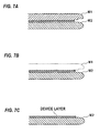
- the vertical surface and the horizontal surface, which have been formed by the first polishing tape 3A, are removed by a grinder. More specifically, as illustrated in FIG. 7A and FIG. 7B , a device substrate W1, which has been polished by the polishing apparatus according to the embodiment, and a silicon substrate W2 are stuck together, and a back side of the device substrate W1 is scraped away by the grinder. As a result, the SOI substrate as illustrated in FIG. 7C is obtained. Only a smooth vertical surface, which has been formed by the second polishing tape 3B having the fine polishing surface, remains on the device substrate W1.
- SOI Silicon on Insulator
Landscapes
- Engineering & Computer Science (AREA)
- Mechanical Engineering (AREA)
- Chemical & Material Sciences (AREA)
- Ceramic Engineering (AREA)
- Inorganic Chemistry (AREA)
- Physics & Mathematics (AREA)
- Condensed Matter Physics & Semiconductors (AREA)
- General Physics & Mathematics (AREA)
- Manufacturing & Machinery (AREA)
- Computer Hardware Design (AREA)
- Microelectronics & Electronic Packaging (AREA)
- Power Engineering (AREA)
- Mechanical Treatment Of Semiconductor (AREA)
- Grinding And Polishing Of Tertiary Curved Surfaces And Surfaces With Complex Shapes (AREA)
- Finish Polishing, Edge Sharpening, And Grinding By Specific Grinding Devices (AREA)
Abstract
Description
- Field of the Invention:
- The present invention relates to a method of polishing a substrate, such as a wafer. More particularly, the present invention relates to a method of polishing an edge portion of a substrate by pressing a polishing tool against the edge portion.
- Description of the Related Art:
- A polishing apparatus, which has a polishing tool (e.g., a polishing tape or a fixed abrasive), is used for polishing a peripheral portion of a wafer. This type of polishing apparatus is configured to bring the polishing tool into contact with the peripheral portion of the wafer, while rotating the wafer, to thereby polish the peripheral portion of the wafer. In this specification, the peripheral portion of the wafer is defined as a region including a bevel portion which is the outermost portion of the wafer and a top edge portion and a bottom edge portion located radially inwardly of the bevel portion.
-
FIG. 8A and FIG. 8B are enlarged cross-sectional views each showing the peripheral portion of the wafer. More specifically,FIG. 8A shows a cross-sectional view of a so-called straight-type wafer, andFIG. 8B shows a cross-sectional view of a so-called round-type wafer. In the wafer W shown inFIG. 8A , the bevel portion is an outermost circumferential surface of the wafer W (indicated by a symbol B) that is constituted by an upper slope (an upper bevel portion) P, a lower slope (a lower bevel portion) Q, and a side portion (an apex) R. In the wafer W shown inFIG. 8B , the bevel portion is a portion (indicated by a symbol B) having a curved cross section and constituting an outermost circumferential surface of the wafer W. The top edge portion is a flat portion E1 located radially inwardly of the bevel portion B. The bottom edge portion is a flat portion E2 located opposite the top edge portion and located radially inwardly of the bevel portion B. The top edge portion E1 and the bottom edge portion E2 may be collectively referred to as edge portion. The edge portion may include a region where devices are formed. - In a fabrication process of SOI (Silicon on Insulator) substrate, there is a need to form a vertical surface and a horizontal surface on the edge portion of the wafer W, as shown in
FIG. 9 . The SOI substrate is manufactured by sticking a device substrate and a silicon substrate together. More specifically, as illustrated inFIG. 10A and FIG. 10B , a device substrate W1 and a silicon substrate W2 are stuck together, and as illustrated inFIG. 10C , a back side of the device substrate W1 is scraped away by a grinder. As a result, the SOI substrate as illustrated inFIG. 10D is obtained. - A cross section of the edge portion as illustrated in
FIG. 9 can be formed with use of a polishing apparatus shown inFIG. 11 . Specifically, while a wafer W is rotated, a pressingmember 100 presses an edge of apolishing tape 101 downwardly against the edge portion of the wafer W to thereby polish the edge portion of the wafer W. Thepolishing tape 101 has its lower surface serving as a polishing surface that holds abrasive grains thereon. This polishing surface is disposed parallel to the wafer W. With the edge of thepolishing tape 101 located on the edge portion of the wafer W, thepressing member 100 presses the polishing surface of thepolishing tape 101 against the edge portion of the wafer W to thereby form a right-angled cross section as shown inFIG. 9 , i.e., the vertical surface and the horizontal surface on the edge portion of the wafer W. - In order to increase a throughput of the polishing apparatus shown in
FIG. 11 , it is preferable to use a polishing tape having a more abrasive or rough polishing surface. This is because a polishing rate (which is also referred to as a removal rate) of the wafer W is increased. However, use of the polishing tape having the rough polishing surface may roughen the vertical surface of the edge portion of the wafer W. Moreover, the edge portion of the wafer W may become chipped. Use of a polishing tape having a less abrasive or fine polishing surface can form a smooth vertical surface on the edge portion of the wafer W. However, the use of the polishing tape having the fine polishing surface may result in a lowered polishing rate of the wafer W. - In an embodiment an apparatus is used to polish a substrate. This apparatus is used to rotate a substrate; press a first polishing tool against an edge portion of the substrate to polish the edge portion; and press a second polishing tool against the edge portion of the substrate to polish the edge portion. The second polishing tool is preferably located more inwardly than the first polishing tool with respect to a radial direction of the substrate. The first polishing tool has a polishing surface more abrasive than a polishing surface of the second polishing tool.
- According to the above-described embodiment, the first polishing tool first polishes the edge portion of the substrate. Therefore, a contact area between the second polishing tool and the edge portion becomes small, and as a result pressure of the second polishing tool applied to the edge portion is increased. Accordingly, the second polishing tool having a finer polishing surface than the first polishing tool can polish the edge portion of the substrate at a high polishing rate (i.e., a high removal rate). Moreover, the second polishing tool having the fine polishing surface can form a smooth vertical surface on the edge portion of the substrate.
-
-
FIG. 1 is a schematic view of a polishing apparatus for carrying out an embodiment of polishing a substrate; -
FIG. 2 is a plan view of the polishing apparatus shown inFIG. 1 ; -
FIG. 3 is a side view showing a state in which a pressing pad is pressing a first polishing tape against an edge portion of a wafer to polish the edge portion of the wafer; -
FIG. 4 is a diagram illustrating an arrangement of the first polishing tape and a second polishing tape; -
FIG. 5A, FIG. 5B, and FIG. 5C are views each showing an embodiment of the polishing method; -
FIG. 6 is a view illustrating a manner of polishing the edge portion of the wafer with use of a single polishing tape; -
FIG. 7A, FIG. 7B, and FIG. 7C are diagrams showing a process of fabricating an SOI (Silicon on Insulator) substrate using a substrate that has been polished by the polishing apparatus according to the embodiment; -
FIG. 8A and FIG. 8B are cross-sectional views each showing a peripheral portion of a wafer; -
FIG. 9 is a view showing a vertical surface and a horizontal surface formed on the edge portion of the wafer; -
FIG. 10A, FIG. 10B, FIG. 10C, and FIG. 10D are diagrams showing a process of fabricating an SOI substrate; and -
FIG. 11 is a diagram showing an example of a polishing apparatus that can form a cross section of the edge portion as illustrated inFIG. 9 . - An embodiment will now be described in detail with reference to the drawings.
-
FIG. 1 is a schematic view illustrating a polishing apparatus for carrying out an embodiment of a polishing method, andFIG. 2 is a plan view of the polishing apparatus shown inFIG. 1 . The polishing apparatus has asubstrate holder 1 for holding and rotating a wafer W which is an example of a substrate, afirst polishing unit 2A and asecond polishing unit 2B for polishing an edge portion of the wafer W when held by thesubstrate holder 1, and a polishing liquid supply mechanism 4 for supplying a polishing liquid (e.g., pure water) onto a central portion of the wafer W. - An arrangement of the two polishing
units substrate holder 1. Thefirst polishing unit 2A is configured to place afirst polishing tape 3A, which is a first polishing tool, in sliding contact with the edge portion of the wafer W to thereby polish the edge portion, and thesecond polishing unit 2B is configured to place asecond polishing tape 3B, which is a second polishing tool, in sliding contact with the edge portion of the wafer W to thereby polish the edge portion. Thefirst polishing tape 3A has a polishing surface rougher than a polishing surface of thesecond polishing tape 3B. During polishing of the wafer W, the polishing liquid is supplied from the polishing liquid supply mechanism 4 onto the central portion of the wafer W. Examples of the polishing liquid to be used include pure water. Instead of the polishing tape, a grindstone (or a fixed abrasive) may be used as the first polishing tool and/or the second polishing tool. - Since the
first polishing unit 2A and thesecond polishing unit 2B have the same structure, thefirst polishing unit 2A will be described below. Thefirst polishing unit 2A includes a polishing-tape support mechanism (a polishing-tool support mechanism) 5 for supporting thefirst polishing tape 3A, a pressing pad (a pressing member) 7 for pressing thefirst polishing tape 3A downwardly against the edge portion of the wafer W, a vertically movingmechanism 9 for moving thepressing pad 7 in a direction perpendicular to the wafer surface, a pressing-pad moving mechanism (a pressing-member moving mechanism) 10 for moving thepressing pad 7 and the vertically movingmechanism 9 in a radial direction of the wafer W, and a tape moving mechanism (a polishing-tool moving mechanism) 11 for moving thefirst polishing tape 3A and the polishing-tape support mechanism 5 in the radial direction of the wafer W. - The pressing-
pad moving mechanism 10 and thetape moving mechanism 11 are operable independently of each other. Therefore, a relative position of thepressing pad 7 and thefirst polishing tape 3A in the radial direction of the wafer W can be adjusted by the pressing-pad moving mechanism 10 and thetape moving mechanism 11. A combination of pneumatic cylinders, a combination of a servomotor and a ball screw, or the like can be used as the vertically movingmechanism 9, the pressing-pad moving mechanism 10, and thetape moving mechanism 11. - The polishing-
tape support mechanism 5 includes a feedingreel 12 for feeding thefirst polishing tape 3A to thepressing pad 7 and a take-up reel 14 for taking up thefirst polishing tape 3A. Thefirst polishing tape 3A extends from the feedingreel 12 to the take-up reel 14 via thepressing pad 7. Thefirst polishing tape 3A is supported by the polishing-tape support mechanism 5 such that the polishing surface of thefirst polishing tape 3A lies parallel to the surface of the wafer W and the polishing surface faces the edge portion of the wafer W. - One surface (a lower surface) of the
first polishing tape 3A constitutes the polishing surface having abrasive grains fixed thereto. Thefirst polishing tape 3A is a long polishing tool, and is disposed along a tangential direction of the wafer W. Thepressing pad 7 is a pressing member for pressing thefirst polishing tape 3A against the edge portion of the wafer W, and is disposed above the edge portion of the wafer W. Thefirst polishing tape 3A is located between thepressing pad 7 and the edge portion of the wafer W.A tape stopper 17 for restricting an outward movement of thefirst polishing tape 3A is fixed to a bottom of thepressing pad 7. Thistape stopper 17 may be omitted. -
FIG. 3 is a side view showing a state in which thepressing pad 7 is pressing thefirst polishing tape 3A against the edge portion of the wafer W to polish the edge portion of the wafer W. Thefirst polishing unit 2A polishes the edge portion of the wafer W with the use of thefirst polishing tape 3A. Similarly, thesecond polishing unit 2B polishes the edge portion of the wafer W with the use of thesecond polishing tape 3B which is different from thefirst polishing tape 3A. Thefirst polishing tape 3A has the polishing surface which is rougher than the polishing surface of the polishingtape 3B. For example, thefirst polishing tape 3A is a polishing tape having a rough polishing surface for rough-polishing of the wafer, while thesecond polishing tape 3B is a polishing tape having a fine polishing surface for finish-polishing of the wafer. - As shown in
FIG. 4 , thesecond polishing tape 3B and thepressing pad 7 of thesecond polishing unit 2B are located more inwardly than thefirst polishing tape 3A and thepressing pad 7 of thefirst polishing unit 2A with respect to the radial direction of the wafer W. More specifically, as shown inFIG. 4 , a distance L1 between an inner edge of thefirst polishing tape 3A and the outermost periphery of the wafer W is shorter than a distance L2 between an inner edge of thesecond polishing tape 3B and the outermost periphery of the wafer W. Therefore, thesecond polishing tape 3B polishes a region in the edge portion lying radially inwardly of thefirst polishing tape 3A. -
FIG. 5A through FIG. 5C are views each showing an embodiment of the polishing method. The wafer W is rotated about its axis by the substrate holder 1 (seeFIG. 1 andFIG. 2 ). In this state, as shown inFIG. 5A , thefirst polishing tape 3A is firstly brought into contact with the edge portion of the wafer W to start polishing of the edge portion. At this time, thesecond polishing tape 3B is located away from the wafer W. After a predetermined time has elapsed from a time when thefirst polishing tape 3A is brought into contact with the wafer W (i.e., a time when thefirst polishing tape 3A starts polishing of the edge portion of the wafer W), thesecond polishing tape 3B is brought into contact with the edge portion of the wafer W to start polishing of the edge portion, as shown inFIG. 5B . Further, as shown inFIG. 5C , thepressing pads units first polishing tape 3A and thesecond polishing tape 3B against the edge portion of the wafer W, thereby forming vertical surfaces and horizontal surfaces on the edge portion of the wafer W. Although not shown inFIG. 5A through FIG. 5C , the polishing liquid is supplied from the polishing liquid supply mechanism 4 onto the upper surface of the wafer W. - Each
pressing pad 7 has a wafer pressing surface (i.e., a substrate pressing surface) which is a horizontal surface parallel to the wafer surface. The polishingunits tapes tapes - As can be seen from
FIG. 5C , thefirst polishing tape 3A is firstly started to polish an outer region of the edge portion of the wafer W, and subsequently thesecond polishing tape 3B is started to polish an inner region of the edge portion of the wafer W. A contact width P1 of thefirst polishing tape 3A when contacting the edge portion may preferably be equal to or larger than a contact width P2 of thesecond polishing tape 3B when contacting the edge portion. This is for reducing a contact area between thesecond polishing tape 3B and the edge portion of the wafer W so as to increase a polishing pressure of thesecond polishing tape 3B applied to the edge portion of the wafer W. The above-described contact width is a contact width in the radial direction of the wafer W. - In order to allow the
first polishing tape 3A to polish the edge portion of the wafer ahead of thesecond polishing tape 3B throughout the polishing of the wafer, a removal rate (or a polishing rate) of the edge portion polished by thefirst polishing tape 3A is preferably higher than a removal rate (or a polishing rate) of the edge portion polished by thesecond polishing tape 3B. -
FIG. 6 is a view illustrating a manner of polishing the edge portion of the wafer W with use of asingle polishing tape 20. As can be seen from a comparison betweenFIG. 6 andFIG. 5C , the contact area between thefirst polishing tape 3A and the wafer W and the contact area between thesecond polishing tape 3B and the wafer W are smaller than a contact area between the wafer W and the polishingtape 20 shown inFIG. 6 . This means that pressure of each of thefirst polishing tape 3A and thesecond polishing tape 3B exerted on the wafer W is higher than pressure of the polishingtape 20 exerted on the wafer W. Therefore, thefirst polishing tape 3A and thesecond polishing tape 3B can polish the edge portion of the wafer W at a high polishing rate. - In a fabrication process of an SOI (Silicon on Insulator) substrate, the vertical surface and the horizontal surface, which have been formed by the
first polishing tape 3A, are removed by a grinder. More specifically, as illustrated inFIG. 7A and FIG. 7B , a device substrate W1, which has been polished by the polishing apparatus according to the embodiment, and a silicon substrate W2 are stuck together, and a back side of the device substrate W1 is scraped away by the grinder. As a result, the SOI substrate as illustrated inFIG. 7C is obtained. Only a smooth vertical surface, which has been formed by thesecond polishing tape 3B having the fine polishing surface, remains on the device substrate W1. - The previous description of embodiments is provided to enable a person skilled in the art to make and use the present invention. Moreover, various modifications to these embodiments will be readily apparent to those skilled in the art, and the generic principles and specific examples defined herein may be applied to other embodiments. Therefore, the present invention is not intended to be limited to the embodiments described herein but is to be accorded the widest scope as defined by limitation of the claims and equivalents.
Claims (14)
- A method of manufacturing a semiconductor, comprising:rotating a semiconductor wafer;applying a first polishing tool against an edge portion of the semiconductor wafer to polish the edge portion; andapplying a second polishing tool against the edge portion of the semiconductor wafer to polish the edge portion, the second polishing tool being located more inwardly than the first polishing tool with respect to a radial direction of the semiconductor wafer,the first polishing tool having a polishing surface more abrasive than a polishing surface of the second polishing tool.
- The method of manufacturing a semiconductor according to claim 1, further comprising:bringing the second polishing tool into contact with the edge portion of the semiconductor wafer after a predetermined time has elapsed from a time when the first polishing tool is brought into contact with the edge portion of the substrate.
- The method of manufacturing a semiconductor according to claim 1, wherein a contact width of the first polishing tool when contacting the edge portion of the semiconductor wafer is equal to or larger than a contact width of the second polishing tool when contacting the edge portion of the semiconductor wafer.
- The method of manufacturing a semiconductor according to claim 1, wherein a removal rate of the edge portion polished by the first polishing tool is higher than a removal rate of the edge portion polished by the second polishing tool.
- The method of manufacturing a semiconductor according to claim 1, wherein the first polishing tool is a polishing tool for rough-polishing of the semiconductor wafer, and the second polishing tool is a polishing tool for finish-polishing of the semiconductor wafer.
- The method of manufacturing a semiconductor according to claim 1, wherein at least one of the first polishing tool and the second polishing tool comprises a polishing tape or a grindstone.
- A substrate polishing apparatus, comprising:a substrate holder configured to rotate the substrate;a first polishing tool configured to press against an edge portion of the substrate to polish the edge portion; anda second polishing tool configured to press against the edge portion of the substrate to polish the edge portion, the second polishing tool being located more inwardly than the first polishing tool with respect to a radial direction of the substrate,the first polishing tool having a polishing surface more abrasive than a polishing surface of the second polishing tool.
- The substrate polishing apparatus according to claim 7, further comprising:the second polishing tool configured for contact with the edge portion of the substrate after a predetermined time has elapsed from a time when the first polishing tool is configured for contact with the edge portion of the substrate.
- The substrate polishing apparatus according to claim 7, wherein a contact width of the first polishing tool when contacting the edge portion of the substrate is equal to or larger than a contact width of the second polishing tool when contacting the edge portion of the substrate.
- The substrate polishing apparatus according to claim 7, wherein the first polishing tool is configured for a removal rate of the substrate that is higher than a removal rate of the substrate by the second polishing tool.
- The substrate polishing apparatus according to claim 7, wherein the first polishing tool is configured as a polishing tool for rough-polishing of the substrate, and the second polishing tool is configured as a polishing tool for finish-polishing of the substrate.
- The substrate polishing apparatus according to claim 7, wherein at least one of the first polishing tool and the second polishing tool comprises a polishing tape.
- The substrate polishing apparatus according to claim 7, wherein at least one of the first polishing tool and the second polishing tool comprises a grindstone.
- A method of manufacturing a semiconductor, comprising:rotating a substrate;pressing a first polishing tool against an edge portion of the substrate to polish the edge portion; andpressing a second polishing tool against the edge portion of the substrate to polish the edge portion, the second polishing tool being located more inwardly than the first polishing tool with respect to a radial direction of the substrate,the first polishing tool having a polishing surface rougher than a polishing surface of the second polishing tool.
Applications Claiming Priority (1)
| Application Number | Priority Date | Filing Date | Title |
|---|---|---|---|
| JP2013015937A JP6100541B2 (en) | 2013-01-30 | 2013-01-30 | Polishing method |
Publications (3)
| Publication Number | Publication Date |
|---|---|
| EP2762272A2 true EP2762272A2 (en) | 2014-08-06 |
| EP2762272A3 EP2762272A3 (en) | 2017-12-06 |
| EP2762272B1 EP2762272B1 (en) | 2023-03-08 |
Family
ID=50033327
Family Applications (1)
| Application Number | Title | Priority Date | Filing Date |
|---|---|---|---|
| EP14020009.8A Active EP2762272B1 (en) | 2013-01-30 | 2014-01-28 | Wafer polishing apparatus and method |
Country Status (6)
| Country | Link |
|---|---|
| US (2) | US9399274B2 (en) |
| EP (1) | EP2762272B1 (en) |
| JP (2) | JP6100541B2 (en) |
| KR (1) | KR101798700B1 (en) |
| CN (1) | CN103962918A (en) |
| TW (2) | TWI623033B (en) |
Cited By (1)
| Publication number | Priority date | Publication date | Assignee | Title |
|---|---|---|---|---|
| KR20200010073A (en) * | 2018-07-20 | 2020-01-30 | 가부시키가이샤 에바라 세이사꾸쇼 | Polishing apparatus and polishing method |
Families Citing this family (13)
| Publication number | Priority date | Publication date | Assignee | Title |
|---|---|---|---|---|
| TWI663025B (en) * | 2012-09-24 | 2019-06-21 | 日商荏原製作所股份有限公司 | Grinding method and grinding device |
| JP5889760B2 (en) | 2012-09-24 | 2016-03-22 | 株式会社荏原製作所 | Substrate polishing abnormality detection method and polishing apparatus |
| JP6204848B2 (en) * | 2014-02-17 | 2017-09-27 | 株式会社荏原製作所 | Polishing apparatus and polishing method |
| JP6908464B2 (en) * | 2016-09-15 | 2021-07-28 | 株式会社荏原製作所 | Substrate processing method and substrate processing equipment |
| JP6920849B2 (en) * | 2017-03-27 | 2021-08-18 | 株式会社荏原製作所 | Substrate processing method and equipment |
| TWI725225B (en) * | 2017-08-30 | 2021-04-21 | 日商荏原製作所股份有限公司 | Grinding device and grinding method |
| JP6877585B2 (en) * | 2017-12-19 | 2021-05-26 | 東京エレクトロン株式会社 | Board processing system, board processing method and computer storage medium |
| CN108161702B (en) * | 2018-03-16 | 2019-09-06 | 中国工程物理研究院激光聚变研究中心 | A kind of polishing machine |
| JP2020028928A (en) * | 2018-08-21 | 2020-02-27 | 株式会社荏原製作所 | Processing method and processing apparatus |
| JP7562994B2 (en) * | 2020-06-08 | 2024-10-08 | 株式会社Sumco | Wafer outer circumference polishing device |
| JP2022063417A (en) * | 2020-10-12 | 2022-04-22 | 株式会社荏原製作所 | Substrate cleaning device and substrate cleaning method |
| TWI756939B (en) * | 2020-11-25 | 2022-03-01 | 友達光電股份有限公司 | Substrate device, display panel and manufactory method thereof |
| CN114161289B (en) * | 2021-12-10 | 2022-12-13 | 阜南县德盛隆工艺家具有限公司 | Polisher is used in processing of bamboo weaving handicraft |
Family Cites Families (19)
| Publication number | Priority date | Publication date | Assignee | Title |
|---|---|---|---|---|
| JPH074747B2 (en) * | 1986-03-17 | 1995-01-25 | ニトマック・イーアール株式会社 | Method and apparatus for grinding outer peripheral surface of hard and brittle material |
| JPH04263425A (en) * | 1991-02-18 | 1992-09-18 | Toshiba Corp | Grinding device for semiconductor substrate and method thereof |
| JPH0897111A (en) * | 1994-09-26 | 1996-04-12 | Kyushu Komatsu Denshi Kk | Method for manufacturing soi substrate |
| JP3197253B2 (en) * | 1998-04-13 | 2001-08-13 | 株式会社日平トヤマ | Wafer chamfering method |
| JP2001205549A (en) * | 2000-01-25 | 2001-07-31 | Speedfam Co Ltd | One side polishing method and device for substrate edge portion |
| JP2002025952A (en) * | 2000-07-07 | 2002-01-25 | Disco Abrasive Syst Ltd | Treatment method of semiconductor wafer |
| JP2002030275A (en) * | 2000-07-17 | 2002-01-31 | Nihon Micro Coating Co Ltd | Texture processing fluid and method therefor |
| JP2004103825A (en) * | 2002-09-10 | 2004-04-02 | Nihon Micro Coating Co Ltd | Device and method for grinding semiconductor wafer edge |
| JP4125148B2 (en) * | 2003-02-03 | 2008-07-30 | 株式会社荏原製作所 | Substrate processing equipment |
| US20070270084A1 (en) * | 2004-08-17 | 2007-11-22 | Showa Denko K.K. | Method of Manufacturing Silicon Substrates for Magnetic Recording Medium, Silicon Substrate for Magnetic Recording Medium, Magnetic Recording Medium, and Magnetic Recording Apparatus |
| JP5119614B2 (en) * | 2006-06-13 | 2013-01-16 | 株式会社東京精密 | Wafer outer periphery grinding method |
| JP5274993B2 (en) * | 2007-12-03 | 2013-08-28 | 株式会社荏原製作所 | Polishing equipment |
| KR101578956B1 (en) * | 2008-02-22 | 2015-12-18 | 니혼 미크로 코팅 가부시끼 가이샤 | Method and apparatus for polishing outer circumferential end section of semiconductor wafer |
| JP5352331B2 (en) * | 2009-04-15 | 2013-11-27 | ダイトエレクトロン株式会社 | Wafer chamfering method |
| JP5663295B2 (en) * | 2010-01-15 | 2015-02-04 | 株式会社荏原製作所 | Polishing apparatus, polishing method, and pressing member for pressing a polishing tool |
| JP5571409B2 (en) * | 2010-02-22 | 2014-08-13 | 株式会社荏原製作所 | Manufacturing method of semiconductor device |
| US8540551B2 (en) * | 2010-12-15 | 2013-09-24 | Corning Incorporated | Glass edge finish system, belt assembly, and method for using same |
| JP2012204545A (en) | 2011-03-24 | 2012-10-22 | Toshiba Corp | Manufacturing method of semiconductor device and manufacturing apparatus |
| JP5886602B2 (en) | 2011-03-25 | 2016-03-16 | 株式会社荏原製作所 | Polishing apparatus and polishing method |
-
2013
- 2013-01-30 JP JP2013015937A patent/JP6100541B2/en active Active
-
2014
- 2014-01-27 KR KR1020140009540A patent/KR101798700B1/en active IP Right Grant
- 2014-01-28 TW TW106128761A patent/TWI623033B/en active
- 2014-01-28 EP EP14020009.8A patent/EP2762272B1/en active Active
- 2014-01-28 TW TW103103082A patent/TWI601195B/en active
- 2014-01-29 CN CN201410043731.4A patent/CN103962918A/en active Pending
- 2014-01-29 US US14/167,898 patent/US9399274B2/en active Active
-
2016
- 2016-06-21 US US15/188,638 patent/US9604335B2/en active Active
-
2017
- 2017-02-23 JP JP2017031756A patent/JP6401319B2/en active Active
Cited By (1)
| Publication number | Priority date | Publication date | Assignee | Title |
|---|---|---|---|---|
| KR20200010073A (en) * | 2018-07-20 | 2020-01-30 | 가부시키가이샤 에바라 세이사꾸쇼 | Polishing apparatus and polishing method |
Also Published As
| Publication number | Publication date |
|---|---|
| US20140213155A1 (en) | 2014-07-31 |
| KR20140097995A (en) | 2014-08-07 |
| US9604335B2 (en) | 2017-03-28 |
| KR101798700B1 (en) | 2017-11-16 |
| JP2017094487A (en) | 2017-06-01 |
| JP2014144525A (en) | 2014-08-14 |
| JP6100541B2 (en) | 2017-03-22 |
| TWI623033B (en) | 2018-05-01 |
| TWI601195B (en) | 2017-10-01 |
| US9399274B2 (en) | 2016-07-26 |
| TW201434083A (en) | 2014-09-01 |
| EP2762272B1 (en) | 2023-03-08 |
| TW201743378A (en) | 2017-12-16 |
| CN103962918A (en) | 2014-08-06 |
| EP2762272A3 (en) | 2017-12-06 |
| JP6401319B2 (en) | 2018-10-10 |
| US20160297048A1 (en) | 2016-10-13 |
Similar Documents
| Publication | Publication Date | Title |
|---|---|---|
| US9604335B2 (en) | Wafer polishing apparatus | |
| US9293318B2 (en) | Semiconductor wafer manufacturing method | |
| TWI585838B (en) | Method of polishing back surface of substrate and substrate processing apparatus | |
| TW393369B (en) | A wafer processing machine and a processing method thereby | |
| JP6963075B2 (en) | Wafer surface treatment equipment | |
| KR100832768B1 (en) | Wafer polishing apparatus and method for polishing wafers | |
| JP6345988B2 (en) | Substrate processing equipment | |
| TWI523096B (en) | Wafer polishing tool and method for wafer polishing | |
| JP2008042220A (en) | Method and apparatus for processing substrate | |
| US20200258735A1 (en) | Wafer polishing method and apparatus | |
| JP4103808B2 (en) | Wafer grinding method and wafer | |
| JP6717706B2 (en) | Wafer surface treatment equipment | |
| JP2002355748A (en) | Chemical-mechanical polishing method and chemical- mechanical polishing device | |
| JP2018056500A (en) | Method for processing plate-like object | |
| JP6941420B2 (en) | Wafer surface treatment equipment | |
| JP6843554B2 (en) | Wafer surface treatment equipment | |
| KR20170038434A (en) | Chemical mechanical polishing apparatus for substrate | |
| JP5484172B2 (en) | Method for forming tapered surface of polishing pad | |
| JP6698475B2 (en) | Wafer surface treatment equipment | |
| JP2017127938A (en) | Wafer polishing method, back pad manufacturing method, back pad, and polishing head having the back pad | |
| JP2016066724A (en) | Wafer polishing method | |
| KR20150086008A (en) | Grooved polishing pad for wafer |
Legal Events
| Date | Code | Title | Description |
|---|---|---|---|
| PUAI | Public reference made under article 153(3) epc to a published international application that has entered the european phase |
Free format text: ORIGINAL CODE: 0009012 |
|
| 17P | Request for examination filed |
Effective date: 20140128 |
|
| AK | Designated contracting states |
Kind code of ref document: A2 Designated state(s): AL AT BE BG CH CY CZ DE DK EE ES FI FR GB GR HR HU IE IS IT LI LT LU LV MC MK MT NL NO PL PT RO RS SE SI SK SM TR |
|
| AX | Request for extension of the european patent |
Extension state: BA ME |
|
| PUAL | Search report despatched |
Free format text: ORIGINAL CODE: 0009013 |
|
| AK | Designated contracting states |
Kind code of ref document: A3 Designated state(s): AL AT BE BG CH CY CZ DE DK EE ES FI FR GB GR HR HU IE IS IT LI LT LU LV MC MK MT NL NO PL PT RO RS SE SI SK SM TR |
|
| AX | Request for extension of the european patent |
Extension state: BA ME |
|
| RIC1 | Information provided on ipc code assigned before grant |
Ipc: B24B 9/06 20060101AFI20171027BHEP Ipc: B24B 21/06 20060101ALI20171027BHEP Ipc: B24B 21/00 20060101ALI20171027BHEP |
|
| STAA | Information on the status of an ep patent application or granted ep patent |
Free format text: STATUS: REQUEST FOR EXAMINATION WAS MADE |
|
| R17P | Request for examination filed (corrected) |
Effective date: 20180518 |
|
| RBV | Designated contracting states (corrected) |
Designated state(s): AL AT BE BG CH CY CZ DE DK EE ES FI FR GB GR HR HU IE IS IT LI LT LU LV MC MK MT NL NO PL PT RO RS SE SI SK SM TR |
|
| STAA | Information on the status of an ep patent application or granted ep patent |
Free format text: STATUS: EXAMINATION IS IN PROGRESS |
|
| 17Q | First examination report despatched |
Effective date: 20210521 |
|
| STAA | Information on the status of an ep patent application or granted ep patent |
Free format text: STATUS: EXAMINATION IS IN PROGRESS |
|
| REG | Reference to a national code |
Ref country code: DE Ref legal event code: R079 Ref document number: 602014086392 Country of ref document: DE Free format text: PREVIOUS MAIN CLASS: B24B0009060000 Ipc: B24B0027000000 |
|
| RIC1 | Information provided on ipc code assigned before grant |
Ipc: B24B 21/00 20060101ALI20220715BHEP Ipc: B24B 21/06 20060101ALI20220715BHEP Ipc: B24B 9/06 20060101ALI20220715BHEP Ipc: B24B 27/00 20060101AFI20220715BHEP |
|
| GRAP | Despatch of communication of intention to grant a patent |
Free format text: ORIGINAL CODE: EPIDOSNIGR1 |
|
| STAA | Information on the status of an ep patent application or granted ep patent |
Free format text: STATUS: GRANT OF PATENT IS INTENDED |
|
| INTG | Intention to grant announced |
Effective date: 20220915 |
|
| GRAS | Grant fee paid |
Free format text: ORIGINAL CODE: EPIDOSNIGR3 |
|
| GRAA | (expected) grant |
Free format text: ORIGINAL CODE: 0009210 |
|
| STAA | Information on the status of an ep patent application or granted ep patent |
Free format text: STATUS: THE PATENT HAS BEEN GRANTED |
|
| AK | Designated contracting states |
Kind code of ref document: B1 Designated state(s): AL AT BE BG CH CY CZ DE DK EE ES FI FR GB GR HR HU IE IS IT LI LT LU LV MC MK MT NL NO PL PT RO RS SE SI SK SM TR |
|
| REG | Reference to a national code |
Ref country code: GB Ref legal event code: FG4D |
|
| REG | Reference to a national code |
Ref country code: CH Ref legal event code: EP Ref country code: AT Ref legal event code: REF Ref document number: 1552264 Country of ref document: AT Kind code of ref document: T Effective date: 20230315 |
|
| REG | Reference to a national code |
Ref country code: IE Ref legal event code: FG4D |
|
| REG | Reference to a national code |
Ref country code: DE Ref legal event code: R096 Ref document number: 602014086392 Country of ref document: DE |
|
| REG | Reference to a national code |
Ref country code: LT Ref legal event code: MG9D |
|
| P01 | Opt-out of the competence of the unified patent court (upc) registered |
Effective date: 20230528 |
|
| REG | Reference to a national code |
Ref country code: NL Ref legal event code: MP Effective date: 20230308 |
|
| PG25 | Lapsed in a contracting state [announced via postgrant information from national office to epo] |
Ref country code: RS Free format text: LAPSE BECAUSE OF FAILURE TO SUBMIT A TRANSLATION OF THE DESCRIPTION OR TO PAY THE FEE WITHIN THE PRESCRIBED TIME-LIMIT Effective date: 20230308 Ref country code: NO Free format text: LAPSE BECAUSE OF FAILURE TO SUBMIT A TRANSLATION OF THE DESCRIPTION OR TO PAY THE FEE WITHIN THE PRESCRIBED TIME-LIMIT Effective date: 20230608 Ref country code: LV Free format text: LAPSE BECAUSE OF FAILURE TO SUBMIT A TRANSLATION OF THE DESCRIPTION OR TO PAY THE FEE WITHIN THE PRESCRIBED TIME-LIMIT Effective date: 20230308 Ref country code: LT Free format text: LAPSE BECAUSE OF FAILURE TO SUBMIT A TRANSLATION OF THE DESCRIPTION OR TO PAY THE FEE WITHIN THE PRESCRIBED TIME-LIMIT Effective date: 20230308 Ref country code: HR Free format text: LAPSE BECAUSE OF FAILURE TO SUBMIT A TRANSLATION OF THE DESCRIPTION OR TO PAY THE FEE WITHIN THE PRESCRIBED TIME-LIMIT Effective date: 20230308 Ref country code: ES Free format text: LAPSE BECAUSE OF FAILURE TO SUBMIT A TRANSLATION OF THE DESCRIPTION OR TO PAY THE FEE WITHIN THE PRESCRIBED TIME-LIMIT Effective date: 20230308 |
|
| REG | Reference to a national code |
Ref country code: AT Ref legal event code: MK05 Ref document number: 1552264 Country of ref document: AT Kind code of ref document: T Effective date: 20230308 |
|
| PG25 | Lapsed in a contracting state [announced via postgrant information from national office to epo] |
Ref country code: SE Free format text: LAPSE BECAUSE OF FAILURE TO SUBMIT A TRANSLATION OF THE DESCRIPTION OR TO PAY THE FEE WITHIN THE PRESCRIBED TIME-LIMIT Effective date: 20230308 Ref country code: NL Free format text: LAPSE BECAUSE OF FAILURE TO SUBMIT A TRANSLATION OF THE DESCRIPTION OR TO PAY THE FEE WITHIN THE PRESCRIBED TIME-LIMIT Effective date: 20230308 Ref country code: GR Free format text: LAPSE BECAUSE OF FAILURE TO SUBMIT A TRANSLATION OF THE DESCRIPTION OR TO PAY THE FEE WITHIN THE PRESCRIBED TIME-LIMIT Effective date: 20230609 Ref country code: FI Free format text: LAPSE BECAUSE OF FAILURE TO SUBMIT A TRANSLATION OF THE DESCRIPTION OR TO PAY THE FEE WITHIN THE PRESCRIBED TIME-LIMIT Effective date: 20230308 |
|
| PG25 | Lapsed in a contracting state [announced via postgrant information from national office to epo] |
Ref country code: SM Free format text: LAPSE BECAUSE OF FAILURE TO SUBMIT A TRANSLATION OF THE DESCRIPTION OR TO PAY THE FEE WITHIN THE PRESCRIBED TIME-LIMIT Effective date: 20230308 Ref country code: RO Free format text: LAPSE BECAUSE OF FAILURE TO SUBMIT A TRANSLATION OF THE DESCRIPTION OR TO PAY THE FEE WITHIN THE PRESCRIBED TIME-LIMIT Effective date: 20230308 Ref country code: PT Free format text: LAPSE BECAUSE OF FAILURE TO SUBMIT A TRANSLATION OF THE DESCRIPTION OR TO PAY THE FEE WITHIN THE PRESCRIBED TIME-LIMIT Effective date: 20230710 Ref country code: EE Free format text: LAPSE BECAUSE OF FAILURE TO SUBMIT A TRANSLATION OF THE DESCRIPTION OR TO PAY THE FEE WITHIN THE PRESCRIBED TIME-LIMIT Effective date: 20230308 Ref country code: CZ Free format text: LAPSE BECAUSE OF FAILURE TO SUBMIT A TRANSLATION OF THE DESCRIPTION OR TO PAY THE FEE WITHIN THE PRESCRIBED TIME-LIMIT Effective date: 20230308 Ref country code: AT Free format text: LAPSE BECAUSE OF FAILURE TO SUBMIT A TRANSLATION OF THE DESCRIPTION OR TO PAY THE FEE WITHIN THE PRESCRIBED TIME-LIMIT Effective date: 20230308 |
|
| PG25 | Lapsed in a contracting state [announced via postgrant information from national office to epo] |
Ref country code: SK Free format text: LAPSE BECAUSE OF FAILURE TO SUBMIT A TRANSLATION OF THE DESCRIPTION OR TO PAY THE FEE WITHIN THE PRESCRIBED TIME-LIMIT Effective date: 20230308 Ref country code: PL Free format text: LAPSE BECAUSE OF FAILURE TO SUBMIT A TRANSLATION OF THE DESCRIPTION OR TO PAY THE FEE WITHIN THE PRESCRIBED TIME-LIMIT Effective date: 20230308 Ref country code: IS Free format text: LAPSE BECAUSE OF FAILURE TO SUBMIT A TRANSLATION OF THE DESCRIPTION OR TO PAY THE FEE WITHIN THE PRESCRIBED TIME-LIMIT Effective date: 20230708 |
|
| REG | Reference to a national code |
Ref country code: DE Ref legal event code: R097 Ref document number: 602014086392 Country of ref document: DE |
|
| PLBE | No opposition filed within time limit |
Free format text: ORIGINAL CODE: 0009261 |
|
| STAA | Information on the status of an ep patent application or granted ep patent |
Free format text: STATUS: NO OPPOSITION FILED WITHIN TIME LIMIT |
|
| PG25 | Lapsed in a contracting state [announced via postgrant information from national office to epo] |
Ref country code: SI Free format text: LAPSE BECAUSE OF FAILURE TO SUBMIT A TRANSLATION OF THE DESCRIPTION OR TO PAY THE FEE WITHIN THE PRESCRIBED TIME-LIMIT Effective date: 20230308 Ref country code: DK Free format text: LAPSE BECAUSE OF FAILURE TO SUBMIT A TRANSLATION OF THE DESCRIPTION OR TO PAY THE FEE WITHIN THE PRESCRIBED TIME-LIMIT Effective date: 20230308 |
|
| 26N | No opposition filed |
Effective date: 20231211 |
|
| PGFP | Annual fee paid to national office [announced via postgrant information from national office to epo] |
Ref country code: DE Payment date: 20240131 Year of fee payment: 11 |
|
| PG25 | Lapsed in a contracting state [announced via postgrant information from national office to epo] |
Ref country code: IT Free format text: LAPSE BECAUSE OF FAILURE TO SUBMIT A TRANSLATION OF THE DESCRIPTION OR TO PAY THE FEE WITHIN THE PRESCRIBED TIME-LIMIT Effective date: 20230308 |
|
| PG25 | Lapsed in a contracting state [announced via postgrant information from national office to epo] |
Ref country code: MC Free format text: LAPSE BECAUSE OF FAILURE TO SUBMIT A TRANSLATION OF THE DESCRIPTION OR TO PAY THE FEE WITHIN THE PRESCRIBED TIME-LIMIT Effective date: 20230308 |
|
| PG25 | Lapsed in a contracting state [announced via postgrant information from national office to epo] |
Ref country code: MC Free format text: LAPSE BECAUSE OF FAILURE TO SUBMIT A TRANSLATION OF THE DESCRIPTION OR TO PAY THE FEE WITHIN THE PRESCRIBED TIME-LIMIT Effective date: 20230308 |
|
| REG | Reference to a national code |
Ref country code: CH Ref legal event code: PL |
|
| PG25 | Lapsed in a contracting state [announced via postgrant information from national office to epo] |
Ref country code: LU Free format text: LAPSE BECAUSE OF NON-PAYMENT OF DUE FEES Effective date: 20240128 |
|
| GBPC | Gb: european patent ceased through non-payment of renewal fee |
Effective date: 20240128 |
|
| PG25 | Lapsed in a contracting state [announced via postgrant information from national office to epo] |
Ref country code: LU Free format text: LAPSE BECAUSE OF NON-PAYMENT OF DUE FEES Effective date: 20240128 |
|
| PG25 | Lapsed in a contracting state [announced via postgrant information from national office to epo] |
Ref country code: GB Free format text: LAPSE BECAUSE OF NON-PAYMENT OF DUE FEES Effective date: 20240128 |
|
| PG25 | Lapsed in a contracting state [announced via postgrant information from national office to epo] |
Ref country code: BE Free format text: LAPSE BECAUSE OF NON-PAYMENT OF DUE FEES Effective date: 20240131 |
|
| PG25 | Lapsed in a contracting state [announced via postgrant information from national office to epo] |
Ref country code: FR Free format text: LAPSE BECAUSE OF NON-PAYMENT OF DUE FEES Effective date: 20240131 |
|
| PG25 | Lapsed in a contracting state [announced via postgrant information from national office to epo] |
Ref country code: CH Free format text: LAPSE BECAUSE OF NON-PAYMENT OF DUE FEES Effective date: 20240131 |
|
| PG25 | Lapsed in a contracting state [announced via postgrant information from national office to epo] |
Ref country code: GB Free format text: LAPSE BECAUSE OF NON-PAYMENT OF DUE FEES Effective date: 20240128 Ref country code: FR Free format text: LAPSE BECAUSE OF NON-PAYMENT OF DUE FEES Effective date: 20240131 Ref country code: CH Free format text: LAPSE BECAUSE OF NON-PAYMENT OF DUE FEES Effective date: 20240131 Ref country code: BE Free format text: LAPSE BECAUSE OF NON-PAYMENT OF DUE FEES Effective date: 20240131 |
|
| REG | Reference to a national code |
Ref country code: BE Ref legal event code: MM Effective date: 20240131 |
|
| PG25 | Lapsed in a contracting state [announced via postgrant information from national office to epo] |
Ref country code: BG Free format text: LAPSE BECAUSE OF FAILURE TO SUBMIT A TRANSLATION OF THE DESCRIPTION OR TO PAY THE FEE WITHIN THE PRESCRIBED TIME-LIMIT Effective date: 20230308 |
|
| PG25 | Lapsed in a contracting state [announced via postgrant information from national office to epo] |
Ref country code: BG Free format text: LAPSE BECAUSE OF FAILURE TO SUBMIT A TRANSLATION OF THE DESCRIPTION OR TO PAY THE FEE WITHIN THE PRESCRIBED TIME-LIMIT Effective date: 20230308 |
|
| PG25 | Lapsed in a contracting state [announced via postgrant information from national office to epo] |
Ref country code: IE Free format text: LAPSE BECAUSE OF NON-PAYMENT OF DUE FEES Effective date: 20240128 |
|
| PG25 | Lapsed in a contracting state [announced via postgrant information from national office to epo] |
Ref country code: IE Free format text: LAPSE BECAUSE OF NON-PAYMENT OF DUE FEES Effective date: 20240128 |