EP2481703A1 - Sensor protection - Google Patents
Sensor protection Download PDFInfo
- Publication number
- EP2481703A1 EP2481703A1 EP11000640A EP11000640A EP2481703A1 EP 2481703 A1 EP2481703 A1 EP 2481703A1 EP 11000640 A EP11000640 A EP 11000640A EP 11000640 A EP11000640 A EP 11000640A EP 2481703 A1 EP2481703 A1 EP 2481703A1
- Authority
- EP
- European Patent Office
- Prior art keywords
- substrate
- spacer
- front side
- sensor chip
- sensor
- Prior art date
- Legal status (The legal status is an assumption and is not a legal conclusion. Google has not performed a legal analysis and makes no representation as to the accuracy of the status listed.)
- Granted
Links
Images


Classifications
-
- B—PERFORMING OPERATIONS; TRANSPORTING
- B81—MICROSTRUCTURAL TECHNOLOGY
- B81C—PROCESSES OR APPARATUS SPECIALLY ADAPTED FOR THE MANUFACTURE OR TREATMENT OF MICROSTRUCTURAL DEVICES OR SYSTEMS
- B81C1/00—Manufacture or treatment of devices or systems in or on a substrate
-
- G—PHYSICS
- G01—MEASURING; TESTING
- G01R—MEASURING ELECTRIC VARIABLES; MEASURING MAGNETIC VARIABLES
- G01R31/00—Arrangements for testing electric properties; Arrangements for locating electric faults; Arrangements for electrical testing characterised by what is being tested not provided for elsewhere
- G01R31/28—Testing of electronic circuits, e.g. by signal tracer
- G01R31/282—Testing of electronic circuits specially adapted for particular applications not provided for elsewhere
- G01R31/2831—Testing of materials or semi-finished products, e.g. semiconductor wafers or substrates
-
- B—PERFORMING OPERATIONS; TRANSPORTING
- B81—MICROSTRUCTURAL TECHNOLOGY
- B81B—MICROSTRUCTURAL DEVICES OR SYSTEMS, e.g. MICROMECHANICAL DEVICES
- B81B7/00—Microstructural systems; Auxiliary parts of microstructural devices or systems
-
- B—PERFORMING OPERATIONS; TRANSPORTING
- B81—MICROSTRUCTURAL TECHNOLOGY
- B81C—PROCESSES OR APPARATUS SPECIALLY ADAPTED FOR THE MANUFACTURE OR TREATMENT OF MICROSTRUCTURAL DEVICES OR SYSTEMS
- B81C1/00—Manufacture or treatment of devices or systems in or on a substrate
- B81C1/00015—Manufacture or treatment of devices or systems in or on a substrate for manufacturing microsystems
- B81C1/00261—Processes for packaging MEMS devices
- B81C1/00333—Aspects relating to packaging of MEMS devices, not covered by groups B81C1/00269 - B81C1/00325
-
- G—PHYSICS
- G01—MEASURING; TESTING
- G01N—INVESTIGATING OR ANALYSING MATERIALS BY DETERMINING THEIR CHEMICAL OR PHYSICAL PROPERTIES
- G01N33/00—Investigating or analysing materials by specific methods not covered by groups G01N1/00 - G01N31/00
-
- H10W72/0198—
-
- G—PHYSICS
- G01—MEASURING; TESTING
- G01N—INVESTIGATING OR ANALYSING MATERIALS BY DETERMINING THEIR CHEMICAL OR PHYSICAL PROPERTIES
- G01N33/00—Investigating or analysing materials by specific methods not covered by groups G01N1/00 - G01N31/00
- G01N33/0004—Gaseous mixtures, e.g. polluted air
- G01N33/0009—General constructional details of gas analysers, e.g. portable test equipment
- G01N33/0027—General constructional details of gas analysers, e.g. portable test equipment concerning the detector
-
- G—PHYSICS
- G09—EDUCATION; CRYPTOGRAPHY; DISPLAY; ADVERTISING; SEALS
- G09G—ARRANGEMENTS OR CIRCUITS FOR CONTROL OF INDICATING DEVICES USING STATIC MEANS TO PRESENT VARIABLE INFORMATION
- G09G1/00—Control arrangements or circuits, of interest only in connection with cathode-ray tube indicators; General aspects or details, e.g. selection emphasis on particular characters, dashed line or dotted line generation; Preprocessing of data
-
- H10P95/00—
-
- H10W72/20—
Definitions
- the present invention relates to a sensor chip, the use of such sensor chip, and a method for manufacturing a sensor chip.
- sensors tend to be integrated on semiconductor substrates. This kind of manufacturing is beneficial in that the size of the sensors can significantly be reduced compared to discrete type sensors, and such sensors can be arranged next to electronic circuitry integrated on the same semiconductor substrate which circuitry may include functions acting on a signal delivered by the sensor such as amplification, evaluation, etc.
- An integrated chip comprising a sensor is called sensor chip in the following.
- the sensor and possibly electronic circuitry are arranged at a front side of a substrate.
- the circuitry may be formed by CMOS processing, and the building and/or arranging of a sensing element of the sensor on the front side may be implemented in a way compatible to CMOS processing.
- the sensor chip typically will be connected to circuitry residing on a different circuit board, such as a printed circuit board, for example.
- a preferred way for mounting a sensor chip to such circuit board is a technique called flip chip mounting in which the sensor chip is flipped such that its front side containing the sensing element and the circuitry faces the circuit board and is electrically connected to it.
- the electrical connection typically is achieved between contact pads arranged at the front side of the sensor chip and contact pads arranged on the circuit board and solder material in between.
- the sensing element faces the circuit board which may not be preferred for various reasons: In case the sensor shall detect a quantity of a measure in the environment of the sensor, such measure may not have sufficient access to the sensing element for the reason of its arrangement facing the circuit board. And even if there is sufficient access granted to the medium to be measured, it may not be appreciated that such medium also gets in touch with the circuit board. In case, for example, the medium to be measured is a gas, such gas may damage the circuitry on the circuit board.
- through-silicon vias may be applied.
- Such vias are arranged in the semiconductor substrate and represent vertical electrical connections between the front side of the substrate and its back side.
- a sensor chip with through-silicon vias can be mounted on the circuit board with its back side facing the circuit board and with its front side including the sensing element facing away from the circuit board.
- Contact pads arranged at the back side of the sensor chip allow electrically contacting the circuit board.
- the problem to be solved by the present invention is therefore to provide a sensor chip for which the handling during processing is facilitated.
- the sensor chip comprises a substrate with a front side and a back side.
- a sensing element and conductors are arranged at the front side, and contact pads are arranged at the back side. Vias extending through the substrate between the front side and the back side are provided for electrically connecting the conductors to the contact pads.
- a spacer is arranged at the front side.
- a substrate In processing a sensor chip, a substrate is provided with a front side and a back side, and a sensing element is arranged at the front side as is a spacer. Holes are etched into the substrate, and the holes are filled with a conducting material for building vias extending through the substrate between the front side and the back side.
- the spacer is arranged for protecting the sensing element during manufacturing. There are various steps in the manufacturing process where it is preferred to deposit the sensor chip with its front side onto some support. This may be owed to a need for applying manufacturing steps from the back side of the substrate or to a need for electrically contacting the contact pads arranged at the back side of the substrate. In such scenarios, the sensor chip can now be flipped and be deposited onto the support by means of its spacer, such that the spacer faces and sits on the support. As a result, the sensing element is protected and does not need to get in touch with any support during which contact the sensing element may become damaged or destroyed.
- the spacer acts as a protection element being arranged at the front side of the substrate and may protect not only the sensing element but also other structures such as integrated circuitry arranged at the front side of the substrate.
- FIGs 1a to 1g schematically illustrate different states of a sensor chip, each in a longitudinal cut, during its manufacture according to an embodiment of the present invention.
- the resulting sensor chip is shown according to an embodiment of the present invention.
- a schematic substrate 1 comprising a front side 11 and opposite to the front side 11 a back side 12.
- a height/depth/vertical extension/thickness of the substrate 1 is denoted by d1.
- the thickness d1 of the substrate 1 is between 500 ⁇ m and 800 ⁇ m which are a common standard thicknesses of wafers.
- a non visible surface of the substrate 1 extends into the plane of projection, which surface, also known as chip surface, is defined by a length x1 of the substrate 1 and a non-visible width y1.
- the substrate 1 advantageously is a semiconductor substrate, and preferably is a silicon substrate.
- the substrate 1 also may also be embodied as a ceramic, glass, polymer or other dielectric substrate.
- conductors 13 are applied to the first side 11 of the substrate 1, for example, by depositing metal paths where needed.
- the semiconductor substrate 1 is structured and processed by known processes such as CMOS processes in order to build conductors and other circuitry such as evaluation or amplification circuitry subject to the application and the scope of functionality of the sensor chip.
- CMOS processes in order to build conductors and other circuitry such as evaluation or amplification circuitry subject to the application and the scope of functionality of the sensor chip.
- circuitry may be integrated at the front side 11 of the substrate 1 where needed.
- an element when an element is to be arranged at the front side 11 of the substrate 1, such arrangement shall encompass a deposition of such element onto the surface of the substrate 1, it also shall encompass a deposition of such element onto other layers deposited on the surface of the substrate such that the element not necessarily touches the substrate 1 itself, and it shall also encompass elements/structures which are integrated into in the substrate close to the surface by means of, for example, the above mentioned semiconductor processing and as such are buried below other layers. Still such elements are arranged at the front side 11 in that they are not arranged at the back side or at lateral sides of the substrate 1.
- a sensing element 2 supporting the measurement is deposited on the substrate 1 at its front side 11.
- the sensing element 2 may be deposited on or buried into the substrate 1.
- the sensing element 2 may advantageously be formed by means of the same underlying processing steps as the circuitry is.
- a spacer 3 is arranged at the front side 11 of the substrate 1.
- Arranging the spacer 3 at the substrate 1 generally may include one of the following, without limitation:
- the spacer 3 may be an element formed separate from the substrate 1 and may be glued, bonded or otherwise mechanically connected to the substrate 1.
- the spacer 3 may directly be built on the substrate 1 in form of layers deposited on the substrate 1.
- the spacer 3 may be formed by moulding or casting onto the substrate 1.
- the spacer 3 may exhibit a form surrounding the sensing element 2.
- the sensing element 2 preferably is not covered by the spacer 3 in order to allow access to the sensing element 2.
- the spacer 3 has a height h1, which is preferably above 100 ⁇ m, and preferably is between 150 and 250 ⁇ m.
- the spacer 3 may be embodied as a resist, in particular as a dry resist, for example SU-8. Alternatively, it may be formed by a cast in a moulding process in which an insert is used for forming an opening 31 in the cast above the sensing element 2.
- the spacer 3 may also be provided in form of another substrate, for example, a silicon-on-insulator, or other semiconducting layer arrangements.
- the spacer 3 may be made from one of a semiconductor, silicon, silicon and a silicon-oxide coating, silicon and a solderable coating, ceramic, ceramic and a silicon-oxide coating, ceramic and a solderable coating, glass, glass and a silicon-oxide coating, glass and a solderable coating, metal, metal and a solderable coating, dielectric material and a polymer.
- the spacer 3 may cover and protect at least part of circuitry, and in particular metal structures, integrated into the substrate 1, however, it is preferred that the spacer 3 does not cover the sensing element 2.
- the building of integrated structures may be finalized by applying a dielectric layer such as an oxide, a silicon oxide or a nitride layer to the substrate 1 which shall cover any metal structures such as connectors or pads on the front side 11 of the substrate 1.
- a dielectric layer such as an oxide, a silicon oxide or a nitride layer
- such dielectric layer may be omitted during manufacture of the sensor chip.
- vias reaching through the substrate are preferably processed in subsequent steps.
- Such vias are manufactured by first etching holes into the substrate and filling these holes with electrically conductive material. For the reason that a high aspect ratio needs to be achieved for these holes conventional etching techniques may not be applicable.
- Special etching techniques such as anisotropic etching, which includes, for example deep reactive-ion etching (DRIE), may be applied for etching holes with such high aspect ratio.
- DRIE deep reactive-ion etching
- a diameter of the etched hole may strongly depend on its depth which depth may be equivalent to the thickness of the substrate. Approximately, the diameter evoked may be half of the depth of the hole.
- Silicon wafers from which the substrate for integrated circuits is formed typically exhibit a thickness of several hundred micrometers ⁇ m, for example 780 ⁇ m. Given this thickness, the diameter of a hole etched through the entire substrate for building a through-silicon via is about 390 ⁇ m.
- sensing elements may only cover small areas of a semiconductor chip such that even with additional circuitry included in such chip the overall chip surface may not exceed the order of few mm 2 . It becomes apparent that a couple of silicon through vias would claim a major part of the surface of such a chip. As a result, the chip surface would need to be extended only because of the vias representing the largest structures on the chip.
- the thickness d1 of the substrate 1 may be reduced in order to achieve holes with a diameter smaller than the diameter of holes etched into a substrate / wafer having a standard thickness.
- the substrate 1 is thinned, e.g. by grinding, to a reduced thickness d2 less than 300 ⁇ m, preferably less than 100 ⁇ m, and in a very preferred embodiment less than 50 ⁇ m.
- a reduced thickness d2 less than 300 ⁇ m, preferably less than 100 ⁇ m, and in a very preferred embodiment less than 50 ⁇ m.
- material from the substrate 1 is removed for reducing the thickness d1 of the substrate 1 down to the reduced thickness d2 in order to allow etching small size/diameter holes for realizing vias, a diameter of which holes depends on the thickness of the substrate 1.
- the diameter of such holes may be in the order of 75 um.
- isotropic etching techniques may also be applied instead.
- multiple holes 14 for vias 15 can be etched into the substrate 1 after the substrate 1 has been thinned to the reduced thickness d2 without claiming the entire space on the chip surface.
- at least four through-silicon vias are formed, two for power, and two for communication.
- the spacer 3 may now be two fold: First, for thinning the substrate 1 the present sensor chip may need to be flipped and sit on a support. In such position, with the spacer 3 facing the support the sensing element 2 is protected by the spacer 3 in that the sensing element 2 does not get in touch with the support. And second, the spacer 3 may additionally act as a stiffener to the present sensor chip for the reason that as a result of the thinning step the thickness of the substrate 1 may be reduced to levels at which the substrate 1 no longer forms a rigid element but rather represents a thin flexible element. In order to compensate for the flexibility achieved as a by-product of the efforts of reducing the diameter of the through vias, the spacer 3 allows the sensor chip to form a rather rigid structure again and improves mechanical stability of the sensor chip and its handling.
- a state of the sensor chip after etching holes 14 into the substrate 1 is shown in Figure 1f .
- the holes 14 preferably are etched into the substrate 1 from its back side 12.
- the holes 14 are filled with conducting material such as Cu, polySi, Si, or others for implementing the various vias 15.
- a via 15 is understood as a conducting element reaching through the substrate 1.
- Conductors 17 provided at the back side 12 of the substrate 1 may connect the vias 15 to contact pads 16 provided elsewhere on the back side 12 of the substrate 1.
- the back side 12 of the substrate 1 may be understood as a redistribution layer which allows for finally arranging solder balls 18 on the contact pads 16 with a sufficient distance from each other, such as shown in Figure 1g .
- the conductors 17 of such redistribution layer may be formed on the substrate 1 at the very beginning of the process, for example, after the step illustrated in Figure 1b .
- some or all ends of the vias 15 at the back side 12 of the substrate 1 may form or especially be formed as contact pads 16.
- the sensor chip may be flipped and be seated on its spacer 3 which again protects the sensing element 2 and the other integrated structures during manufacturing. As a result, no other carrier is needed during building the through-silicon vias 15.
- the material used for the spacer 3 may show a high temperature stability and may be insensitive to treatments used during building the through-silicon vias 15 for the reason that the spacer 3 may be exposed to high temperatures and such treatments during building the through-silicon vias 15.
- the spacer 3 may comprise a membrane being arranged distant from the sensing element 2 for covering the opening 31.
- a membrane 51 is shown in Figure 2e .
- Such membrane 51 may be a polymer layer, be bonded to the spacer 3, and be provided as temporary protection during manufacturing, or, alternatively, as a permanent cover provided it allows sufficient access to the sensing element 2.
- the sensor chip according to Figure 1g represents a sensor chip according to an embodiment of the present invention.
- Such sensor chip can now be mounted to a circuit board with its back side 11 facing the circuit board.
- the sensor chip may be pressed with its solder bumps 18 against the circuit board, which in one embodiment may be a printed circuit board, in order to establish an electrical connection between the contact pads 16 of the sensor chip and contact pads of the circuit board.
- the solder bumps 18 may be hardened or otherwise treated such that a reliable electrical connection is established.
- the sensor chip may be mechanically fixed to the circuit board, for example by means of an adhesive at the back side 12 of the sensor chip, or by other means.
- the front side 11 of the sensor chip, and in particular its sensing element 2 faces the environment.
- the circuit board can be shielded from the measuring environment, for instance by means of an additional housing which may be sealed against the spacer 3.
- the spacer continues to provide protection to the sensing element 2 also during operation of the sensor chip.
- the sensing element 2 is sufficiently exposed to the measurement environment. There are no elements preventing access to the sensing element 2 as are when the sensor chip would be flip chip mounted to the circuit board. Any sensor signal from the sensing element or signals derived from such sensor signal now can be transmitted to the circuitry on the circuit board via the connectors 13 and the vias 15.
- the vias 15 represent an electrical connection between the front side 11 of the substrate 1 and its back side 12 and in particular may help to connect conductors 13 at the front side 11 of the substrate 1 with contact pads 16 on its back side.
- the sensor element 2 may be directly connected to the conductors 13 or via other circuitry.
- the vias 15 may be named through-silicon vias.
- the spacer 3 may be applied as protector during manufacturing of the vias 15. However, the spacer 3 may already perform a protecting function earlier in the process during a possible thinning of the substrate 1. In this context, it is beneficial that the spacer 3 is already attached to the substrate 1 prior to thinning the substrate 1 to its reduced thickness d2.
- the sensing element 2 may be arranged at the substrate 1 after the spacer 3 has been arranged at the substrate 1 provided that the technology for arranging the sensing element 2 is not prevented by the already arranged spacer 3.
- the spacer 3 may be arranged at the substrate 1 only for processing steps such as testing the sensor chip as will be explained in more detail with respect to Figure 2 .
- the vias 15 may be built first, and the circuitry/conductors 13 and the sensing element 2 may also be formed in a later step.
- the circuitry and the sensitive element 2 are integrated into the substrate 1 at the very beginning according to Figures 1a to 1c .
- the thickness d1 of the substrate 1 is reduced, for example by means of thinning its back side 12 according to Figure 1e , however, without the spacer 3 already being applied.
- the through-silicon vias 15 are built according to Figures 1f and 1g , again without the spacer 3 being applied to the substrate 1. After having formed the through-silicon vias 15 in the substrate 1, the spacer 3 is arranged according to Figure 1d , and solder bumps 18 are attached to the contact pads 16 such that a sensor chip according to Figure 1g is produced.
- Such processing is advantageous if the material used for the spacer 3 may show only low temperature stability and/or sensitivity to treatments used during forming the through-silicon vias 15. However, it may be preferred that during the processing of the through-silicon vias 15 a carrier may be applied for supporting the thinned substrate 1 and protecting it from being damaged.
- FIG. 2a - 2l schematically show different states of sensor chip processing on wafer scale, in a longitudinal cut each, according to an embodiment of the present invention.
- a resulting sensor chip arranged on a circuit board is illustrated according to an embodiment of the present invention.
- an entire wafer 4 is provided which wafer 4 constitutes a substrate for multiple sensor chips to be built from.
- the sensor chips are separated from each other into individual elements at the very end of the manufacturing process, as will be explained later.
- the wafer 4 forms a common substrate for all the sensor chips to be built.
- the initial manufacturing steps are the same as illustrated in Figure 1 .
- the wafer 4 is provided with a front side 11, a back side 12, and a height/depth/vertical extension/thickness d1.
- Circuitry including conductors 13 and possibly other electronic components are integrated into the wafer 4 by means of CMOS processing, see Figure 2b , now for multiple sensor chips to be built.
- an array of sensing elements 2 is formed on or in the wafer 4.
- sensing elements 2 can be built by the same processing steps the circuitry is built from, and, for example, such sensing elements 2 may include polymer layers receptive to humidity in the present example such that the sensor chip represents a humidity sensor for measuring a relative humidity of the environment.
- the sensing elements 2 may alternatively be deposited on the wafer 4 in form of a film covering the entire wafer and be structured to finally form the individual sensing elements 2 as shown in Figure 2c .
- the spacers are applied to the substrate 1 subsequently.
- Applying/arranging the spacers 3 to/at the wafer 4 may include providing multiple spacers 3 in form of a plate 5.
- a shown in Figure 2d such plate 5 may be a plate 5 of a dry resist, for example, of other suitable material where openings 31 for accessing the sensing elements 2 are already prefabricated, or where subsequent to applying the plate 2 to the front side 11 of the wafer 4 such openings 31 are fabricated.
- it may be beneficial that the entire plate 5 has a length and width equivalent to the length and width of the wafer 4.
- the plate 5 specifically may be made from one of silicon, silicon and a silicon-oxide coating, silicon and a solderable coating, ceramic, ceramic and a silicon-oxide coating, ceramic and a solderable coating, glass, glass and a silicon-oxide coating, glass and a solderable coating, metal, metal and a solderable coating, and a polymer.
- applying/arranging the spacers 3 to/at the wafer 4 may include building multiple spacers 3 in form of layers deposited on the wafer 4.
- applying/arranging the spacers 3 to/at the wafer 4 may include building multiple spacers 3 by moulding or casting material onto the wafer 4.
- a membrane layer 51 is deposited on the spacer plate 5 / the spacers 3, for example by bonding, and forms part of the final spacers 3.
- the membrane layer 51 which may be embodied as a polymer layer, covers the openings 31, protects the sensing elements 2, is arranged distant from the sensing elements 2, and provides sufficient access for the medium to be measured.
- the holes 14 are etched for all the sensor chips, advantageously by deep reactive-ion etching. For this reason, the wafer arrangement is flipped and sits by means of its membrane layer 51 on a support not shown.
- all the holes 14 are filled with conductive material in order to build vias 15 reaching through the entire reduced thickness d2 of the wafer 4 in order to connect the conductors 13 of each sensor chip to its contact pads 16 on the back side 12, again, which contact pads 16 may be arranged offset from the associated via 15 as shown in Figure 2g , or may be arranged in a line the associated vias 15 at the backside 12 of the wafer 4, or may be arranged in any mix of a contact pads arrangement.
- the wafer arrangement In a subsequent step of processing the sensor chips, the wafer arrangement remains in its flipped state and is seated onto a chuck 6 with its membrane layer 51 facing the chuck 6 for the purpose of testing the sensor chips, see Figure 2h .
- electrical connections are established to the contact pads 16 now being easily accessible.
- a probe head 7 comprising electrodes 71 is arranged on top of the back side 12 of the wafer 4 and the electrodes 71 are brought into contact with the contact pads 16.
- test routines may be executed, wherein the sensing elements 2 are protected by the spacers which avoid the sensing elements 2 being in direct contact with the chuck 6.
- the wafer arrangement may be exposed to a medium evoking sensor responses that can be measured by means of the electrodes 71.
- a medium evoking sensor responses that can be measured by means of the electrodes 71.
- humid air may be supplied to the sensing elements 2 on the wafer 4.
- such medium advantageously is guided through openings in the chuck 6 - which are not explicitly shown in Figure 2h - for accessing the sensing elements 2 facing the chuck 6.
- the wafer 4 may be cut, for example along the dotted line, in order to separate the sensor chips from each other.
- the resulting individual sensor chips may be arranged on a foil 8, and possibly glued thereto for transporting purposes only.
- solder bumps may be applied to some or all the contact pads 16 on the back side 12 of the wafer 4 in order to prepare a mounting of the individual sensor chips to their destinations such as circuit boards.
- Such foil 8 with multiple sensor chips thereon may be supplied to an automatic assembly 9 as schematically illustrated in Figure 2l .
- a picker 91 picks an individual sensor chip at its spacer 3 and places such sensor chip onto its final destination which in the present example is a circuit board 10.
- the sensing element 2 as well as the entire sensor chip is protected by means of the spacer 3 which acts as a preferred contact surface for the picker 91.
- the sensor chip is mounted with its back side onto the circuit board 10 whereas its front side including the sensing element 2 and the spacer 3 are directed away from the circuit board 10.
- the sensor chip is used as one of a humidity sensor, a liquid flow sensor, a gas flow sensor, a pressure sensor, an infrared sensor and a chemical sensor. Corresponding sensing elements are provided for each of the applications.
Landscapes
- Engineering & Computer Science (AREA)
- Microelectronics & Electronic Packaging (AREA)
- Manufacturing & Machinery (AREA)
- General Physics & Mathematics (AREA)
- Physics & Mathematics (AREA)
- Health & Medical Sciences (AREA)
- Life Sciences & Earth Sciences (AREA)
- Chemical & Material Sciences (AREA)
- General Engineering & Computer Science (AREA)
- Computer Hardware Design (AREA)
- Biochemistry (AREA)
- General Health & Medical Sciences (AREA)
- Analytical Chemistry (AREA)
- Immunology (AREA)
- Pathology (AREA)
- Medicinal Chemistry (AREA)
- Food Science & Technology (AREA)
- Testing Or Measuring Of Semiconductors Or The Like (AREA)
- Pressure Sensors (AREA)
- Solid State Image Pick-Up Elements (AREA)
- Measuring Fluid Pressure (AREA)
- Power Engineering (AREA)
Abstract

Description
- The present invention relates to a sensor chip, the use of such sensor chip, and a method for manufacturing a sensor chip.
- Subject to the application, sensors tend to be integrated on semiconductor substrates. This kind of manufacturing is beneficial in that the size of the sensors can significantly be reduced compared to discrete type sensors, and such sensors can be arranged next to electronic circuitry integrated on the same semiconductor substrate which circuitry may include functions acting on a signal delivered by the sensor such as amplification, evaluation, etc.
- An integrated chip comprising a sensor is called sensor chip in the following. In such sensor chip, the sensor and possibly electronic circuitry are arranged at a front side of a substrate. The circuitry may be formed by CMOS processing, and the building and/or arranging of a sensing element of the sensor on the front side may be implemented in a way compatible to CMOS processing. When such sensor chip needs to be integrated into a processing system, the sensor chip typically will be connected to circuitry residing on a different circuit board, such as a printed circuit board, for example. A preferred way for mounting a sensor chip to such circuit board is a technique called flip chip mounting in which the sensor chip is flipped such that its front side containing the sensing element and the circuitry faces the circuit board and is electrically connected to it. The electrical connection typically is achieved between contact pads arranged at the front side of the sensor chip and contact pads arranged on the circuit board and solder material in between.
- However, now the sensing element faces the circuit board which may not be preferred for various reasons: In case the sensor shall detect a quantity of a measure in the environment of the sensor, such measure may not have sufficient access to the sensing element for the reason of its arrangement facing the circuit board. And even if there is sufficient access granted to the medium to be measured, it may not be appreciated that such medium also gets in touch with the circuit board. In case, for example, the medium to be measured is a gas, such gas may damage the circuitry on the circuit board.
- For solving the above problem, a technique called through-silicon vias may be applied. Such vias are arranged in the semiconductor substrate and represent vertical electrical connections between the front side of the substrate and its back side. A sensor chip with through-silicon vias can be mounted on the circuit board with its back side facing the circuit board and with its front side including the sensing element facing away from the circuit board. Contact pads arranged at the back side of the sensor chip allow electrically contacting the circuit board.
- However, the handling of such sensor chip appears to be difficult in that both sides of the chip, i.e. the front side and the back side contain exposed elements such as the sensing element and the contact pads.
- The problem to be solved by the present invention is therefore to provide a sensor chip for which the handling during processing is facilitated.
- This problem is solved by a sensor chip according to the features of the
independent claim 1, and by a method for manufacturing a sensor chip according to the features of theindependent claim 8. - The sensor chip comprises a substrate with a front side and a back side. A sensing element and conductors are arranged at the front side, and contact pads are arranged at the back side. Vias extending through the substrate between the front side and the back side are provided for electrically connecting the conductors to the contact pads. A spacer is arranged at the front side.
- In processing a sensor chip, a substrate is provided with a front side and a back side, and a sensing element is arranged at the front side as is a spacer. Holes are etched into the substrate, and the holes are filled with a conducting material for building vias extending through the substrate between the front side and the back side.
- The spacer is arranged for protecting the sensing element during manufacturing. There are various steps in the manufacturing process where it is preferred to deposit the sensor chip with its front side onto some support. This may be owed to a need for applying manufacturing steps from the back side of the substrate or to a need for electrically contacting the contact pads arranged at the back side of the substrate. In such scenarios, the sensor chip can now be flipped and be deposited onto the support by means of its spacer, such that the spacer faces and sits on the support. As a result, the sensing element is protected and does not need to get in touch with any support during which contact the sensing element may become damaged or destroyed. The spacer acts as a protection element being arranged at the front side of the substrate and may protect not only the sensing element but also other structures such as integrated circuitry arranged at the front side of the substrate.
- Advantageous embodiments of the present idea are listed in the dependent claims as well as in the description below.
- All the described embodiments shall similarly pertain to the sensor chip, its use, and to the method for manufatcuring a sensor chip. Synergetic effects may arise from different combinations of the embodiments although they might not be described in detail.
- Further on it shall be noted that all embodiments of the present invention concerning a method might be carried out in the order of the steps as described or in any other order unless otherwise explicitly mentioned. The disclosure and scope of the invention shall include any order of steps irrespective of the order listed in the claims.
- The embodiments defined above and further embodiments, features and advantages of the present invention can also be derived from the examples of embodiments to be described hereinafter in connection with the drawings in which the figures illustrate:
-
FIG. 1a - 1g in a longitudinal cut each, different schematic states of a sensor chip during its manufacture according to an embodiment of the present invention, and inFig. 1g the resulting sensor chip according to an embodiment of the present invention, and -
FIG. 2a - 2l in a longitudinal cut each, different schematic states of sensor chip processing on a wafer scale according to an embodiment of the present invention, and inFig. 2l a resulting sensor chip arranged on a circuit board according to an embodiment of the present invention. - The
Figures 1a to 1g schematically illustrate different states of a sensor chip, each in a longitudinal cut, during its manufacture according to an embodiment of the present invention. InFigure 1g , the resulting sensor chip is shown according to an embodiment of the present invention. - According to
Figure 1a , aschematic substrate 1 is provided comprising afront side 11 and opposite to the front side 11 aback side 12. A height/depth/vertical extension/thickness of thesubstrate 1 is denoted by d1. In the present example, the thickness d1 of thesubstrate 1 is between 500 µm and 800 µm which are a common standard thicknesses of wafers. Orthogonal to the vertical extension d1 of thesubstrate 1, a non visible surface of thesubstrate 1 extends into the plane of projection, which surface, also known as chip surface, is defined by a length x1 of thesubstrate 1 and a non-visible width y1. - The
substrate 1 advantageously is a semiconductor substrate, and preferably is a silicon substrate. However, thesubstrate 1 also may also be embodied as a ceramic, glass, polymer or other dielectric substrate. - According to
Figure 1b ,conductors 13 are applied to thefirst side 11 of thesubstrate 1, for example, by depositing metal paths where needed. In general, thesemiconductor substrate 1 is structured and processed by known processes such as CMOS processes in order to build conductors and other circuitry such as evaluation or amplification circuitry subject to the application and the scope of functionality of the sensor chip. Although there is no other passive or active circuitry shown inFigure 1b except for theconductors 13, it is understood that such circuitry may be integrated at thefront side 11 of thesubstrate 1 where needed. In this context, when an element is to be arranged at thefront side 11 of thesubstrate 1, such arrangement shall encompass a deposition of such element onto the surface of thesubstrate 1, it also shall encompass a deposition of such element onto other layers deposited on the surface of the substrate such that the element not necessarily touches thesubstrate 1 itself, and it shall also encompass elements/structures which are integrated into in the substrate close to the surface by means of, for example, the above mentioned semiconductor processing and as such are buried below other layers. Still such elements are arranged at thefront side 11 in that they are not arranged at the back side or at lateral sides of thesubstrate 1. - In
Figure 1c , asensing element 2 supporting the measurement is deposited on thesubstrate 1 at itsfront side 11. Subject to the manufacturing process applied and the material thesensing element 2 is made of, thesensing element 2 may be deposited on or buried into thesubstrate 1. In both variants, thesensing element 2 may advantageously be formed by means of the same underlying processing steps as the circuitry is. - In
Figure 1d , aspacer 3 is arranged at thefront side 11 of thesubstrate 1. Arranging thespacer 3 at thesubstrate 1 generally may include one of the following, without limitation: Thespacer 3 may be an element formed separate from thesubstrate 1 and may be glued, bonded or otherwise mechanically connected to thesubstrate 1. Thespacer 3 may directly be built on thesubstrate 1 in form of layers deposited on thesubstrate 1. Thespacer 3 may be formed by moulding or casting onto thesubstrate 1. - As an interconnect layer for fixing the
spacer 3 to thesubstrate 1 one of solder, glassfrit or a polymer layer may be applied. As shown inFigure 1d , thespacer 3 may exhibit a form surrounding thesensing element 2. Thesensing element 2 preferably is not covered by thespacer 3 in order to allow access to thesensing element 2. Thespacer 3 has a height h1, which is preferably above 100 µm, and preferably is between 150 and 250 µm. Thespacer 3 may be embodied as a resist, in particular as a dry resist, for example SU-8. Alternatively, it may be formed by a cast in a moulding process in which an insert is used for forming anopening 31 in the cast above thesensing element 2. Thespacer 3 may also be provided in form of another substrate, for example, a silicon-on-insulator, or other semiconducting layer arrangements. Thespacer 3 may be made from one of a semiconductor, silicon, silicon and a silicon-oxide coating, silicon and a solderable coating, ceramic, ceramic and a silicon-oxide coating, ceramic and a solderable coating, glass, glass and a silicon-oxide coating, glass and a solderable coating, metal, metal and a solderable coating, dielectric material and a polymer. Thespacer 3 may cover and protect at least part of circuitry, and in particular metal structures, integrated into thesubstrate 1, however, it is preferred that thespacer 3 does not cover thesensing element 2. - In conventional CMOS processing, the building of integrated structures may be finalized by applying a dielectric layer such as an oxide, a silicon oxide or a nitride layer to the
substrate 1 which shall cover any metal structures such as connectors or pads on thefront side 11 of thesubstrate 1. In view of thespacer 3 being applied to thefront side 11 of thesubstrate 1 such dielectric layer may be omitted during manufacture of the sensor chip. - In the present example, vias reaching through the substrate are preferably processed in subsequent steps. Such vias are manufactured by first etching holes into the substrate and filling these holes with electrically conductive material. For the reason that a high aspect ratio needs to be achieved for these holes conventional etching techniques may not be applicable. Special etching techniques such as anisotropic etching, which includes, for example deep reactive-ion etching (DRIE), may be applied for etching holes with such high aspect ratio. On the other hand, in such special etching techniques a diameter of the etched hole may strongly depend on its depth which depth may be equivalent to the thickness of the substrate. Approximately, the diameter evoked may be half of the depth of the hole. Silicon wafers from which the substrate for integrated circuits is formed typically exhibit a thickness of several hundred micrometers µm, for example 780 µm. Given this thickness, the diameter of a hole etched through the entire substrate for building a through-silicon via is about 390 µm. On the other hand, and again subject to the application, sensing elements may only cover small areas of a semiconductor chip such that even with additional circuitry included in such chip the overall chip surface may not exceed the order of few mm2. It becomes apparent that a couple of silicon through vias would claim a major part of the surface of such a chip. As a result, the chip surface would need to be extended only because of the vias representing the largest structures on the chip. However, it is not preferred that any achievement in scaling down the sensing element and the circuitry is eaten up by the vias. As a result, it is preferred that prior to etching holes into the
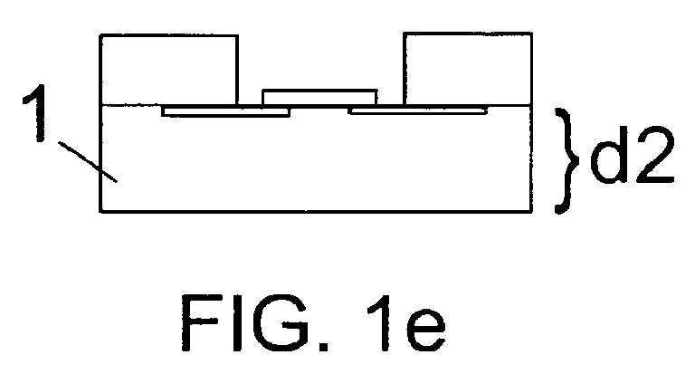
substrate 1, the thickness d1 of thesubstrate 1 may be reduced in order to achieve holes with a diameter smaller than the diameter of holes etched into a substrate / wafer having a standard thickness. - In the step represented by
Figure 1e , thesubstrate 1 is thinned, e.g. by grinding, to a reduced thickness d2 less than 300 µm, preferably less than 100 µm, and in a very preferred embodiment less than 50 µm. This means, that material from thesubstrate 1 is removed for reducing the thickness d1 of thesubstrate 1 down to the reduced thickness d2 in order to allow etching small size/diameter holes for realizing vias, a diameter of which holes depends on the thickness of thesubstrate 1. For example, by using an anisotropic etching technique for building holes reaching through thesubstrate 1 of 150 µm thickness the diameter of such holes may be in the order of 75 um. In case thesubstrate 1 may be thinned down to at least 50 µm, isotropic etching techniques may also be applied instead. As a result,multiple holes 14 forvias 15 can be etched into thesubstrate 1 after thesubstrate 1 has been thinned to the reduced thickness d2 without claiming the entire space on the chip surface. For many sensor applications, at least four through-silicon vias are formed, two for power, and two for communication. - The functionality of the
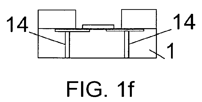
spacer 3 may now be two fold: First, for thinning thesubstrate 1 the present sensor chip may need to be flipped and sit on a support. In such position, with thespacer 3 facing the support thesensing element 2 is protected by thespacer 3 in that thesensing element 2 does not get in touch with the support. And second, thespacer 3 may additionally act as a stiffener to the present sensor chip for the reason that as a result of the thinning step the thickness of thesubstrate 1 may be reduced to levels at which thesubstrate 1 no longer forms a rigid element but rather represents a thin flexible element. In order to compensate for the flexibility achieved as a by-product of the efforts of reducing the diameter of the through vias, thespacer 3 allows the sensor chip to form a rather rigid structure again and improves mechanical stability of the sensor chip and its handling. - A state of the sensor chip after etching holes 14 into the
substrate 1 is shown inFigure 1f . Theholes 14 preferably are etched into thesubstrate 1 from itsback side 12. In a final step, theholes 14 are filled with conducting material such as Cu, polySi, Si, or others for implementing thevarious vias 15. In this context, a via 15 is understood as a conducting element reaching through thesubstrate 1.Conductors 17 provided at theback side 12 of thesubstrate 1 may connect thevias 15 to contactpads 16 provided elsewhere on theback side 12 of thesubstrate 1. In this respect, theback side 12 of thesubstrate 1 may be understood as a redistribution layer which allows for finally arrangingsolder balls 18 on thecontact pads 16 with a sufficient distance from each other, such as shown inFigure 1g . Theconductors 17 of such redistribution layer may be formed on thesubstrate 1 at the very beginning of the process, for example, after the step illustrated inFigure 1b . In another embodiment, where feasible in terms of space, some or all ends of the vias 15 at theback side 12 of thesubstrate 1 may form or especially be formed ascontact pads 16. During etching and filling theholes 14, the sensor chip may be flipped and be seated on itsspacer 3 which again protects thesensing element 2 and the other integrated structures during manufacturing. As a result, no other carrier is needed during building the through-silicon vias 15. - For the present embodiment of a manufacturing process it is advantageous that the material used for the
spacer 3 may show a high temperature stability and may be insensitive to treatments used during building the through-silicon vias 15 for the reason that thespacer 3 may be exposed to high temperatures and such treatments during building the through-silicon vias 15. - In an advantageous embodiment, the
spacer 3 may comprise a membrane being arranged distant from thesensing element 2 for covering theopening 31. An example ofsuch membrane 51 is shown inFigure 2e .Such membrane 51 may be a polymer layer, be bonded to thespacer 3, and be provided as temporary protection during manufacturing, or, alternatively, as a permanent cover provided it allows sufficient access to thesensing element 2. - The sensor chip according to
Figure 1g represents a sensor chip according to an embodiment of the present invention. Such sensor chip can now be mounted to a circuit board with itsback side 11 facing the circuit board. For such mounting, the sensor chip may be pressed with its solder bumps 18 against the circuit board, which in one embodiment may be a printed circuit board, in order to establish an electrical connection between thecontact pads 16 of the sensor chip and contact pads of the circuit board. The solder bumps 18 may be hardened or otherwise treated such that a reliable electrical connection is established. In addition, the sensor chip may be mechanically fixed to the circuit board, for example by means of an adhesive at theback side 12 of the sensor chip, or by other means. - As a result, the
front side 11 of the sensor chip, and in particular itssensing element 2, faces the environment. In such arrangement, the circuit board can be shielded from the measuring environment, for instance by means of an additional housing which may be sealed against thespacer 3. The spacer continues to provide protection to thesensing element 2 also during operation of the sensor chip. At the same time, thesensing element 2 is sufficiently exposed to the measurement environment. There are no elements preventing access to thesensing element 2 as are when the sensor chip would be flip chip mounted to the circuit board. Any sensor signal from the sensing element or signals derived from such sensor signal now can be transmitted to the circuitry on the circuit board via theconnectors 13 and thevias 15. - As such, the
vias 15 represent an electrical connection between thefront side 11 of thesubstrate 1 and itsback side 12 and in particular may help to connectconductors 13 at thefront side 11 of thesubstrate 1 withcontact pads 16 on its back side. Thesensor element 2 may be directly connected to theconductors 13 or via other circuitry. In case thesubstrate 1 is embodied as a silicon substrate, thevias 15 may be named through-silicon vias. - The present order of manufacturing steps is advantageous in view of different aspects: In the first steps according to the
Figures 1a to 1c , standard semiconductor chip manufacturing processes may be applied. As mentioned above, thespacer 3 may be applied as protector during manufacturing of thevias 15. However, thespacer 3 may already perform a protecting function earlier in the process during a possible thinning of thesubstrate 1. In this context, it is beneficial that thespacer 3 is already attached to thesubstrate 1 prior to thinning thesubstrate 1 to its reduced thickness d2. - Still, any manufacturing steps may take a different order than listed in the claims. For example, the
sensing element 2 may be arranged at thesubstrate 1 after thespacer 3 has been arranged at thesubstrate 1 provided that the technology for arranging thesensing element 2 is not prevented by the already arrangedspacer 3. Provided handling allows, thespacer 3 may be arranged at thesubstrate 1 only for processing steps such as testing the sensor chip as will be explained in more detail with respect toFigure 2 . Provided handling allows, thevias 15 may be built first, and the circuitry/conductors 13 and thesensing element 2 may also be formed in a later step. - In another embodiment of manufacturing a sensor chip, the circuitry and the
sensitive element 2 are integrated into thesubstrate 1 at the very beginning according toFigures 1a to 1c . In a next step, the thickness d1 of thesubstrate 1 is reduced, for example by means of thinning itsback side 12 according toFigure 1e , however, without thespacer 3 already being applied. In a next step, the through-silicon vias 15 are built according toFigures 1f and 1g , again without thespacer 3 being applied to thesubstrate 1. After having formed the through-silicon vias 15 in thesubstrate 1, thespacer 3 is arranged according toFigure 1d , and solder bumps 18 are attached to thecontact pads 16 such that a sensor chip according toFigure 1g is produced. Such processing is advantageous if the material used for thespacer 3 may show only low temperature stability and/or sensitivity to treatments used during forming the through-silicon vias 15. However, it may be preferred that during the processing of the through-silicon vias 15 a carrier may be applied for supporting the thinnedsubstrate 1 and protecting it from being damaged. -
FIG. 2a - 2l schematically show different states of sensor chip processing on wafer scale, in a longitudinal cut each, according to an embodiment of the present invention. InFigure 2l a resulting sensor chip arranged on a circuit board is illustrated according to an embodiment of the present invention. - In
Figure 2a , instead of a single substrate from which an individual sensor chip may be built, anentire wafer 4 is provided whichwafer 4 constitutes a substrate for multiple sensor chips to be built from. In the present example, the sensor chips are separated from each other into individual elements at the very end of the manufacturing process, as will be explained later. During the entire processing thewafer 4 forms a common substrate for all the sensor chips to be built. Other than that and except for the omitted thinning step - may it be for the reason that thewafer 4 already is prepared to the required thickness or that thewafer 4 can be used in its original thickness, the initial manufacturing steps are the same as illustrated inFigure 1 . - The
wafer 4 is provided with afront side 11, aback side 12, and a height/depth/vertical extension/thickness d1. A length of thewafer 4 and also its width, of course, exceed the length x1 and the width y1 of theindividual substrate 1 as used according toFigure 1a .Circuitry including conductors 13 and possibly other electronic components are integrated into thewafer 4 by means of CMOS processing, seeFigure 2b , now for multiple sensor chips to be built. In the step illustrated inFigure 2c , an array ofsensing elements 2 is formed on or in thewafer 4. Again,such sensing elements 2 can be built by the same processing steps the circuitry is built from, and, for example,such sensing elements 2 may include polymer layers receptive to humidity in the present example such that the sensor chip represents a humidity sensor for measuring a relative humidity of the environment. - The
sensing elements 2 may alternatively be deposited on thewafer 4 in form of a film covering the entire wafer and be structured to finally form theindividual sensing elements 2 as shown inFigure 2c . - Corresponding to the step shown in
Figure 1d , the spacers are applied to thesubstrate 1 subsequently. Applying/arranging thespacers 3 to/at thewafer 4 may include providingmultiple spacers 3 in form of aplate 5. A shown inFigure 2d ,such plate 5 may be aplate 5 of a dry resist, for example, of other suitable material whereopenings 31 for accessing thesensing elements 2 are already prefabricated, or where subsequent to applying theplate 2 to thefront side 11 of thewafer 4such openings 31 are fabricated. In this context, it may be beneficial that theentire plate 5 has a length and width equivalent to the length and width of thewafer 4. Theplate 5 specifically may be made from one of silicon, silicon and a silicon-oxide coating, silicon and a solderable coating, ceramic, ceramic and a silicon-oxide coating, ceramic and a solderable coating, glass, glass and a silicon-oxide coating, glass and a solderable coating, metal, metal and a solderable coating, and a polymer. Alternatively, applying/arranging thespacers 3 to/at thewafer 4 may include buildingmultiple spacers 3 in form of layers deposited on thewafer 4. Alternatively, applying/arranging thespacers 3 to/at thewafer 4 may include buildingmultiple spacers 3 by moulding or casting material onto thewafer 4. - According to
Figure 2e , amembrane layer 51 is deposited on thespacer plate 5 / thespacers 3, for example by bonding, and forms part of thefinal spacers 3. Themembrane layer 51, which may be embodied as a polymer layer, covers theopenings 31, protects thesensing elements 2, is arranged distant from thesensing elements 2, and provides sufficient access for the medium to be measured. In the step represented byFigure 2f , from theback side 12 of thewafer 4 theholes 14 are etched for all the sensor chips, advantageously by deep reactive-ion etching. For this reason, the wafer arrangement is flipped and sits by means of itsmembrane layer 51 on a support not shown. In the step corresponding toFigure 2g , all theholes 14 are filled with conductive material in order to buildvias 15 reaching through the entire reduced thickness d2 of thewafer 4 in order to connect theconductors 13 of each sensor chip to itscontact pads 16 on theback side 12, again, whichcontact pads 16 may be arranged offset from the associated via 15 as shown inFigure 2g , or may be arranged in a line the associatedvias 15 at thebackside 12 of thewafer 4, or may be arranged in any mix of a contact pads arrangement. - In a subsequent step of processing the sensor chips, the wafer arrangement remains in its flipped state and is seated onto a
chuck 6 with itsmembrane layer 51 facing thechuck 6 for the purpose of testing the sensor chips, seeFigure 2h . In both scenarios, electrical connections are established to thecontact pads 16 now being easily accessible. Aprobe head 7 comprisingelectrodes 71 is arranged on top of theback side 12 of thewafer 4 and theelectrodes 71 are brought into contact with thecontact pads 16. Now, test routines may be executed, wherein thesensing elements 2 are protected by the spacers which avoid thesensing elements 2 being in direct contact with thechuck 6. - Advantageously, during test the wafer arrangement may be exposed to a medium evoking sensor responses that can be measured by means of the
electrodes 71. For example, in case the sensor chips are implemented as humidity sensors, then, humid air may be supplied to thesensing elements 2 on thewafer 4. In the arrangement according toFigure 2h such medium advantageously is guided through openings in the chuck 6 - which are not explicitly shown inFigure 2h - for accessing thesensing elements 2 facing thechuck 6. - According to
Figure 2i , thewafer 4 may be cut, for example along the dotted line, in order to separate the sensor chips from each other. The resulting individual sensor chips may be arranged on afoil 8, and possibly glued thereto for transporting purposes only. Prior to separating the individual sensor chips, solder bumps may be applied to some or all thecontact pads 16 on theback side 12 of thewafer 4 in order to prepare a mounting of the individual sensor chips to their destinations such as circuit boards. -
Such foil 8 with multiple sensor chips thereon may be supplied to anautomatic assembly 9 as schematically illustrated inFigure 2l . Apicker 91 picks an individual sensor chip at itsspacer 3 and places such sensor chip onto its final destination which in the present example is acircuit board 10. During the assembly / packaging process, thesensing element 2 as well as the entire sensor chip is protected by means of thespacer 3 which acts as a preferred contact surface for thepicker 91. - Accordingly, the sensor chip is mounted with its back side onto the
circuit board 10 whereas its front side including thesensing element 2 and thespacer 3 are directed away from thecircuit board 10. - Any aspect with respect to the order of manufacturing steps explained in connection with an individual sensor chip according to
Figure 1 holds for the wafer level manufacturing according toFigure 2 , too. Any such variants introduced before may be introduced with respect to the wafer level manufacturing, too. In other variants, after each of the manufacturing steps on the wafer level, it may be switched to subsequent manufacturing on the individual sensor chip level by cutting thewafer 4 and any other overlapping structures. - In preferred embodiments, the sensor chip is used as one of a humidity sensor, a liquid flow sensor, a gas flow sensor, a pressure sensor, an infrared sensor and a chemical sensor. Corresponding sensing elements are provided for each of the applications.
Claims (16)
- Sensor chip, comprising
a substrate (1) with a front side (11) and a back side (12),
a sensing element (2) and conductors (13) arranged at the front side (11),
contact pads (16) arranged at the back side (12),
vias (15) extending through the substrate (1) between the front side (11) and the back side (12) for electrically connecting the conductors (13) to the contact pads (16), and
a spacer (3) arranged at the front side (11) for protecting the sensing element (2). - Sensor chip according to claim 1, wherein the spacer (3) is made of one of a resist, a cast, semiconductor, ceramic, metal, dielectric material, glass.
- Sensor chip according to claim 1 or claim 2, wherein the spacer (3) extends around the sensing element (2).
- Sensor chip according to any one of the preceding claims, wherein the spacer (3) comprises a membrane covering an opening (31) in the spacer (3) for granting access to the sensing element (2) which membrane is disposed at a distance from the sensing element (2).
- Sensor chip according to any one of the preceding claims, wherein a thickness (h1) of the spacer (3) is more than 100 µm, and preferably is between 150 and 250 µm.
- Sensor chip according to any one of the preceding claims, comprising circuitry arranged at the front side (11) of the substrate (1) at least a part of which circuitry is covered by the spacer (3).
- Use of a sensor chip according to any one of the preceding claims as one of a humidity sensor, a liquid flow sensor, a gas flow sensor, a pressure sensor, an infrared sensor and a chemical sensor.
- Method for manufacturing a sensor chip, comprising the steps of
providing a substrate (1) with a front side (11) and a back side (12),
arranging a sensing element (2) at the front side (11),
arranging a spacer (3) at the front side (11),
etching holes (14) into the substrate (1),
and
filling the holes (14) with a conducting material for building vias (15) extending through the substrate (1) between the front side (11) and the back side (12). - Method according to claim 8, wherein the holes (14) are etched by anisotropic etching from the backside (12) of the substrate (1).
- Method according to claim 8 or claim 9,
wherein the sensor chip is arranged on a chuck (6) with the spacer (3) facing the chuck (6) for electrically contacting contact pads (16) arranged at the back side (12) with electrodes (71). - Method according to claim 10, wherein the sensor chip is tested while being arranged on the chuck (6).
- Method according to any one of the preceding claims 8 to 11, wherein a picker (91) of an automatic assembly (9) engages with the spacer (3) of the sensor chip for placing the sensor chip on a circuit board (10).
- Method according to any one of the preceding claims 8 to 12, wherein the spacer (3) is arranged at the front side (11) after the vias(15) are built.
- Method according to any one of the preceding claims 8 to 12, wherein the spacer (3) is arranged at the front side (11) prior to etching the holes (14).
- Method according to any one of the preceding claims 8 to 14,
wherein the substrate (1) is provided in form of a wafer (4) for building multiple sensor chips from, and
wherein sensing elements (2) and conductors (13) for multiple sensor chips are arranged at the front side (11) of the wafer (4),
wherein multiple spacers (3) for multiple sensor chips are arranged at the front side (11) of the wafer (4),
wherein the step of etching holes (14) through the wafer (4) and filling the holes (14) for building vias (15) for multiple sensor chips is applied prior to or after the spacers (3) are arranged at the wafer (4), and
wherein the previous four steps are implemented prior to separating the wafer (4) into multiple sensor chips. - Method according to claim 15, wherein a membrane layer (51) is applied onto the spacers (3).
Priority Applications (9)
| Application Number | Priority Date | Filing Date | Title |
|---|---|---|---|
| EP11000640.0A EP2481703B1 (en) | 2011-01-27 | 2011-01-27 | Sensor protection |
| EP12702167.3A EP2668130A1 (en) | 2011-01-27 | 2012-01-26 | Sensor chip comprising a spacer for protecting the sensor element |
| PCT/CH2012/000020 WO2012100361A2 (en) | 2011-01-27 | 2012-01-26 | Sensor protection |
| US13/981,651 US9366720B2 (en) | 2011-01-27 | 2012-01-26 | Sensor protection |
| JP2013550722A JP6038048B2 (en) | 2011-01-27 | 2012-01-26 | Method of manufacturing sensor chip having apparatus for testing sensor chip |
| EP12702168.1A EP2668131A2 (en) | 2011-01-27 | 2012-01-26 | Method for manufacturing a sensor chip comprising a device for testing it |
| KR1020137022245A KR101944128B1 (en) | 2011-01-27 | 2012-01-26 | Method for manufacturing a sensor chip comprising a device for testing it |
| PCT/CH2012/000021 WO2012100362A1 (en) | 2011-01-27 | 2012-01-26 | Method for manufacturing a sensor chip |
| PCT/CH2012/000019 WO2012100360A1 (en) | 2011-01-27 | 2012-01-26 | Sensor chip comprising a spacer for protecting the sensor element |
Applications Claiming Priority (1)
| Application Number | Priority Date | Filing Date | Title |
|---|---|---|---|
| EP11000640.0A EP2481703B1 (en) | 2011-01-27 | 2011-01-27 | Sensor protection |
Publications (2)
| Publication Number | Publication Date |
|---|---|
| EP2481703A1 true EP2481703A1 (en) | 2012-08-01 |
| EP2481703B1 EP2481703B1 (en) | 2020-07-01 |
Family
ID=44148336
Family Applications (3)
| Application Number | Title | Priority Date | Filing Date |
|---|---|---|---|
| EP11000640.0A Active EP2481703B1 (en) | 2011-01-27 | 2011-01-27 | Sensor protection |
| EP12702168.1A Withdrawn EP2668131A2 (en) | 2011-01-27 | 2012-01-26 | Method for manufacturing a sensor chip comprising a device for testing it |
| EP12702167.3A Withdrawn EP2668130A1 (en) | 2011-01-27 | 2012-01-26 | Sensor chip comprising a spacer for protecting the sensor element |
Family Applications After (2)
| Application Number | Title | Priority Date | Filing Date |
|---|---|---|---|
| EP12702168.1A Withdrawn EP2668131A2 (en) | 2011-01-27 | 2012-01-26 | Method for manufacturing a sensor chip comprising a device for testing it |
| EP12702167.3A Withdrawn EP2668130A1 (en) | 2011-01-27 | 2012-01-26 | Sensor chip comprising a spacer for protecting the sensor element |
Country Status (5)
| Country | Link |
|---|---|
| US (1) | US9366720B2 (en) |
| EP (3) | EP2481703B1 (en) |
| JP (1) | JP6038048B2 (en) |
| KR (1) | KR101944128B1 (en) |
| WO (3) | WO2012100360A1 (en) |
Cited By (4)
| Publication number | Priority date | Publication date | Assignee | Title |
|---|---|---|---|---|
| EP2762870A1 (en) * | 2013-01-31 | 2014-08-06 | Sensirion AG | Sensor arrangement and portable electronic device with such a sensor arrangement |
| EP2871152A1 (en) | 2013-11-06 | 2015-05-13 | Sensirion AG | Sensor device |
| EP2917935A1 (en) * | 2012-11-07 | 2015-09-16 | Ams Ag | Semiconductor sensor device and method of producing a semiconductor sensor device |
| EP3001186A1 (en) * | 2014-09-26 | 2016-03-30 | Sensirion AG | Sensor chip |
Families Citing this family (20)
| Publication number | Priority date | Publication date | Assignee | Title |
|---|---|---|---|---|
| EP2762869B1 (en) | 2013-01-31 | 2016-11-16 | Sensirion AG | Integrated metal oxide chemical sensor |
| EP2763381B1 (en) | 2013-01-31 | 2017-04-05 | Sensirion AG | Portable electronic device with chemical sensor |
| EP2762880B1 (en) | 2013-01-31 | 2017-03-15 | Sensirion AG | Portable electronic device with breath analyzer |
| EP2762865A1 (en) * | 2013-01-31 | 2014-08-06 | Sensirion Holding AG | Chemical sensor and method for manufacturing such a chemical sensor |
| EP2762882B1 (en) | 2013-01-31 | 2020-11-25 | Sensirion AG | Portable electronic device with ketone sensor |
| EP2801819A1 (en) | 2013-05-08 | 2014-11-12 | Sensirion AG | Metal oxide chemical sensor for portable device |
| EP2808675A1 (en) | 2013-05-31 | 2014-12-03 | Sensirion AG | Integrated metal oxide chemical sensor |
| DE202013102632U1 (en) * | 2013-06-19 | 2013-12-20 | Sensirion Ag | sensor module |
| EP2816352B1 (en) | 2013-06-21 | 2016-12-28 | Sensirion AG | Concentration measurements with a mobile device |
| EP2833128A1 (en) | 2013-07-30 | 2015-02-04 | Sensirion AG | Integrated metal oxide chemical sensor |
| EP2833127A1 (en) | 2013-07-30 | 2015-02-04 | Sensirion AG | Integrated resistive-type sensor array arrangement, each sensor comprising a sensitive metal oxide layer each having a different length between the electrodes |
| EP2946722A1 (en) | 2014-05-20 | 2015-11-25 | Sensirion AG | Portable electronic device for breath sampling |
| WO2016088099A1 (en) * | 2014-12-05 | 2016-06-09 | Lfoundry S.R.L. | Cmos process for manufacturing an integrated gas sensor and corresponding cmos integrated gas sensor |
| EP3032227B1 (en) | 2014-12-08 | 2020-10-21 | Sensirion AG | Flow sensor package |
| WO2016204525A1 (en) * | 2015-06-19 | 2016-12-22 | 엘지전자(주) | Touch panel and display device |
| GB2568633B (en) | 2016-09-21 | 2022-06-29 | Sensirion Ag | Gas sensor |
| JP6917843B2 (en) * | 2016-10-13 | 2021-08-11 | 理研計器株式会社 | Gas sensor |
| US20180196022A1 (en) * | 2017-01-12 | 2018-07-12 | Integrated Device Technology, Inc. | Gas sensor |
| KR20190035989A (en) | 2017-09-25 | 2019-04-04 | (주)센텍코리아 | Gas sensor package |
| US10727216B1 (en) | 2019-05-10 | 2020-07-28 | Sandisk Technologies Llc | Method for removing a bulk substrate from a bonded assembly of wafers |
Citations (7)
| Publication number | Priority date | Publication date | Assignee | Title |
|---|---|---|---|---|
| WO2001056920A2 (en) * | 2000-02-01 | 2001-08-09 | Motorola, Inc. | Micro-electromechanical system device |
| US6528875B1 (en) * | 2001-04-20 | 2003-03-04 | Amkor Technology, Inc. | Vacuum sealed package for semiconductor chip |
| US20050104204A1 (en) * | 2003-09-30 | 2005-05-19 | Takashi Kawakubo | Wafer-level package and its manufacturing method |
| WO2005102911A1 (en) * | 2004-04-19 | 2005-11-03 | Analog Devices, Inc. | Mems device with conductive path through substrate |
| US20060179942A1 (en) * | 2005-02-16 | 2006-08-17 | Mitsubishi Denki Kabushiki Kaisha | Acceleration sensor |
| US20080283991A1 (en) * | 2007-05-14 | 2008-11-20 | Fraunhofer-Gesellschaft Zur Foerderung Der Angewandten Forschung E.V. | Housed active microstructures with direct contacting to a substrate |
| US20080315230A1 (en) * | 2007-06-20 | 2008-12-25 | Shinko Electric Industries Co., Ltd. | Electronic component package and method of manufacturing the same, and electronic component device |
Family Cites Families (28)
| Publication number | Priority date | Publication date | Assignee | Title |
|---|---|---|---|---|
| EP0265816B1 (en) | 1986-10-28 | 1991-08-28 | Sumitomo Electric Industries Limited | Method of measuring semiconductor pressure sensor |
| JPS63110671A (en) | 1986-10-28 | 1988-05-16 | Sumitomo Electric Ind Ltd | Measurement method of semiconductor pressure sensor |
| JPH0233567A (en) | 1988-07-20 | 1990-02-02 | Matsushita Electric Ind Co Ltd | Hot air heater |
| US5001423A (en) | 1990-01-24 | 1991-03-19 | International Business Machines Corporation | Dry interface thermal chuck temperature control system for semiconductor wafer testing |
| DE4239132C2 (en) * | 1991-11-20 | 2002-06-06 | Denso Corp | Method of fabricating an integrated pressure sensor |
| JPH0933567A (en) * | 1995-07-21 | 1997-02-07 | Akebono Brake Ind Co Ltd | Method and device for inspecting sensor chip of semiconductor acceleration sensor |
| US5865938A (en) | 1996-06-25 | 1999-02-02 | Xerox Corporation | Wafer chuck for inducing an electrical bias across wafer heterojunctions |
| US6083344A (en) * | 1997-05-29 | 2000-07-04 | Applied Materials, Inc. | Multi-zone RF inductively coupled source configuration |
| US6189483B1 (en) * | 1997-05-29 | 2001-02-20 | Applied Materials, Inc. | Process kit |
| EP1236038B1 (en) | 1999-12-08 | 2005-11-23 | Sensirion AG | Capacitive sensor |
| WO2001055702A1 (en) * | 2000-01-31 | 2001-08-02 | Board Of Regents, The University Of Texas System | Portable sensor array system |
| US6479320B1 (en) | 2000-02-02 | 2002-11-12 | Raytheon Company | Vacuum package fabrication of microelectromechanical system devices with integrated circuit components |
| US6624003B1 (en) * | 2002-02-06 | 2003-09-23 | Teravicta Technologies, Inc. | Integrated MEMS device and package |
| US20050029221A1 (en) * | 2003-08-09 | 2005-02-10 | Taiwan Semiconductor Manufacturing Co., Ltd. | Deep trench etching using HDP chamber |
| DE102004003413A1 (en) * | 2004-01-23 | 2005-08-11 | Robert Bosch Gmbh | Method for packaging semiconductor chips and corresponding semiconductor chip arrangement |
| EP1628132B1 (en) | 2004-08-17 | 2015-01-07 | Sensirion Holding AG | Method and device for calibrating sensors |
| JP2006173557A (en) | 2004-11-22 | 2006-06-29 | Toshiba Corp | Hollow semiconductor device and manufacturing method thereof |
| DE102005014427B4 (en) * | 2005-03-24 | 2008-05-15 | Infineon Technologies Ag | Method for encapsulating a semiconductor device |
| JP4889974B2 (en) * | 2005-08-01 | 2012-03-07 | 新光電気工業株式会社 | Electronic component mounting structure and manufacturing method thereof |
| US20070190747A1 (en) * | 2006-01-23 | 2007-08-16 | Tessera Technologies Hungary Kft. | Wafer level packaging to lidded chips |
| US7936062B2 (en) * | 2006-01-23 | 2011-05-03 | Tessera Technologies Ireland Limited | Wafer level chip packaging |
| JP5270349B2 (en) * | 2006-08-25 | 2013-08-21 | セミコンダクター・コンポーネンツ・インダストリーズ・リミテッド・ライアビリティ・カンパニー | Semiconductor device and manufacturing method thereof |
| US8390117B2 (en) * | 2007-12-11 | 2013-03-05 | Panasonic Corporation | Semiconductor device and method of manufacturing the same |
| US20090178751A1 (en) * | 2007-12-11 | 2009-07-16 | Micro Foundry Inc. | Integrated miniature microfluidics device factory and method for use |
| JP5247396B2 (en) * | 2008-07-02 | 2013-07-24 | 日本化薬株式会社 | Photosensitive resin composition for MEMS and cured product thereof |
| EP2154713B1 (en) * | 2008-08-11 | 2013-01-02 | Sensirion AG | Method for manufacturing a sensor device with a stress relief layer |
| JP5535492B2 (en) * | 2009-02-12 | 2014-07-02 | ラピスセミコンダクタ株式会社 | Semiconductor integrated circuit inspection apparatus and semiconductor integrated circuit inspection method |
| EP2252077B1 (en) | 2009-05-11 | 2012-07-11 | STMicroelectronics Srl | Assembly of a capacitive acoustic transducer of the microelectromechanical type and package thereof |
-
2011
- 2011-01-27 EP EP11000640.0A patent/EP2481703B1/en active Active
-
2012
- 2012-01-26 JP JP2013550722A patent/JP6038048B2/en active Active
- 2012-01-26 WO PCT/CH2012/000019 patent/WO2012100360A1/en not_active Ceased
- 2012-01-26 WO PCT/CH2012/000021 patent/WO2012100362A1/en not_active Ceased
- 2012-01-26 EP EP12702168.1A patent/EP2668131A2/en not_active Withdrawn
- 2012-01-26 KR KR1020137022245A patent/KR101944128B1/en active Active
- 2012-01-26 EP EP12702167.3A patent/EP2668130A1/en not_active Withdrawn
- 2012-01-26 WO PCT/CH2012/000020 patent/WO2012100361A2/en not_active Ceased
- 2012-01-26 US US13/981,651 patent/US9366720B2/en active Active
Patent Citations (7)
| Publication number | Priority date | Publication date | Assignee | Title |
|---|---|---|---|---|
| WO2001056920A2 (en) * | 2000-02-01 | 2001-08-09 | Motorola, Inc. | Micro-electromechanical system device |
| US6528875B1 (en) * | 2001-04-20 | 2003-03-04 | Amkor Technology, Inc. | Vacuum sealed package for semiconductor chip |
| US20050104204A1 (en) * | 2003-09-30 | 2005-05-19 | Takashi Kawakubo | Wafer-level package and its manufacturing method |
| WO2005102911A1 (en) * | 2004-04-19 | 2005-11-03 | Analog Devices, Inc. | Mems device with conductive path through substrate |
| US20060179942A1 (en) * | 2005-02-16 | 2006-08-17 | Mitsubishi Denki Kabushiki Kaisha | Acceleration sensor |
| US20080283991A1 (en) * | 2007-05-14 | 2008-11-20 | Fraunhofer-Gesellschaft Zur Foerderung Der Angewandten Forschung E.V. | Housed active microstructures with direct contacting to a substrate |
| US20080315230A1 (en) * | 2007-06-20 | 2008-12-25 | Shinko Electric Industries Co., Ltd. | Electronic component package and method of manufacturing the same, and electronic component device |
Cited By (9)
| Publication number | Priority date | Publication date | Assignee | Title |
|---|---|---|---|---|
| EP2917935A1 (en) * | 2012-11-07 | 2015-09-16 | Ams Ag | Semiconductor sensor device and method of producing a semiconductor sensor device |
| EP2762870A1 (en) * | 2013-01-31 | 2014-08-06 | Sensirion AG | Sensor arrangement and portable electronic device with such a sensor arrangement |
| EP2871152A1 (en) | 2013-11-06 | 2015-05-13 | Sensirion AG | Sensor device |
| US10281442B2 (en) | 2013-11-06 | 2019-05-07 | Sensirion Ag | Sensor device |
| EP3001186A1 (en) * | 2014-09-26 | 2016-03-30 | Sensirion AG | Sensor chip |
| KR20160037119A (en) * | 2014-09-26 | 2016-04-05 | 센시리온 에이지 | Sensor chip |
| CN105466463A (en) * | 2014-09-26 | 2016-04-06 | 盛思锐股份公司 | sensor chip |
| US9506885B2 (en) | 2014-09-26 | 2016-11-29 | Sensirion Ag | Sensor chip |
| CN105466463B (en) * | 2014-09-26 | 2019-11-15 | 盛思锐股份公司 | sensor chip |
Also Published As
| Publication number | Publication date |
|---|---|
| EP2668130A1 (en) | 2013-12-04 |
| WO2012100360A1 (en) | 2012-08-02 |
| JP2014508288A (en) | 2014-04-03 |
| KR101944128B1 (en) | 2019-01-30 |
| US20140028340A1 (en) | 2014-01-30 |
| WO2012100362A1 (en) | 2012-08-02 |
| WO2012100361A3 (en) | 2012-11-15 |
| EP2481703B1 (en) | 2020-07-01 |
| WO2012100361A2 (en) | 2012-08-02 |
| US9366720B2 (en) | 2016-06-14 |
| KR20140006908A (en) | 2014-01-16 |
| EP2668131A2 (en) | 2013-12-04 |
| JP6038048B2 (en) | 2016-12-07 |
Similar Documents
| Publication | Publication Date | Title |
|---|---|---|
| EP2481703A1 (en) | Sensor protection | |
| EP2755023B1 (en) | Capacitive sensor integrated onto semiconductor circuit | |
| TWI685464B (en) | Pressure sensor and manufacturing method thereof | |
| EP3001186B1 (en) | Sensor chip | |
| US10161817B2 (en) | Reduced stress pressure sensor | |
| CN104773705A (en) | Micromechanical pressure sensor device and corresponding manufacturing method | |
| TW201400401A (en) | Hybrid integrated component and method of manufacturing same | |
| EP2482310B1 (en) | Through vias in a sensor chip | |
| TW201350424A (en) | Method of manufacturing a hybrid integrated component | |
| EP3601957B1 (en) | Sensor package | |
| US20170057810A1 (en) | Strain Reduction and Sensing on Package Substrates | |
| US11366031B2 (en) | Semiconductor device and method for forming a semiconductor device | |
| CN116281835B (en) | MEMS device, preparation method thereof and electronic device | |
| US20170284881A1 (en) | Electronic part | |
| JP2004317339A (en) | Capacitance type external force detection device | |
| JP2010151631A (en) | Acceleration sensor element, acceleration sensor device, and method of manufacturing the acceleration sensor element |
Legal Events
| Date | Code | Title | Description |
|---|---|---|---|
| PUAI | Public reference made under article 153(3) epc to a published international application that has entered the european phase |
Free format text: ORIGINAL CODE: 0009012 |
|
| AK | Designated contracting states |
Kind code of ref document: A1 Designated state(s): AL AT BE BG CH CY CZ DE DK EE ES FI FR GB GR HR HU IE IS IT LI LT LU LV MC MK MT NL NO PL PT RO RS SE SI SK SM TR |
|
| AX | Request for extension of the european patent |
Extension state: BA ME |
|
| 17P | Request for examination filed |
Effective date: 20130201 |
|
| 17Q | First examination report despatched |
Effective date: 20140905 |
|
| STAA | Information on the status of an ep patent application or granted ep patent |
Free format text: STATUS: EXAMINATION IS IN PROGRESS |
|
| GRAP | Despatch of communication of intention to grant a patent |
Free format text: ORIGINAL CODE: EPIDOSNIGR1 |
|
| STAA | Information on the status of an ep patent application or granted ep patent |
Free format text: STATUS: GRANT OF PATENT IS INTENDED |
|
| INTG | Intention to grant announced |
Effective date: 20200218 |
|
| GRAS | Grant fee paid |
Free format text: ORIGINAL CODE: EPIDOSNIGR3 |
|
| GRAA | (expected) grant |
Free format text: ORIGINAL CODE: 0009210 |
|
| STAA | Information on the status of an ep patent application or granted ep patent |
Free format text: STATUS: THE PATENT HAS BEEN GRANTED |
|
| AK | Designated contracting states |
Kind code of ref document: B1 Designated state(s): AL AT BE BG CH CY CZ DE DK EE ES FI FR GB GR HR HU IE IS IT LI LT LU LV MC MK MT NL NO PL PT RO RS SE SI SK SM TR |
|
| REG | Reference to a national code |
Ref country code: GB Ref legal event code: FG4D |
|
| REG | Reference to a national code |
Ref country code: AT Ref legal event code: REF Ref document number: 1286024 Country of ref document: AT Kind code of ref document: T Effective date: 20200715 Ref country code: CH Ref legal event code: EP |
|
| REG | Reference to a national code |
Ref country code: IE Ref legal event code: FG4D |
|
| REG | Reference to a national code |
Ref country code: DE Ref legal event code: R096 Ref document number: 602011067533 Country of ref document: DE |
|
| REG | Reference to a national code |
Ref country code: LT Ref legal event code: MG4D |
|
| PG25 | Lapsed in a contracting state [announced via postgrant information from national office to epo] |
Ref country code: BG Free format text: LAPSE BECAUSE OF FAILURE TO SUBMIT A TRANSLATION OF THE DESCRIPTION OR TO PAY THE FEE WITHIN THE PRESCRIBED TIME-LIMIT Effective date: 20201001 |
|
| REG | Reference to a national code |
Ref country code: NL Ref legal event code: MP Effective date: 20200701 |
|
| REG | Reference to a national code |
Ref country code: AT Ref legal event code: MK05 Ref document number: 1286024 Country of ref document: AT Kind code of ref document: T Effective date: 20200701 |
|
| PG25 | Lapsed in a contracting state [announced via postgrant information from national office to epo] |
Ref country code: HR Free format text: LAPSE BECAUSE OF FAILURE TO SUBMIT A TRANSLATION OF THE DESCRIPTION OR TO PAY THE FEE WITHIN THE PRESCRIBED TIME-LIMIT Effective date: 20200701 Ref country code: ES Free format text: LAPSE BECAUSE OF FAILURE TO SUBMIT A TRANSLATION OF THE DESCRIPTION OR TO PAY THE FEE WITHIN THE PRESCRIBED TIME-LIMIT Effective date: 20200701 Ref country code: SE Free format text: LAPSE BECAUSE OF FAILURE TO SUBMIT A TRANSLATION OF THE DESCRIPTION OR TO PAY THE FEE WITHIN THE PRESCRIBED TIME-LIMIT Effective date: 20200701 Ref country code: NO Free format text: LAPSE BECAUSE OF FAILURE TO SUBMIT A TRANSLATION OF THE DESCRIPTION OR TO PAY THE FEE WITHIN THE PRESCRIBED TIME-LIMIT Effective date: 20201001 Ref country code: GR Free format text: LAPSE BECAUSE OF FAILURE TO SUBMIT A TRANSLATION OF THE DESCRIPTION OR TO PAY THE FEE WITHIN THE PRESCRIBED TIME-LIMIT Effective date: 20201002 Ref country code: AT Free format text: LAPSE BECAUSE OF FAILURE TO SUBMIT A TRANSLATION OF THE DESCRIPTION OR TO PAY THE FEE WITHIN THE PRESCRIBED TIME-LIMIT Effective date: 20200701 Ref country code: PT Free format text: LAPSE BECAUSE OF FAILURE TO SUBMIT A TRANSLATION OF THE DESCRIPTION OR TO PAY THE FEE WITHIN THE PRESCRIBED TIME-LIMIT Effective date: 20201102 Ref country code: LT Free format text: LAPSE BECAUSE OF FAILURE TO SUBMIT A TRANSLATION OF THE DESCRIPTION OR TO PAY THE FEE WITHIN THE PRESCRIBED TIME-LIMIT Effective date: 20200701 Ref country code: FI Free format text: LAPSE BECAUSE OF FAILURE TO SUBMIT A TRANSLATION OF THE DESCRIPTION OR TO PAY THE FEE WITHIN THE PRESCRIBED TIME-LIMIT Effective date: 20200701 Ref country code: CZ Free format text: LAPSE BECAUSE OF FAILURE TO SUBMIT A TRANSLATION OF THE DESCRIPTION OR TO PAY THE FEE WITHIN THE PRESCRIBED TIME-LIMIT Effective date: 20200701 |
|
| PG25 | Lapsed in a contracting state [announced via postgrant information from national office to epo] |
Ref country code: IS Free format text: LAPSE BECAUSE OF FAILURE TO SUBMIT A TRANSLATION OF THE DESCRIPTION OR TO PAY THE FEE WITHIN THE PRESCRIBED TIME-LIMIT Effective date: 20201101 Ref country code: LV Free format text: LAPSE BECAUSE OF FAILURE TO SUBMIT A TRANSLATION OF THE DESCRIPTION OR TO PAY THE FEE WITHIN THE PRESCRIBED TIME-LIMIT Effective date: 20200701 Ref country code: RS Free format text: LAPSE BECAUSE OF FAILURE TO SUBMIT A TRANSLATION OF THE DESCRIPTION OR TO PAY THE FEE WITHIN THE PRESCRIBED TIME-LIMIT Effective date: 20200701 Ref country code: PL Free format text: LAPSE BECAUSE OF FAILURE TO SUBMIT A TRANSLATION OF THE DESCRIPTION OR TO PAY THE FEE WITHIN THE PRESCRIBED TIME-LIMIT Effective date: 20200701 |
|
| PG25 | Lapsed in a contracting state [announced via postgrant information from national office to epo] |
Ref country code: NL Free format text: LAPSE BECAUSE OF FAILURE TO SUBMIT A TRANSLATION OF THE DESCRIPTION OR TO PAY THE FEE WITHIN THE PRESCRIBED TIME-LIMIT Effective date: 20200701 |
|
| REG | Reference to a national code |
Ref country code: DE Ref legal event code: R097 Ref document number: 602011067533 Country of ref document: DE |
|
| PG25 | Lapsed in a contracting state [announced via postgrant information from national office to epo] |
Ref country code: SM Free format text: LAPSE BECAUSE OF FAILURE TO SUBMIT A TRANSLATION OF THE DESCRIPTION OR TO PAY THE FEE WITHIN THE PRESCRIBED TIME-LIMIT Effective date: 20200701 Ref country code: RO Free format text: LAPSE BECAUSE OF FAILURE TO SUBMIT A TRANSLATION OF THE DESCRIPTION OR TO PAY THE FEE WITHIN THE PRESCRIBED TIME-LIMIT Effective date: 20200701 Ref country code: IT Free format text: LAPSE BECAUSE OF FAILURE TO SUBMIT A TRANSLATION OF THE DESCRIPTION OR TO PAY THE FEE WITHIN THE PRESCRIBED TIME-LIMIT Effective date: 20200701 Ref country code: EE Free format text: LAPSE BECAUSE OF FAILURE TO SUBMIT A TRANSLATION OF THE DESCRIPTION OR TO PAY THE FEE WITHIN THE PRESCRIBED TIME-LIMIT Effective date: 20200701 Ref country code: DK Free format text: LAPSE BECAUSE OF FAILURE TO SUBMIT A TRANSLATION OF THE DESCRIPTION OR TO PAY THE FEE WITHIN THE PRESCRIBED TIME-LIMIT Effective date: 20200701 |
|
| PLBE | No opposition filed within time limit |
Free format text: ORIGINAL CODE: 0009261 |
|
| STAA | Information on the status of an ep patent application or granted ep patent |
Free format text: STATUS: NO OPPOSITION FILED WITHIN TIME LIMIT |
|
| PG25 | Lapsed in a contracting state [announced via postgrant information from national office to epo] |
Ref country code: AL Free format text: LAPSE BECAUSE OF FAILURE TO SUBMIT A TRANSLATION OF THE DESCRIPTION OR TO PAY THE FEE WITHIN THE PRESCRIBED TIME-LIMIT Effective date: 20200701 |
|
| 26N | No opposition filed |
Effective date: 20210406 |
|
| PG25 | Lapsed in a contracting state [announced via postgrant information from national office to epo] |
Ref country code: SK Free format text: LAPSE BECAUSE OF FAILURE TO SUBMIT A TRANSLATION OF THE DESCRIPTION OR TO PAY THE FEE WITHIN THE PRESCRIBED TIME-LIMIT Effective date: 20200701 |
|
| PG25 | Lapsed in a contracting state [announced via postgrant information from national office to epo] |
Ref country code: MC Free format text: LAPSE BECAUSE OF FAILURE TO SUBMIT A TRANSLATION OF THE DESCRIPTION OR TO PAY THE FEE WITHIN THE PRESCRIBED TIME-LIMIT Effective date: 20200701 Ref country code: SI Free format text: LAPSE BECAUSE OF FAILURE TO SUBMIT A TRANSLATION OF THE DESCRIPTION OR TO PAY THE FEE WITHIN THE PRESCRIBED TIME-LIMIT Effective date: 20200701 |
|
| GBPC | Gb: european patent ceased through non-payment of renewal fee |
Effective date: 20210127 |
|
| PG25 | Lapsed in a contracting state [announced via postgrant information from national office to epo] |
Ref country code: LU Free format text: LAPSE BECAUSE OF NON-PAYMENT OF DUE FEES Effective date: 20210127 |
|
| REG | Reference to a national code |
Ref country code: BE Ref legal event code: MM Effective date: 20210131 |
|
| PG25 | Lapsed in a contracting state [announced via postgrant information from national office to epo] |
Ref country code: FR Free format text: LAPSE BECAUSE OF NON-PAYMENT OF DUE FEES Effective date: 20210131 |
|
| PG25 | Lapsed in a contracting state [announced via postgrant information from national office to epo] |
Ref country code: GB Free format text: LAPSE BECAUSE OF NON-PAYMENT OF DUE FEES Effective date: 20210127 |
|
| PG25 | Lapsed in a contracting state [announced via postgrant information from national office to epo] |
Ref country code: IE Free format text: LAPSE BECAUSE OF NON-PAYMENT OF DUE FEES Effective date: 20210127 |
|
| PG25 | Lapsed in a contracting state [announced via postgrant information from national office to epo] |
Ref country code: IS Free format text: LAPSE BECAUSE OF FAILURE TO SUBMIT A TRANSLATION OF THE DESCRIPTION OR TO PAY THE FEE WITHIN THE PRESCRIBED TIME-LIMIT Effective date: 20201101 |
|
| PG25 | Lapsed in a contracting state [announced via postgrant information from national office to epo] |
Ref country code: BE Free format text: LAPSE BECAUSE OF NON-PAYMENT OF DUE FEES Effective date: 20210131 |
|
| PG25 | Lapsed in a contracting state [announced via postgrant information from national office to epo] |
Ref country code: HU Free format text: LAPSE BECAUSE OF FAILURE TO SUBMIT A TRANSLATION OF THE DESCRIPTION OR TO PAY THE FEE WITHIN THE PRESCRIBED TIME-LIMIT; INVALID AB INITIO Effective date: 20110127 Ref country code: CY Free format text: LAPSE BECAUSE OF FAILURE TO SUBMIT A TRANSLATION OF THE DESCRIPTION OR TO PAY THE FEE WITHIN THE PRESCRIBED TIME-LIMIT Effective date: 20200701 |
|
| P01 | Opt-out of the competence of the unified patent court (upc) registered |
Effective date: 20230602 |
|
| PG25 | Lapsed in a contracting state [announced via postgrant information from national office to epo] |
Ref country code: MK Free format text: LAPSE BECAUSE OF FAILURE TO SUBMIT A TRANSLATION OF THE DESCRIPTION OR TO PAY THE FEE WITHIN THE PRESCRIBED TIME-LIMIT Effective date: 20200701 |
|
| PG25 | Lapsed in a contracting state [announced via postgrant information from national office to epo] |
Ref country code: TR Free format text: LAPSE BECAUSE OF FAILURE TO SUBMIT A TRANSLATION OF THE DESCRIPTION OR TO PAY THE FEE WITHIN THE PRESCRIBED TIME-LIMIT Effective date: 20200701 |
|
| PG25 | Lapsed in a contracting state [announced via postgrant information from national office to epo] |
Ref country code: MT Free format text: LAPSE BECAUSE OF FAILURE TO SUBMIT A TRANSLATION OF THE DESCRIPTION OR TO PAY THE FEE WITHIN THE PRESCRIBED TIME-LIMIT Effective date: 20200701 |
|
| PGFP | Annual fee paid to national office [announced via postgrant information from national office to epo] |
Ref country code: DE Payment date: 20250120 Year of fee payment: 15 |
|
| PGFP | Annual fee paid to national office [announced via postgrant information from national office to epo] |
Ref country code: CH Payment date: 20250201 Year of fee payment: 15 |
|
| REG | Reference to a national code |
Ref country code: CH Ref legal event code: U11 Free format text: ST27 STATUS EVENT CODE: U-0-0-U10-U11 (AS PROVIDED BY THE NATIONAL OFFICE) Effective date: 20260201 |