EP2389631B1 - Solid state memory formatting - Google Patents
Solid state memory formatting Download PDFInfo
- Publication number
- EP2389631B1 EP2389631B1 EP10738833.2A EP10738833A EP2389631B1 EP 2389631 B1 EP2389631 B1 EP 2389631B1 EP 10738833 A EP10738833 A EP 10738833A EP 2389631 B1 EP2389631 B1 EP 2389631B1
- Authority
- EP
- European Patent Office
- Prior art keywords
- memory
- data
- block
- memory arrays
- arrays
- Prior art date
- Legal status (The legal status is an assumption and is not a legal conclusion. Google has not performed a legal analysis and makes no representation as to the accuracy of the status listed.)
- Active
Links
- 239000007787 solid Substances 0.000 title description 24
- 238000003491 array Methods 0.000 claims description 101
- 238000000034 method Methods 0.000 claims description 14
- 238000005192 partition Methods 0.000 claims description 5
- 238000010586 diagram Methods 0.000 description 10
- 230000003321 amplification Effects 0.000 description 7
- 238000003199 nucleic acid amplification method Methods 0.000 description 7
- 238000013403 standard screening design Methods 0.000 description 6
- 239000004065 semiconductor Substances 0.000 description 5
- 238000012545 processing Methods 0.000 description 4
- 230000002093 peripheral effect Effects 0.000 description 3
- 230000003068 static effect Effects 0.000 description 3
- 101000824318 Homo sapiens Protocadherin Fat 1 Proteins 0.000 description 2
- 101000824299 Homo sapiens Protocadherin Fat 2 Proteins 0.000 description 2
- 102100022095 Protocadherin Fat 1 Human genes 0.000 description 2
- 102100022093 Protocadherin Fat 2 Human genes 0.000 description 2
- 238000001514 detection method Methods 0.000 description 2
- 238000005516 engineering process Methods 0.000 description 2
- 230000008569 process Effects 0.000 description 2
- 230000002829 reductive effect Effects 0.000 description 2
- 238000013519 translation Methods 0.000 description 2
- 238000009825 accumulation Methods 0.000 description 1
- 230000008859 change Effects 0.000 description 1
- 238000004891 communication Methods 0.000 description 1
- 230000000295 complement effect Effects 0.000 description 1
- 238000012937 correction Methods 0.000 description 1
- 230000003247 decreasing effect Effects 0.000 description 1
- 230000001934 delay Effects 0.000 description 1
- 230000006870 function Effects 0.000 description 1
- 125000000524 functional group Chemical group 0.000 description 1
- 230000000670 limiting effect Effects 0.000 description 1
- 238000013507 mapping Methods 0.000 description 1
- 230000000873 masking effect Effects 0.000 description 1
- 230000008520 organization Effects 0.000 description 1
- 230000002085 persistent effect Effects 0.000 description 1
- 229920001690 polydopamine Polymers 0.000 description 1
- 238000013139 quantization Methods 0.000 description 1
- 108020003175 receptors Proteins 0.000 description 1
- 230000009467 reduction Effects 0.000 description 1
- 230000001360 synchronised effect Effects 0.000 description 1
- 230000009897 systematic effect Effects 0.000 description 1
Images


Classifications
-
- G—PHYSICS
- G06—COMPUTING; CALCULATING OR COUNTING
- G06F—ELECTRIC DIGITAL DATA PROCESSING
- G06F12/00—Accessing, addressing or allocating within memory systems or architectures
- G06F12/02—Addressing or allocation; Relocation
- G06F12/0223—User address space allocation, e.g. contiguous or non contiguous base addressing
- G06F12/023—Free address space management
- G06F12/0238—Memory management in non-volatile memory, e.g. resistive RAM or ferroelectric memory
- G06F12/0246—Memory management in non-volatile memory, e.g. resistive RAM or ferroelectric memory in block erasable memory, e.g. flash memory
-
- G—PHYSICS
- G06—COMPUTING; CALCULATING OR COUNTING
- G06F—ELECTRIC DIGITAL DATA PROCESSING
- G06F3/00—Input arrangements for transferring data to be processed into a form capable of being handled by the computer; Output arrangements for transferring data from processing unit to output unit, e.g. interface arrangements
- G06F3/06—Digital input from, or digital output to, record carriers, e.g. RAID, emulated record carriers or networked record carriers
- G06F3/0601—Interfaces specially adapted for storage systems
- G06F3/0628—Interfaces specially adapted for storage systems making use of a particular technique
- G06F3/0646—Horizontal data movement in storage systems, i.e. moving data in between storage devices or systems
- G06F3/0652—Erasing, e.g. deleting, data cleaning, moving of data to a wastebasket
-
- G—PHYSICS
- G06—COMPUTING; CALCULATING OR COUNTING
- G06F—ELECTRIC DIGITAL DATA PROCESSING
- G06F12/00—Accessing, addressing or allocating within memory systems or architectures
-
- G—PHYSICS
- G06—COMPUTING; CALCULATING OR COUNTING
- G06F—ELECTRIC DIGITAL DATA PROCESSING
- G06F12/00—Accessing, addressing or allocating within memory systems or architectures
- G06F12/02—Addressing or allocation; Relocation
- G06F12/06—Addressing a physical block of locations, e.g. base addressing, module addressing, memory dedication
-
- G—PHYSICS
- G06—COMPUTING; CALCULATING OR COUNTING
- G06F—ELECTRIC DIGITAL DATA PROCESSING
- G06F3/00—Input arrangements for transferring data to be processed into a form capable of being handled by the computer; Output arrangements for transferring data from processing unit to output unit, e.g. interface arrangements
- G06F3/06—Digital input from, or digital output to, record carriers, e.g. RAID, emulated record carriers or networked record carriers
- G06F3/0601—Interfaces specially adapted for storage systems
- G06F3/0602—Interfaces specially adapted for storage systems specifically adapted to achieve a particular effect
- G06F3/0608—Saving storage space on storage systems
-
- G—PHYSICS
- G06—COMPUTING; CALCULATING OR COUNTING
- G06F—ELECTRIC DIGITAL DATA PROCESSING
- G06F3/00—Input arrangements for transferring data to be processed into a form capable of being handled by the computer; Output arrangements for transferring data from processing unit to output unit, e.g. interface arrangements
- G06F3/06—Digital input from, or digital output to, record carriers, e.g. RAID, emulated record carriers or networked record carriers
- G06F3/0601—Interfaces specially adapted for storage systems
- G06F3/0628—Interfaces specially adapted for storage systems making use of a particular technique
- G06F3/0638—Organizing or formatting or addressing of data
- G06F3/064—Management of blocks
-
- G—PHYSICS
- G06—COMPUTING; CALCULATING OR COUNTING
- G06F—ELECTRIC DIGITAL DATA PROCESSING
- G06F3/00—Input arrangements for transferring data to be processed into a form capable of being handled by the computer; Output arrangements for transferring data from processing unit to output unit, e.g. interface arrangements
- G06F3/06—Digital input from, or digital output to, record carriers, e.g. RAID, emulated record carriers or networked record carriers
- G06F3/0601—Interfaces specially adapted for storage systems
- G06F3/0628—Interfaces specially adapted for storage systems making use of a particular technique
- G06F3/0638—Organizing or formatting or addressing of data
- G06F3/0643—Management of files
-
- G—PHYSICS
- G06—COMPUTING; CALCULATING OR COUNTING
- G06F—ELECTRIC DIGITAL DATA PROCESSING
- G06F3/00—Input arrangements for transferring data to be processed into a form capable of being handled by the computer; Output arrangements for transferring data from processing unit to output unit, e.g. interface arrangements
- G06F3/06—Digital input from, or digital output to, record carriers, e.g. RAID, emulated record carriers or networked record carriers
- G06F3/0601—Interfaces specially adapted for storage systems
- G06F3/0628—Interfaces specially adapted for storage systems making use of a particular technique
- G06F3/0655—Vertical data movement, i.e. input-output transfer; data movement between one or more hosts and one or more storage devices
- G06F3/0659—Command handling arrangements, e.g. command buffers, queues, command scheduling
-
- G—PHYSICS
- G06—COMPUTING; CALCULATING OR COUNTING
- G06F—ELECTRIC DIGITAL DATA PROCESSING
- G06F3/00—Input arrangements for transferring data to be processed into a form capable of being handled by the computer; Output arrangements for transferring data from processing unit to output unit, e.g. interface arrangements
- G06F3/06—Digital input from, or digital output to, record carriers, e.g. RAID, emulated record carriers or networked record carriers
- G06F3/0601—Interfaces specially adapted for storage systems
- G06F3/0668—Interfaces specially adapted for storage systems adopting a particular infrastructure
- G06F3/0671—In-line storage system
- G06F3/0683—Plurality of storage devices
- G06F3/0688—Non-volatile semiconductor memory arrays
-
- G—PHYSICS
- G11—INFORMATION STORAGE
- G11C—STATIC STORES
- G11C16/00—Erasable programmable read-only memories
- G11C16/02—Erasable programmable read-only memories electrically programmable
- G11C16/06—Auxiliary circuits, e.g. for writing into memory
- G11C16/10—Programming or data input circuits
-
- G—PHYSICS
- G06—COMPUTING; CALCULATING OR COUNTING
- G06F—ELECTRIC DIGITAL DATA PROCESSING
- G06F2212/00—Indexing scheme relating to accessing, addressing or allocation within memory systems or architectures
- G06F2212/72—Details relating to flash memory management
- G06F2212/7202—Allocation control and policies
Definitions
- the present disclosure relates generally to semiconductor memory devices, methods, and systems, and more particularly, to solid state drive formatting.
- Memory devices are typically provided as internal, semiconductor, integrated circuits in computers or other electronic devices. There are many different types of memory including volatile and non-volatile memory. Volatile memory can require power to maintain its data and includes random-access memory (RAM), dynamic random access memory (DRAM), and synchronous dynamic random access memory (SDRAM), among others. Non-volatile memory can provide persistent data by retaining stored information when not powered and can include NAND flash memory, NOR flash memory, read only memory (ROM), Electrically Erasable Programmable ROM (EEPROM), Erasable Programmable ROM (EPROM), and phase change random access memory (PCRAM), among others.
- RAM random-access memory
- DRAM dynamic random access memory
- SDRAM synchronous dynamic random access memory
- NAND flash memory NAND flash memory
- NOR flash memory read only memory
- ROM read only memory
- EEPROM Electrically Erasable Programmable ROM
- EPROM Erasable Programmable ROM
- PCRAM phase change random access memory
- a solid state drive can include non-volatile memory, e.g., NAND flash memory and NOR flash memory, and/or can include volatile memory, e.g., DRAM and SRAM, among various other types of non-volatile and volatile memory.
- non-volatile memory e.g., NAND flash memory and NOR flash memory
- volatile memory e.g., DRAM and SRAM
- An SSD can be used to replace hard disk drives as the main storage device for a computer, as the solid state drive can have advantages over hard drives in terms of performance, size, weight, ruggedness, operating temperature range, and power consumption.
- SSDs can have superior performance when compared to magnetic disk drives due to their lack of moving parts, which may ameliorate seek time, latency, and other electromechanical delays associated with magnetic disk drives.
- SSD manufacturers can use non-volatile flash memory to create flash SSDs that may not use an internal battery supply, thus allowing the drive to be more versatile and compact.
- An SSD can include a number of memory devices, e.g., a number of memory chips (as used herein, "a number of' something can refer to one or more of such things, e.g., a number of memory devices can refer to one or more memory devices).
- a memory chip can include a number of dies. Each die can include a number of memory arrays and peripheral circuitry thereon.
- the memory arrays can include a number of memory cells organized into a number of physical blocks, and the physical blocks can be organized into a number of pages.
- SSDs can be used as a replacement or compliment to hard (disk) drives.
- SSDs are placed in an environment that was designed to accommodate a hard drive's functions. Due to the differences in granularity or quantization of the smallest erasable unit between SSDs and hard drives (e.g., a 512 byte sector for hard drives versus a 128k or 256k block in SSDs), an SSD that is used as a replacement for or compliment to a hard drive in a computing device may not operate at peak performance levels.
- United States Patent Application Publication No. 2008/002467 A1 entitled "Card Controller Controlling Semiconductor Memory Including Memory Cell Having Charge Accumulation Layer and Control Gate" by Tsuji, Hidetaka describes a card controller that includes an arithmetic processing device.
- the controller writes data to a semiconductor memory having a first memory block and a second memory block each including a plurality of nonvolatile memory cells each configured to hold at least 2 bits, data in the first memory block and data in the second memory block being each erased at a time.
- the arithmetic processing device writes the data to the memory cells in the first memory block using an upper bit and a lower bit of the at least 2 bits and writes the data to the memory cells in the second memory block using only the lower bit of the at least 2 bits.
- the padding of memory cells is used in each physical sector. Every write operation includes data padding.
- a memory controller comprising:
- a method for formatting a number of memory arrays in a memory system comprising: indicating physical parameters associated with the number of memory arrays; allocating a number of memory cells in the number of memory arrays for storing system data; allocating a number of memory cells in the number of memory arrays for storing user data; writing system data to the number of memory cells in the number of memory arrays such that data in a first file allocation table of the system data is continuous and starts at the beginning of a first physical block in the number of memory arrays by including first, wherein writing system data includes a padding of erased memory cells after reserved data of the system data that separates a first portion of the system data from a second portion of the system data such that one of a number of file allocation tables of the system data ends at a physical block boundary of a first block; writing system data to the number of memory cells in the number of memory arrays such that data in a second allocation table of the system data is continuous and starts at the beginning of a second physical block in
- One device embodiment includes control circuitry coupled to a number of memory arrays, wherein each memory array has multiple physical blocks of memory cells.
- the memory arrays can be formatted by the control circuitry that is configured to write system data to the number of memory arrays such that the system data ends at a physical block boundary and to write user data to the number of memory arrays such that the user data starts at a physical block boundary.
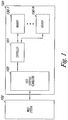
- FIG. 1 is a functional block diagram of an electronic memory system 120 that can be operated in accordance with embodiments of the present disclosure.
- the memory system 120 can be a solid state drive (SSD), for example.
- the system 120 can include a memory controller 101, a host interface connector 103, and a number of memory arrays 130-1, ..., 130-N, e.g., a number of solid state memory arrays, such as a number of flash arrays, for instance.
- the interface 103 can be used to communicate information between the memory system 120 and another device such as a host system 102.
- Host system 102 can include a memory access device, e.g., a processor.
- a processor can intend one or more processors, such as a parallel processing system, coprocessors, etc. Examples of host systems include laptop computers, personal computers, digital cameras, digital recording and playback devices, PDAs, memory card readers, interface hubs, and the like.
- the interface 103 can be in the form of a standardized interface.
- the host interface connector 103 can be a serial advanced technology attachment (SATA), peripheral component interconnect express (PCIe), or a universal serial bus (USB), among other connectors and interfaces.
- SATA serial advanced technology attachment
- PCIe peripheral component interconnect express
- USB universal serial bus
- interface 103 can provide an interface for passing control, address, data, and other signals between the memory system 120 and a host system 102 having compatible receptors for the interface 103.
- the memory controller 101 can communicate with the arrays 130-1, ..., 130-N to sense, program, and erase data, among other operations.
- Memory controller 101 can have circuitry that may be one or more integrated circuits and/or discrete components.
- the circuitry in memory controller 101 may include control circuitry for controlling access across a number of memory arrays and/or for providing a translation layer between an external host and the memory system 120.
- a memory controller could selectively couple an I/0 connection (not shown in Figure 1 ) of a memory array to receive the appropriate signal at the appropriate 1/0 connection at the appropriate time.
- the communication protocol between a host 102 and the memory system 120 may be different than what is required for access of a memory array, such as arrays 130-1 to 130-N.
- Memory controller 101 could then translate the commands received from a host, e.g., 102, into the appropriate commands to achieve the desired access to a memory array.
- Memory arrays 130-1, ..., 130-N can be arrays of non-volatile memory cells, which can be flash memory cells with a NAND architecture, for example.
- a NAND architecture the control gates of memory cells of a "row” can be coupled with a word line, while the drain regions of the memory cells of a "column” can be coupled to bit lines.
- the source regions of the memory cells can be coupled to source lines.
- the manner of connection of the memory cells to the bit lines and source lines depends on whether the array is a NAND architecture, a NOR architecture, an AND architecture, or some other memory array architecture.
- the memory system of Figure 1 can include additional circuitry that is not illustrated so as not to obscure embodiments of the present disclosure.
- the memory system 120 can include address circuitry to latch address signals provided over 110 connections through 1/0 circuitry. Address signals can be received and decoded by a row decoder and a column decoder to access the memory 130-1, ..., 130-N. It will be appreciated by those skilled in the art that the number of address input connections depends on the density and architecture of the memory 130-1, ..., 130-N, and that the number of addresses increases with both increased numbers of memory cells and increased numbers of memory blocks and arrays.
- FIG. 2 illustrates a diagram of a portion of a memory array 230 in accordance with an embodiment of the present disclosure. Although not shown in Figure 2 , one of ordinary skill in the art will appreciate that the memory array 230 can be located on a particular semiconductor die along with various peripheral circuitry associated with the operation thereof.
- array 230 has a number of physical blocks 240-0 (BLOCK 0), 240-1 (BLOCK 1), ..., 240-M (BLOCK M) of memory cells.
- the indicator "M" is used to indicate that the array 230 can include a number of physical blocks.
- the memory cells can be single level cells and/or multilevel cells.
- the number of physical blocks in array 230 maybe 128 blocks, 512 blocks, or 1,024 blocks, but embodiments are not limited to a particular multiple of 128 or to any particular number of physical blocks in an array 230. Further, embodiments are not limited to the type of memory used in the array, e.g., non-volatile, volatile, etc.
- the memory array 230 can be, for example, a NAND flash memory array 230.
- each physical block 240-0, 240-1, ..., 240-M includes memory cells which can be erased together as a unit, e.g., the cells in each physical block can be erased in a substantially simultaneous manner. For instance, the cells in each physical block can be erased together in a single operation.
- Each physical block, e.g., 240-0, 240-1, ..., 240-M contains a number of physical rows, e.g., 250-0, 250-1, ..., 250-R, of memory cells coupled to an access line, e.g., a word line.
- the indicator "R” is used to indicate that a physical block, e.g., 240-0, 240-1, ..., 240-M, can include a number of rows.
- the number of rows, e.g., word lines, in each physical block can be 32, but embodiments are not limited to a particular number of rows 250-0, 250-1, ..., 250-R per physical block.
- each row 250-0, 250-1, ..., 250-R can store one or more pages of data.
- a page refers to a unit of programming and/or reading, e.g., a number of cells that are programmed and/or read together or as a functional group of memory cells.
- each row 250-0, 250-1, ..., 250-R stores one page of data.
- each row can store multiple pages of data.
- each cell in a row can contribute a bit towards an upper page of data, and can contribute a bit towards a lower page of data.
- the memory array can include multiple physical blocks of memory cells and each physical block can be organized into multiple pages.
- a row such as row 250-0
- the indicator "S" is used to indicate that a row, e.g., 250-0, 250-1, ..., 250-R, can include a number of physical sectors.
- Each physical sector 252-0, 252-1, ..., 252-S can store data corresponding to a logical sector and can include overhead information, such as error correction code (ECC) information and logical block address (LBA) information, as well as user data.
- ECC error correction code
- LBA logical block address
- logical block addressing is a scheme often used by a host for identifying a logical sector of information.
- a logical sector of data can be a number of bytes of data, e.g., 256 bytes, 512 bytes, or 1,024 bytes. Embodiments are not limited to these examples.
- the physical blocks 240-0, 240-1, ..., 240-M rows 250-0, 250-1, ..., 250-R, sectors 252-0, 252-1, ..., 252-S, and pages are possible.
- the rows 250-0,250-1, ..., 250-R of the physical blocks 240-0, 240-1, ..., 240-M can each store data corresponding to a single logical sector which can include, for example, more or less than 512 bytes of data.
- Figure 3 illustrates a diagram of a file system for a number of memory arrays 330.
- a number of physical blocks can be used to store system data and a number of physical blocks can be used to store user data.
- the system data can include a partition boot record (PBR) 364, reserved data 366, a first file allocation table 368, and a second file allocation table 370.
- System data can include data that relates to the structure and operation of file system for a number of memory arrays 330.
- file allocation tables e.g., 368 and 370, can contain file allocation data that centralizes the information about which areas of memory arrays, e.g., 330, have data stored, are free or possibly unusable, and where data is stored in the memory array.
- Two file allocation tables can be used with one of the file allocation tables acting as a backup for a potential failure of one of the file allocation tables.
- the reserved data 366 can include data containing information about the memory arrays and can be used by the memory arrays to enable the operation of the memory arrays.
- user data can be, e.g., data received from a host device, such as host 102 shown in Figure 1 .
- the user data 362 can be written, read, and erased a number of times.
- a host device such as host 102, and/or control circuitry in a controller, such as controller 101, for example, can communicate commands to a memory array such that data is written to the memory array in a desired manner.
- the commands from the host device and/or control circuitry can be configured to write data at the beginning of a page for the data that is associated with each command.
- commands from the host device and/or control circuitry can be configured to write data at a first page of a physical block, e.g., physical block boundary, when writing data to an erased block.
- a formatted memory device can use the command from the host device and/or control circuitry to write data to the first memory cell of a page, e.g., page boundary, of a memory array and/or by writing data to the beginning of an empty, e.g., erased, page.
- Formatting the memory arrays can include writing PBR data, where the PBR can allocate space in the memory arrays for the system and user data.
- the PBR data structures can be constructed and/or configured such that user and system data starts at the beginning of a physical block.
- the PBR causes the command to write data at the next available location in the memory array corresponding to the modulus, which is calculated to ensure each modulus increment in the memory array is at the beginning of a physical block and/or page.
- Formatting includes using system data and/or metadata for the memory arrays to determine the location of the system data and user data in the memory arrays.
- System data and/or metadata can include physical parameters, such as memory array size, page size, block size, file system type, media type, and memory cell type, among other parameters.
- the storage space, e.g., sectors, that is available to store user data can be quantized to allocation units.
- An allocation unit, e.g., cluster can include a number of sectors. The number of sectors in an allocation unit can be specified by the system data and/or metadata for the memory arrays.
- a sector in the memory arrays can be comprised of 512 bytes and an allocation unit can have 8 sectors resulting in an allocation unit with 4096 bytes. Therefore, in this example, successive allocation units each containing 4096 bytes can be addressed by the host by adding 8 to the previous allocation unit's logical address.
- the minimum quantity of sectors for a write operation which is the number of sectors in a page, e.g. page size
- the minimum quantity of pages for an erase operation which is the number of pages in a block, e.g., block size
- the modulus can be used to format the memory array to determine the starting location for the components of the system data and the user data.
- an SSD can have 4, 8, or 16 sectors in a page, where a sector can be 512 bytes, and an SSD can have 128, 256, or 512 pages per physical block, therefore physical block sizes are 131072 bytes, 262144 bytes, and 524288 bytes.
- Embodiments of the present disclosure are not limited to this example and sectors, pages, and physical blocks can be comprised of any number of bytes.
- Formatting the memory arrays can include using the page size, block size, and allocation unit to determine the modulus to use when determining the starting location for the components of the system data and the user data.
- the host can use knowledge of the SSD's organization of the memory arrays, in particular those requirements that affect the minimum size of a write or erase operation, as well as the host's knowledge of metadata structures of the chosen file system, such as the size of FAT1 and FAT2, for example, employed to determine the format, e.g., the location of the components of the system data and the user data, for the memory arrays.
- the starting location for the PBR, reserved data, FAT1, FAT2, and user data can be defined using the modulus and the metadata and/or system data for the memory arrays. This formatting will align each of these portions at the beginning of a physical block.
- host requests to read or write user data will be aligned with the modulus and the allocation unit.
- FAT type file systems will most commonly organize the allocation units into groups of 512 byte sectors in increasing powers of 2, starting with a 1:1 allocation unit to logical block mapping for small capacity devices, up to 64 sectors per allocation unit.
- the accesses by host will be seen to be at addresses that are modulus 64, with fixed offset added to the address that depends on the size of the preceding or interlaced system, e.g., metadata, entries.
- a formatted SSD can increase performance and prolongs the life of the SSD by minimizing the extra writes incurred by a non-aligned format.
- a format which results in the least amount of extra overhead and/or extra read/write operations that the device must perform when new data is written by host is desired.
- Memory arrays can be formatted by aligning the logical addresses of the components of the system data and the user data, e.g., allocation units, based on powers of 2.
- the memory array translation of the logical address received in a host command cannot add an additional offset to the received logical address, or if an offset is used, the additional offset must also be a power of 2.
- Formatting memory arrays by writing data as aforesaid can reduce the amount of operating overhead associated with writing new data on the memory arrays.
- Overhead can refer to a number of additional memory cells that have to copied or moved in addition to the memory cells addressed by the write command due to the non-alignment of the write command address with respect to the flash (page or block) address, due to the difference in size of the smallest writeable or erasable unit between the hard drive and SSD.
- the reduction in overhead can be based at least partially on the lack of a need to move partially written pages to write a new data string on a page because formatting the memory array will cause data to be written to the beginning of an empty, e.g., erased, page.
- logical and/or physical blocks and/or pages can be used more efficiently when memory arrays are formatted.
- a format that aligns allocation units and system data to logical page boundaries and/or logical block boundaries, e.g., erase block, can cause the logical address of host write commands to coincide with the boundaries of the physical blocks or pages. Formatting can cause data to be written to the beginning of an empty, e.g., erased, physical block, e.g., at the boundary of the physical block.
- the data in physical blocks and/or pages can be erased and rewritten less often in a formatted memory array because the logical address of the host write command will start at the beginning of the logical and/or physical page and/or block, which does not require moving or copying those sectors in the page and/or physical block that precedes the logical address indicated in the write command as in the case of an unaligned format.
- Wear leveling can increase the life of a solid state memory array since a solid state memory array can experience failure after a number of program and/or erase cycles.
- Wear leveling can include dynamic wear leveling to minimize the amount of valid blocks moved to reclaim a block.
- Dynamic wear leveling can include a technique called garbage collection in which blocks with a number of invalid pages (i.e., pages with data that has been re-written to a different page and/or is no longer needed on the invalid pages) are reclaimed by erasing the block.
- Static wear leveling includes writing static data to blocks that have high erase counts to prolong the life of the block.
- a number of blocks can be designated as spare blocks to reduce the amount of write amplification associated with writing data in the memory array.
- a spare block can be a block in a memory array that can be designated as a block where data cannot be written.
- Write amplification is a process that occurs when writing data to solid state memory arrays. When randomly writing data in a memory array, the memory array scans for free space in the array. Free space in a memory array can be individual cells, pages, and/or blocks of memory cells that are not programmed. If there is enough free space to write the data, then the data is written to the free space in the memory array.
- the data in the memory array is rearranged by erasing, moving, and rewriting the data that is already present in the memory array to a new location leaving free space for the new data that is to be written in the memory array.
- the rearranging of old data in the memory array can be called write amplification because the amount of writing the memory arrays has to do in order to write new data is amplified based upon the amount of free space in the memory array and the size of the new data that is to be written on the memory array.
- Write amplification can be reduced by increasing the amount of space on a memory array that is designated as free space (i.e., where static data will not be written), thus allowing for less amplification of the amount of data that has to be written because less data will have to be rearranged.
- Memory array formatting can be used to reduce the amount of write amplification and also reduce the amount of designated free space needed to control write amplification to desired levels. Formatted memory arrays are filled with data in an efficient manner, starting at the boundaries of physical block and pages, therefore a data string in a formatted memory array will not start in the middle of a physical block and/or page, thus decreasing the chance that the data string will need to be rewritten to another location to free up space in the memory array for new data.
- Figure 4 illustrates a diagram of a file system for a number of memory arrays 430 having user data aligned at a block boundary.
- the file system for a number of memory arrays 430 includes a partition boot record 464, reserved data 466, a first file allocation table 468 (FILE ALLOCATION TABLE 1), and a second file allocation table 470 (FILE ALLOCATION TABLE 2).
- the reserved portion 466 and first file allocation table 468 are separated by padding 472.
- Padding 472 can be a number of memory cells that are not used to store system data or user data, e.g., the cells of padding 472 can remain in an erased state.
- the padding 472 can be located within memory arrays 430 such that the second file allocation table 470 ends at a block boundary, e.g., 474. Also, the padding 472 can be located within memory arrays 430 such that user data 462 starts at a block boundary, e.g., 474. The user data 462 can be aligned with a block boundary and the user data can be started at a physical block boundary in the memory arrays 430.
- the system data and the user data that is written to the solid state drive can be aligned with the physical structure of the solid state drive. That is, data is written at the beginning of a physical block when writing to an erased block and data is written at the beginning of a page when writing to an erased page. Also, data will not be written to a partially written page and the data will be written to the next available erased page.
- Various physical parameters associated with the memory arrays in a solid state drive can be stored in memory, such as random access memory (RAM), among other memory types, on the solid state drive and can be communicated to control circuitry in the solid state drive via the memory on the solid state drive.
- the various physical parameters can be communicated from a host device, which received the physical parameters from the memory on the solid state drive.
- the physical parameters can include memory array size, page size, block size, file system type, media type and memory cell type, among other parameters.
- a modulus for writing data to the memory arrays can be calculated by the control circuitry or the host device.
- the modulus can be the minimum incremental number of memory cells used when writing data.
- the modulus can be calculated based on the total number of memory cells, the block size, the page size, and the memory cell type of the memory arrays.
- Each portion of the solid state drive can be aligned with the physical parameters of the solid state drive.
- Padding e.g., padding 472
- the padding can be a number of cells that remain unused, e.g., cells left in an erased state and are not used to write data.
- Padding can be provided between reserved data and the file allocation table of the solid state drive. For instance, in the file system illustrated in Figure 4 , padding 472 is provided between reserved data 466 and file allocation table 468. Padding can be located such that the file allocation tables end at a block boundary, e.g., 474, thus aligning the start of the user data to the beginning of the block following the block boundary where the file allocation table ends.
- Padding can be provided between the reserved data and the first file allocation table causing the start of the first file allocation table to be aligned with a block boundary. Padding can be provided between the first file allocation table and the second file allocation table causing the second file allocation table to be aligned with a block boundary. In various embodiments, padding can be provided between the second file allocation table and the user data causing the user data to be aligned with a block boundary. Padding can be used, e.g., located, in various other locations within the memory arrays such that a portion of data on the solid state drive aligns with a block boundary.
- Figure 5 illustrates a diagram of a file system for a number of memory arrays 530 with the file allocation tables and user data aligned at a block boundary operated in accordance with a preferred embodimentof the present invention.
- the file system for a number of memory arrays 530 has a partition boot record 564, reserved data 566, a first file allocation table 568 (FILE ALLOCATION TABLE 1), and a second file allocation table 570 (FILE ALLOCATION TABLE 2).
- the reserved data 566 and the first file allocation table 568 are separated by padding 576.
- Padding 576 can be padding such as padding 472 described in connection with Figure 4 .
- padding 576 can be a number of memory cells that are not used to store data, e.g., data is not written to or read from the cells.
- the memory cells that are part of padding 576 end at block boundary 578 such that the first file allocation table 568 starts at a block boundary 578.
- the file allocation data that is written in the first file allocation table 568 can be aligned with the beginning of the block following boundary 578, as illustrated in Figure 5 .
- the first file allocation table 568 and the second file allocation table 570 are separated by padding 580.
- the memory cells that are part of padding 580 end at block boundary 582 such that the second file allocation table 570 starts at block boundary 582.
- the second file allocation table 570 and the user data 562 are separated by padding 584.
- the memory cells that are part of padding 584 are located such that user data 562 starts at block boundary 586.
- the user data 562 can be aligned with a block boundary and the user data can be started at a physical block boundary in the memory arrays 530.
- One device includes control circuitry coupled to a number of memory arrays, wherein each memory array has multiple physical blocks of memory cells.
- the memory arrays are formatted by the control circuitry that is configured to write system data to the number of memory arrays, where the system data ends at a physical block boundary; and write user data to the number of memory arrays, where the user data starts at a physical block boundary.
Landscapes
- Engineering & Computer Science (AREA)
- Theoretical Computer Science (AREA)
- Physics & Mathematics (AREA)
- General Engineering & Computer Science (AREA)
- General Physics & Mathematics (AREA)
- Human Computer Interaction (AREA)
- Memory System (AREA)
- Read Only Memory (AREA)
- Techniques For Improving Reliability Of Storages (AREA)
Description
- The present disclosure relates generally to semiconductor memory devices, methods, and systems, and more particularly, to solid state drive formatting.
- Memory devices are typically provided as internal, semiconductor, integrated circuits in computers or other electronic devices. There are many different types of memory including volatile and non-volatile memory. Volatile memory can require power to maintain its data and includes random-access memory (RAM), dynamic random access memory (DRAM), and synchronous dynamic random access memory (SDRAM), among others. Non-volatile memory can provide persistent data by retaining stored information when not powered and can include NAND flash memory, NOR flash memory, read only memory (ROM), Electrically Erasable Programmable ROM (EEPROM), Erasable Programmable ROM (EPROM), and phase change random access memory (PCRAM), among others.
- Memory devices can be combined together to form a solid state drive (SSD). A solid state drive can include non-volatile memory, e.g., NAND flash memory and NOR flash memory, and/or can include volatile memory, e.g., DRAM and SRAM, among various other types of non-volatile and volatile memory.
- An SSD can be used to replace hard disk drives as the main storage device for a computer, as the solid state drive can have advantages over hard drives in terms of performance, size, weight, ruggedness, operating temperature range, and power consumption. For example, SSDs can have superior performance when compared to magnetic disk drives due to their lack of moving parts, which may ameliorate seek time, latency, and other electromechanical delays associated with magnetic disk drives. SSD manufacturers can use non-volatile flash memory to create flash SSDs that may not use an internal battery supply, thus allowing the drive to be more versatile and compact.
- An SSD can include a number of memory devices, e.g., a number of memory chips (as used herein, "a number of' something can refer to one or more of such things, e.g., a number of memory devices can refer to one or more memory devices). As one of ordinary skill in the art will appreciate, a memory chip can include a number of dies. Each die can include a number of memory arrays and peripheral circuitry thereon. The memory arrays can include a number of memory cells organized into a number of physical blocks, and the physical blocks can be organized into a number of pages.
- For some storage applications, SSDs can be used as a replacement or compliment to hard (disk) drives. In these instances, SSDs are placed in an environment that was designed to accommodate a hard drive's functions. Due to the differences in granularity or quantization of the smallest erasable unit between SSDs and hard drives (e.g., a 512 byte sector for hard drives versus a 128k or 256k block in SSDs), an SSD that is used as a replacement for or compliment to a hard drive in a computing device may not operate at peak performance levels.
- United States Patent Application Publication No.
2008/002467 A1 entitled "Card Controller Controlling Semiconductor Memory Including Memory Cell Having Charge Accumulation Layer and Control Gate" by Tsuji, Hidetaka describes a card controller that includes an arithmetic processing device. The controller writes data to a semiconductor memory having a first memory block and a second memory block each including a plurality of nonvolatile memory cells each configured to hold at least 2 bits, data in the first memory block and data in the second memory block being each erased at a time. The arithmetic processing device writes the data to the memory cells in the first memory block using an upper bit and a lower bit of the at least 2 bits and writes the data to the memory cells in the second memory block using only the lower bit of the at least 2 bits. - United States Patent Application Publication No.
US 2007/234297 A1 entitled "Software Robustness through Search for Robust Runtime Implementations" by Zorn, Benjamin et. al describes software program robustness that is improved by successfully masking memory safety errors in the software program. For instance, at least some memory safety errors in a software program can be masked by using a runtime memory manager that approximates the semantics of an infinite heap memory manager. In one example, an approximation of an infinite heap memory manager is implemented by configuring a parameterized memory manager with parameter values such as padding to be added to each allocation on the heap and the amount of deferment before executing a call to free memory on the heap. Ideal configurations balance expected robustness with costs such as added memory and processing time. Ideal configurations can be identified through systematic search of a coordinate space of selected parameters. Ideal configurations can also be identified by statistically correlating success/failure data collected from execution of deployed instances of the software program to the configuration of the memory managers used therein. - United States Patent No.
5,799,168 entitled "Standardised Flash Controller" by Ban, Amir describes a flash memory controller that operates a flash memory array comprising a plurality of different types of flash memory chips. The CPU interacts with the array by issuing generic commands through a single Memory Technology Driver (MTD), while the controller translates the generic commands into commands specific to the chip comprising the portion of the array being addressed. The controller operates each of the flash chips which comprises the flash memory array, and presents to the CPU a memory system comprised of a single addressable entity. According to a further feature of this document, the controller is embedded into each of the flash chips in an array in order to further reduce overhead costs. - United States Patent Application Publication No.
US 2006/0004969 A1 entitled "High-Speed Accessible Memory Featuring Reduced Data Movement" by Suda, Takaya describes a control section that includes an address information detection section detecting address information from a write command including address information, an address information storage section storing address information, and a first address determination section determining whether or not the address information detected by the address information detection section matches with the address information stored in the address information storage section. The control section stores directory entry information corresponding to the address information in the second storage section when receiving matching information from the first address determination section. - United State Patent No.
6191712 B1 entitled "Circuit for Aligning Logical Sectors with Physical Sectors in a Disk Storage System" by Still, Charles Lee, discloses including padding data to the end of each logical sector so that, when data is written to the memory cells, a logical sector of data will completely fill a physical sector of data and therefore the next logical sector of data when written will start at the beginning of the next physical sector. The padding of memory cells is used in each physical sector. Every write operation includes data padding. - The invention is set out in the appended claims. There is disclosed a memory controller, comprising:
- control circuitry coupled to a number of memory arrays, wherein each memory array has multiple physical blocks of memory cells and wherein each memory array is formatted by the control circuitry that is configured to:
- write system data to the number of memory arrays such that data in a first file allocation table of the system data is continuous and starts at a beginning of a first physical block in the number of memory arrays by including a first padding of memory cells that do not contain data after reserved data of the system data;
- write system data to the number of memory arrays such that data in a second file allocation table of the system data is continuous and starts at the beginning of a second physical block in the number of memory arrays by including a second padding of memory cells that do not contain data after the first file allocation table; and
- write user data to the number of memory arrays such that the user data starts at a beginning of a third physical block in the number of memory arrays by including a third padding of memory cells that do not contain data after the second file allocation table, wherein the first block, the second block and the third block are discrete respective blocks. There is disclosed a memory system comprising the cooperative combination of:
- the memory controller just described; and
- the number of memory arrays.
- According to yet another aspect of the invention there is disclosed a method for formatting a number of memory arrays in a memory system, the method comprising: indicating physical parameters associated with the number of memory arrays; allocating a number of memory cells in the number of memory arrays for storing system data; allocating a number of memory cells in the number of memory arrays for storing user data; writing system data to the number of memory cells in the number of memory arrays such that data in a first file allocation table of the system data is continuous and starts at the beginning of a first physical block in the number of memory arrays by including first, wherein writing system data includes a padding of erased memory cells after reserved data of the system data that separates a first portion of the system data from a second portion of the system data such that one of a number of file allocation tables of the system data ends at a physical block boundary of a first block; writing system data to the number of memory cells in the number of memory arrays such that data in a second allocation table of the system data is continuous and starts at the beginning of a second physical block in the number of memory arrays by including a second padding of erased memory cells after the first file allocation table; and writing user data 362such that the user data starts at the a beginning of a third physical block boundary of a second block of the number of memory cells in the number of memory arrays by including a third padding of erased memory cells after the second file allocation table, wherein the first block, is a different block than the second block and the third block are respective discrete blocks.
-
-
FIG. 1 is a functional block diagram of an electronic memory system that can be operated in accordance with one or more embodiments of the present invention; disclosure. -
FIG. 2 illustrates a diagram of a portion of a memory array in accordance with one or more embodiments of the present invention; -
FIG. 3 illustrates a diagram of a file system for a number of memory arrays, the description of which is included here by way of explanatory background; -
FIG. 4 illustrates a diagram of a file system for a number of memory arrays having user data aligned at a block boundary, the description of which is further included hereby by way of explanatory background; -
FIG. 5 illustrates a diagram of a file system for a number of memory arrays with the file allocation tables and user data aligned at a block boundary in accordance with a preferred embodiment of the present invention. - The present disclosure includes methods and devices for solid state drive formatting. One device embodiment includes control circuitry coupled to a number of memory arrays, wherein each memory array has multiple physical blocks of memory cells. The memory arrays can be formatted by the control circuitry that is configured to write system data to the number of memory arrays such that the system data ends at a physical block boundary and to write user data to the number of memory arrays such that the user data starts at a physical block boundary.
- In the following detailed description, reference is made to the accompanying drawings that form a part hereof, and in which is shown by way of illustration how explanatory examples and embodiments may be practised. The preferred embodiment is described in sufficient detail to enable those of ordinary skill in the art to practice the same, and it is to be understood that other embodiments may be utilized and that process, electrical, and/or structural changes may be made without departing from the scope of the present disclosure. As used herein, the designators "N," "M," "R," and "S," particularly with respect to reference numerals in the drawings, indicates that a number of the particular feature so designated can be included with one or more embodiments of the present invention.
- The figures herein follow a numbering convention in which the first digit or digits correspond to the drawing figure number and the remaining digits identify an element or component in the drawing. Similar elements or components between different figures may be identified by the use of similar digits. For example, 130 may reference element "30" in
Figure 1 , and a similar element may be referenced as 230 inFigure 2 . As will be appreciated, elements shown in the examples and in the preferred embodiment herein can be added, exchanged, and/or eliminated so as to provide a number of additional examples and embodiments. In addition, as will be appreciated, the proportion and the relative scale of the elements provided in the figures are intended by way of illustration, and should not be taken in a limiting sense. -
Figure 1 is a functional block diagram of anelectronic memory system 120 that can be operated in accordance with embodiments of the present disclosure. In the embodiment illustrated inFigure 1 , thememory system 120 can be a solid state drive (SSD), for example. As illustrated inFigure 1 , thesystem 120 can include amemory controller 101, ahost interface connector 103, and a number of memory arrays 130-1, ..., 130-N, e.g., a number of solid state memory arrays, such as a number of flash arrays, for instance. - The
interface 103 can be used to communicate information between thememory system 120 and another device such as ahost system 102.Host system 102 can include a memory access device, e.g., a processor. One of ordinary skill in the art will appreciate that "a processor" can intend one or more processors, such as a parallel processing system, coprocessors, etc. Examples of host systems include laptop computers, personal computers, digital cameras, digital recording and playback devices, PDAs, memory card readers, interface hubs, and the like. For one or more embodiments, theinterface 103 can be in the form of a standardized interface. For example, thehost interface connector 103 can be a serial advanced technology attachment (SATA), peripheral component interconnect express (PCIe), or a universal serial bus (USB), among other connectors and interfaces. In general, however,interface 103 can provide an interface for passing control, address, data, and other signals between thememory system 120 and ahost system 102 having compatible receptors for theinterface 103. - The
memory controller 101 can communicate with the arrays 130-1, ..., 130-N to sense, program, and erase data, among other operations.Memory controller 101 can have circuitry that may be one or more integrated circuits and/or discrete components. - The circuitry in
memory controller 101 may include control circuitry for controlling access across a number of memory arrays and/or for providing a translation layer between an external host and thememory system 120. Thus, a memory controller could selectively couple an I/0 connection (not shown inFigure 1 ) of a memory array to receive the appropriate signal at the appropriate 1/0 connection at the appropriate time. Similarly, the communication protocol between ahost 102 and thememory system 120 may be different than what is required for access of a memory array, such as arrays 130-1 to 130-N. Memory controller 101 could then translate the commands received from a host, e.g., 102, into the appropriate commands to achieve the desired access to a memory array. - Memory arrays 130-1, ..., 130-N can be arrays of non-volatile memory cells, which can be flash memory cells with a NAND architecture, for example. In a NAND architecture, the control gates of memory cells of a "row" can be coupled with a word line, while the drain regions of the memory cells of a "column" can be coupled to bit lines. The source regions of the memory cells can be coupled to source lines. As will be appreciated by those of ordinary skill in the art, the manner of connection of the memory cells to the bit lines and source lines depends on whether the array is a NAND architecture, a NOR architecture, an AND architecture, or some other memory array architecture.
- The memory system of
Figure 1 can include additional circuitry that is not illustrated so as not to obscure embodiments of the present disclosure. For example, thememory system 120 can include address circuitry to latch address signals provided over 110 connections through 1/0 circuitry. Address signals can be received and decoded by a row decoder and a column decoder to access the memory 130-1, ..., 130-N. It will be appreciated by those skilled in the art that the number of address input connections depends on the density and architecture of the memory 130-1, ..., 130-N, and that the number of addresses increases with both increased numbers of memory cells and increased numbers of memory blocks and arrays. -
Figure 2 illustrates a diagram of a portion of amemory array 230 in accordance with an embodiment of the present disclosure. Although not shown inFigure 2 , one of ordinary skill in the art will appreciate that thememory array 230 can be located on a particular semiconductor die along with various peripheral circuitry associated with the operation thereof. - As shown in
Figure 2 ,array 230 has a number of physical blocks 240-0 (BLOCK 0), 240-1 (BLOCK 1), ..., 240-M (BLOCK M) of memory cells. In the example shown inFigure 1 , the indicator "M" is used to indicate that thearray 230 can include a number of physical blocks. The memory cells can be single level cells and/or multilevel cells. As an example, the number of physical blocks inarray 230 maybe 128 blocks, 512 blocks, or 1,024 blocks, but embodiments are not limited to a particular multiple of 128 or to any particular number of physical blocks in anarray 230. Further, embodiments are not limited to the type of memory used in the array, e.g., non-volatile, volatile, etc. In the embodiment illustrated inFigure 2 , thememory array 230 can be, for example, a NANDflash memory array 230. - In this example, each physical block 240-0, 240-1, ..., 240-M includes memory cells which can be erased together as a unit, e.g., the cells in each physical block can be erased in a substantially simultaneous manner. For instance, the cells in each physical block can be erased together in a single operation. Each physical block, e.g., 240-0, 240-1, ..., 240-M, contains a number of physical rows, e.g., 250-0, 250-1, ..., 250-R, of memory cells coupled to an access line, e.g., a word line. The indicator "R" is used to indicate that a physical block, e.g., 240-0, 240-1, ..., 240-M, can include a number of rows. In some embodiments, the number of rows, e.g., word lines, in each physical block can be 32, but embodiments are not limited to a particular number of rows 250-0, 250-1, ..., 250-R per physical block.
- As one of ordinary skill in the art will appreciate, each row 250-0, 250-1, ..., 250-R can store one or more pages of data. A page refers to a unit of programming and/or reading, e.g., a number of cells that are programmed and/or read together or as a functional group of memory cells. In the embodiment shown in
Figure 1 , each row 250-0, 250-1, ..., 250-R stores one page of data. However, embodiments of the present disclosure are not so limited. For instance, in some embodiments of the present disclosure, each row can store multiple pages of data. For example, each cell in a row can contribute a bit towards an upper page of data, and can contribute a bit towards a lower page of data. The memory array can include multiple physical blocks of memory cells and each physical block can be organized into multiple pages. - In one or more embodiments of the present disclosure, and as shown in
Figure 2 , a row, such as row 250-0, can store data in accordance with a number of physical sectors 252-0, 252-1, ..., 252-S. The indicator "S" is used to indicate that a row, e.g., 250-0, 250-1, ..., 250-R, can include a number of physical sectors. Each physical sector 252-0, 252-1, ..., 252-S can store data corresponding to a logical sector and can include overhead information, such as error correction code (ECC) information and logical block address (LBA) information, as well as user data. As one of ordinary skill in the art will appreciate, logical block addressing is a scheme often used by a host for identifying a logical sector of information. As an example, a logical sector of data can be a number of bytes of data, e.g., 256 bytes, 512 bytes, or 1,024 bytes. Embodiments are not limited to these examples. - It is noted that other configurations for the physical blocks 240-0, 240-1, ..., 240-M, rows 250-0, 250-1, ..., 250-R, sectors 252-0, 252-1, ..., 252-S, and pages are possible. For example, the rows 250-0,250-1, ..., 250-R of the physical blocks 240-0, 240-1, ..., 240-M can each store data corresponding to a single logical sector which can include, for example, more or less than 512 bytes of data.
-
Figure 3 illustrates a diagram of a file system for a number ofmemory arrays 330. A number of physical blocks can be used to store system data and a number of physical blocks can be used to store user data. InFigure 3 , the system data can include a partition boot record (PBR) 364, reserveddata 366, a first file allocation table 368, and a second file allocation table 370. System data can include data that relates to the structure and operation of file system for a number ofmemory arrays 330. As an example, file allocation tables, e.g., 368 and 370, can contain file allocation data that centralizes the information about which areas of memory arrays, e.g., 330, have data stored, are free or possibly unusable, and where data is stored in the memory array. Two file allocation tables can be used with one of the file allocation tables acting as a backup for a potential failure of one of the file allocation tables. Thereserved data 366, for example, can include data containing information about the memory arrays and can be used by the memory arrays to enable the operation of the memory arrays. - In the file system illustrated in
Figure 3 , user data can be, e.g., data received from a host device, such ashost 102 shown inFigure 1 . Theuser data 362 can be written, read, and erased a number of times. - A host device, such as
host 102, and/or control circuitry in a controller, such ascontroller 101, for example, can communicate commands to a memory array such that data is written to the memory array in a desired manner. The commands from the host device and/or control circuitry can be configured to write data at the beginning of a page for the data that is associated with each command. Also, commands from the host device and/or control circuitry can be configured to write data at a first page of a physical block, e.g., physical block boundary, when writing data to an erased block. A formatted memory device can use the command from the host device and/or control circuitry to write data to the first memory cell of a page, e.g., page boundary, of a memory array and/or by writing data to the beginning of an empty, e.g., erased, page. - Formatting the memory arrays can include writing PBR data, where the PBR can allocate space in the memory arrays for the system and user data. The PBR data structures can be constructed and/or configured such that user and system data starts at the beginning of a physical block. When a write command is received by the memory arrays, the PBR causes the command to write data at the next available location in the memory array corresponding to the modulus, which is calculated to ensure each modulus increment in the memory array is at the beginning of a physical block and/or page.
- Formatting includes using system data and/or metadata for the memory arrays to determine the location of the system data and user data in the memory arrays. System data and/or metadata can include physical parameters, such as memory array size, page size, block size, file system type, media type, and memory cell type, among other parameters. The storage space, e.g., sectors, that is available to store user data can be quantized to allocation units. An allocation unit, e.g., cluster, can include a number of sectors. The number of sectors in an allocation unit can be specified by the system data and/or metadata for the memory arrays. F or example, a sector in the memory arrays can be comprised of 512 bytes and an allocation unit can have 8 sectors resulting in an allocation unit with 4096 bytes. Therefore, in this example, successive allocation units each containing 4096 bytes can be addressed by the host by adding 8 to the previous allocation unit's logical address.
- The minimum quantity of sectors for a write operation, which is the number of sectors in a page, e.g. page size, and/or the minimum quantity of pages for an erase operation, which is the number of pages in a block, e.g., block size, can be used along with the allocation unit, as defined by the memory array metadata and/or system data, to determine the modulus for the memory arrays. The modulus can be used to format the memory array to determine the starting location for the components of the system data and the user data.
- For example, an SSD can have 4, 8, or 16 sectors in a page, where a sector can be 512 bytes, and an SSD can have 128, 256, or 512 pages per physical block, therefore physical block sizes are 131072 bytes, 262144 bytes, and 524288 bytes. Embodiments of the present disclosure are not limited to this example and sectors, pages, and physical blocks can be comprised of any number of bytes.
- Formatting the memory arrays can include using the page size, block size, and allocation unit to determine the modulus to use when determining the starting location for the components of the system data and the user data. During formatting the host can use knowledge of the SSD's organization of the memory arrays, in particular those requirements that affect the minimum size of a write or erase operation, as well as the host's knowledge of metadata structures of the chosen file system, such as the size of FAT1 and FAT2, for example, employed to determine the format, e.g., the location of the components of the system data and the user data, for the memory arrays. For example, the starting location for the PBR, reserved data, FAT1, FAT2, and user data can be defined using the modulus and the metadata and/or system data for the memory arrays. This formatting will align each of these portions at the beginning of a physical block.
- Once the device has been formatted, host requests to read or write user data will be aligned with the modulus and the allocation unit. For example, FAT type file systems will most commonly organize the allocation units into groups of 512 byte sectors in increasing powers of 2, starting with a 1:1 allocation unit to logical block mapping for small capacity devices, up to 64 sectors per allocation unit. For example, in the case of 64 sectors per allocation unit, the accesses by host will be seen to be at addresses that are modulus 64, with fixed offset added to the address that depends on the size of the preceding or interlaced system, e.g., metadata, entries.
- When the SSD receives a write command that is not aligned to a page boundary, those sectors in the page that precede the sector indicated by the starting logical block of the write command are copied to the page being accessed by the write command, resulting in extra overhead, and also more writes to the memory arrays, as the old location of those sectors will also need to be erased. A formatted SSD can increase performance and prolongs the life of the SSD by minimizing the extra writes incurred by a non-aligned format.
- A format which results in the least amount of extra overhead and/or extra read/write operations that the device must perform when new data is written by host is desired.
- A host that has no knowledge of the SSD's page size and/or erase block size, e.g. metadata and/or system data, can format the memory arrays based on the fact that memory array capacities can be quantized to powers of 2. Memory arrays can be formatted by aligning the logical addresses of the components of the system data and the user data, e.g., allocation units, based on powers of 2. In a memory system that aligns system data and allocation units based on powers of 2, the memory array translation of the logical address received in a host command cannot add an additional offset to the received logical address, or if an offset is used, the additional offset must also be a power of 2.
- Formatting memory arrays by writing data as aforesaid can reduce the amount of operating overhead associated with writing new data on the memory arrays. Overhead can refer to a number of additional memory cells that have to copied or moved in addition to the memory cells addressed by the write command due to the non-alignment of the write command address with respect to the flash (page or block) address, due to the difference in size of the smallest writeable or erasable unit between the hard drive and SSD. The reduction in overhead can be based at least partially on the lack of a need to move partially written pages to write a new data string on a page because formatting the memory array will cause data to be written to the beginning of an empty, e.g., erased, page.
- Also, logical and/or physical blocks and/or pages can be used more efficiently when memory arrays are formatted. A format that aligns allocation units and system data to logical page boundaries and/or logical block boundaries, e.g., erase block, can cause the logical address of host write commands to coincide with the boundaries of the physical blocks or pages. Formatting can cause data to be written to the beginning of an empty, e.g., erased, physical block, e.g., at the boundary of the physical block. The data in physical blocks and/or pages can be erased and rewritten less often in a formatted memory array because the logical address of the host write command will start at the beginning of the logical and/or physical page and/or block, which does not require moving or copying those sectors in the page and/or physical block that precedes the logical address indicated in the write command as in the case of an unaligned format.
- Formatting a memory array can complement wear leveling that can be implemented to control the wear rate on the memory arrays (e.g. 130-1 ... 130-N in
Figure 1 ). As one of ordinary skill in the art will appreciate, wear leveling can increase the life of a solid state memory array since a solid state memory array can experience failure after a number of program and/or erase cycles. - Wear leveling can include dynamic wear leveling to minimize the amount of valid blocks moved to reclaim a block. Dynamic wear leveling can include a technique called garbage collection in which blocks with a number of invalid pages (i.e., pages with data that has been re-written to a different page and/or is no longer needed on the invalid pages) are reclaimed by erasing the block. Static wear leveling includes writing static data to blocks that have high erase counts to prolong the life of the block.
- Herein, a number of blocks can be designated as spare blocks to reduce the amount of write amplification associated with writing data in the memory array. A spare block can be a block in a memory array that can be designated as a block where data cannot be written. Write amplification is a process that occurs when writing data to solid state memory arrays. When randomly writing data in a memory array, the memory array scans for free space in the array. Free space in a memory array can be individual cells, pages, and/or blocks of memory cells that are not programmed. If there is enough free space to write the data, then the data is written to the free space in the memory array. If there is not enough free space in one location, the data in the memory array is rearranged by erasing, moving, and rewriting the data that is already present in the memory array to a new location leaving free space for the new data that is to be written in the memory array. The rearranging of old data in the memory array can be called write amplification because the amount of writing the memory arrays has to do in order to write new data is amplified based upon the amount of free space in the memory array and the size of the new data that is to be written on the memory array. Write amplification can be reduced by increasing the amount of space on a memory array that is designated as free space (i.e., where static data will not be written), thus allowing for less amplification of the amount of data that has to be written because less data will have to be rearranged.
- Memory array formatting can be used to reduce the amount of write amplification and also reduce the amount of designated free space needed to control write amplification to desired levels. Formatted memory arrays are filled with data in an efficient manner, starting at the boundaries of physical block and pages, therefore a data string in a formatted memory array will not start in the middle of a physical block and/or page, thus decreasing the chance that the data string will need to be rewritten to another location to free up space in the memory array for new data.
-
Figure 4 illustrates a diagram of a file system for a number ofmemory arrays 430 having user data aligned at a block boundary. InFigure 4 , the file system for a number ofmemory arrays 430 includes apartition boot record 464, reserveddata 466, a first file allocation table 468 (FILE ALLOCATION TABLE 1), and a second file allocation table 470 (FILE ALLOCATION TABLE 2). In the file system illustrated inFigure 4 , the reservedportion 466 and first file allocation table 468 are separated by padding 472. Padding 472 can be a number of memory cells that are not used to store system data or user data, e.g., the cells of padding 472 can remain in an erased state. The padding 472 can be located withinmemory arrays 430 such that the second file allocation table 470 ends at a block boundary, e.g., 474. Also, the padding 472 can be located withinmemory arrays 430 such thatuser data 462 starts at a block boundary, e.g., 474. Theuser data 462 can be aligned with a block boundary and the user data can be started at a physical block boundary in thememory arrays 430. - The system data and the user data that is written to the solid state drive can be aligned with the physical structure of the solid state drive. That is, data is written at the beginning of a physical block when writing to an erased block and data is written at the beginning of a page when writing to an erased page. Also, data will not be written to a partially written page and the data will be written to the next available erased page.
- Various physical parameters associated with the memory arrays in a solid state drive can be stored in memory, such as random access memory (RAM), among other memory types, on the solid state drive and can be communicated to control circuitry in the solid state drive via the memory on the solid state drive. In one or more embodiments, the various physical parameters can be communicated from a host device, which received the physical parameters from the memory on the solid state drive. The physical parameters can include memory array size, page size, block size, file system type, media type and memory cell type, among other parameters.
- Once the physical parameters are known by the control circuitry or by the host device, a modulus for writing data to the memory arrays can be calculated by the control circuitry or the host device. The modulus can be the minimum incremental number of memory cells used when writing data. The modulus can be calculated based on the total number of memory cells, the block size, the page size, and the memory cell type of the memory arrays.
- Each portion of the solid state drive can be aligned with the physical parameters of the solid state drive. Padding, e.g., padding 472, can be provided in between each portion of data on the solid state drive. The padding can be a number of cells that remain unused, e.g., cells left in an erased state and are not used to write data. Padding can be provided between reserved data and the file allocation table of the solid state drive. For instance, in the file system illustrated in
Figure 4 , padding 472 is provided betweenreserved data 466 and file allocation table 468. Padding can be located such that the file allocation tables end at a block boundary, e.g., 474, thus aligning the start of the user data to the beginning of the block following the block boundary where the file allocation table ends. - Padding can be provided between the reserved data and the first file allocation table causing the start of the first file allocation table to be aligned with a block boundary. Padding can be provided between the first file allocation table and the second file allocation table causing the second file allocation table to be aligned with a block boundary. In various embodiments, padding can be provided between the second file allocation table and the user data causing the user data to be aligned with a block boundary. Padding can be used, e.g., located, in various other locations within the memory arrays such that a portion of data on the solid state drive aligns with a block boundary.
-
Figure 5 illustrates a diagram of a file system for a number ofmemory arrays 530 with the file allocation tables and user data aligned at a block boundary operated in accordance with a preferred embodimentof the present invention. InFigure 5 , the file system for a number ofmemory arrays 530 has apartition boot record 564, reserveddata 566, a first file allocation table 568 (FILE ALLOCATION TABLE 1), and a second file allocation table 570 (FILE ALLOCATION TABLE 2). Thereserved data 566 and the first file allocation table 568 are separated bypadding 576. Padding 576 can be padding such as padding 472 described in connection withFigure 4 . For instance, padding 576 can be a number of memory cells that are not used to store data, e.g., data is not written to or read from the cells. The memory cells that are part ofpadding 576 end atblock boundary 578 such that the first file allocation table 568 starts at ablock boundary 578. The file allocation data that is written in the first file allocation table 568 can be aligned with the beginning of theblock following boundary 578, as illustrated inFigure 5 . - In
Figure 5 , the first file allocation table 568 and the second file allocation table 570 are separated bypadding 580. The memory cells that are part ofpadding 580 end atblock boundary 582 such that the second file allocation table 570 starts atblock boundary 582. - In
Figure 5 , the second file allocation table 570 and theuser data 562 are separated bypadding 584. The memory cells that are part ofpadding 584 are located such thatuser data 562 starts atblock boundary 586. Theuser data 562 can be aligned with a block boundary and the user data can be started at a physical block boundary in thememory arrays 530. - The present disclosure includes methods and devices for solid state drive formatting. One device includes control circuitry coupled to a number of memory arrays, wherein each memory array has multiple physical blocks of memory cells. The memory arrays are formatted by the control circuitry that is configured to write system data to the number of memory arrays, where the system data ends at a physical block boundary; and write user data to the number of memory arrays, where the user data starts at a physical block boundary.
- Although a preferred embodiment has been illustrated and described herein, those of ordinary skill in the art will appreciate that an arrangement calculated to achieve the same results can be substituted.
Claims (11)
- A memory controller (101), comprising:
control circuitry coupled to a number of memory arrays (130), wherein each memory array (130) has multiple physical blocks (240; 240-0, ... 240-M) of memory cells and wherein each memory array (130) is formatted by the control circuitry that is configured to:write system data (564, 566, 568, 570) to the number of memory arrays (130) such that data in a first file allocation table (568) of the system data is continuous and starts at a beginning (578) of a first physical block in the number of memory arrays by including a first padding (576, 580, 584) of memory cells that do not contain data after reserved data (566) of the system data;write system data to the number of memory arrays such that data in a second file allocation table (570) of the system data is continuous and starts at the beginning (582) of a second physical block in the number of memory arrays by including a second padding (580) of memory cells that do not contain data after the first file allocation table (568); andwrite user data (562) to the number of memory arrays such that the user data (562) starts at a beginning (586) of a third physical block in the number of memory arrays by including a third padding (584) of memory cells that do not contain data after the second file allocation table (570), wherein the first block, the second block and the third block are discrete respective blocks (240). - The memory controller (101) of claim 1, wherein the number of memory arrays (130) include a portion for system data (564, 566, 568, 570) and a portion for user data (562).
- The memory controller (101) of claim 1, wherein an indication of one or more physical parameters of the number of memory arrays (130) is stored in memory in the control circuitry.
- The memory controller (101) of claim 3, wherein the one or more physical parameters of the number of memory arrays (130) include array size, page size, block size, and memory cell type.
- The memory controller (101) of any one of claims 1-4, wherein the system data includes a partition boot record (564), the reserved data (566), the first file allocation table (568), and the second file allocation table (570).
- A memory system (120) comprising the cooperative combination of:said memory controller (101); andsaid member of memory array (130).
- A method for formatting a number of memory arrays (130) in a memory system (120), the method comprising:indicating physical parameters associated with the number of memory arrays (130);allocating a number of memory cells in the number of memory arrays (130) for storing system data (564, 566, 568, 570);allocating a number of memory cells in the number of memory arrays (130) for storing user data (562);writing system data to the number of memory cells in the number of memory arrays such that data in a first file allocation table (568) of the system data is continuous and starts at the beginning of a first physical block in the number of memory arrays by including first a padding (576) of erased memory cells after reserved data of the system data;writing system data to the number of memory cells in the number of memory arrays such that data in a second allocation table (570) of the system data is continuous and starts at the beginning (582) of a second physical block in the number of memory arrays by including a second padding (580) of erased memory cells after the first file allocation table (568); andwriting user data (562) such that the user data (562) starts at the beginning (586) of a third physical block in the number of memory arrays (130) by including a third padding (584) of erased memory cells after the second file allocation table (570), wherein the first block, the second block and the third block are respective discrete blocks (240).
- The method of claim 7, wherein the system data includes a partition boot record (564), the reserved data (566), the first file allocation table (568), and the second file allocation table (570).
- The method of claim 7, including indicating one or more physical parameters associated with the number of memory arrays (130) by receiving the physical parameters from a memory in a memory controller (101).
- The method of claim 7, including calculating a modulus for the number of memory arrays (130) based on the indicated physical parameters.
- The method of any one of claims 7-10, including storing one or more physical parameters associated with the number of memory arrays (130) in a memory in a memory controller (101).
Applications Claiming Priority (2)
| Application Number | Priority Date | Filing Date | Title |
|---|---|---|---|
| US12/356,725 US8392687B2 (en) | 2009-01-21 | 2009-01-21 | Solid state memory formatting |
| PCT/US2010/000099 WO2010090697A2 (en) | 2009-01-21 | 2010-01-15 | Solid state memory formatting |
Publications (3)
| Publication Number | Publication Date |
|---|---|
| EP2389631A2 EP2389631A2 (en) | 2011-11-30 |
| EP2389631A4 EP2389631A4 (en) | 2012-08-22 |
| EP2389631B1 true EP2389631B1 (en) | 2018-08-08 |
Family
ID=42337852
Family Applications (1)
| Application Number | Title | Priority Date | Filing Date |
|---|---|---|---|
| EP10738833.2A Active EP2389631B1 (en) | 2009-01-21 | 2010-01-15 | Solid state memory formatting |
Country Status (7)
| Country | Link |
|---|---|
| US (3) | US8392687B2 (en) |
| EP (1) | EP2389631B1 (en) |
| JP (1) | JP5823875B2 (en) |
| KR (3) | KR20140016440A (en) |
| CN (1) | CN102292711B (en) |
| TW (1) | TWI418980B (en) |
| WO (1) | WO2010090697A2 (en) |
Families Citing this family (26)
| Publication number | Priority date | Publication date | Assignee | Title |
|---|---|---|---|---|
| US8988800B1 (en) | 2009-09-15 | 2015-03-24 | Marvell International Ltd. | Error correction for storage devices |
| US8402217B2 (en) * | 2009-09-15 | 2013-03-19 | Marvell International Ltd. | Implementing RAID in solid state memory |
| US20120089765A1 (en) * | 2010-10-07 | 2012-04-12 | Huang Shih-Chia | Method for performing automatic boundary alignment and related non-volatile memory device |
| JP5395824B2 (en) * | 2011-02-16 | 2014-01-22 | 株式会社東芝 | Memory system |
| WO2012148812A2 (en) * | 2011-04-29 | 2012-11-01 | Lsi Corporation | Encrypted transport solid-state disk controller |
| JP2013077209A (en) * | 2011-09-30 | 2013-04-25 | Nintendo Co Ltd | Program, information processing system, information processing device, and information processing method |
| TWI467379B (en) * | 2012-04-23 | 2015-01-01 | Phison Electronics Corp | System operation method, and memory controller and memory storage device using the same |
| CN103383663B (en) * | 2012-05-04 | 2016-06-29 | 群联电子股份有限公司 | System operation method, memory controller and memory |
| US9645917B2 (en) * | 2012-05-22 | 2017-05-09 | Netapp, Inc. | Specializing I/O access patterns for flash storage |
| JP2015191336A (en) * | 2014-03-27 | 2015-11-02 | キヤノン株式会社 | Memory controller, information processor, control method of information processor and program |
| US9431052B2 (en) | 2014-06-26 | 2016-08-30 | Marvell World Trade Ltd. | Two dimensional magnetic recording systems, devices and methods |
| US10338817B2 (en) * | 2014-12-30 | 2019-07-02 | Sandisk Technologies Llc | Systems and methods for storage recovery |
| KR102322084B1 (en) * | 2015-04-30 | 2021-11-04 | 삼성디스플레이 주식회사 | Touch sensor device and manufacturing method |
| JP2017004146A (en) * | 2015-06-08 | 2017-01-05 | 富士通株式会社 | Storage control apparatus |
| TWI554885B (en) * | 2015-08-18 | 2016-10-21 | 群聯電子股份有限公司 | Memory management method, memory control circuit unit and memory storage device |
| CN106484307B (en) * | 2015-08-25 | 2019-05-21 | 群联电子股份有限公司 | Memory management method, memory control circuit unit and memory storage device |
| KR102502569B1 (en) * | 2015-12-02 | 2023-02-23 | 삼성전자주식회사 | Method and apparuts for system resource managemnet |
| US10261876B2 (en) * | 2016-11-08 | 2019-04-16 | Micron Technology, Inc. | Memory management |
| US10795836B2 (en) * | 2017-04-17 | 2020-10-06 | Microsoft Technology Licensing, Llc | Data processing performance enhancement for neural networks using a virtualized data iterator |
| US20190227957A1 (en) * | 2018-01-24 | 2019-07-25 | Vmware, Inc. | Method for using deallocated memory for caching in an i/o filtering framework |
| CN110945486B (en) * | 2018-06-30 | 2022-06-10 | 华为技术有限公司 | A storage fragment management method and terminal |
| KR20200057473A (en) * | 2018-11-16 | 2020-05-26 | 삼성전자주식회사 | Storage Device And Storage System Including The Same |
| KR102732866B1 (en) | 2018-12-07 | 2024-11-22 | 에스케이하이닉스 주식회사 | Controller, memory system having the same and operating method thereof |
| KR20200086143A (en) * | 2019-01-08 | 2020-07-16 | 삼성전자주식회사 | Storage device and data processing method thereof |
| IT201900000973A1 (en) | 2019-01-23 | 2019-04-23 | Cosimo Romano | Induction heating system |
| TWI738308B (en) * | 2020-04-27 | 2021-09-01 | 宇瞻科技股份有限公司 | Solid-state disk backuping data based on page mode and data backup method of solid-statedisk based on page mode |
Citations (2)
| Publication number | Priority date | Publication date | Assignee | Title |
|---|---|---|---|---|
| US6191712B1 (en) * | 1999-06-28 | 2001-02-20 | International Business Machines Corporation | Circuit for aligning logical sectors with physical sectors in a disk storage system |
| US6745266B1 (en) * | 2001-12-21 | 2004-06-01 | Unisys Corporation | Method and apparatus for disk cache translation between systems |
Family Cites Families (28)
| Publication number | Priority date | Publication date | Assignee | Title |
|---|---|---|---|---|
| US6125435A (en) | 1995-09-13 | 2000-09-26 | Lexar Media, Inc. | Alignment of cluster address to block addresses within a semiconductor non-volatile mass storage memory |
| US5799168A (en) | 1996-01-05 | 1998-08-25 | M-Systems Flash Disk Pioneers Ltd. | Standardized flash controller |
| JP3588231B2 (en) | 1997-08-04 | 2004-11-10 | 東京エレクトロンデバイス株式会社 | Data processing system and block erase type storage medium |
| JP4079506B2 (en) | 1997-08-08 | 2008-04-23 | 株式会社東芝 | Method for controlling nonvolatile semiconductor memory system |
| JP2007293917A (en) * | 1997-08-08 | 2007-11-08 | Toshiba Corp | Method for controlling memory system |
| KR100716576B1 (en) | 1999-02-22 | 2007-05-11 | 가부시키가이샤 히타치세이사쿠쇼 | Memory card, logical address assignment method and data recording method |
| CA2355082C (en) * | 1999-10-21 | 2008-09-23 | Matsushita Electric Industrial Co., Ltd. | A semiconductor memory card access apparatus, a computer-readable recording medium, an initialization method, and a semiconductor memory card |
| US7085914B1 (en) | 2000-01-27 | 2006-08-01 | International Business Machines Corporation | Methods for renaming stack references to processor registers |
| JP3942807B2 (en) * | 2000-06-06 | 2007-07-11 | 株式会社ルネサステクノロジ | Semiconductor memory device with block alignment function |
| JP4238514B2 (en) * | 2002-04-15 | 2009-03-18 | ソニー株式会社 | Data storage device |
| US8161225B2 (en) * | 2003-08-06 | 2012-04-17 | Panasonic Corporation | Semiconductor memory card, access device and method |
| US20050041453A1 (en) | 2003-08-22 | 2005-02-24 | Brazis Paul W. | Method and apparatus for reading and writing to solid-state memory |
| US7383375B2 (en) | 2003-12-30 | 2008-06-03 | Sandisk Corporation | Data run programming |
| JP4130808B2 (en) * | 2004-01-30 | 2008-08-06 | 松下電器産業株式会社 | Formatting method |
| JP4566621B2 (en) * | 2004-05-14 | 2010-10-20 | 富士通セミコンダクター株式会社 | Semiconductor memory |
| JP4177292B2 (en) * | 2004-05-31 | 2008-11-05 | Tdk株式会社 | MEMORY CONTROLLER, FLASH MEMORY SYSTEM, AND FLASH MEMORY CONTROL METHOD |
| JP4157501B2 (en) | 2004-06-30 | 2008-10-01 | 株式会社東芝 | Storage device |
| JP4177301B2 (en) * | 2004-07-29 | 2008-11-05 | Tdk株式会社 | Memory controller, flash memory system, and flash memory control method |
| US7395404B2 (en) * | 2004-12-16 | 2008-07-01 | Sandisk Corporation | Cluster auto-alignment for storing addressable data packets in a non-volatile memory array |
| US7509474B2 (en) * | 2005-06-08 | 2009-03-24 | Micron Technology, Inc. | Robust index storage for non-volatile memory |
| US20070143566A1 (en) | 2005-12-21 | 2007-06-21 | Gorobets Sergey A | Non-volatile memories with data alignment in a directly mapped file storage system |
| US7802232B2 (en) | 2006-03-31 | 2010-09-21 | Microsoft Corporation | Software robustness through search for robust runtime implementations |
| JP2008009919A (en) * | 2006-06-30 | 2008-01-17 | Toshiba Corp | Card controller |
| JP4955002B2 (en) * | 2006-08-04 | 2012-06-20 | パナソニック株式会社 | MEMORY CONTROLLER, NONVOLATILE STORAGE DEVICE, ACCESS DEVICE, AND NONVOLATILE STORAGE SYSTEM |
| JP2008112285A (en) * | 2006-10-30 | 2008-05-15 | Toshiba Corp | Non-volatile memory system |
| US7791952B2 (en) * | 2007-01-30 | 2010-09-07 | Micron Technology, Inc. | Memory device architectures and operation |
| US7774525B2 (en) | 2007-03-13 | 2010-08-10 | Dell Products L.P. | Zoned initialization of a solid state drive |
| TWI362667B (en) * | 2007-12-31 | 2012-04-21 | Phison Electronics Corp | Data writing method for flash memory and controller thereof |
-
2009
- 2009-01-21 US US12/356,725 patent/US8392687B2/en active Active
-
2010
- 2010-01-15 KR KR1020147001824A patent/KR20140016440A/en active Application Filing
- 2010-01-15 WO PCT/US2010/000099 patent/WO2010090697A2/en active Application Filing
- 2010-01-15 KR KR1020157015649A patent/KR101759811B1/en active IP Right Grant
- 2010-01-15 JP JP2011546264A patent/JP5823875B2/en active Active
- 2010-01-15 CN CN201080005159.2A patent/CN102292711B/en active Active
- 2010-01-15 EP EP10738833.2A patent/EP2389631B1/en active Active
- 2010-01-15 KR KR1020117019230A patent/KR20110107857A/en not_active Application Discontinuation
- 2010-01-18 TW TW099101249A patent/TWI418980B/en active
-
2013
- 2013-03-04 US US13/783,971 patent/US9626287B2/en active Active
-
2017
- 2017-03-16 US US15/460,296 patent/US20170199702A1/en not_active Abandoned
Patent Citations (2)
| Publication number | Priority date | Publication date | Assignee | Title |
|---|---|---|---|---|
| US6191712B1 (en) * | 1999-06-28 | 2001-02-20 | International Business Machines Corporation | Circuit for aligning logical sectors with physical sectors in a disk storage system |
| US6745266B1 (en) * | 2001-12-21 | 2004-06-01 | Unisys Corporation | Method and apparatus for disk cache translation between systems |
Also Published As
| Publication number | Publication date |
|---|---|
| CN102292711A (en) | 2011-12-21 |
| US20100185802A1 (en) | 2010-07-22 |
| US20170199702A1 (en) | 2017-07-13 |
| CN102292711B (en) | 2016-01-27 |
| KR20140016440A (en) | 2014-02-07 |
| WO2010090697A2 (en) | 2010-08-12 |
| EP2389631A2 (en) | 2011-11-30 |
| WO2010090697A3 (en) | 2010-10-28 |
| US9626287B2 (en) | 2017-04-18 |
| TW201040719A (en) | 2010-11-16 |
| JP2012515955A (en) | 2012-07-12 |
| EP2389631A4 (en) | 2012-08-22 |
| JP5823875B2 (en) | 2015-11-25 |
| KR20150070448A (en) | 2015-06-24 |
| US20130254465A1 (en) | 2013-09-26 |
| KR20110107857A (en) | 2011-10-04 |
| TWI418980B (en) | 2013-12-11 |
| US8392687B2 (en) | 2013-03-05 |
| KR101759811B1 (en) | 2017-07-19 |
Similar Documents
| Publication | Publication Date | Title |
|---|---|---|
| EP2389631B1 (en) | Solid state memory formatting | |
| EP2382547B1 (en) | Logical address offset | |
| US9507711B1 (en) | Hierarchical FTL mapping optimized for workload | |
| US11237742B2 (en) | Apparatus and method for controlling data stored in memory system | |
| EP2483782B1 (en) | Power interrupt management | |
| CN114327240B (en) | Computer readable storage medium, data storage method and device for flash memory | |
| US20120095966A1 (en) | Method for using an otp storage device | |
| KR20080038368A (en) | Indexing file data into reprogrammable nonvolatile memory that stores data files directly | |
| US8250285B2 (en) | Non-volatile dual memory die for data storage devices |
Legal Events
| Date | Code | Title | Description |
|---|---|---|---|
| PUAI | Public reference made under article 153(3) epc to a published international application that has entered the european phase |
Free format text: ORIGINAL CODE: 0009012 |
|
| 17P | Request for examination filed |
Effective date: 20110727 |
|
| AK | Designated contracting states |
Kind code of ref document: A2 Designated state(s): AT BE BG CH CY CZ DE DK EE ES FI FR GB GR HR HU IE IS IT LI LT LU LV MC MK MT NL NO PL PT RO SE SI SK SM TR |
|
| DAX | Request for extension of the european patent (deleted) | ||
| A4 | Supplementary search report drawn up and despatched |
Effective date: 20120720 |
|
| RIC1 | Information provided on ipc code assigned before grant |
Ipc: G06F 12/06 20060101ALI20120716BHEP Ipc: G06F 12/02 20060101ALI20120716BHEP Ipc: G06F 12/00 20060101AFI20120716BHEP |
|
| 17Q | First examination report despatched |
Effective date: 20130828 |
|
| REG | Reference to a national code |
Ref country code: DE Ref legal event code: R079 Ref document number: 602010052540 Country of ref document: DE Free format text: PREVIOUS MAIN CLASS: G06F0012000000 Ipc: G06F0003060000 |
|
| GRAP | Despatch of communication of intention to grant a patent |
Free format text: ORIGINAL CODE: EPIDOSNIGR1 |
|
| STAA | Information on the status of an ep patent application or granted ep patent |
Free format text: STATUS: GRANT OF PATENT IS INTENDED |
|
| RIC1 | Information provided on ipc code assigned before grant |
Ipc: G06F 12/02 20060101ALI20180215BHEP Ipc: G06F 3/06 20060101AFI20180215BHEP |
|
| INTG | Intention to grant announced |
Effective date: 20180307 |
|
| GRAS | Grant fee paid |
Free format text: ORIGINAL CODE: EPIDOSNIGR3 |
|
| GRAA | (expected) grant |
Free format text: ORIGINAL CODE: 0009210 |
|
| STAA | Information on the status of an ep patent application or granted ep patent |
Free format text: STATUS: THE PATENT HAS BEEN GRANTED |
|
| AK | Designated contracting states |
Kind code of ref document: B1 Designated state(s): AT BE BG CH CY CZ DE DK EE ES FI FR GB GR HR HU IE IS IT LI LT LU LV MC MK MT NL NO PL PT RO SE SI SK SM TR |
|
| REG | Reference to a national code |
Ref country code: GB Ref legal event code: FG4D |
|
| REG | Reference to a national code |
Ref country code: CH Ref legal event code: EP Ref country code: AT Ref legal event code: REF Ref document number: 1027771 Country of ref document: AT Kind code of ref document: T Effective date: 20180815 |
|
| REG | Reference to a national code |
Ref country code: IE Ref legal event code: FG4D |
|
| REG | Reference to a national code |
Ref country code: DE Ref legal event code: R096 Ref document number: 602010052540 Country of ref document: DE |
|
| REG | Reference to a national code |
Ref country code: NL Ref legal event code: MP Effective date: 20180808 |
|
| REG | Reference to a national code |
Ref country code: LT Ref legal event code: MG4D |
|
| REG | Reference to a national code |
Ref country code: AT Ref legal event code: MK05 Ref document number: 1027771 Country of ref document: AT Kind code of ref document: T Effective date: 20180808 |
|
| PG25 | Lapsed in a contracting state [announced via postgrant information from national office to epo] |
Ref country code: GR Free format text: LAPSE BECAUSE OF FAILURE TO SUBMIT A TRANSLATION OF THE DESCRIPTION OR TO PAY THE FEE WITHIN THE PRESCRIBED TIME-LIMIT Effective date: 20181109 Ref country code: BG Free format text: LAPSE BECAUSE OF FAILURE TO SUBMIT A TRANSLATION OF THE DESCRIPTION OR TO PAY THE FEE WITHIN THE PRESCRIBED TIME-LIMIT Effective date: 20181108 Ref country code: NO Free format text: LAPSE BECAUSE OF FAILURE TO SUBMIT A TRANSLATION OF THE DESCRIPTION OR TO PAY THE FEE WITHIN THE PRESCRIBED TIME-LIMIT Effective date: 20181108 Ref country code: PL Free format text: LAPSE BECAUSE OF FAILURE TO SUBMIT A TRANSLATION OF THE DESCRIPTION OR TO PAY THE FEE WITHIN THE PRESCRIBED TIME-LIMIT Effective date: 20180808 Ref country code: SE Free format text: LAPSE BECAUSE OF FAILURE TO SUBMIT A TRANSLATION OF THE DESCRIPTION OR TO PAY THE FEE WITHIN THE PRESCRIBED TIME-LIMIT Effective date: 20180808 Ref country code: FI Free format text: LAPSE BECAUSE OF FAILURE TO SUBMIT A TRANSLATION OF THE DESCRIPTION OR TO PAY THE FEE WITHIN THE PRESCRIBED TIME-LIMIT Effective date: 20180808 Ref country code: LT Free format text: LAPSE BECAUSE OF FAILURE TO SUBMIT A TRANSLATION OF THE DESCRIPTION OR TO PAY THE FEE WITHIN THE PRESCRIBED TIME-LIMIT Effective date: 20180808 Ref country code: IS Free format text: LAPSE BECAUSE OF FAILURE TO SUBMIT A TRANSLATION OF THE DESCRIPTION OR TO PAY THE FEE WITHIN THE PRESCRIBED TIME-LIMIT Effective date: 20181208 Ref country code: NL Free format text: LAPSE BECAUSE OF FAILURE TO SUBMIT A TRANSLATION OF THE DESCRIPTION OR TO PAY THE FEE WITHIN THE PRESCRIBED TIME-LIMIT Effective date: 20180808 Ref country code: AT Free format text: LAPSE BECAUSE OF FAILURE TO SUBMIT A TRANSLATION OF THE DESCRIPTION OR TO PAY THE FEE WITHIN THE PRESCRIBED TIME-LIMIT Effective date: 20180808 |
|
| REG | Reference to a national code |
Ref country code: DE Ref legal event code: R082 Ref document number: 602010052540 Country of ref document: DE Representative=s name: ETL IP PATENTANWALTSGESELLSCHAFT MBH, DE Ref country code: DE Ref legal event code: R082 Ref document number: 602010052540 Country of ref document: DE Representative=s name: ETL WABLAT & KOLLEGEN PATENT- UND RECHTSANWALT, DE Ref country code: DE Ref legal event code: R082 Ref document number: 602010052540 Country of ref document: DE Representative=s name: ETL IP PATENT- UND RECHTSANWALTSGESELLSCHAFT M, DE |
|
| PG25 | Lapsed in a contracting state [announced via postgrant information from national office to epo] |
Ref country code: ES Free format text: LAPSE BECAUSE OF FAILURE TO SUBMIT A TRANSLATION OF THE DESCRIPTION OR TO PAY THE FEE WITHIN THE PRESCRIBED TIME-LIMIT Effective date: 20180808 Ref country code: LV Free format text: LAPSE BECAUSE OF FAILURE TO SUBMIT A TRANSLATION OF THE DESCRIPTION OR TO PAY THE FEE WITHIN THE PRESCRIBED TIME-LIMIT Effective date: 20180808 Ref country code: HR Free format text: LAPSE BECAUSE OF FAILURE TO SUBMIT A TRANSLATION OF THE DESCRIPTION OR TO PAY THE FEE WITHIN THE PRESCRIBED TIME-LIMIT Effective date: 20180808 |
|
| PG25 | Lapsed in a contracting state [announced via postgrant information from national office to epo] |
Ref country code: EE Free format text: LAPSE BECAUSE OF FAILURE TO SUBMIT A TRANSLATION OF THE DESCRIPTION OR TO PAY THE FEE WITHIN THE PRESCRIBED TIME-LIMIT Effective date: 20180808 Ref country code: RO Free format text: LAPSE BECAUSE OF FAILURE TO SUBMIT A TRANSLATION OF THE DESCRIPTION OR TO PAY THE FEE WITHIN THE PRESCRIBED TIME-LIMIT Effective date: 20180808 Ref country code: IT Free format text: LAPSE BECAUSE OF FAILURE TO SUBMIT A TRANSLATION OF THE DESCRIPTION OR TO PAY THE FEE WITHIN THE PRESCRIBED TIME-LIMIT Effective date: 20180808 Ref country code: CZ Free format text: LAPSE BECAUSE OF FAILURE TO SUBMIT A TRANSLATION OF THE DESCRIPTION OR TO PAY THE FEE WITHIN THE PRESCRIBED TIME-LIMIT Effective date: 20180808 |
|
| REG | Reference to a national code |
Ref country code: DE Ref legal event code: R097 Ref document number: 602010052540 Country of ref document: DE |
|
| PG25 | Lapsed in a contracting state [announced via postgrant information from national office to epo] |
Ref country code: SK Free format text: LAPSE BECAUSE OF FAILURE TO SUBMIT A TRANSLATION OF THE DESCRIPTION OR TO PAY THE FEE WITHIN THE PRESCRIBED TIME-LIMIT Effective date: 20180808 Ref country code: DK Free format text: LAPSE BECAUSE OF FAILURE TO SUBMIT A TRANSLATION OF THE DESCRIPTION OR TO PAY THE FEE WITHIN THE PRESCRIBED TIME-LIMIT Effective date: 20180808 Ref country code: SM Free format text: LAPSE BECAUSE OF FAILURE TO SUBMIT A TRANSLATION OF THE DESCRIPTION OR TO PAY THE FEE WITHIN THE PRESCRIBED TIME-LIMIT Effective date: 20180808 |
|
| PLBE | No opposition filed within time limit |
Free format text: ORIGINAL CODE: 0009261 |
|
| STAA | Information on the status of an ep patent application or granted ep patent |
Free format text: STATUS: NO OPPOSITION FILED WITHIN TIME LIMIT |
|
| 26N | No opposition filed |
Effective date: 20190509 |
|
| PG25 | Lapsed in a contracting state [announced via postgrant information from national office to epo] |
Ref country code: MC Free format text: LAPSE BECAUSE OF FAILURE TO SUBMIT A TRANSLATION OF THE DESCRIPTION OR TO PAY THE FEE WITHIN THE PRESCRIBED TIME-LIMIT Effective date: 20180808 Ref country code: SI Free format text: LAPSE BECAUSE OF FAILURE TO SUBMIT A TRANSLATION OF THE DESCRIPTION OR TO PAY THE FEE WITHIN THE PRESCRIBED TIME-LIMIT Effective date: 20180808 |
|
| REG | Reference to a national code |
Ref country code: CH Ref legal event code: PL |
|
| PG25 | Lapsed in a contracting state [announced via postgrant information from national office to epo] |
Ref country code: LU Free format text: LAPSE BECAUSE OF NON-PAYMENT OF DUE FEES Effective date: 20190115 |
|
| REG | Reference to a national code |
Ref country code: BE Ref legal event code: MM Effective date: 20190131 |
|
| REG | Reference to a national code |
Ref country code: IE Ref legal event code: MM4A |
|
| PG25 | Lapsed in a contracting state [announced via postgrant information from national office to epo] |
Ref country code: BE Free format text: LAPSE BECAUSE OF NON-PAYMENT OF DUE FEES Effective date: 20190131 |
|
| PG25 | Lapsed in a contracting state [announced via postgrant information from national office to epo] |
Ref country code: LI Free format text: LAPSE BECAUSE OF NON-PAYMENT OF DUE FEES Effective date: 20190131 Ref country code: CH Free format text: LAPSE BECAUSE OF NON-PAYMENT OF DUE FEES Effective date: 20190131 |
|
| PG25 | Lapsed in a contracting state [announced via postgrant information from national office to epo] |
Ref country code: IE Free format text: LAPSE BECAUSE OF NON-PAYMENT OF DUE FEES Effective date: 20190115 |
|
| PG25 | Lapsed in a contracting state [announced via postgrant information from national office to epo] |
Ref country code: TR Free format text: LAPSE BECAUSE OF FAILURE TO SUBMIT A TRANSLATION OF THE DESCRIPTION OR TO PAY THE FEE WITHIN THE PRESCRIBED TIME-LIMIT Effective date: 20180808 |
|
| PG25 | Lapsed in a contracting state [announced via postgrant information from national office to epo] |
Ref country code: MT Free format text: LAPSE BECAUSE OF NON-PAYMENT OF DUE FEES Effective date: 20190115 Ref country code: PT Free format text: LAPSE BECAUSE OF FAILURE TO SUBMIT A TRANSLATION OF THE DESCRIPTION OR TO PAY THE FEE WITHIN THE PRESCRIBED TIME-LIMIT Effective date: 20181208 |
|
| REG | Reference to a national code |
Ref country code: DE Ref legal event code: R082 Ref document number: 602010052540 Country of ref document: DE Representative=s name: ETL IP PATENTANWALTSGESELLSCHAFT MBH, DE Ref country code: DE Ref legal event code: R082 Ref document number: 602010052540 Country of ref document: DE Representative=s name: ETL IP PATENT- UND RECHTSANWALTSGESELLSCHAFT M, DE |
|
| PG25 | Lapsed in a contracting state [announced via postgrant information from national office to epo] |
Ref country code: CY Free format text: LAPSE BECAUSE OF FAILURE TO SUBMIT A TRANSLATION OF THE DESCRIPTION OR TO PAY THE FEE WITHIN THE PRESCRIBED TIME-LIMIT Effective date: 20180808 |
|
| PG25 | Lapsed in a contracting state [announced via postgrant information from national office to epo] |
Ref country code: HU Free format text: LAPSE BECAUSE OF FAILURE TO SUBMIT A TRANSLATION OF THE DESCRIPTION OR TO PAY THE FEE WITHIN THE PRESCRIBED TIME-LIMIT; INVALID AB INITIO Effective date: 20100115 |
|
| PG25 | Lapsed in a contracting state [announced via postgrant information from national office to epo] |
Ref country code: MK Free format text: LAPSE BECAUSE OF FAILURE TO SUBMIT A TRANSLATION OF THE DESCRIPTION OR TO PAY THE FEE WITHIN THE PRESCRIBED TIME-LIMIT Effective date: 20180808 |
|
| PGFP | Annual fee paid to national office [announced via postgrant information from national office to epo] |
Ref country code: DE Payment date: 20240129 Year of fee payment: 15 Ref country code: GB Payment date: 20240123 Year of fee payment: 15 |
|
| PGFP | Annual fee paid to national office [announced via postgrant information from national office to epo] |
Ref country code: FR Payment date: 20240125 Year of fee payment: 15 |