EP2284603A1 - LCD display element and method of driving the same - Google Patents
LCD display element and method of driving the same Download PDFInfo
- Publication number
- EP2284603A1 EP2284603A1 EP10168901A EP10168901A EP2284603A1 EP 2284603 A1 EP2284603 A1 EP 2284603A1 EP 10168901 A EP10168901 A EP 10168901A EP 10168901 A EP10168901 A EP 10168901A EP 2284603 A1 EP2284603 A1 EP 2284603A1
- Authority
- EP
- European Patent Office
- Prior art keywords
- lcd display
- row
- display element
- column
- element according
- Prior art date
- Legal status (The legal status is an assumption and is not a legal conclusion. Google has not performed a legal analysis and makes no representation as to the accuracy of the status listed.)
- Granted
Links
- 238000000034 method Methods 0.000 title claims abstract description 7
- 239000000853 adhesive Substances 0.000 claims abstract description 44
- 230000001070 adhesive effect Effects 0.000 claims abstract description 44
- 239000004973 liquid crystal related substance Substances 0.000 claims abstract description 43
- 239000002245 particle Substances 0.000 claims description 17
- 238000000926 separation method Methods 0.000 claims description 13
- 239000011159 matrix material Substances 0.000 claims description 6
- 125000006850 spacer group Chemical group 0.000 claims description 5
- 239000000463 material Substances 0.000 claims description 4
- 239000004990 Smectic liquid crystal Substances 0.000 claims 2
- 101100129500 Caenorhabditis elegans max-2 gene Proteins 0.000 claims 1
- 230000003098 cholesteric effect Effects 0.000 claims 1
- 238000001208 nuclear magnetic resonance pulse sequence Methods 0.000 description 6
- 239000010410 layer Substances 0.000 description 5
- 230000000007 visual effect Effects 0.000 description 3
- 239000002356 single layer Substances 0.000 description 2
- 230000004913 activation Effects 0.000 description 1
- 239000011324 bead Substances 0.000 description 1
- 210000004027 cell Anatomy 0.000 description 1
- 239000004020 conductor Substances 0.000 description 1
- 210000002858 crystal cell Anatomy 0.000 description 1
- 230000001419 dependent effect Effects 0.000 description 1
- 230000000694 effects Effects 0.000 description 1
- 239000007772 electrode material Substances 0.000 description 1
- 239000003292 glue Substances 0.000 description 1
- PCHJSUWPFVWCPO-UHFFFAOYSA-N gold Chemical compound [Au] PCHJSUWPFVWCPO-UHFFFAOYSA-N 0.000 description 1
- 239000010931 gold Substances 0.000 description 1
- 229910052737 gold Inorganic materials 0.000 description 1
- 238000002955 isolation Methods 0.000 description 1
- 238000004519 manufacturing process Methods 0.000 description 1
- 230000003287 optical effect Effects 0.000 description 1
Images


Classifications
-
- G—PHYSICS
- G02—OPTICS
- G02F—OPTICAL DEVICES OR ARRANGEMENTS FOR THE CONTROL OF LIGHT BY MODIFICATION OF THE OPTICAL PROPERTIES OF THE MEDIA OF THE ELEMENTS INVOLVED THEREIN; NON-LINEAR OPTICS; FREQUENCY-CHANGING OF LIGHT; OPTICAL LOGIC ELEMENTS; OPTICAL ANALOGUE/DIGITAL CONVERTERS
- G02F1/00—Devices or arrangements for the control of the intensity, colour, phase, polarisation or direction of light arriving from an independent light source, e.g. switching, gating or modulating; Non-linear optics
- G02F1/01—Devices or arrangements for the control of the intensity, colour, phase, polarisation or direction of light arriving from an independent light source, e.g. switching, gating or modulating; Non-linear optics for the control of the intensity, phase, polarisation or colour
- G02F1/13—Devices or arrangements for the control of the intensity, colour, phase, polarisation or direction of light arriving from an independent light source, e.g. switching, gating or modulating; Non-linear optics for the control of the intensity, phase, polarisation or colour based on liquid crystals, e.g. single liquid crystal display cells
- G02F1/133—Constructional arrangements; Operation of liquid crystal cells; Circuit arrangements
- G02F1/1333—Constructional arrangements; Manufacturing methods
- G02F1/1345—Conductors connecting electrodes to cell terminals
-
- G—PHYSICS
- G02—OPTICS
- G02F—OPTICAL DEVICES OR ARRANGEMENTS FOR THE CONTROL OF LIGHT BY MODIFICATION OF THE OPTICAL PROPERTIES OF THE MEDIA OF THE ELEMENTS INVOLVED THEREIN; NON-LINEAR OPTICS; FREQUENCY-CHANGING OF LIGHT; OPTICAL LOGIC ELEMENTS; OPTICAL ANALOGUE/DIGITAL CONVERTERS
- G02F1/00—Devices or arrangements for the control of the intensity, colour, phase, polarisation or direction of light arriving from an independent light source, e.g. switching, gating or modulating; Non-linear optics
- G02F1/01—Devices or arrangements for the control of the intensity, colour, phase, polarisation or direction of light arriving from an independent light source, e.g. switching, gating or modulating; Non-linear optics for the control of the intensity, phase, polarisation or colour
- G02F1/13—Devices or arrangements for the control of the intensity, colour, phase, polarisation or direction of light arriving from an independent light source, e.g. switching, gating or modulating; Non-linear optics for the control of the intensity, phase, polarisation or colour based on liquid crystals, e.g. single liquid crystal display cells
- G02F1/133—Constructional arrangements; Operation of liquid crystal cells; Circuit arrangements
- G02F1/1333—Constructional arrangements; Manufacturing methods
- G02F1/1343—Electrodes
- G02F1/134309—Electrodes characterised by their geometrical arrangement
- G02F1/134336—Matrix
-
- G—PHYSICS
- G02—OPTICS
- G02F—OPTICAL DEVICES OR ARRANGEMENTS FOR THE CONTROL OF LIGHT BY MODIFICATION OF THE OPTICAL PROPERTIES OF THE MEDIA OF THE ELEMENTS INVOLVED THEREIN; NON-LINEAR OPTICS; FREQUENCY-CHANGING OF LIGHT; OPTICAL LOGIC ELEMENTS; OPTICAL ANALOGUE/DIGITAL CONVERTERS
- G02F1/00—Devices or arrangements for the control of the intensity, colour, phase, polarisation or direction of light arriving from an independent light source, e.g. switching, gating or modulating; Non-linear optics
- G02F1/01—Devices or arrangements for the control of the intensity, colour, phase, polarisation or direction of light arriving from an independent light source, e.g. switching, gating or modulating; Non-linear optics for the control of the intensity, phase, polarisation or colour
- G02F1/13—Devices or arrangements for the control of the intensity, colour, phase, polarisation or direction of light arriving from an independent light source, e.g. switching, gating or modulating; Non-linear optics for the control of the intensity, phase, polarisation or colour based on liquid crystals, e.g. single liquid crystal display cells
- G02F1/133—Constructional arrangements; Operation of liquid crystal cells; Circuit arrangements
- G02F1/1333—Constructional arrangements; Manufacturing methods
- G02F1/1345—Conductors connecting electrodes to cell terminals
- G02F1/13456—Cell terminals located on one side of the display only
-
- G—PHYSICS
- G09—EDUCATION; CRYPTOGRAPHY; DISPLAY; ADVERTISING; SEALS
- G09G—ARRANGEMENTS OR CIRCUITS FOR CONTROL OF INDICATING DEVICES USING STATIC MEANS TO PRESENT VARIABLE INFORMATION
- G09G2300/00—Aspects of the constitution of display devices
- G09G2300/04—Structural and physical details of display devices
- G09G2300/0421—Structural details of the set of electrodes
- G09G2300/0426—Layout of electrodes and connections
-
- G—PHYSICS
- G09—EDUCATION; CRYPTOGRAPHY; DISPLAY; ADVERTISING; SEALS
- G09G—ARRANGEMENTS OR CIRCUITS FOR CONTROL OF INDICATING DEVICES USING STATIC MEANS TO PRESENT VARIABLE INFORMATION
- G09G3/00—Control arrangements or circuits, of interest only in connection with visual indicators other than cathode-ray tubes
- G09G3/20—Control arrangements or circuits, of interest only in connection with visual indicators other than cathode-ray tubes for presentation of an assembly of a number of characters, e.g. a page, by composing the assembly by combination of individual elements arranged in a matrix no fixed position being assigned to or needed to be assigned to the individual characters or partial characters
- G09G3/34—Control arrangements or circuits, of interest only in connection with visual indicators other than cathode-ray tubes for presentation of an assembly of a number of characters, e.g. a page, by composing the assembly by combination of individual elements arranged in a matrix no fixed position being assigned to or needed to be assigned to the individual characters or partial characters by control of light from an independent source
- G09G3/36—Control arrangements or circuits, of interest only in connection with visual indicators other than cathode-ray tubes for presentation of an assembly of a number of characters, e.g. a page, by composing the assembly by combination of individual elements arranged in a matrix no fixed position being assigned to or needed to be assigned to the individual characters or partial characters by control of light from an independent source using liquid crystals
- G09G3/3611—Control of matrices with row and column drivers
- G09G3/3622—Control of matrices with row and column drivers using a passive matrix
Definitions
- the present invention relates to an LCD display element according to the preamble of claim 1, an LCD display panel having a plurality of such LCD display elements according to claim 27 and a method for driving an LCD display element or LCD display panel according to claim 28.
- Such LCD display elements comprise a liquid crystal which is enclosed between two optically transmissive cover plates by means of an adhesive edge.
- an electrode arrangement is arranged in matrix form with rows and column electrodes, which are generally strip-shaped.
- the stripe-shaped row electrodes are separated from each other by separation areas, and the stripe-shaped column electrodes are separated from each other by pitch areas.
- the crossover areas between row and column electrodes define the individual pixels of the LCD display element with the liquid crystal therebetween.
- the electrode material is usually made of ITO.
- a passive matrix liquid crystal display element according to the preamble of claim 1 is known.
- the row leads are led under the glue edge in the plane of the column electrodes between the column electrodes to the respective contact. This makes it possible to make the edge areas outside the field of view in the area of the left, right and upper side edges the same narrow.
- the liquid crystals used in a passive matrix liquid crystal display element are bistable, that is, they have two stable orientation states, transparent (OFF state) and reflective (ON state).
- the respective row and column electrodes having a different sequence of voltage pulses for the ON state and for the state OFF is applied.
- the plurality of voltage pulses is necessary to ensure the stability of the respective state, to reduce the switching times and not to reduce the life of the liquid crystal.
- the liquid crystal switches from the OFF state to the ON state.
- LCD matrix display elements are known in which the individual pixels are switched to the ON and the OFF state via different sequences of row and column voltage pulses.
- the line electrical leads in the pitch regions between two column electrodes in the first plane extend independently of the position of the electrical contact element over the entire field of view and the entire length of the column electrodes can reduce the range of the display or field of view which does not can be specifically influenced.
- the areas of the display which can not be specifically influenced can be limited to the electrical contact elements and the adhesive elements.
- the liquid crystal in the distance ranges lies only between row inlets and the row electrodes which are separated from one another by the separation areas.
- the resulting voltage acting on the liquid crystal can always be kept below the threshold voltage.
- the liquid crystal can be targeted in the distance ranges.
- Line feeders are not only routed in the pitch regions between two column electrodes, but also along the outside of the two outermost column electrodes. According to the advantageous embodiment of the invention according to claim 2, these row feeders also extend over the entire field of view. This results in a uniform visual appearance of the display. Due to the advantageous embodiment of the invention according to claim 3, short column leads arise.
- the embodiment according to claim 8 ensures that there is no short circuit in the region of the contact elements.
- the distance ranges can be made as narrow as possible.
- a line feed is provided between all column electrodes, even if due to the smaller number of line electrodes, no line feed between all column electrodes would be necessary.
- the influence of all distance ranges and a uniform visual impression of the display in the field of view are ensured by the electrically contacting line feeders and by the dummy line feeders.
- both the rows and the column leads are guided on a common straight LCD edge or side edge through the adhesive edge to the outside. This allows the LCD elements on the remaining side edges are arranged side by side to a LCD display panel.
- the advantageous embodiment of the invention according to claim 14 ensures that the electrical contact between line feeders, electrical contact elements and row electrodes is maintained even with temperature fluctuations.
- adhesive edge and adhesive elements can be applied in one operation on one of the cover plates.
- the adhesive elements and / or the electrical contact elements can also tiling with the adhesive edge.
- an electrical conductor is provided in a simple manner, which is electrically conductive only in one direction, namely in the direction perpendicular to the first and second plane, but not in the transverse direction thereto, ie in the direction parallel to the first and second level.
- the average diameter of the conductive particles is slightly larger than the distance between the two cover plates, the conductive particles are clamped between the two cover plates, so that there is good electrical contact with the respective row electrode and the associated line feed line. So there is a single layer of conductive particles.
- the electrical contact elements are not electrically conductive in the transverse direction or in the direction parallel to the first and second plane.
- This desired arrangement of the conductive particles is achieved by an appropriate concentration and achieved by corresponding statistical distribution of the conductive particles in the adhesive material of the electrical contact elements or on the liquid crystal alignment layer in the region of the electrical contact elements.
- the inequalities (1) and (2) are most easily satisfied by interchanging the line voltage pulses with the column voltage pulses as compared with a conventional drive scheme for a passive matrix liquid crystal display element.
- FIGS. 1 to 6 show schematic representations of a LCD display element with five rows and five columns to explain the principle of the present invention.
- Realistic LCD display elements have more columns and rows.
- Typical LCD display elements comprise between 80 and 350 rows and columns.
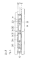
- Fig. 1 shows a rectangular LCD display element with a first, optically transparent cover 1 and a second optically transparent cover 2.
- the two cover plates 1 and 2 are the same width and the first cover is slightly longer, resulting in a contact edge 4.
- the edges of the two cover plates 1 and 2 define a left side edge 5, a right side edge 6, an upper side edge 7 and a lower side edge 8.
- a layer of liquid crystal 10 is arranged - see FIGS. 4 to 6 , By an adhesive edge 12, the two optically transparent cover plates. 1 and 2 spaced apart.
- the liquid crystal 10 is completely enclosed by the two cover disks 1 and 2 and the adhesive edge 12.
- a matrix-shaped electrode arrangement 14 which, by way of example, has five substantially strip-shaped row electrodes ZE1 to ZE5 and five, substantially strip-shaped, rectangular column electrodes SE1 to SE5.
- the column electrodes SE are arranged in a first plane 16 on the inside of the first cover plate 1 and have a first electrode end 18 and a second electrode end 19.
- spacer regions 20 are provided which electrically insulate the column electrodes SE1 to SE5 from each other.
- the row electrodes ZE1 to ZE5 are arranged in a second plane 22 on the inside of the second cover 2.
- the individual row electrodes ZE1 to ZE5 are electrically isolated from one another by separation regions 24.
- the crossover areas between row and column electrodes ZE and SE define with the liquid crystal 10 therebetween the individual pixels 26 of the LCD display element.
- the area of these pixels 26 defines a rectangular viewing area 28 - in Fig. 1 shown in dashed lines, in which information can be visually displayed.
- an LCD orientation layer 30 is disposed above the row or column electrodes ZE, SE.
- Both the row inlets Z1 to Z5 and the column inlets S1 to S5 are arranged in the first plane 16 on the inside of the first cover plate 1.
- the column leads Si contact the column electrodes SEi each at their first electrode end 18.
- the column leads Si are guided in the region of the lower side edge 8 under the adhesive edge 12 to the contact edge 4.
- the row feeders Z1 to Z4 are routed between the column electrodes SE in the space regions 20.
- the fifth line feed Z5 to the fifth line electrode ZE5 is guided in the region between the first column electrode SE1 and the adhesive edge 12. Alternatively, the fifth line feed Z5 may also be arranged below the adhesive edge 12.
- Both row and column electrodes ZE, SE and row and column leads S, Z are made of ITO.
- the individual, strip-shaped row electrodes ZEi each have a constriction 32, in which the adjacent row electrodes hineinerumblen 34 with finger-like pin.
- How out Fig. 2 can be seen, extend the individual line feeders Z1 to Z5 in the first level 16 on the Entire field of view 28.
- electrical contact elements 36-i are provided which displace the liquid crystal 10 from the first plane 16 to the second plane 22 and in the region of the first plane 16 a first contact surface 46 and in the region of second level 22 have a second contact surface 40.
- the first contact surface 46 establishes the electrical contact with the respective row supply line Zi and the second contact surface 40 establishes the electrical contact with the constriction 32 of the respective row electrode ZEi.
- the spacing regions 20 are widened in the region of the electrical contact elements 36, in which the column electrodes SE have semicircular recesses 42. In this way, remains around the first contact surfaces 46 of the contact elements 36 around a sufficient isolation distance. This safely prevents short circuits.
- the electrical contact elements 36 are electrically conductive only in the direction perpendicular to the cover plates 1, 2, but not in the transverse direction thereto. This is in Fig. 4 and Fig. 6 indicated by vertical lines 44. How this electrical conductivity is achieved in only one direction, will be described below with reference to FIGS. 7d to 7e oe Congresst.
- the first line feed Z1 for driving the first row electrode ZE1 between the fourth and the fifth column electrode SE4, SE5 is arranged.
- the second line feed Z2 for driving the second line electrode ZE3 is arranged in the region between the third and the fourth column electrode SE3, SE4.
- the third line feed Z3 for driving the third line electrode ZE3 is arranged in the region between the second and the third column electrode SE2, SE3.
- the fourth line feed Z4 for driving the fourth line electrode ZE4 is arranged in the region between the first and second column electrodes SE1, SE2.
- the fifth line feed Z5 for driving the fifth line electrode ZE5 runs to the right of the first column electrode SE1.
- adhesive elements 46 and 46-i are arranged in the crossover regions of spacer regions 20 and separation regions.
- the adhesive elements 46 displace the liquid crystal 10 and connect the two cover plates 1 and 2 with each other.
- the adhesive elements 46 extend in a straight line to the left and to the right and parallel to the line spanned by the contact elements 36. Thus, between 1% and 5% of the crossover areas of separation areas 24 and spacing areas 20 are provided with adhesive elements 46.
- the symmetrically arranged to the contact elements 36 adhesive elements 46 ensures that Even with temperature changes, the electrical contact surfaces 38, 40 of the contact elements 36 with the respective line feed Zi and the constriction 32 of the respective row electrode ZEi remain in contact and no detachment takes place.
- Fig. 4 shows a sectional view through the center of the distance region 20 between the second and third column electrode SE2, SE3 along the line A - A in Fig. 1
- Fig. 5 shows a sectional view along the center of the fourth column electrode SE4 and the associated fourth column lead S4 along the line B - B
- Fig. 6 shows a sectional view along the center of the third row electrode ZE3 along the line C - C in Fig. 1 ,
- FIGS. 7 and 8th FIG. 5 exemplarily shows true-to-scale embodiments of four immediately adjacent pixels 26-A, 26-B, 26-C and 26-D and 26-a, 26-b, 26c and 26-d, respectively.
- the pixels 26 have a rectangular basic shape.
- the separation regions 24 are approximately 0.05 mm wide and thus much thinner than the approximately 0.3 mm wide spacing regions 20 in which the line feed lines Z are guided.
- the width of the line feed lines Z is about 0.1 mm.
- the strip-shaped constrictions 32 of the row electrodes have a width of about 1 mm.
- the diameter of the adhesive elements 46 and the electrical contact elements 36 is about 0.3 mm.
- the individual pixels 26 have a width of 1.8 mm and a height of about 2.1 mm.
- FIGS. 7a to 7f show by way of example the electrical contact element 36-4 Fig. 1 , which connects the second row line Z2 to the second row electrode ZE2, in detail.
- Fig. 7a shows the position of the electrical contact element 36-4 in plan view of the first plane 16 with the second and third column electrodes SE2, SE3.
- Fig. 7b shows the position of the electrical contact element 36-4 in plan view of the second plane 22 with the third and second row electrode ZE3, ZE2.
- Fig. 7c shows a superposition of the FIGS. 7a and 7b.
- Fig. 7d shows the electrical contact element 36-4 Fig. 7c in magnification.
- Fig. 7e shows a section along the line A - A in Fig. 7d.
- Fig. 7f finally, it shows an enlarged section of the section Fig. 7e ,
- the electrical contact elements 36 are electrically conductive only in the direction perpendicular to the electrode assembly 14. This is achieved by a specific arrangement and configuration of electrically conductive particles 48 in the electrical contact elements 36.
- the distance d - see Fig. 7f - The insides of the two cover plates 1, 2 is about 5 up to 10 ⁇ m.
- the diameter of an electrical contact element 36 is in supervision about 0.3 mm - see Fig. 7d .
- the conductive particles 48, z. B. in the form of gold-coated plastic beads, have a mean diameter d x , which is slightly larger than the cell gap d (distance of the two cover discs 1,2). Ie.
- the mean diameter d x of the conductive particles 48 is between 10% and 20% greater than the distance d of the two cover disks 1, 2. Therefore, the conductive particles 48 between the two cover plates 1, 2 are clamped and compressed see Fig. 7f , so that the two electrical contact surfaces 38 and 40 result, which make the electrical contact with the row electrode ZE and the line feed Z. How out Fig. 7d can be seen, the single layer of electrically conductive particles 48 is statistically distributed over the cross-sectional area of the electrical contact elements 36 that results in a mean distance D between the individual particles 48, which is substantially greater than their diameter d x .
- the electrical contact elements 36 are electrically conductive in the direction perpendicular to the cover plates 1 and 2 and electrically non-conductive in the direction parallel to the two cover plates 1 and 2.
- 8a, 8b, 8c and 8d show in an analogous manner to the representation in the FIGS. 7a to 7d
- the adhesive member 46-3 between four pixels 26-a, 26b, 26-d and 26-c - see Fig. 1
- Fig. 8a shows the position of the adhesive member 46-3 in plan view of the first plane 16 with the fourth and fifth column electrodes SE4, SE5.
- Fig. 8b shows the position of the adhesive element 46-3 in plan view of the second plane 22 with the third and fourth row electrodes ZE3, ZE4.
- Fig. 8c shows a superposition of the Figures 8a and 8.
- Figure 8d shows adhesive element 46-3 Fig. 8c in magnification.
- the row electrode ZE in question and the associated column electrode SE For driving (ON state) or for non-control (OFF state) of a particular pixel P, the row electrode ZE in question and the associated column electrode SE with a sequence of row and column voltage pulses in the form of two successive square-wave voltage pulses U Z11 and U Z12 or U Z01 and U Z02 and U S11 and U S12 or U S01 and U S02 acted upon.
- the pixel P turns to the ON state when the resultant pixel voltage Up as the difference of the applied row and column voltage pulses is above the threshold voltage U threshold at which the liquid crystal 10 changes from the OFF state to the ON state.
- the threshold voltage U threshold at ⁇ 35 Vogt
- the pixel 26-A in Fig. 1 to the ON state and the pixel 26-C is turned to the OFF state the line voltage pulse train U Z11 and U Z12 , ie, 0 and 40 volts for the ON state, is applied to the row electrode Z3.
- Fig. 10 in an analogous way to Fig. 9 shown row and column voltage pulse trains, the unwanted switching to the intermediate state is easily prevented by the voltage pulse trains which are applied to row electrodes and column electrodes, are reversed. Ie.
- the row electrodes ZE are driven by the column voltage pulse trains and the column electrodes SE are driven by line voltage pulse trains according to the prior art.
- Fig. 10 shown.
- the threshold voltage U threshold of ⁇ 35 volts is clearly exceeded only for the resulting pixel voltage pulse sequence U P ⁇ 1 , U P ⁇ 2 , and the pixel in question clearly in the ON state.
- U P ⁇ 1, U P ⁇ 2, U P ⁇ 1, U P ⁇ 2 and U P ⁇ 1 U P ⁇ 2 threshold voltage U threshold of ⁇ 35 volts is significantly undershot, so that these pixel voltage pulse sequences representing all the OFF state of the respective pixel.
- U P ⁇ 2 threshold voltage U threshold of ⁇ 35 volts is significantly undershot, so that these pixel voltage pulse sequences representing all the OFF state of the respective pixel.
- For the control of individual pixels 26 results thus no difference to the state of the art. Ie. a certain pixel 26 is surely put in the ON or OFF state.
- the updating or description direction follows in the prior art Fig. 9 line by line, where all or selected lines can be described.
- the update or description direction is column by column due to the interchange of row and column voltages. Again, all or selected columns can be described.
- Individual LCD display elements according to the present invention can be connected to display panels in the same way as described with reference to FIGS. 9a, 9b and 10 in EP 1 962 129 A1 is described.
- By the shingled arrangement according to Fig. 10 in EP 1 962 129 A1 can be provided almost arbitrarily large scoreboards.
Landscapes
- Physics & Mathematics (AREA)
- Nonlinear Science (AREA)
- Mathematical Physics (AREA)
- Chemical & Material Sciences (AREA)
- Crystallography & Structural Chemistry (AREA)
- General Physics & Mathematics (AREA)
- Optics & Photonics (AREA)
- Liquid Crystal (AREA)
- Devices For Indicating Variable Information By Combining Individual Elements (AREA)
Abstract
Es wird ein LCD-Anzeigeelement, eine LCD-Anzeigetafel mit einer Mehrzahl solcher LCD-Anzeigeelemente sowie ein Verfahren zur Ansteuerung eines LCD-Anzeigeelements bzw. einer LCD-Anzeigetafel angegeben, wobei Übersprechen im Überkreuzungsbereich (X) zwischen Zeilenzuleitungen (Zi) und Zeilenelektroden (ZEi) vermieden wird. Dadurch, dass die elektrischen Zeilenzuleitungen in den Abstandsbereichen zwischen zwei Spaltenelektroden (Si) in der ersten Ebene sich unabhängig von der Position des elektrischen Kontaktelementes (36-i) über das gesamte Sichtfeld und die gesamte Länge der Spaltenelektroden erstrecken, kann der Bereich der Anzeige bzw. des Sichtfeldes verringert werden, der nicht gezielt beeinflusst werden kann. Durch dieses erfindungsgemäße Layout der Zeilenzuleitungen können die nicht gezielt beeinflussbaren Bereiche der Anzeige auf die elektrischen Kontaktelemente und die Kleberelemente (46-i) beschränkt werden. An den elektrischen Kontaktelementen und an den Kleberelementen erübrigt sich mangels Flüssigkristall eine gezielte Beeinflussung. Durch das erfindungsgemäße Layout liegt der Flüssigkristall in den Abstandsbereichen nur zwischen Zeilenzuleitungen und den durch die Trennbereiche voneinander getrennten Zeilenelektroden. Dadurch kann im Normalbetrieb der Anzeige die auf den Flüssigkristall wirkende resultierende Spannung immer unter der Schwellspannung gehalten werden. Zur Initialisierung der Anzeige kann der Flüssigkristall in den Abstandsbereichen gezielt orientiert werden.An LCD display element, an LCD display panel having a plurality of such LCD display elements and a method for driving an LCD display element or LCD display panel are provided, wherein crosstalk in the crossover area (X) between row leads (Zi) and row electrodes ( ZEi) is avoided. The fact that the electrical line feed lines in the distance regions between two column electrodes (Si) in the first plane extend independently of the position of the electrical contact element (36-i) over the entire field of view and the entire length of the column electrodes, the range of the display or . of the field of view can be reduced, which can not be specifically influenced. As a result of this layout according to the invention of the row feeders, the areas of the display which can not be specifically influenced can be limited to the electrical contact elements and the adhesive elements (46-i). At the electrical contact elements and the adhesive elements is unnecessary lack of liquid crystal targeted influence. As a result of the layout according to the invention, the liquid crystal in the distance regions lies only between line feed lines and the line electrodes which are separated from one another by the separating regions. As a result, during normal operation of the display, the resulting voltage acting on the liquid crystal can always be kept below the threshold voltage. To initialize the display, the liquid crystal can be selectively oriented in the spacing regions.
Description
Die vorliegende Erfindung betrifft ein LCD-Anzeigeelement nach dem Oberbegriff des Anspruchs 1 eine LCD-Anzeigetafel mit einer Mehrzahl solcher LCD-Anzeigeelemente nach Anspruch 27 sowie ein Verfahren zur Ansteuerung eines LCD-Anzeigeelements bzw. einer LCD-Anzeigetafel nach Anspruch 28.The present invention relates to an LCD display element according to the preamble of
Derartige LCD-Anzeigeelemente umfassen einen Flüssigkristall, der zwischen zwei optisch durchlässigen Abdeckscheiben mittels eines Kleberandes eingeschlossen ist. Auf der Innenseite der beiden Abdeckscheiben ist eine Elektrodenanordnung in Matrixform mit Zeilen und Spaltenelektroden angeordnet, die in der Regel streifenförmig sind. Die streifenförmigen Zeilenelektroden sind durch Trennungsbereiche voneinander getrennt und die streifenförmigen Spaltenelektroden sind durch Abstandsbereiche voneinander getrennt. Die Überkreuzungsbereiche zwischen Zeilen- und Spaltenelektroden legen mit dem Flüssigkristall dazwischen die einzelnen Pixel des LCD-Anzeigeelements fest. Das Elektrodenmaterial besteht üblicherweise aus ITO.Such LCD display elements comprise a liquid crystal which is enclosed between two optically transmissive cover plates by means of an adhesive edge. On the inside of the two cover plates, an electrode arrangement is arranged in matrix form with rows and column electrodes, which are generally strip-shaped. The stripe-shaped row electrodes are separated from each other by separation areas, and the stripe-shaped column electrodes are separated from each other by pitch areas. The crossover areas between row and column electrodes define the individual pixels of the LCD display element with the liquid crystal therebetween. The electrode material is usually made of ITO.
Aus der
Aus der
Ausgehend von der
Die Lösung dieser Aufgabe erfolgt durch die Merkmale der Ansprüche 1 bzw. 27 bzw. 28.The solution of this object is achieved by the features of
Dadurch, dass die elektrischen Zeilenzuleitungen in den Abstandsbereichen zwischen zwei Spaltenelektroden in der ersten Ebene sich unabhängig von der Position des elektrischen Kontaktelementes über das gesamte Sichtfeld und die gesamte Länge der Spaltenelektroden erstrecken, kann der Bereich der Anzeige bzw. des Sichtfeldes verringert werden, der nicht gezielt beeinflusst werden kann. Durch dieses erfindungsgemäße Layout der Zeilenzuleitungen können die nicht gezielt beeinflussbaren Bereiche der Anzeige auf die elektrischen Kontaktelemente und die Kleberelemente beschränkt werden. An den elektrischen Kontaktelementen und an den Kleberelementen erübrigt sich mangels Flüssigkristall eine gezielte Beeinflussung. Durch das erfindungsgemäße Layout liegt der Flüssigkristall in den Abstandsbereichen nur zwischen Zeilenzuleitungen und den durch die Trennbereiche voneinander getrennten Zeilenelektroden, Dadurch kann im Normalbetrieb der Anzeige die auf den Flüssigkristall wirkende resultierende Spannung immer unter der Schwellspannung gehalten werden. Zur Initialisierung der Anzeige kann der Flüssigkristall in den Abstandsbereichen gezielt orientiert werden.The fact that the line electrical leads in the pitch regions between two column electrodes in the first plane extend independently of the position of the electrical contact element over the entire field of view and the entire length of the column electrodes can reduce the range of the display or field of view which does not can be specifically influenced. As a result of this layout according to the invention of the row feeders, the areas of the display which can not be specifically influenced can be limited to the electrical contact elements and the adhesive elements. At the electrical contact elements and the adhesive elements is unnecessary lack of liquid crystal targeted influence. As a result of the layout according to the invention, the liquid crystal in the distance ranges lies only between row inlets and the row electrodes which are separated from one another by the separation areas. Thus, during normal operation of the display, the resulting voltage acting on the liquid crystal can always be kept below the threshold voltage. For initialization the display, the liquid crystal can be targeted in the distance ranges.
Zeilenzuleitungen werden nicht nur in den Abstandsbereichen zwischen zwei Spaltenelektroden geführt, sondern auch entlang der Außenseite der beiden äußersten Spaltenelektroden, Nach der vorteilhaften Ausgestaltung der Erfindung nach Anspruch 2 erstrecken sich auch diese Zeilenzuleitungen über das gesamte Sichtfeld. Hierdurch ergibt sich ein einheitliches optisches Erscheinungsbild der Anzeige.
Durch die vorteilhafte Ausgestaltung der Erfindung nach Anspruch 3 ergeben sich kurze Spaltenzuleitungen.Line feeders are not only routed in the pitch regions between two column electrodes, but also along the outside of the two outermost column electrodes. According to the advantageous embodiment of the invention according to
Due to the advantageous embodiment of the invention according to claim 3, short column leads arise.
Durch die vorteilhafte Ausgestaltung der Erfindung nach Anspruch 5 bis 7 wird die im Sichtbereich liegende Fläche in den Abstandsbereichen zwischen den Spaltenelektroden, die nicht gezielt angesteuert wird, weiter verkleinert.Due to the advantageous embodiment of the invention according to
Durch die Ausgestaltung nach Anspruch 8 wird sichergestellt, dass es im Bereich der Kontaktelemente nicht zu Kurzschlüssen kommt.The embodiment according to
Für den Fall, dass die Zahl z der Zeilenelektroden kleiner ist als die Zahl s der Spaltenelektroden ist nach Anspruch 9 höchstens eine Zeilenzuleitung zwischen zwei Spaltenelektroden geführt. Für den Fall, das die Zahl z der Zeilenelektroden größer oder gleich der Zahl s der Spaltenelektroden ist, ist nach Anspruch 10 zwischen allen Spaltenelektroden wenigstens eine Zeilenzuleitung geführt. In beiden Fällen wird erreicht, dass die Abstandsbereiche möglichst schmal ausgeführt werden können.In the event that the number z of the row electrodes is smaller than the number s of the column electrodes, at most one row lead is guided between two column electrodes according to claim 9. In the event that the number z of the row electrodes is greater than or equal to the number s of the column electrodes, at least one row lead is passed between all column electrodes according to
Bei der vorteilhaften Ausgestaltung der Erfindung nach Anspruch 11 ist zwischen allen Spaltenelektroden jeweils eine Zeilenzuleitung vorgesehen, auch wenn aufgrund der geringeren Anzahl von Zeilenelektroden gar keine Zeilenzuleitung zwischen allen Spaltenelektroden notwendig wäre. Durch die elektrisch kontaktierenden Zeilenzuleitungen und durch die Dummy-Zeilenzuleitungen werden jedoch die Beeinflussbarkeit aller Abstandsbereiche und ein gleichförmiger optischer Eindruck der Anzeige im Sichtbereich gewährleistet.In the advantageous embodiment of the invention according to
Gemäß der vorteilhaften Ausgestaltung der Erfindung nach Anspruch 12 werden sowohl die Zeilen als auch die Spaltenzuleitungen an einer gemeinsamen geraden LCD-Kante bzw. Seitenkante durch den Kleberand nach außen geführt. Hierdurch können die LCD-Elemente an den verbleibenden Seitenkanten nebeneinander zu einer LCD-Anzeigetafel angeordnet werden.According to the advantageous embodiment of the invention according to
Durch die vorteilhafte Ausgestaltung der Erfindung nach Anspruch 13 ergibt sich eine Flüssigkristall-Zelle bzw. eine LCD-Anzeigeelement mit einem konstanten Abstand der beiden Abdeckscheiben, da die beiden Abdeckscheiben nicht nur im Bereich des Kleberands, sondern auch im Bereich der Klebepunkte miteinander verbunden sind.Due to the advantageous embodiment of the invention according to claim 13 results in a liquid crystal cell or an LCD display element with a constant distance between the two cover plates, since the two cover plates are connected to each other not only in the region of the adhesive edge, but also in the adhesive dots.
Durch die vorteilhafte Ausgestaltung der Erfindung nach Anspruch 14 wird sichergestellt, dass auch bei Temperaturschwankungen der elektrische Kontakt zwischen Zeilenzuleitungen, elektrischen Kontaktelementen und Zeilenelektroden erhalten bleibt.The advantageous embodiment of the invention according to
Die in Anspruch 15 genannten Werte ergeben zufriedenstellende optische Eindrücke des LCD-Anzeigelements.The values mentioned in claim 15 give satisfactory visual impressions of the LCD display element.
Durch die vorteilhafte Ausgestaltung der Erfindung nach Anspruch 16 können Kleberrand und Kleberelemente in einem Arbeitsgang auf eine der Abdeckscheiben aufgebracht werden. Die Kleberelemente und/oder die elektrischen Kontaktelemente können auch mit dem Kleberand verfliesen.Due to the advantageous embodiment of the invention according to claim 16 adhesive edge and adhesive elements can be applied in one operation on one of the cover plates. The adhesive elements and / or the electrical contact elements can also tiling with the adhesive edge.
Durch die vorteilhafte Ausgestaltung der Erfindung nach Anspruch 17 und 18 vereinfacht sich die Herstellung der elektrischen Kontaktelemente.Due to the advantageous embodiment of the invention according to
Durch die vorteilhafte Ausgestaltung der Erfindung nach Anspruch 19 wird auf einfache Weise ein elektrischer Leiter bereitgestellt, der nur in einer Richtung, nämlich in senkrechter Richtung zu der ersten und zweiten Ebene elektrisch leitend ist, nicht jedoch in Querrichtung hierzu, d. h. in Richtung parallel zu der ersten und zweiten Ebene. Hierdurch wird es möglich die elektrischen Kontaktelemente vergleichsweise groß auszubilden, da ein Kurzschluss zwischen zwei benachbarten Zeilenelektroden aufgrund der fehlenden elektrischen Leitfähigkeit in Querrichtung nicht möglich ist. Da der mittlere Durchmesser der leitfähigen Partikel etwas größer ist als der Abstand der beiden Abdeckscheiben, werden die leitfähigen Partikel zwischen den beiden Abdeckscheiben eingeklemmt, so dass sich ein guter elektrischer Kontakt zu der jeweiligen Zeilenelektrode und der zugehörigen Zeilenzuleitung ergibt. Es liegt also eine einlagige Schicht aus leitfähigen Partikeln vor. Da die elektrisch leitfähigen Partikel mit Abstand zueinander angeordnet sind, sind die elektrischen Kontaktelemente in Querrichtung bzw. in Richtung parallel zu der ersten und zweiten Ebene nicht elektrische leitend. Diese gewünschte Anordnung der leitfähigen Partikel wird durch eine entsprechende Konzentration und durch entsprechende statistische Verteilung der leitfähigen Partikel in dem Klebermaterial der elektrischen Kontaktelemente oder auf der Flüssigkristall-Orientierungsschicht im Bereich der elektrischen Kontaktelemente erzielt.Due to the advantageous embodiment of the invention according to
Dadurch, dass die Spannungsimpulse für Zeilen und Spalten so gewählt werden, dass die beiden Ungleichungen ![]()
und ![]()
erfüllt sind - Anspruch 22, wird erreicht, dass während der gesamten Sequenz von Zeilen- und Spaltenspannungsimpulsen die Mindestspannung für den Zustand EIN im Überkreuzungsbereich zwischen Zeilenzuleitungen und Zeilenelektroden nicht erreicht wird.Because the voltage pulses for rows and columns are chosen so that the two inequalities ![]()
and ![]()
are satisfied, it is achieved that during the entire sequence of row and column voltage pulses, the minimum voltage for the ON state in the crossing region between line feeders and line electrodes is not achieved.
Die Ungleichungen (1) und (2) werden am einfachsten dadurch erfüllt, dass im Vergleich zu einem herkömmlichen Ansteuerungsschema für ein Passiv-Matrix-Flüssigkristall-Anzeigeelement die Zeilenspannungsimpulse mit den Spaltenspannungsimpulsen vertauscht werden - Anspruch 27.The inequalities (1) and (2) are most easily satisfied by interchanging the line voltage pulses with the column voltage pulses as compared with a conventional drive scheme for a passive matrix liquid crystal display element.
Durch die Erfüllung der Ungleichungen in den Unteransprüchen 23 bis 26 werden bevorzugte Relationen zwischen den einzelnen Zeilen- und Spaltenspannungsimpulsen angegeben, mit denen ein Ansteuern unerwünschter Bereiche sicher ausgeschlossen ist.By satisfying the inequalities in the dependent claims 23 to 26, preferred relations between the individual row and column voltage pulses are specified, with which a triggering of undesired areas is reliably excluded.
Die übrigen Unteransprüche beziehen sich auf weitere vorteilhafte Ausgestaltungen der Erfindung.The remaining subclaims relate to further advantageous embodiments of the invention.
Weitere Einzelheiten, Merkmale und Vorteile der Erfindung ergeben sich aus der nachfolgenden Beschreibung einer bevorzugten Ausführungsform anhand der Zeichnung.Further details, features and advantages of the invention will become apparent from the following description of a preferred embodiment with reference to the drawing.
Es zeigt:
-
Fig. 1 eine schematische Darstellung einer beispielhaften Ausführungsform der Erfindung; -
Fig. 2 das Layout der Spaltenelektroden der Ausführungsform nachFig. 1 ; -
Fig. 3 das Layout der Zeilenelektroden der Ausführungsform nachFig. 1 ; -
Fig. 4 eine Schnittdarstellung der Ausführungsform nachFig. 1 entlang der Linie A-A; -
Fig. 5 eine Schnittdarstellung der Ausführungsform nachFig. 1 entlang der Linie B-B; -
Fig. 6 eine Schnittdarstellung der Ausführungsform nachFig. 1 entlang der Linie C-C; -
Fig. 7a, 7b, 7c, 7d, 7e und 7f verschiedene Detaildarstellungen einer beispielhaften Ausgestaltung der elektrische Kontaktelemente; -
Fig. 8a und 8b eine Detaildarstellung eines Kleberelements; -
Fig. 9 Signalformen und Signalgrößen eines mittels Multiplex angesteuerten LCD-Anzeigeelements nach dem Stand der Technik gemäß derEP 1 962 129 A1 -
Fig. 10 Signalformen und Signalgrößen eines mittels Multiplex angesteuerten LCD-Anzeigeelements gemäß der vorliegenden Erfindung.
-
Fig. 1 a schematic representation of an exemplary embodiment of the invention; -
Fig. 2 the layout of the column electrodes of the embodiment according toFig. 1 ; -
Fig. 3 the layout of the row electrodes of the embodiment according toFig. 1 ; -
Fig. 4 a sectional view of the embodiment according toFig. 1 along the line AA; -
Fig. 5 a sectional view of the embodiment according toFig. 1 along the line BB; -
Fig. 6 a sectional view of the embodiment according toFig. 1 along the line CC; -
Fig. 7a, 7b, 7c, 7d, 7e and 7f various detailed representations of an exemplary embodiment of the electrical contact elements; -
Fig. 8a and 8b a detailed view of an adhesive element; -
Fig. 9 Waveforms and Signal Sizes of a Prior Art Multiplexed LCD Display Element According to thePrior Art EP 1 962 129 A1 -
Fig. 10 Waveforms and signal quantities of a multiplex driven LCD display element according to the present invention.
Die
Innerhalb des Kleberands 12 ist eine matrixförmige Elektrodenanordnung 14 vorgesehen, die beispielhaft fünf, im Wesentlichen streifenförmige Zeilenelektroden ZE1 bis ZE5 und fünf, im Wesentlichen streifenförmige, rechteckige Spaltenelektroden SE1 bis SE5 aufweist. Wie aus
Die Ansteuerung der Zeilen- bzw. Spaltenelektroden ZE bzw. SE erfolgt über Zeilenzuleitungen Z1 bis Z5 bzw. über Spaltenzuleitungen S1 bis S5. Sowohl die Zeilenzuleitungen Z1 bis Z5 als auch die Spaltenzuleitungen S1 bis S5 sind in der ersten Ebene 16 auf der Innenseite der ersten Abdeckscheibe 1 angeordnet. Die Spaltenzuleitungen Si kontaktieren die Spaltenelektroden SEi jeweils an deren erstem Elektrodenende 18. Die Spaltenzuleitungen Si werden im Bereich der unteren Seitenkante 8 unter dem Kleberand 12 zu dem Kontaktrand 4 geführt. Die Zeilenzuleitungen Z1 bis Z4 werden zwischen den Spaltenelektroden SE in dem Abstandsbereichen 20 geführt. Die fünfte Zeilenzuleitung Z5 zur fünften Zeilenelektrode ZE5 wird im Bereich zwischen erster Spaltenelektrode SE1 und dem Kleberand 12 geführt. Alternativ kann die fünfte Zeilenzuleitung Z5 auch unter dem Kleberand 12 angeordnet sein. Sowohl Zeilen-und Spaltenelektroden ZE, SE als auch Zeilen- und Spaltenzuleitungen S, Z bestehen aus ITO.The control of the row or column electrodes ZE or SE via line inlets Z1 to Z5 or column supply lines S1 to S5. Both the row inlets Z1 to Z5 and the column inlets S1 to S5 are arranged in the
Wie aus
Wie aus
Wie aus
Symmetrisch zu und in unmittelbarer Nachbarschaft zu den elektrischen Kontaktelementen 36 sind in den Überkreuzungsbereichen von Abstandsbereichen 20 und Trennungsbereichen 24 Kleberelemente 46 bzw. 46-i angeordnet. Die Kleberelemente 46 verdrängen den Flüssigkristall 10 und verbinden die beiden Abdeckscheiben 1 und 2 miteinander. Die Kleberelemente 46 erstrecken sich in gerader Linie links und rechts und parallel zu der von den Kontaktelementen 36 aufgespannten Geraden. Damit sind zwischen 1 % und 5% der Überkreuzungsbereichen von Trennungsbereichen 24 und Abstandsbereichen 20 mit Kleberelementen 46 versehen. Durch die symmetrisch zu den Kontaktelementen 36 angeordneten Kleberelemente 46 wird gewährleistet, dass auch bei Temperaturänderungen die elektrischen Kontaktflächen 38, 40 der Kontaktelemente 36 mit der jeweiligen Zeilenzuleitung Zi und der Einschnürung 32 der jeweiligen Zeilenelektrode ZEi in Kontakt bleiben und keine Ablösung erfolgt.Symmetrically to and in the immediate vicinity of the
Wie vorstehend bereits erläutert, zeigt
Die Darstellung der beispielhaften Ausführungsform der Erfindung in den
Wie bereits bei der Beschreibung der
![]()
![]()
![]()
![]()
die vier in ![]()
und ![]()
![]()
und ![]()
![]()
und ![]()
![]()
und ![]()
![]()
![]()
![]()
![]()
the four in ![]()
and ![]()
![]()
and ![]()
![]()
and ![]()
![]()
and ![]()
Damit wird nur für die resultierende Pixelspannungsimpulsfolge UPα1, UPα2, die Schwellenspannung USchwelle von ±35 Volt deutlich überschritten und das fragliche Pixel in den EIN-Zustand versetzt. Bei den übrigen Pixelspannungsimpulsfolgen UPβ1, UPβ2, UPγ1, UPγ2 und UPδ1, UPδ2 wird Schwellenspannung USchwelle von ±35 Volt deutlich unterschritten, so dass diese Pixelspannungsimpulsfolgen alle den AUS-Zustand des jeweiligen Pixels darstellen.Thus, only for the resulting pixel voltage pulse sequence U Pα1 , U Pα2 , the threshold voltage U threshold of ± 35 volts is clearly exceeded and put the pixel in question in the ON state. For the remaining pixel voltage pulse trains U Pβ1, U Pβ2, U Pγ1, U Pγ2 and U Pδ1, U Pδ2 threshold voltage U threshold of ± 35 volts is significantly undershot, so that these pixel voltage pulse sequences representing all the OFF state of the respective pixel.
Wird mit einem Multiplex-Ansteuerungsverfahren nach dem Stand der Technik gemäß der ![]()
und ![]()
beaufschlagt, d. h. der Flüssigkristall 10 im Bereich X wird mit der Schwellenspannung USchwell angesteuert und liegt somit in einem Zwischenzustand zwischen EIN und AUS.Used with a prior art multiplex driving method according to the ![]()
and ![]()
acted upon, ie, the
Dieses ungewollte Erzeugen des Zwischenzustandes zwischen EIN und AUS im Bereich X in den Trennungsbereichen 20 zwischen Zeilenzuleitungen Z und Zeilenelektroden ZE wird durch die Wahl der Zeilen- und Spaltenspannungsimpulsfolgen gemäß der vorliegenden Erfindung vermieden. ![]()
![]()
![]()
und ![]()
![]()
und ![]()
![]()
und ![]()
![]()
![]()
![]()
and ![]()
![]()
and ![]()
![]()
and ![]()
Damit wird nur für die resultierende Pixelspannungsimpulsfolge UPα1, UPα2, die Schwellenspannung USchwelle von ±35 Volt deutlich überschritten und das fragliche Pixel eindeutig in den EIN-Zustand versetzt. Bei den übrigen Pixelspannungsimpulsfolgen UPβ1, UPβ2, UPγ1, UPγ2 und UPδ1, UPδ2 wird Schwellenspannung USchwelle von ±35 Volt deutlich unterschritten, so dass diese Pixelspannungsimpulsfolgen alle den AUS-Zustand des jeweiligen Pixels darstellen. Für die Ansteuerung einzelner Pixel 26 ergibt sich somit kein Unterschied zum Stand der Technik. D. h. ein bestimmtes Pixel 26 wird sicher in den EIN- oder AUS-Zustand versetzt.Thus, the threshold voltage U threshold of ± 35 volts is clearly exceeded only for the resulting pixel voltage pulse sequence U Pα1 , U Pα2 , and the pixel in question clearly in the ON state. For the remaining pixel voltage pulse trains U Pβ1, U Pβ2, U Pγ1, U Pγ2 and U Pδ1, U Pδ2 threshold voltage U threshold of ± 35 volts is significantly undershot, so that these pixel voltage pulse sequences representing all the OFF state of the respective pixel. For the control of
Das beim Stand der Technik nach ![]()
und ![]()
beaufschlagt, d. h. der Flüssigkristall 10 im Bereich X wird sicher in den AUS-Zustand geschaltet. Übersprechen bzw. das Erzeugen eines ungewollten Zwischenzustandes zwischen Zeilenelektroden ZE und Zeilenzuleitungen Z in den Trennungsbereichen 20 wird sicher vermieden.The in the prior art after ![]()
and ![]()
is applied, that is, the
Die Update- bzw. Beschreibrichtung verläuft im Stand der Technik nach
Einzelne LCD-Anzeigeelemente gemäß der vorliegenden Erfindung lassen sich in gleicher Weise zu Anzeigetafeln verbinden, wie dies anhand der
- ZE1 bis ZE5ZE1 to ZE5
- Zeilenelektrodenrow electrodes
- SE1 bis SE5SE1 to SE5
- Spaltenelektrodencolumn electrodes
- Z1 bis Z5Z1 to Z5
- Zeilenzuleitungenrow leads
- S1 bis S5S1 to S5
- Spaltenzuleitungencolumn leads
- 11
- erste Abdeckscheibefirst cover
- 22
- zweite Abdeckscheibesecond cover
- 44
- KontaktrandContact edge
- 55
- linke Seitenkanteleft side edge
- 66
- rechte Seitenkanteright side edge
- 77
- obere Seitenkanteupper side edge
- 88th
- untere Seitenkantelower side edge
- 1010
- Flüssigkristallliquid crystal
- 1212
- Kleberandadhesive edge
- 1414
- Elektrodenanordnungelectrode assembly
- 1616
- erste Ebenefirst floor
- 1818
- erstes Elektrodenendefirst end of the electrode
- 1919
- zweites Elektrodenendesecond electrode end
- 2020
- Abstandsbereichedistance ranges
- 2222
- zweite Ebenesecond level
- 2424
- Trennungsbereicheseparation areas
- 2626
- Pixelpixel
- 2828
- Sichtfeldfield of view
- 3030
- LCD-OrientierungsschichtLCD alignment layer
- 3232
- Einschnürung der ZEConstriction of the ZE
- 3434
- fingerartigen Zapfenfinger-like cones
- 3636
- elektrische Kontaktelementeelectrical contact elements
- 3838
- erste Kontaktfläche von 36first contact area of 36
- 4040
- zweite Kontaktfläche von 36second contact area of 36
- 4242
- Ausnehmung in SERecess in SE
- 4444
- senkrechte Striche in 36vertical lines in 36
- 4646
- Kleberelementeadhesive elements
- 4848
- leitfähige Partikel in 36conductive particles in 36
Claims (28)
dadurch gekennzeichnet,
dass diejenigen elektrischen Zeilenzuleitungen (Z), die im Abstandsbereich (20) zwischen zwei Spaltenelektroden (SE) verlaufen, sich quer über die Projektion aller Zeilenelektroden (ZE) auf die erste Ebene (16) erstrecken.
characterized,
in that those electrical line feed lines (Z) which run in the distance region (20) between two column electrodes (SE) extend across the projection of all line electrodes (ZE) onto the first plane (16). extend.
dadurch gekennzeichnet,
dass die z Zeilenelektroden (ZE) und die s Spaltenelektroden (SE) jeweils ein erstes und ein zweites Elektrodenende (18, 19) aufweisen und
dass die Spaltenzuleitungen (S) die Spaltenelektroden (SE) an den ersten Elektrodenenden (18) kontaktieren.LCD display element according to one of the preceding claims,
characterized,
that the z row electrodes (ZE) and the s column electrodes (SE) each have a first and a second electrode end (18, 19) and
in that the column feed lines (S) make contact with the column electrodes (SE) at the first electrode ends (18).
dadurch gekennzeichnet,
characterized,
dass jede Zeilenelektroden (ZE) eine Einschnürungen (32) aufweist, und
dass das jeweilige elektrische Kontaktelement (36) diese Einschnürung (32) kontaktiert.LCD display element according to one of the preceding claims, characterized
that each row electrodes (ZE) has a constriction (32), and
that the respective electrical contact element (36) contacts this constriction (32).
dadurch gekennzeichnet, dass die Spaltenelektroden (SE) in der ersten Ebene (16) im Bereich um die ersten Kontaktflächen (38) Ausnehmungen (42) aufweisen, so dass die Abstandsbereiche (20) in diesem Bereich verbreitert sind.LCD display element according to one of the preceding claims,
characterized in that the column electrodes (SE) in the first plane (16) in the region around the first contact surfaces (38) recesses (42), so that the spacer regions (20) are widened in this area.
dadurch gekennzeichnet, dass für z < s zwischen zwei benachbarten Spaltenelektroden (SE) höchstens eine der z Zeilenzuleitungen (Z) geführt ist.LCD display element according to one of the preceding claims,
characterized in that for z <s between two adjacent column electrodes (SE) at most one of z line feeders (Z) is guided.
dadurch gekennzeichnet, dass das LCD-Anzeigelement wenigstens eine gerade LCD-Kante (5, 6, 7, 8) aufweist und dass die Zeilen- und die Spaltenzuleitungen (Z, S) an dieser geraden LCD-Kante (8) unter dem Kleberand (12) nach außen geführt sind.LCD display element according to one of the preceding claims,
characterized in that the LCD display element has at least one straight LCD edge (5, 6, 7, 8) and that the row and the column feed lines (Z, S) at this straight LCD edge (8) under the adhesive edge ( 12) are guided to the outside.
dadurch gekennzeichnet, dass an Überkreuzungsbereichen der Abstandsbereiche (20) mit den Trennungsbereichen (24) Kleberelemente (46) angeordnet sind.LCD display element according to one of the preceding claims,
characterized in that at crossover regions of the spacer regions (20) with the separation regions (24) adhesive elements (46) are arranged.
dass auf den Innenseiten der beiden Abdeckscheiben (1, 2) eine Flüssigkristall-Orientierungsschicht (30) vorgesehen ist, und
dass die elektrischen Kontaktelemente (36) durch gezieltes Aufbringen von zusätzlichem Orientierungsschichtmaterial mit elektrisch leitfähigen Partikeln (48) auf die Flüssigkristall-Orientierungsschicht (30) bereitgestellt sind.LCD display element according to one of the preceding claims 1 to 15, characterized
in that a liquid crystal orientation layer (30) is provided on the insides of the two cover disks (1, 2), and
in that the electrical contact elements (36) are formed by selectively applying additional orientation layer material with electrically conductive Particles (48) are provided on the liquid crystal alignment layer (30).
eine Treibereinrichtung zur Ansteuerung der einzelnen Pixel durch Beaufschlagung der Spaltenelektroden (SE) mit einer ersten Sequenz von Spaltenspannungspulsen US0i mit i ∈ {1 .. n} mit n ≥ 2 für den Zustand AUS und durch Beaufschlagung mit einer zweiten Sequenz von Spaltenspannungsimpulsen US1i mit i ∈ {1 .. n} mit n ≥ 2 für den Zustand EIN, und
durch Beaufschlagung der Zeilenelektroden (ZE) mit einer ersten Sequenz von Zeilenspannungsimpulsen UZ0i mit i ∈ {1 .. n} mit n ≥ 2 für den Zustand AUS und durch Beaufschlagung mit einer zweiten Sequenz von Zeilenspannungsimpulsen UZ1i mit i ∈ {1 .. n} mit n ≥ 2 für den Zustand EIN.LCD display element according to one of the preceding claims, characterized by
a driver device for driving the individual pixels by applying the column electrodes (SE) with a first sequence of column voltage pulses U S0i with i ∈ {1 .. n} with n ≥ 2 for the state OFF and by applying a second sequence of column voltage pulses U S1i with i ∈ {1 .. n} with n ≥ 2 for the state ON, and
by applying the line electrodes (ZE) with a first sequence of line voltage pulses U Z0i with i ∈ {1 .. n} with n ≥ 2 for the state OFF and by applying a second sequence of line voltage pulses U Z1i with i ∈ {1 .. n} with n ≥ 2 for the ON state.
und
wobei US1max der maximale Spaltenspannungsimpuls aus der zweiten Sequenz von Spaltenspannungsimpulsen US1i ist,
wobei US0min der minimale Spaltenspannungsimpuls aus der ersten Sequenz von Spaltenspannungsimpulsen US0i ist,
wobei UZ1max der maximale Zeilenspannungsimpuls aus der zweiten Sequenz von Zeilenspannungsimpulsen UZ1i ist, und
wobei UZ0min der minimale Zeilenspannungsimpuls aus der ersten Sequenz von Zeilenspannungsimpulsen UZ0i ist.LCD display element according to Claim 21, characterized in that the voltage pulses (U Z0i ; U Z1i ; U S0i ; U S1i ) generated by the driver device satisfy the following inequalities (1) and (2):
and
where U S1max is the maximum column voltage pulse from the second sequence of column voltage pulses U S1i ,
where U S0min is the minimum column voltage pulse from the first sequence of column voltage pulses U S0i ,
where U Z1max is the maximum row voltage pulse from the second sequence of row voltage pulses U Z1i , and
where U Z0min is the minimum row voltage pulse from the first sequence of row voltage pulses U Z0i .
und
and
und
and
und
and
und
and
Applications Claiming Priority (1)
| Application Number | Priority Date | Filing Date | Title |
|---|---|---|---|
| DE102009032273A DE102009032273A1 (en) | 2009-07-08 | 2009-07-08 | LCD display element and LCD display panel |
Publications (2)
| Publication Number | Publication Date |
|---|---|
| EP2284603A1 true EP2284603A1 (en) | 2011-02-16 |
| EP2284603B1 EP2284603B1 (en) | 2017-05-17 |
Family
ID=42542792
Family Applications (1)
| Application Number | Title | Priority Date | Filing Date |
|---|---|---|---|
| EP10168901.6A Not-in-force EP2284603B1 (en) | 2009-07-08 | 2010-07-08 | LCD display element |
Country Status (4)
| Country | Link |
|---|---|
| US (1) | US8587570B2 (en) |
| EP (1) | EP2284603B1 (en) |
| CA (1) | CA2709179A1 (en) |
| DE (1) | DE102009032273A1 (en) |
Families Citing this family (5)
| Publication number | Priority date | Publication date | Assignee | Title |
|---|---|---|---|---|
| TWI449013B (en) * | 2012-05-22 | 2014-08-11 | Au Optronics Corp | Display apparatus and operation method thereof |
| JP6672152B2 (en) * | 2013-09-30 | 2020-03-25 | エルジー・ケム・リミテッド | Substrate for organic electronic device and method for producing the same |
| US9785032B2 (en) | 2013-11-12 | 2017-10-10 | E Ink Holdings Inc. | Active device array substrate and display panel |
| TWI505010B (en) * | 2013-11-12 | 2015-10-21 | E Ink Holdings Inc | Active device array substrate |
| KR102422576B1 (en) | 2015-10-14 | 2022-07-21 | 삼성디스플레이 주식회사 | Liquid crystal display device |
Citations (4)
| Publication number | Priority date | Publication date | Assignee | Title |
|---|---|---|---|---|
| JP2001311955A (en) * | 2000-02-24 | 2001-11-09 | Seiko Epson Corp | Liquid crystal device and electronic equipment using the same |
| US20070139299A1 (en) | 2003-07-02 | 2007-06-21 | Kent Display Incorporated | Stacked display with shared electrode addressing |
| EP1962129A1 (en) | 2007-02-26 | 2008-08-27 | AEG Gesellschaft für moderne Informationssysteme mbH | Passive-matrix LCD element and tiled LCD panel with a plurality of such elements |
| US20080291187A1 (en) | 2006-03-30 | 2008-11-27 | Fujitsu Limited | Drive method and display device of display element |
Family Cites Families (10)
| Publication number | Priority date | Publication date | Assignee | Title |
|---|---|---|---|---|
| DE2058104C2 (en) | 1970-11-26 | 1987-01-02 | Licentia Patent-Verwaltungs-Gmbh, 6000 Frankfurt | Liq. crystal seven-segment display - has conductive spacers connecting outer metallisation regions on base layer to upper electrode |
| JPH0545667A (en) | 1991-08-20 | 1993-02-26 | Hitachi Ltd | Dot matrix type display device |
| DE4310112A1 (en) | 1993-03-27 | 1994-09-29 | Licentia Gmbh | Liquid-crystal display device |
| JP3595153B2 (en) * | 1998-03-03 | 2004-12-02 | 株式会社 日立ディスプレイズ | Liquid crystal display device and video signal line driving means |
| JP3708770B2 (en) | 1999-12-24 | 2005-10-19 | セイコーエプソン株式会社 | Manufacturing method of liquid crystal device |
| ATE310299T1 (en) | 2000-02-24 | 2005-12-15 | Aeg Ges Moderne Inf Sys Mbh | LCD PIXEL MATRIX ELEMENT AND GRAPHICS ENABLED LCD DISPLAY PANEL HAVING A PLURALITY OF SUCH LCD PIXEL MATRIX ELEMENTS |
| JP2002244578A (en) | 2001-02-15 | 2002-08-30 | Sanyo Electric Co Ltd | Display device |
| JP3702859B2 (en) | 2001-04-16 | 2005-10-05 | セイコーエプソン株式会社 | Electro-optical device and electronic apparatus |
| US6806938B2 (en) | 2001-08-30 | 2004-10-19 | Kyocera Corporation | Liquid crystal display device with particular on substrate wiring, portable terminal and display equipment provided with the liquid crystal display device |
| KR101620048B1 (en) * | 2010-01-20 | 2016-05-13 | 삼성디스플레이 주식회사 | Liquid Crystal Display and Driving Method thereof |
-
2009
- 2009-07-08 DE DE102009032273A patent/DE102009032273A1/en not_active Withdrawn
-
2010
- 2010-07-07 US US12/803,855 patent/US8587570B2/en not_active Expired - Fee Related
- 2010-07-07 CA CA2709179A patent/CA2709179A1/en not_active Abandoned
- 2010-07-08 EP EP10168901.6A patent/EP2284603B1/en not_active Not-in-force
Patent Citations (4)
| Publication number | Priority date | Publication date | Assignee | Title |
|---|---|---|---|---|
| JP2001311955A (en) * | 2000-02-24 | 2001-11-09 | Seiko Epson Corp | Liquid crystal device and electronic equipment using the same |
| US20070139299A1 (en) | 2003-07-02 | 2007-06-21 | Kent Display Incorporated | Stacked display with shared electrode addressing |
| US20080291187A1 (en) | 2006-03-30 | 2008-11-27 | Fujitsu Limited | Drive method and display device of display element |
| EP1962129A1 (en) | 2007-02-26 | 2008-08-27 | AEG Gesellschaft für moderne Informationssysteme mbH | Passive-matrix LCD element and tiled LCD panel with a plurality of such elements |
Non-Patent Citations (2)
| Title |
|---|
| KANEKO E: "DIRECTLY ADDRESSED MATRIX LIQUID CRYSTAL DISPLAY PANEL WITH HIGH INFORMATION CONTENT", MOLECULAR CRYSTALS AND LIQUID CRYSTALS, GORDON AND BREACH, LONDON, GB, vol. 139, no. 1/02, 1 January 1986 (1986-01-01), pages 81 - 101, XP001079395, ISSN: 0026-8941 * |
| YANG, DENG-KE; WU, SHIN-TSON: "Fundamentals of liquid crystal devices", 2006, JOHN WILEY & SONS LTD, Chichester, West Sussex, UK, ISBN: 9780470015421, pages: 274 - 278, XP002598148 * |
Also Published As
| Publication number | Publication date |
|---|---|
| EP2284603B1 (en) | 2017-05-17 |
| US8587570B2 (en) | 2013-11-19 |
| CA2709179A1 (en) | 2011-01-08 |
| US20110007045A1 (en) | 2011-01-13 |
| DE102009032273A1 (en) | 2011-01-13 |
Similar Documents
| Publication | Publication Date | Title |
|---|---|---|
| DE69220071T4 (en) | ELECTROPHORETIC DISPLAY DEVICE WITH NESTED LOCAL ANODE | |
| DE19841760B4 (en) | Liquid crystal display device with an improved conductive region | |
| DE10117874B4 (en) | liquid-crystal display | |
| DE3223986C2 (en) | ||
| DE10139095B4 (en) | liquid-crystal display | |
| DE69635647T2 (en) | Liquid crystal display device | |
| DE3035268A1 (en) | LIQUID CRYSTAL DISPLAY MATRIX | |
| DE3855793T2 (en) | Multi-level circuits, methods of manufacturing the same and display device with such circuits | |
| DE69332935T2 (en) | Flat display device, its control method and method for its production | |
| EP2284603B1 (en) | LCD display element | |
| DE69830435T2 (en) | Slice light modulator and display | |
| DE102004031108B4 (en) | In-plane switching liquid crystal display and array substrate for such | |
| DE2848508A1 (en) | ELECTRODE ARRANGEMENT ON A LIQUID CRYSTAL DISPLAY DEVICE | |
| DE3402469C2 (en) | Liquid crystal display device | |
| DE69018618T2 (en) | ACTIVE LIQUID CRYSTAL POINT MATRIX DISPLAY STRUCTURE WITH HIGH RESOLUTION. | |
| DE69533187T2 (en) | Electro-optical display device | |
| EP1962129B1 (en) | Passive-matrix LCD element and tiled LCD panel with a plurality of such elements | |
| DE69430895T2 (en) | Liquid crystal display device | |
| DE2302698A1 (en) | LIQUID CRYSTAL DISPLAY DEVICE | |
| DE69127588T2 (en) | Optical modulation element and its manufacturing process | |
| DE2660634C1 (en) | Liquid crystal matrix display | |
| DE68922473T2 (en) | Playback arrangement. | |
| DE2542189B2 (en) | LIQUID CRYSTAL DISPLAY WITH BISTABLE CHOLESTEROL LIQUID CRYSTAL LAYER | |
| DE102010021456A1 (en) | panel | |
| DE102022206882A1 (en) | INDICATOR |
Legal Events
| Date | Code | Title | Description |
|---|---|---|---|
| PUAI | Public reference made under article 153(3) epc to a published international application that has entered the european phase |
Free format text: ORIGINAL CODE: 0009012 |
|
| AK | Designated contracting states |
Kind code of ref document: A1 Designated state(s): AL AT BE BG CH CY CZ DE DK EE ES FI FR GB GR HR HU IE IS IT LI LT LU LV MC MK MT NL NO PL PT RO SE SI SK SM TR |
|
| AX | Request for extension of the european patent |
Extension state: BA ME RS |
|
| 17P | Request for examination filed |
Effective date: 20110810 |
|
| 17Q | First examination report despatched |
Effective date: 20140710 |
|
| RAP1 | Party data changed (applicant data changed or rights of an application transferred) |
Owner name: BMG GESELLSCHAFT FUER MODERNE INFORMATIONSSYSTEME |
|
| GRAP | Despatch of communication of intention to grant a patent |
Free format text: ORIGINAL CODE: EPIDOSNIGR1 |
|
| RIC1 | Information provided on ipc code assigned before grant |
Ipc: G02F 1/1345 20060101AFI20161020BHEP Ipc: G02F 1/1343 20060101ALI20161020BHEP Ipc: G09G 3/36 20060101ALI20161020BHEP |
|
| INTG | Intention to grant announced |
Effective date: 20161124 |
|
| GRAS | Grant fee paid |
Free format text: ORIGINAL CODE: EPIDOSNIGR3 |
|
| GRAA | (expected) grant |
Free format text: ORIGINAL CODE: 0009210 |
|
| AK | Designated contracting states |
Kind code of ref document: B1 Designated state(s): AL AT BE BG CH CY CZ DE DK EE ES FI FR GB GR HR HU IE IS IT LI LT LU LV MC MK MT NL NO PL PT RO SE SI SK SM TR |
|
| REG | Reference to a national code |
Ref country code: GB Ref legal event code: FG4D Free format text: NOT ENGLISH |
|
| REG | Reference to a national code |
Ref country code: CH Ref legal event code: EP |
|
| REG | Reference to a national code |
Ref country code: IE Ref legal event code: FG4D Free format text: LANGUAGE OF EP DOCUMENT: GERMAN |
|
| REG | Reference to a national code |
Ref country code: AT Ref legal event code: REF Ref document number: 894991 Country of ref document: AT Kind code of ref document: T Effective date: 20170615 |
|
| REG | Reference to a national code |
Ref country code: DE Ref legal event code: R096 Ref document number: 502010013606 Country of ref document: DE |
|
| REG | Reference to a national code |
Ref country code: NL Ref legal event code: MP Effective date: 20170517 |
|
| REG | Reference to a national code |
Ref country code: LT Ref legal event code: MG4D |
|
| PG25 | Lapsed in a contracting state [announced via postgrant information from national office to epo] |
Ref country code: GR Free format text: LAPSE BECAUSE OF FAILURE TO SUBMIT A TRANSLATION OF THE DESCRIPTION OR TO PAY THE FEE WITHIN THE PRESCRIBED TIME-LIMIT Effective date: 20170818 Ref country code: ES Free format text: LAPSE BECAUSE OF FAILURE TO SUBMIT A TRANSLATION OF THE DESCRIPTION OR TO PAY THE FEE WITHIN THE PRESCRIBED TIME-LIMIT Effective date: 20170517 Ref country code: FI Free format text: LAPSE BECAUSE OF FAILURE TO SUBMIT A TRANSLATION OF THE DESCRIPTION OR TO PAY THE FEE WITHIN THE PRESCRIBED TIME-LIMIT Effective date: 20170517 Ref country code: HR Free format text: LAPSE BECAUSE OF FAILURE TO SUBMIT A TRANSLATION OF THE DESCRIPTION OR TO PAY THE FEE WITHIN THE PRESCRIBED TIME-LIMIT Effective date: 20170517 Ref country code: LT Free format text: LAPSE BECAUSE OF FAILURE TO SUBMIT A TRANSLATION OF THE DESCRIPTION OR TO PAY THE FEE WITHIN THE PRESCRIBED TIME-LIMIT Effective date: 20170517 Ref country code: NO Free format text: LAPSE BECAUSE OF FAILURE TO SUBMIT A TRANSLATION OF THE DESCRIPTION OR TO PAY THE FEE WITHIN THE PRESCRIBED TIME-LIMIT Effective date: 20170817 |
|
| PG25 | Lapsed in a contracting state [announced via postgrant information from national office to epo] |
Ref country code: NL Free format text: LAPSE BECAUSE OF FAILURE TO SUBMIT A TRANSLATION OF THE DESCRIPTION OR TO PAY THE FEE WITHIN THE PRESCRIBED TIME-LIMIT Effective date: 20170517 Ref country code: BG Free format text: LAPSE BECAUSE OF FAILURE TO SUBMIT A TRANSLATION OF THE DESCRIPTION OR TO PAY THE FEE WITHIN THE PRESCRIBED TIME-LIMIT Effective date: 20170817 Ref country code: LV Free format text: LAPSE BECAUSE OF FAILURE TO SUBMIT A TRANSLATION OF THE DESCRIPTION OR TO PAY THE FEE WITHIN THE PRESCRIBED TIME-LIMIT Effective date: 20170517 Ref country code: IS Free format text: LAPSE BECAUSE OF FAILURE TO SUBMIT A TRANSLATION OF THE DESCRIPTION OR TO PAY THE FEE WITHIN THE PRESCRIBED TIME-LIMIT Effective date: 20170917 Ref country code: PL Free format text: LAPSE BECAUSE OF FAILURE TO SUBMIT A TRANSLATION OF THE DESCRIPTION OR TO PAY THE FEE WITHIN THE PRESCRIBED TIME-LIMIT Effective date: 20170517 Ref country code: SE Free format text: LAPSE BECAUSE OF FAILURE TO SUBMIT A TRANSLATION OF THE DESCRIPTION OR TO PAY THE FEE WITHIN THE PRESCRIBED TIME-LIMIT Effective date: 20170517 |
|
| PG25 | Lapsed in a contracting state [announced via postgrant information from national office to epo] |
Ref country code: SK Free format text: LAPSE BECAUSE OF FAILURE TO SUBMIT A TRANSLATION OF THE DESCRIPTION OR TO PAY THE FEE WITHIN THE PRESCRIBED TIME-LIMIT Effective date: 20170517 Ref country code: DK Free format text: LAPSE BECAUSE OF FAILURE TO SUBMIT A TRANSLATION OF THE DESCRIPTION OR TO PAY THE FEE WITHIN THE PRESCRIBED TIME-LIMIT Effective date: 20170517 Ref country code: RO Free format text: LAPSE BECAUSE OF FAILURE TO SUBMIT A TRANSLATION OF THE DESCRIPTION OR TO PAY THE FEE WITHIN THE PRESCRIBED TIME-LIMIT Effective date: 20170517 Ref country code: EE Free format text: LAPSE BECAUSE OF FAILURE TO SUBMIT A TRANSLATION OF THE DESCRIPTION OR TO PAY THE FEE WITHIN THE PRESCRIBED TIME-LIMIT Effective date: 20170517 Ref country code: CZ Free format text: LAPSE BECAUSE OF FAILURE TO SUBMIT A TRANSLATION OF THE DESCRIPTION OR TO PAY THE FEE WITHIN THE PRESCRIBED TIME-LIMIT Effective date: 20170517 |
|
| REG | Reference to a national code |
Ref country code: DE Ref legal event code: R097 Ref document number: 502010013606 Country of ref document: DE |
|
| PG25 | Lapsed in a contracting state [announced via postgrant information from national office to epo] |
Ref country code: IT Free format text: LAPSE BECAUSE OF FAILURE TO SUBMIT A TRANSLATION OF THE DESCRIPTION OR TO PAY THE FEE WITHIN THE PRESCRIBED TIME-LIMIT Effective date: 20170517 Ref country code: SM Free format text: LAPSE BECAUSE OF FAILURE TO SUBMIT A TRANSLATION OF THE DESCRIPTION OR TO PAY THE FEE WITHIN THE PRESCRIBED TIME-LIMIT Effective date: 20170517 |
|
| PLBE | No opposition filed within time limit |
Free format text: ORIGINAL CODE: 0009261 |
|
| STAA | Information on the status of an ep patent application or granted ep patent |
Free format text: STATUS: NO OPPOSITION FILED WITHIN TIME LIMIT |
|
| REG | Reference to a national code |
Ref country code: IE Ref legal event code: MM4A |
|
| 26N | No opposition filed |
Effective date: 20180220 |
|
| GBPC | Gb: european patent ceased through non-payment of renewal fee |
Effective date: 20170817 |
|
| REG | Reference to a national code |
Ref country code: FR Ref legal event code: ST Effective date: 20180330 |
|
| PG25 | Lapsed in a contracting state [announced via postgrant information from national office to epo] |
Ref country code: IE Free format text: LAPSE BECAUSE OF NON-PAYMENT OF DUE FEES Effective date: 20170708 |
|
| PG25 | Lapsed in a contracting state [announced via postgrant information from national office to epo] |
Ref country code: SI Free format text: LAPSE BECAUSE OF FAILURE TO SUBMIT A TRANSLATION OF THE DESCRIPTION OR TO PAY THE FEE WITHIN THE PRESCRIBED TIME-LIMIT Effective date: 20170517 Ref country code: FR Free format text: LAPSE BECAUSE OF NON-PAYMENT OF DUE FEES Effective date: 20170731 |
|
| REG | Reference to a national code |
Ref country code: BE Ref legal event code: MM Effective date: 20170731 |
|
| PG25 | Lapsed in a contracting state [announced via postgrant information from national office to epo] |
Ref country code: LU Free format text: LAPSE BECAUSE OF NON-PAYMENT OF DUE FEES Effective date: 20170708 |
|
| PG25 | Lapsed in a contracting state [announced via postgrant information from national office to epo] |
Ref country code: GB Free format text: LAPSE BECAUSE OF NON-PAYMENT OF DUE FEES Effective date: 20170817 |
|
| PG25 | Lapsed in a contracting state [announced via postgrant information from national office to epo] |
Ref country code: BE Free format text: LAPSE BECAUSE OF NON-PAYMENT OF DUE FEES Effective date: 20170731 |
|
| PG25 | Lapsed in a contracting state [announced via postgrant information from national office to epo] |
Ref country code: MT Free format text: LAPSE BECAUSE OF FAILURE TO SUBMIT A TRANSLATION OF THE DESCRIPTION OR TO PAY THE FEE WITHIN THE PRESCRIBED TIME-LIMIT Effective date: 20170517 |
|
| PGFP | Annual fee paid to national office [announced via postgrant information from national office to epo] |
Ref country code: DE Payment date: 20180619 Year of fee payment: 9 |
|
| PGFP | Annual fee paid to national office [announced via postgrant information from national office to epo] |
Ref country code: CH Payment date: 20180725 Year of fee payment: 9 Ref country code: AT Payment date: 20180719 Year of fee payment: 9 |
|
| PG25 | Lapsed in a contracting state [announced via postgrant information from national office to epo] |
Ref country code: MC Free format text: LAPSE BECAUSE OF FAILURE TO SUBMIT A TRANSLATION OF THE DESCRIPTION OR TO PAY THE FEE WITHIN THE PRESCRIBED TIME-LIMIT Effective date: 20170517 Ref country code: HU Free format text: LAPSE BECAUSE OF FAILURE TO SUBMIT A TRANSLATION OF THE DESCRIPTION OR TO PAY THE FEE WITHIN THE PRESCRIBED TIME-LIMIT; INVALID AB INITIO Effective date: 20100708 |
|
| PG25 | Lapsed in a contracting state [announced via postgrant information from national office to epo] |
Ref country code: CY Free format text: LAPSE BECAUSE OF NON-PAYMENT OF DUE FEES Effective date: 20170517 |
|
| PG25 | Lapsed in a contracting state [announced via postgrant information from national office to epo] |
Ref country code: MK Free format text: LAPSE BECAUSE OF FAILURE TO SUBMIT A TRANSLATION OF THE DESCRIPTION OR TO PAY THE FEE WITHIN THE PRESCRIBED TIME-LIMIT Effective date: 20170517 |
|
| REG | Reference to a national code |
Ref country code: DE Ref legal event code: R119 Ref document number: 502010013606 Country of ref document: DE |
|
| REG | Reference to a national code |
Ref country code: CH Ref legal event code: PL |
|
| REG | Reference to a national code |
Ref country code: AT Ref legal event code: MM01 Ref document number: 894991 Country of ref document: AT Kind code of ref document: T Effective date: 20190708 |
|
| PG25 | Lapsed in a contracting state [announced via postgrant information from national office to epo] |
Ref country code: TR Free format text: LAPSE BECAUSE OF FAILURE TO SUBMIT A TRANSLATION OF THE DESCRIPTION OR TO PAY THE FEE WITHIN THE PRESCRIBED TIME-LIMIT Effective date: 20170517 |
|
| PG25 | Lapsed in a contracting state [announced via postgrant information from national office to epo] |
Ref country code: DE Free format text: LAPSE BECAUSE OF NON-PAYMENT OF DUE FEES Effective date: 20200201 Ref country code: AT Free format text: LAPSE BECAUSE OF NON-PAYMENT OF DUE FEES Effective date: 20190708 |
|
| PG25 | Lapsed in a contracting state [announced via postgrant information from national office to epo] |
Ref country code: PT Free format text: LAPSE BECAUSE OF FAILURE TO SUBMIT A TRANSLATION OF THE DESCRIPTION OR TO PAY THE FEE WITHIN THE PRESCRIBED TIME-LIMIT Effective date: 20170517 Ref country code: CH Free format text: LAPSE BECAUSE OF NON-PAYMENT OF DUE FEES Effective date: 20190731 Ref country code: LI Free format text: LAPSE BECAUSE OF NON-PAYMENT OF DUE FEES Effective date: 20190731 |
|
| PG25 | Lapsed in a contracting state [announced via postgrant information from national office to epo] |
Ref country code: AL Free format text: LAPSE BECAUSE OF FAILURE TO SUBMIT A TRANSLATION OF THE DESCRIPTION OR TO PAY THE FEE WITHIN THE PRESCRIBED TIME-LIMIT Effective date: 20170517 |